WLCSP - I-Micronews
WLCSP - I-Micronews
WLCSP - I-Micronews
Create successful ePaper yourself
Turn your PDF publications into a flip-book with our unique Google optimized e-Paper software.
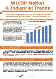
<strong>WLCSP</strong> Market and<br />
Industrial Trends<br />
WEBCAST event – March 2012<br />
Infineon<br />
FhG IZM<br />
STMicro<br />
Broadcom<br />
STEricsson<br />
Hamamatsu<br />
© 2011<br />
Copyrights © Yole Developpement SARL. All rights reserved.
About the authors of this report<br />
Jean-Marc Yannou<br />
– Jean-Marc joined Yole Developpement as technology and market expert in the fields of advanced<br />
packaging and Integrated Passive Devices. He has 15-years of experience in the semiconductor<br />
industry. He worked for Texas Instruments & NXP semiconductors where he was Innovation<br />
Manager for System-in-Package technologies<br />
Contact: yannou@yole.fr<br />
Lionel Cadix<br />
– Lionel joined Yole after the completion of several projects linked to the<br />
characterization and modeling of high density TSV and 3DIC chip stacking in collaboration<br />
with CEA-Leti and STMicroelectronics during his PhD. He is author of several publications and 8<br />
patents in the field of 3D Integration<br />
Contact: cadix@yole.fr<br />
Jerome Baron<br />
– Jerome is leading the MEMS & Advanced Packaging market research at Yole Developpement. He<br />
has been following the 3D packaging market evolution since its early beginnings at device,<br />
equipment and material levels. He was granted a Master of Science degree in Nanotechnologies<br />
from the National Institute of Applied Sciences in Lyon, France<br />
Contact: baron@yole.fr<br />
© 2011 • 2<br />
Copyrights © Yole Développement SA. All rights reserved.
Table of Content of the Report<br />
• Scope of the Report & Definitions …..… 9<br />
- Definitions of wafer scale packaging, wafer level<br />
packaging & wafer level chip scale packaging .………..... 9<br />
- Scope of the report ……..……………………………............ 12<br />
• Executive Summary ….………………….. 17<br />
• <strong>WLCSP</strong> Market Forecasts …................... 43<br />
- Top-down analysis & 2010-2016 unit, wafer and market<br />
forecast …………………………………………………………. 45<br />
- Bottom-up analysis and 2010 production capacity and<br />
market shares ……………………………………………......... 76<br />
- Detailed view of <strong>WLCSP</strong>‟s IC design wins on the market 82<br />
- IC Player capacity for each <strong>WLCSP</strong> application ……….. 89<br />
• <strong>WLCSP</strong> Infrastructure & Supply Chain.. 95<br />
- Supply chain: Fan-in <strong>WLCSP</strong> .…………………...………….. 103<br />
- Supply chain: 3D <strong>WLCSP</strong> …..……………………………….. 111<br />
- Business model examples ………..…………………………. 125<br />
• <strong>WLCSP</strong> Technologies …………………… 140<br />
- RDL, UBM and balling ........................................................ 146<br />
- Test of <strong>WLCSP</strong> ..................................................................... 163<br />
• Cost of <strong>WLCSP</strong> .……….…………… 173<br />
- „Fan-in‟ <strong>WLCSP</strong> cost structure ............................. 174<br />
- 2008-2016 „Fan-in‟ <strong>WLCSP</strong> cost roadmap by<br />
main steps ................................................................ 175<br />
- Cost comparisons of different package<br />
platforms for a 64 I/O device ................................... 179<br />
• <strong>WLCSP</strong> Application Focus ……….. 186<br />
- <strong>WLCSP</strong> ICs in handsets, tablet PCs and MP3 ..... 188<br />
- <strong>WLCSP</strong> ICs for computing ..................................... 214<br />
- <strong>WLCSP</strong> for ICs in medical, automotive & space<br />
applications ……………………………………………<br />
218<br />
- <strong>WLCSP</strong> of CMOS image sensors …………………. 225<br />
- <strong>WLCSP</strong> of MEMS devices ………………………….. 255<br />
• Conclusion & Perspectives ………. 280<br />
• Appendix ……………….................... 283<br />
- Yole Développement company presentation ....... 284<br />
- Company services …………………………………… 285<br />
- Advanced Packaging team analysts ……………… 292<br />
© 2011 • 3<br />
Copyrights © Yole Developpement SARL. All rights reserved.
Scope of the Report<br />
& Definitions<br />
© 2011<br />
Copyrights © Yole Développement SA. All rights reserved.
Scope of Yole‟s Research in Advanced Packaging<br />
PANEL / Wafer-Scale-Packaging Platforms<br />
Wafer-Level<br />
Interface / Encapsulation<br />
Wafer-Level<br />
Electrical Redistribution<br />
Flip-chip & Wafer-Level<br />
Stacking / Integration<br />
<strong>WLCSP</strong><br />
Glass / Silicon<br />
FOWLP Embedded IC 3D IC<br />
WLOptics 2.5D<br />
For MEMS & sensors ‘Fan-in’ ‘Fan-Out’ in PCB / laminate & TSV<br />
interposers<br />
LED & Sensors<br />
3D-<strong>WLCSP</strong><br />
Flip-chip<br />
wafer bumping<br />
on BGA<br />
• Wafer-level-packaging technologies encompass multiple different platform flavors<br />
but leverage similar types of process manufacturing know-how<br />
© 2011 • 5<br />
FOCUS of this<br />
research report update!<br />
Copyrights © Yole Developpement SARL. All rights reserved.
<strong>WLCSP</strong> and 3D <strong>WLCSP</strong> Definition - technology scope of the report<br />
Scope of the report<br />
FOWLP<br />
„Fan-in‟ <strong>WLCSP</strong><br />
+<br />
3D <strong>WLCSP</strong><br />
2.5D<br />
Interposer<br />
3DIC<br />
ST<br />
Elpida<br />
Xilinx<br />
3D<br />
FOWLP<br />
Flip Chip<br />
wafer bumping<br />
• This report does not address all Wafer Level Packaging technologies but only the “Fan-in” type of<br />
<strong>WLCSP</strong>. These include 2 categories:<br />
– Regular <strong>WLCSP</strong> chips: single ICs in <strong>WLCSP</strong> format or CMOS Image Sensors without 3D TSVs or interconnects<br />
– 3D <strong>WLCSP</strong>: <strong>WLCSP</strong> packages with multiple levels / dies / interconnected by means of backside TSVs (Through<br />
Silicon Vias) and wafer-level bonding steps (such as in CMOS image sensors and MEMS devices)<br />
© 2011 • 6<br />
Copyrights © Yole Developpement SARL. All rights reserved.
Difference Between Flip Chip Packages<br />
and Wafer-Level Chip-Scale Packages (<strong>WLCSP</strong>)<br />
With <strong>WLCSP</strong>, the bumped integrated circuits can be directly mounted onto the<br />
Printed Circuit Board of the system by the Original Equipment Maker<br />
Flip Chip packages utilize an intermediate “high density interconnect” (HDI)<br />
printed circuit board<br />
In this report we do not address Flip Chip which is the topic of a separate,<br />
dedicated Yole Market research report<br />
UBM<br />
Underfiller<br />
Bump<br />
Package substrate<br />
© 2011 • 7<br />
Flip Chip<br />
Copyrights © Yole Developpement SARL. All rights reserved.<br />
<strong>WLCSP</strong>
Packaging With Bumping: When is <strong>WLCSP</strong> More Appropriate<br />
With respect to the other WLP technologies?<br />
• <strong>WLCSP</strong> is a wafer-level based package technology with no need for a fan-out area.<br />
It applies to low I/O density ICs with a limited die size (generally lower than<br />
30mm²) and fine ball pitches to the application PCB (equal to or lower than 0.5mm)<br />
Fan-in <strong>WLCSP</strong> Fan-out <strong>WLCSP</strong> Flip Chip<br />
1 2 3 5<br />
This limit will move to<br />
higher ratios as eWLB<br />
production moves from<br />
300mm wafers to large<br />
panels and the cost<br />
of eWLB/fan-out lowers<br />
Package/IC<br />
size ratio*<br />
*package size is determined<br />
by the I/O count and pitch<br />
on the destination PCB<br />
© 2011 • 8<br />
Copyrights © Yole Développement SA. All rights reserved.
Objectives of the Report<br />
• The objectives of this report are<br />
– To describe the Wafer-Level-Packaging market<br />
– To discuss the current technology trends<br />
– To forecast this market‟s future states and trends<br />
• The WLP market is studied from the following angles<br />
– State-of-the-art technology and trends<br />
– End-user applications and drivers<br />
– Materials and equipment<br />
– Market Value<br />
– Industrial supply chain & value chain<br />
– Production cost<br />
© 2011 • 9<br />
Copyrights © Yole Developpement SARL. All rights reserved.
What‟s New Since the “WLP 2009” Report?<br />
• This report is fully focused on the evolution of the <strong>WLCSP</strong> business<br />
– Namely called „Fan-in‟ <strong>WLCSP</strong> and 3D <strong>WLCSP</strong> platforms (please refer to next<br />
slides for more details about definitions)<br />
• What we added/did differently with respect to the 2009 report?<br />
– Deeper analysis of the supply chain for <strong>WLCSP</strong> and 3D <strong>WLCSP</strong><br />
– Top-Down meets Bottom up (whereas the previous report was only based on a<br />
top-down analysis) leading to more exhaustive / detailed market forecasts<br />
– Deeper cost analysis and technologies update<br />
– We now include the value of wafer test in the <strong>WLCSP</strong> market value charts, and<br />
we added a complete section dedicated to test needs and challenges<br />
• Changes in the <strong>WLCSP</strong> ecosystem/infrastructure<br />
– Nokia fall-off in overall demand while more OEM players took to <strong>WLCSP</strong><br />
– More 300mm wafer capacity overall from OSATs, Wafer bumping houses and<br />
IDMs worldwide<br />
– Some new CMOS foundry (TSMC) entrants started to invest additional<br />
capacity in order to provide full Fan-in <strong>WLCSP</strong> turnkey services<br />
© 2011 • 10<br />
Copyrights © Yole Developpement SARL. All rights reserved.
<strong>WLCSP</strong> Market Forecasts<br />
© 2011<br />
Copyrights © Yole Developpement SARL. All rights reserved.
Sales (M$)<br />
Yole‟s Market Forecasting Methodology<br />
• Yole‟s market forecasting methodology is based on the “top-down meets bottom-up” analysis<br />
– 2 complementary analyses are carried out and cross-checked:<br />
• The top-down analysis derives the wafer forecasts from an analysis of the <strong>WLCSP</strong> products, application by application,<br />
taking into account the penetration rate of the technology for each product type, as well as their yields and die sizes<br />
Std. Product<br />
Unit forecasts<br />
Techno<br />
penetration %<br />
<strong>WLCSP</strong> IPD market<br />
In B Munit units<br />
<strong>WLCSP</strong> ASP<br />
$$$<br />
Sources: iSuppli, IC Insights …<br />
Thin film IPD Market Forecast per Application Field (in M$)<br />
1 800<br />
Yole Developpement © June 2009<br />
1 600<br />
1 400<br />
1 200<br />
1 000<br />
800<br />
600<br />
Wafer<br />
Forecasts & 2010<br />
processed wafers<br />
<strong>WLCSP</strong><br />
Die sizes<br />
(mm²)<br />
400<br />
200<br />
Manufacturing 0<br />
Yield<br />
by product<br />
<strong>WLCSP</strong><br />
market<br />
In $M<br />
2008 2009 2010 2011 2012 2013 2014 2015<br />
TOT Thin-film IPD revenues 614 580 631 725 827 1 012 1 276 1 750<br />
• The bottom-up analysis is based on the evaluation of the worldwide production capacity evaluated through interviews of<br />
industry players (foundries, OSATs, equipment and material makers) and company revenue reports. For this report on<br />
<strong>WLCSP</strong>, we used our “wafer bumping for flip chip database”.<br />
Wafer Bumping<br />
capacity<br />
Loading<br />
rate %<br />
2010 Processed<br />
Wafers for<br />
flip chip bumping<br />
© 2011 • 12<br />
• 2010 wafer capacity is therefore estimated using both ways: top-down and bottom-up. The wafer start analysis only stops<br />
when both results are well aligned.<br />
Copyrights © Yole Developpement SARL. All rights reserved.
Sales (M$)<br />
Std. Product<br />
Unit forecasts<br />
Techno<br />
penetration %<br />
<strong>WLCSP</strong> IPD market<br />
In B Munit units<br />
<strong>WLCSP</strong> ASP<br />
$$$<br />
Sources: iSuppli, IC Insights …<br />
Thin film IPD Market Forecast per Application Field (in M$)<br />
1 800<br />
Yole Developpement © June 2009<br />
1 600<br />
1 400<br />
1 200<br />
1 000<br />
800<br />
600<br />
Wafer<br />
Forecasts & 2010<br />
processed wafers<br />
<strong>WLCSP</strong><br />
Die sizes<br />
(mm²)<br />
400<br />
200<br />
Manufacturing 0<br />
Yield<br />
by product<br />
<strong>WLCSP</strong><br />
market<br />
In $M<br />
2008 2009 2010 2011 2012 2013 2014 2015<br />
TOT Thin-film IPD revenues 614 580 631 725 827 1 012 1 276 1 750<br />
TOP-DOWN ANALYSIS<br />
<strong>WLCSP</strong> MARKET VALUE AND FORECASTS<br />
© 2011 • 13<br />
Copyrights © Yole Developpement SARL. All rights reserved.
Market value (M$)<br />
© 2011 • 14<br />
<strong>WLCSP</strong> Market Value Forecast ($M)<br />
<strong>WLCSP</strong> and 3D-<strong>WLCSP</strong><br />
• Total Market value (subcontracted + insourced) of the <strong>WLCSP</strong> wafer and die assembly<br />
services, final test included, based on the price of the subcontracted service by OSATs<br />
• The Fan-in <strong>WLCSP</strong> market value<br />
totaled close to $1.4B in 2010, of which<br />
– $1091M for <strong>WLCSP</strong> of ICs<br />
– and $300M of CMOS image<br />
sensors and MEMS<br />
• The 3D-<strong>WLCSP</strong> market is expected to<br />
grow at a 2010-2016 CAGR of 25% fostered<br />
by both the fast growth rate of MEMS and CIS<br />
and by the acceleration of the penetration<br />
of WLP packages for these devices.<br />
• The <strong>WLCSP</strong> market value for<br />
integrated circuits is expected<br />
to grow at a 2010-2016 CAGR of 7%.<br />
It is significantly lower than the 16.5% growth<br />
rate of this market as expressed in<br />
300mm equivalent wafers over the same<br />
period of time due to<br />
– Declining margins<br />
– Fast adoption of lower cost<br />
<strong>WLCSP</strong> on 300mm wafers (in terms<br />
of cost per die)<br />
Copyrights © Yole Developpement SARL. All rights reserved.<br />
3 000<br />
2 500<br />
2 000<br />
1 500<br />
1 000<br />
500<br />
0<br />
<strong>WLCSP</strong> Market Value ($M)<br />
Yole Developpement © September 2011<br />
2010 2011 2012 2013 2014 2015 2016<br />
3D<strong>WLCSP</strong> market (M$) 267,9 384,1 511,4 618,9 716,3 856,4 1001,3<br />
<strong>WLCSP</strong> market (M$) 1120,0 1277,8 1389,9 1480,1 1567,2 1632,8 1669,2
<strong>WLCSP</strong> Adoption Drivers<br />
• Drivers for <strong>WLCSP</strong><br />
– Footprint reduction die size = package size<br />
– Electrical performance bumps have a lower inductance than wire-bonds<br />
– Legacy die converted to <strong>WLCSP</strong> through use of RDL (lower price and no need for<br />
silicon redesign)<br />
– Thin package profile (Z < 1.0mm)<br />
– Cost is competitive with other package types<br />
• Developments and evolutions<br />
– Thinner package height ( improve routing<br />
• 2 primary Board Level Reliability tests are important for <strong>WLCSP</strong> performance: Drop<br />
test (DT) and Temperature Cycling Test (TCT)<br />
© 2011 • 15<br />
Copyrights © Yole Developpement SARL. All rights reserved.
Examples of <strong>WLCSP</strong> Penetration in Real Products<br />
Yole Developpement<br />
© September 2011<br />
Relative package uses in end devices<br />
(in % of units by package type)<br />
100%<br />
90%<br />
80%<br />
70%<br />
60%<br />
50%<br />
40%<br />
30%<br />
20%<br />
10%<br />
0%<br />
Motorola<br />
Atrix 4G<br />
Apple<br />
iPaD2<br />
Samsung<br />
Galaxy tab<br />
Gt P-1000<br />
Nokia N8-<br />
00<br />
Blackberry<br />
Bold 9700<br />
Google<br />
(Samsung)<br />
Nexus S GT<br />
Apple<br />
iPhone 3GS<br />
iPoD touch<br />
2nd<br />
generation<br />
8GB<br />
Apple Max<br />
Mini A1347<br />
QFP 0% 0% 0% 0% 0% 0% 0% 0% 0% 5%<br />
SO/SOT/TSSOP 3% 3% 10% 0% 0% 26% 12% 0% 41% 49%<br />
LGA 3% 5% 5% 2% 0% 4% 2% 0% 0% 0%<br />
BGA 27% 30% 19% 15% 28% 13% 21% 20% 9% 5%<br />
DFN/QFN 37% 33% 45% 6% 13% 39% 28% 15% 48% 41%<br />
<strong>WLCSP</strong> 30% 30% 21% 77% 60% 17% 37% 65% 2% 0%<br />
Lenovo<br />
IdeaPad<br />
S10<br />
© 2011 • 16<br />
Copyrights © Yole Developpement SARL. All rights reserved.<br />
tablets smartphones MP3/PMP PC
Device count (Mu)<br />
2010-2016 <strong>WLCSP</strong> Unit Forecast - by end equipment type<br />
50 000<br />
45 000<br />
<strong>WLCSP</strong> forecast<br />
by end equipment type (in M unit shipments)<br />
Yole Developpement © September 2011<br />
40 000<br />
35 000<br />
30 000<br />
25 000<br />
20 000<br />
15 000<br />
10 000<br />
5 000<br />
0<br />
2010 2011 2012 2013 2014 2015 2016<br />
others (medical, automotive...) 700 770 847 932 1044 1169 1309<br />
notebooks 36 43 51 61 73 87 101<br />
set top box<br />
2 3 4 5 5 5 5<br />
PMP/MP3 1 675 1 602 1 496 1 402 1 316 1 250 1 201<br />
tablets 241 784 1 315 1 920 2 671 3 487 4 200<br />
smartphones 5 302 7 523 9 800 12 075 14 481 17 016 19 343<br />
feature phones 8 501 9 779 11 025 12 463 13 804 15 258 16 519<br />
voice phone 3 430 3 178 3 036 2 899 2 803 2 657 2 522<br />
CAGR (%)<br />
11.0<br />
18.7<br />
22.2<br />
-5.4<br />
61.0<br />
24.0<br />
11.7<br />
-5.0<br />
© 2011 • 17<br />
total 19,887 23,682 27,575 31,756 36,197 40,929 45,201 14.66<br />
Copyrights © Yole Developpement SARL. All rights reserved.
<strong>WLCSP</strong> Penetration Status in Mobile Platforms<br />
CPU<br />
In grey: parts which can not be<br />
found in „Fan-in‟ <strong>WLCSP</strong> form<br />
Drivers<br />
In orange: these devices are increasingly<br />
packaged in „Fan-in‟ <strong>WLCSP</strong>!<br />
Discrete passives<br />
• This is by far the largest „Fan-in‟ <strong>WLCSP</strong> end application<br />
• <strong>WLCSP</strong> ICs started in 2000 in handsets,<br />
with small ESD/EMI<br />
protection/interface conditioning<br />
devices Integrated Passive<br />
Devices (IPD) at first, and<br />
then with larger<br />
ICs.<br />
• The drivers<br />
are Size<br />
(footprint<br />
first, then<br />
thinness &<br />
weight) and<br />
Cost<br />
© 2011 • 18<br />
Copyrights © Yole Developpement SARL. All rights reserved.
<strong>WLCSP</strong> Device Categories<br />
<strong>WLCSP</strong> device categories<br />
Analog &<br />
mixed signal<br />
Wireless<br />
Connectivity<br />
Opto<br />
MEMS & sensors<br />
ASIC IC<br />
MEMS<br />
IPD (ESD/EMI<br />
protection, RF filtering)<br />
Power Amplifiers<br />
BAW & SAW filters<br />
IC drivers (LED,<br />
battery, display…)<br />
Local Power<br />
(DC-DC converters,<br />
MOSFET, oscillators)<br />
PMU<br />
Audio & Video<br />
(Codec, amplifiers…)<br />
Bluetooth +<br />
FM + WLAN<br />
combos<br />
(+ combos)<br />
WLAN single<br />
chip<br />
GPS, A-GPS<br />
single chip<br />
CMOS image<br />
sensors<br />
AL sensor<br />
photonic<br />
Misc Logic<br />
and Memory<br />
Logic gates<br />
EEPROMs<br />
µcontrollers<br />
Accelerometers<br />
Gyroscopes<br />
RF-MEMS (switches,<br />
resonators…)<br />
Si Microphones<br />
Pressure sensors<br />
Optical MEMS<br />
micro-mirrors (DLP,<br />
pico-projectors, datacom)<br />
µ-probes<br />
µ-fluidic, µ-fuel cells<br />
© 2011 • 19<br />
Copyrights © Yole Developpement SARL. All rights reserved.
Wafer Bumping<br />
capacity<br />
Loading<br />
rate %<br />
2010 Processed<br />
Wafers for<br />
flip chip bumping<br />
BOTTOM-UP ANALYSIS<br />
2010 <strong>WLCSP</strong> INDUSTRY STATUS AND<br />
WAFER PROCESSING CAPACITY<br />
© 2011 • 20<br />
Copyrights © Yole Developpement SARL. All rights reserved.
2010 <strong>WLCSP</strong> + 3D <strong>WLCSP</strong> Regional Capacities<br />
Korea<br />
192,000 wafers<br />
8%<br />
China<br />
199,800 wafers<br />
8%<br />
2010 <strong>WLCSP</strong> + 3D <strong>WLCSP</strong> geographic installed capacities<br />
(300mm eq. wafers)<br />
Singapore<br />
144,000 wafers<br />
6%<br />
Philippines<br />
127,200 wafers<br />
5%<br />
Malaysia<br />
46,800 wafers<br />
2%<br />
Thailand<br />
36,000<br />
2%<br />
Canada<br />
19,800<br />
wafers<br />
1%<br />
Morocco<br />
5,280 wafers<br />
0%<br />
Taiwan<br />
947,400 wafers<br />
39%<br />
TOT ~ 2.4 Million<br />
wafers (300mm eq.)<br />
USA<br />
189,600 wafers<br />
8%<br />
Europe<br />
190,800 wafers<br />
8%<br />
Japan<br />
308,400 wafers<br />
13%<br />
Yole Developpement ©<br />
September 2011<br />
© 2011 • 21<br />
Copyrights © Yole Developpement SARL. All rights reserved.
<strong>WLCSP</strong> Infrastructure<br />
& Supply Chain<br />
© 2011<br />
Copyrights © Yole Developpement SARL. All rights reserved.
Supply Chain for <strong>WLCSP</strong> Manufacturing<br />
<strong>WLCSP</strong> operations<br />
PVD / Plating equipment<br />
Passivation resist suppliers<br />
IC design<br />
Si CMOS<br />
manufacturing<br />
RDL / Passivation<br />
Balling<br />
Wafer test Back-end: OEM /<br />
dicing, marking, T&R EMS<br />
Fully integrated IDMs<br />
Vertical integration?<br />
Fabless<br />
CMOS<br />
foundries<br />
Wafer bumping house<br />
Test house<br />
BE service<br />
Wafer Packaging House<br />
OSAT<br />
© 2011 • 23<br />
Copyrights © Yole Developpement SARL. All rights reserved.
<strong>WLCSP</strong> Design Wins for Small Logic, Memory and RF Connectivity<br />
IC design<br />
companies<br />
logic gates /<br />
bus buffers /<br />
level<br />
translators<br />
EEPROM / serial<br />
Flash memories<br />
SRAM<br />
memories<br />
Microcontroller<br />
Bluetooth + FM<br />
chip<br />
GPS<br />
chip<br />
WLAN (single<br />
chip)<br />
Combos (mix of<br />
WLAN / BT / FM<br />
/ GPS)<br />
Atmel (US)<br />
X<br />
Broadcom (US) X X X<br />
CSR (US) X X X<br />
Cypress Semi (US)<br />
X<br />
Infineon (GE)<br />
X<br />
Macronix (TW)<br />
X<br />
Marvell (US)<br />
X<br />
Maxim IC (US)<br />
Microchip (US)<br />
X<br />
X<br />
Qualcomm / Atheros (US)<br />
X<br />
SST / Green Liant (US)<br />
X<br />
STEricsson (FR)<br />
X<br />
STMicroelectronics (FR) X X<br />
Texas Instruments (US) X X X X X<br />
© 2011 • 24<br />
Copyrights © Yole Developpement SARL. All rights reserved.
Texas Instrument‟s <strong>WLCSP</strong> wafer shipment<br />
Breakdown by application (12’’ eq wspy)<br />
2010 Texas Instruments' <strong>WLCSP</strong> wafer shipments<br />
Breakdown by application (12'' eq wspy)<br />
Yole Developpement ©<br />
September 2011<br />
Combos (mix of WLAN / BT / FM<br />
/ GPS)<br />
50 000<br />
20%<br />
IPD (ESD / EMI)<br />
10 000<br />
4%<br />
DC/DC converter, LDO<br />
30 000<br />
12%<br />
Amplifier, generator, analog<br />
switches IC drivers, RF power<br />
detectors<br />
15 000<br />
6%<br />
WLAN (single chip)<br />
25 000<br />
10%<br />
Touch screen controller<br />
3 600<br />
1%<br />
GPS chip<br />
20 750<br />
8%<br />
microcontroller<br />
4 000<br />
2%<br />
logic gates / bus buffers / level<br />
LED drivers<br />
translators<br />
3 300<br />
40 000<br />
1%<br />
16%<br />
battery charger<br />
25 000<br />
10%<br />
Audio / Video codec<br />
15 000<br />
6%<br />
Audio power amplfier/ video<br />
driver (amplifier, noise canceler,<br />
TV tuner etc…)<br />
5000<br />
2%<br />
• Texas Instruments (US) can be considered as #1 company in the <strong>WLCSP</strong> area since the company<br />
has a diversified product portfolio of analog IC design wins in <strong>WLCSP</strong> plus important internal<br />
capabilities for Fan-in <strong>WLCSP</strong> manufacturing (in its Clark facility in Philippines)<br />
© 2011 • 25<br />
Copyrights © Yole Developpement SARL. All rights reserved.
<strong>WLCSP</strong> Technologies<br />
© 2011<br />
Copyrights © Yole Developpement SARL. All rights reserved.
<strong>WLCSP</strong> Technology & Industrial Roadmap<br />
Demonstrated On the market!<br />
Silicon node<br />
65nm<br />
45nm<br />
32 / 22nm<br />
PCB pitch<br />
0.4 - 0.5mm<br />
0.25 - 0.3mm<br />
Minimum Line/space<br />
15/15um<br />
12/12um<br />
10/10um<br />
<strong>WLCSP</strong><br />
techno<br />
Wafer thickness<br />
> 30- 40 mm 2<br />
Max die size 0.6 - 27mm 2 250 – 350um<br />
200 – 300um<br />
150 – 250um<br />
New equipment<br />
DRIE<br />
Grinding & CMP<br />
Laser dicing<br />
inspection<br />
Passivation material<br />
BCB, PI<br />
PI, PBO, Al-X, etc…<br />
Package integration<br />
TSV (3D WLP)<br />
Fan-in only<br />
Fan-out / Embedding<br />
IPD<br />
<strong>WLCSP</strong><br />
infrastructure<br />
12 inch<br />
wafers<br />
Solar<br />
infrastructure?<br />
< 2007<br />
2008<br />
2009<br />
2010 2011 2012 2013 2014 2015<br />
© 2009 • 27<br />
Copyrights © Yole Développement SARL. All rights reserved.
<strong>WLCSP</strong> Extending to Higher I/O Levels in PMU Applications<br />
• The largest <strong>WLCSP</strong> IC on the market: Fujitsu MB38C311A<br />
– 309 <strong>WLCSP</strong> balls: world record highest <strong>WLCSP</strong> pin count<br />
– 50mm²<br />
– 0.4mm pitch<br />
– Designed and manufactured by Casio Micronics (now TeraMikros)<br />
– Balls on copper posts: eWLP technology<br />
– PMU + Audio interface functions combined<br />
– Found in Sharp SH-01A phone<br />
Pictures are courtesy of ‘System Plus Consulting’<br />
© 2011 • 28<br />
Copyrights © Yole Developpement SARL. All rights reserved.
<strong>WLCSP</strong> for Audio Amplifier<br />
• By using <strong>WLCSP</strong>, the audio control chip and amplification IC of the iPod Shuffle<br />
could be squeezed in the headphones, making it compulsory to use the Apple<br />
headphones or some specific headphones under Apple license (the shuffle device<br />
has no audio circuitry) The IC (1.35 mm x 0.85) is made by Texas Instruments<br />
© 2011 • 29<br />
WLP of Class D audio amplifiers from TI<br />
Copyrights © Yole Developpement SARL. All rights reserved.
VTI – 3D Axis Accelerometer<br />
a 3D-<strong>WLCSP</strong> example<br />
• The <strong>WLCSP</strong> package of the CMR3000 integrates two dies (ASIC + MEMS). The<br />
ASIC die is flip-chipped on the MEMS die (the gap between the 2 dies is<br />
underfilled)<br />
• The ASIC die is manufactured using a CMOS technology with a 0.4μm process.<br />
• The MEMS die is manufactured using three bonded wafers (c-SOI sensor + Cap)<br />
processed with bulk micromachining technologies.<br />
Package type: 10-pin WLP<br />
• Dimensions: 4.10mm x 3.10mm x 0.83mm<br />
• Pin pitch: 0.50mm<br />
Courtesy of Chipworks<br />
© 2011 • 30<br />
Copyrights © Yole Developpement SARL. All rights reserved.
Conclusions & Perspectives<br />
© 2011<br />
Copyrights © Yole Developpement SARL. All rights reserved.
Conclusions<br />
• The number of devices packaged with „Fan-in‟ <strong>WLCSP</strong> will exceed 25 Billion units in 2012,<br />
exceeding more than 2 million 300mm equivalent wafers<br />
• We estimate that the „Fan-in‟ <strong>WLCSP</strong> industry value to be over 1.9 billion dollars in 2012.<br />
This includes wafer level services (including test) and die level services, as well as the<br />
service margin<br />
• This market value is expected to keep on growing at a 2010-2016 CAGR of 12% despite<br />
decreasing prices. However it does not grow equally across all device types<br />
• The use of „Fan-in‟ <strong>WLCSP</strong> for a given application tends to be more and more standardized:<br />
it is now clear, for example, that the penetration rate of „Fan-in‟ <strong>WLCSP</strong> for connectivity<br />
devices in handsets is close to 100%, while some players still proposed QFN or BGA<br />
solutions a couple of years ago for this same application<br />
• The maximum die size increased recently, and it is now common place to find 36mm² „Fanin‟<br />
<strong>WLCSP</strong> devices in smartphones and tablets. The world record is 50mm² with 309 balls.<br />
Any „Fan-in‟ <strong>WLCSP</strong> device larger than 4mm in side needs to be underfilled on the PCB<br />
• „Fan-in‟ <strong>WLCSP</strong> is a maturing technology and market. It still grows faster than the average<br />
semiconductor packaging market mainly thanks to the fast growth rates of smartphones and<br />
tablet PCs in which <strong>WLCSP</strong> considerably helps save space and costs.<br />
© 2011 • 32<br />
Copyrights © Yole Developpement SARL. All rights reserved.
© 2009<br />
Osram<br />
IR<br />
Copyrights © Yole Dévelo pement SARL. A l rights reserved.<br />
Yole activities in Advanced Packaging<br />
Media business<br />
News feed / Magazines / Webcasts<br />
Market Research<br />
Reports<br />
Market research,<br />
Technology & Strategy<br />
Consulting services<br />
www.yole.fr<br />
HB-LED Packaging<br />
Technology & Market Trends<br />
© 2011 • 33<br />
Copyrights © Yole Developpement SARL. All rights reserved.
Osram<br />
IR<br />
Copyrights © Yole Développement SARL. All rights reserved.<br />
EVG<br />
SUSS<br />
DuPont<br />
NEC-Schott<br />
STS<br />
Brewer Science<br />
Copyrights © Yole Développement SARL. All rights reserved.<br />
N<br />
o<br />
k<br />
i<br />
a<br />
F<br />
r<br />
e<br />
e<br />
s<br />
c<br />
a<br />
l<br />
e<br />
S<br />
i<br />
l<br />
e<br />
x<br />
D<br />
u<br />
P<br />
o<br />
n<br />
t<br />
Copyrights © Yole Développement SA. All rights reserved.<br />
I<br />
M<br />
E<br />
C<br />
N<br />
o<br />
k<br />
i<br />
a<br />
F<br />
r<br />
e<br />
e<br />
s<br />
c<br />
a<br />
l<br />
e<br />
S<br />
i<br />
l<br />
e<br />
x<br />
D<br />
u<br />
P<br />
o<br />
n<br />
t<br />
I<br />
M<br />
E<br />
C<br />
Our latest packaging market reports<br />
HB-LED Packaging<br />
Technology & Market Trends<br />
Equipment Advanced Packaging<br />
& Materials<br />
for 3DIC & Wafer-Level-Packaging<br />
Equipment & Materials<br />
Via First / Via Last?<br />
3D integration Scenarios<br />
3D IC & TSV<br />
2010 Market Analysis<br />
© 2009<br />
© 2010<br />
FO WLP &<br />
Embedded die<br />
WL CSP<br />
2011 Report update<br />
3D Glass & Silicon<br />
interposers - 2010 Report<br />
IPD - Thin-film<br />
Integrated Passive Devices<br />
N<br />
o<br />
k<br />
i<br />
a<br />
TSV +<br />
Cost Analysis Tool for<br />
your 3D IC manufacturing<br />
Wafer Packaging Fabs<br />
DATABASE<br />
MEMS Packaging<br />
Market & Technology Trends<br />
Flip-chip<br />
2011 Report<br />
TSV Scenario Cost structure breakdown<br />
$27<br />
7% $23<br />
6%<br />
$168<br />
$109<br />
41%<br />
26%<br />
$8<br />
$31<br />
$9 $37 2%<br />
7%<br />
2% 9%<br />
Via / Etching Drilling<br />
Via Isolation<br />
Via filling<br />
Temporary bonding<br />
Thinning<br />
Stress release<br />
BEOL (Pads)<br />
Bonding<br />
© 2010<br />
6 & 6 mm<br />
6 & 6 mm<br />
1995<br />
~125 sq mm ~100 sq mm ~25 sq mm<br />
1996-2002<br />
1999 - today 2006<br />
1995<br />
~125 sq mm ~100 sq mm ~25 sq mm<br />
1996-2002<br />
1999 - today 2006<br />
Sidebraze DIP<br />
Plastic PDIP<br />
SMT SOIC<br />
& Die Down<br />
Stacked Die<br />
QFN<br />
Sidebraze DIP<br />
Plastic PDIP<br />
SMT SOIC<br />
& Die Down<br />
Stacked Die<br />
QFN<br />
© 2011 • 34<br />
Copyrights © Yole Developpement SARL. All rights reserved.


