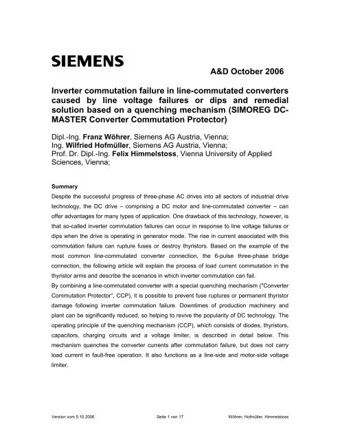
A&D October 2006 Inverter commutation failure in line ... - Siemens
A&D October 2006 Inverter commutation failure in line ... - Siemens
A&D October 2006 Inverter commutation failure in line ... - Siemens
Create successful ePaper yourself
Turn your PDF publications into a flip-book with our unique Google optimized e-Paper software.
A&D <strong>October</strong> <strong>2006</strong><br />
<strong>Inverter</strong> <strong>commutation</strong> <strong>failure</strong> <strong>in</strong> l<strong>in</strong>e-commutated converters<br />
caused by l<strong>in</strong>e voltage <strong>failure</strong>s or dips and remedial<br />
solution based on a quench<strong>in</strong>g mechanism (SIMOREG DC-<br />
MASTER Converter Commutation Protector)<br />
Dipl.-Ing. Franz Wöhrer, <strong>Siemens</strong> AG Austria, Vienna;<br />
Ing. Wilfried Hofmüller, <strong>Siemens</strong> AG Austria, Vienna;<br />
Prof. Dr. Dipl.-Ing. Felix Himmelstoss, Vienna University of Applied<br />
Sciences, Vienna;<br />
Summary<br />
Despite the successful progress of three-phase AC drives <strong>in</strong>to all sectors of <strong>in</strong>dustrial drive<br />
technology, the DC drive – compris<strong>in</strong>g a DC motor and l<strong>in</strong>e-commutated converter – can<br />
offer advantages for many types of application. One drawback of this technology, however, is<br />
that so-called <strong>in</strong>verter <strong>commutation</strong> <strong>failure</strong>s can occur <strong>in</strong> response to l<strong>in</strong>e voltage <strong>failure</strong>s or<br />
dips when the drive is operat<strong>in</strong>g <strong>in</strong> generator mode. The rise <strong>in</strong> current associated with this<br />
<strong>commutation</strong> <strong>failure</strong> can rupture fuses or destroy thyristors. Based on the example of the<br />
most common l<strong>in</strong>e-commutated converter connection, the 6-pulse three-phase bridge<br />
connection, the follow<strong>in</strong>g article will expla<strong>in</strong> the process of load current <strong>commutation</strong> <strong>in</strong> the<br />
thyristor arms and describe the scenarios <strong>in</strong> which <strong>in</strong>verter <strong>commutation</strong> can fail.<br />
By comb<strong>in</strong><strong>in</strong>g a l<strong>in</strong>e-commutated converter with a special quench<strong>in</strong>g mechanism ("Converter<br />
Commutation Protector“, CCP), it is possible to prevent fuse ruptures or permanent thyristor<br />
damage follow<strong>in</strong>g <strong>in</strong>verter <strong>commutation</strong> <strong>failure</strong>. Downtimes of production mach<strong>in</strong>ery and<br />
plant can be significantly reduced, so help<strong>in</strong>g to revive the popularity of DC technology. The<br />
operat<strong>in</strong>g pr<strong>in</strong>ciple of the quench<strong>in</strong>g mechanism (CCP), which consists of diodes, thyristors,<br />
capacitors, charg<strong>in</strong>g circuits and a voltage limiter, is described <strong>in</strong> detail below. This<br />
mechanism quenches the converter currents after <strong>commutation</strong> <strong>failure</strong>, but does not carry<br />
load current <strong>in</strong> fault-free operation. It also functions as a l<strong>in</strong>e-side and motor-side voltage<br />
limiter.<br />
Version vom 5.10.<strong>2006</strong> Seite 1 von 17 Wöhrer, Hofmüller, Himmelstoss
1. Introduction<br />
Despite the successful progress of three-phase AC drives, compris<strong>in</strong>g a frequency converter<br />
and three-phase motor, <strong>in</strong>to all sectors of <strong>in</strong>dustrial drive technology, the tried and tested DC<br />
drive, consist<strong>in</strong>g of a DC motor and l<strong>in</strong>e-commutated converter, still plays an important role <strong>in</strong><br />
many applications and is still the drive of choice for many new <strong>in</strong>stallations.<br />
To make the right decision as to whether a DC or AC drive system is the better option for a<br />
particular application, it is necessary to evaluate the whole system, i.e. the motor, the supply<br />
power section and any other necessary additional electrical components such as l<strong>in</strong>e filters<br />
or commutat<strong>in</strong>g reactors.<br />
A decision <strong>in</strong> favor of DC drive technology is often <strong>in</strong>fluenced by the significantly lower power<br />
loss of the power electronic components, the space-sav<strong>in</strong>g design and the lower cost of the<br />
overall drive system.<br />
In addition to the <strong>in</strong>creased ma<strong>in</strong>tenance requirements for DC motors as compared to AC<br />
motors, there is one other disadvantage which weighs aga<strong>in</strong>st DC drive technology. This is<br />
the problem of so-called "<strong>in</strong>verter <strong>commutation</strong> <strong>failure</strong>", a fault which can occur under certa<strong>in</strong><br />
operat<strong>in</strong>g conditions and which causes fuses to blow and, <strong>in</strong> the worst-case scenario,<br />
permanent thyristor damage.<br />
2. The 6-pulse three-phase bridge connection<br />
The most common form of l<strong>in</strong>e-commutated converter connection, i.e. the controlled 6-pulse<br />
three-phase bridge connection (B6C) as shown <strong>in</strong> Figure 1 is exam<strong>in</strong>ed below. Separately<br />
excited DC mach<strong>in</strong>es are employed for most <strong>in</strong>dustrial applications which use DC drives.<br />
Figure 1 shows the armature circuit of the DC mach<strong>in</strong>e as an equivalent circuit diagram<br />
compris<strong>in</strong>g armature circuit <strong>in</strong>ductance L a , armature circuit resistance R a and the <strong>in</strong>duced<br />
source voltage U q .<br />
u 31<br />
u 12<br />
u 23<br />
V1 V3 V5<br />
L K<br />
L K<br />
I d<br />
u d α<br />
R a<br />
L a<br />
U q<br />
Controlled 6-pulse threephase<br />
bridge connection<br />
(B6C) for supply<strong>in</strong>g the<br />
armature circuit of a<br />
separately excited DC<br />
V4 V6 V2<br />
mach<strong>in</strong>e<br />
a<br />
Version vom 5.10.<strong>2006</strong> Seite 2 von 17 Wöhrer, Hofmüller, Himmelstoss
L K<br />
V1<br />
I d<br />
R a<br />
Armature current I d passes<br />
through V1 and V2.<br />
u 13<br />
u 13 → u d α<br />
L a<br />
L K<br />
V2<br />
U q<br />
b<br />
u 13<br />
u 12<br />
u 23<br />
V1 V3<br />
L K<br />
i K21<br />
L K<br />
i v1<br />
u 21 L K<br />
i v3<br />
I d<br />
u13 + u23<br />
→ udα<br />
2<br />
R a<br />
L a<br />
The <strong>commutation</strong> period<br />
commences when V3 is fired.<br />
The "commutat<strong>in</strong>g" l<strong>in</strong>e<br />
voltage u 21 causes shortcircuit<br />
current i k21 to develop U q .<br />
V2<br />
c<br />
V3<br />
I d<br />
R a<br />
After successful<br />
<strong>commutation</strong>, armature<br />
u 23<br />
L K<br />
L K<br />
u 23 →u<br />
d α<br />
L a<br />
current I d flows through V3<br />
and V2.<br />
V2<br />
U q<br />
d<br />
Figure 1 a Controlled 6-pulse three-phase bridge connection (B6C), b to d show the 3<br />
phases of <strong>commutation</strong> illustrated by the example of <strong>commutation</strong> sequence of<br />
thyristor V1 to thyristor V3<br />
The thyristor bridge, consist<strong>in</strong>g of thyristors V1 to V6, is supplied by an idealized 3-phase<br />
voltage system (l<strong>in</strong>e-to-l<strong>in</strong>e s<strong>in</strong>usoidal voltages u 12 , u 23 , u 31 ). The <strong>in</strong>ductance L k <strong>in</strong>cludes all<br />
the <strong>in</strong>ductance of the supply system plus the effective <strong>in</strong>ductance of l<strong>in</strong>e-side transformers<br />
and commutat<strong>in</strong>g reactors. The operat<strong>in</strong>g pr<strong>in</strong>ciple of this converter type is based on the<br />
well-known "l<strong>in</strong>e <strong>commutation</strong>" method, i.e. the thyristors must be fired <strong>in</strong> such a sequence<br />
that the load current I d flow<strong>in</strong>g through the DC mach<strong>in</strong>e is always switched from one l<strong>in</strong>e<br />
phase to the next (u 12 → u 13 → u 23 → u 21 → u 31 → u 32 ). The thyristors are numbered (1 to 6)<br />
<strong>in</strong> the same sequence <strong>in</strong> which they are fired when a 3-phase voltage supply with clockwise<br />
phase sequence is applied (i.e. u 23 lags 120 degrees and u 31 lags 240 degrees beh<strong>in</strong>d the<br />
l<strong>in</strong>e-to-l<strong>in</strong>e voltage u 12 ). In steady-state operation, a "new" thyristor is fired at every 60 degree<br />
<strong>in</strong>terval. To allow conduction with a discont<strong>in</strong>uous load current, the previously conduct<strong>in</strong>g<br />
Version vom 5.10.<strong>2006</strong> Seite 3 von 17 Wöhrer, Hofmüller, Himmelstoss
thyristor must be fired simultaneously, a process which has given rise to the term "double<br />
pulses". Each thyristor conducts the load current for 2 successive fir<strong>in</strong>g cycles (twice with<strong>in</strong> a<br />
maximum of 60 degrees <strong>in</strong> steady state).<br />
The average value of the rectified output voltage u dα can be adjusted by the so-called delay<br />
or gat<strong>in</strong>g angle α. The delay angle α is measured from the so-called "natural <strong>commutation</strong><br />
<strong>in</strong>stant“ N. This is the po<strong>in</strong>t at which current <strong>commutation</strong> would commence <strong>in</strong> a new l<strong>in</strong>e<br />
phase <strong>in</strong> a diode bridge (<strong>in</strong>tersection between u 12 and u 13 , u 13 and u 23 , u 23 and u 21 , u 21 and<br />
u 31 , u 31 and u 32 , u 32 and u 12 ).<br />
One segment at a time (with <strong>in</strong>terval that can be varied by delay angle α) from one of the<br />
l<strong>in</strong>e-to-l<strong>in</strong>e supply voltages (u 13 , u 23 , u 21 , u 31 , u 32 , u 12 ) is "switched through" cont<strong>in</strong>uously to<br />
the DC mach<strong>in</strong>e via a pair of thyristors (V1+V2, V2+V3, V3+V4, V4+V5, V5+V6, V6+V1).<br />
Due to the <strong>in</strong>ductance L k <strong>in</strong> the circuit, however, the load current I d cannot transfer<br />
<strong>in</strong>stantaneously from the outgo<strong>in</strong>g ("turn<strong>in</strong>g off") thyristor arm to the <strong>in</strong>com<strong>in</strong>g ("turn<strong>in</strong>g on")<br />
thyristor arm. With a cont<strong>in</strong>uous load current I d , the "<strong>commutation</strong> period" or "overlap"<br />
commences <strong>in</strong> each case when the "new" (<strong>in</strong>com<strong>in</strong>g) thyristor is fired, while the load current<br />
I d from one term<strong>in</strong>al of the DC mach<strong>in</strong>e is split between two l<strong>in</strong>e phases via the outgo<strong>in</strong>g and<br />
<strong>in</strong>com<strong>in</strong>g thyristors. The other term<strong>in</strong>al of the DC mach<strong>in</strong>e is connected to the rema<strong>in</strong><strong>in</strong>g<br />
supply connection via the thyristor fired <strong>in</strong> the previous cycle, which is now <strong>in</strong> the second<br />
conduction phase and conduct<strong>in</strong>g the full load current I d .<br />
While the 6-pulse three-phase bridge connection can supply only a positive load current I d , it<br />
is capable of generat<strong>in</strong>g positive or negative average values of the rectified output voltage<br />
u dα through variation of delay angle α. Depend<strong>in</strong>g on whether the DC mach<strong>in</strong>e is operat<strong>in</strong>g<br />
as a motor or generator, the converter bridge is said to be operat<strong>in</strong>g <strong>in</strong> "rectifier mode" or<br />
"<strong>in</strong>verter mode". A s<strong>in</strong>gle three-phase bridge connection is therefore suitable for a drive with<br />
only positive torque <strong>in</strong> different directions of rotation. A typical application for this type of<br />
operation <strong>in</strong> the 1st and 4th speed/torque quadrant would be the hoist<strong>in</strong>g or lower<strong>in</strong>g of a<br />
hoist load. If the DC mach<strong>in</strong>e is also required to operate with negative torques, then a double<br />
converter (also referred to as "reversible converter") must be used. The most common<br />
design of reversible converter is based on a circulat<strong>in</strong>g-current-free anti-parallel connection<br />
of two three-phase bridge connections.<br />
Version vom 5.10.<strong>2006</strong> Seite 4 von 17 Wöhrer, Hofmüller, Himmelstoss
3. Commutation of current <strong>in</strong> thyristor arms<br />
To expla<strong>in</strong> the process of <strong>in</strong>verter <strong>commutation</strong> <strong>failure</strong>, <strong>commutation</strong> of the load current from<br />
V1 to V3 as illustrated <strong>in</strong> Figure 1 b to d is exam<strong>in</strong>ed <strong>in</strong> more detail <strong>in</strong> the follow<strong>in</strong>g example.<br />
The voltage and current waveforms associated with this type of <strong>commutation</strong> <strong>in</strong> regenerative<br />
feedback mode are shown <strong>in</strong> Figure 2.<br />
In the <strong>in</strong>itial state (as shown <strong>in</strong> Figure 1 b), the full load current I d flows across thyristors V1<br />
and V2 and, as a result, the l<strong>in</strong>e voltage u 13 is "switched through" to the output.<br />
At <strong>in</strong>stant ωt D as shown <strong>in</strong> Figure 2, i.e. delayed by angle α <strong>in</strong> relation to the natural<br />
<strong>commutation</strong> <strong>in</strong>stant N, the "new" (<strong>in</strong>com<strong>in</strong>g) thyristor V3 is fired for the purpose of switch<strong>in</strong>g<br />
through the l<strong>in</strong>e-to-l<strong>in</strong>e supply voltage u 23 <strong>in</strong> the correct phase sequence to the output<br />
(thyristor V2 is fired simultaneously). Due to the <strong>in</strong>ductance L k <strong>in</strong> the circuit, the current<br />
cannot transfer <strong>in</strong>stantaneously from V1 to V3. The period of "<strong>commutation</strong>" or "overlap"<br />
commences while the load current I d is split between V1 (i V1 ) and V3 (i V3 ) (<strong>in</strong>terval between<br />
ωt D and ωt E as shown <strong>in</strong> Figure 2).<br />
If the <strong>in</strong>ductance <strong>in</strong> the load circuit (armature <strong>in</strong>ductance L a of DC mach<strong>in</strong>e <strong>in</strong>clud<strong>in</strong>g an<br />
armature current smooth<strong>in</strong>g reactor if used) is very much higher than the effective<br />
<strong>commutation</strong> <strong>in</strong>ductance L k , then the load current I d can be regarded as an approximately<br />
constant quantity over the <strong>commutation</strong> period (the armature circuit <strong>in</strong>ductance L a acts like a<br />
power source).<br />
Figure 1 c shows that the l<strong>in</strong>e-to-l<strong>in</strong>e supply voltage u 21 (i.e. the difference between the l<strong>in</strong>eto-l<strong>in</strong>e<br />
supply voltages u 13 and u 23 <strong>in</strong>volved <strong>in</strong> the <strong>commutation</strong>) is shorted across V1 and V3<br />
dur<strong>in</strong>g the <strong>commutation</strong> period. Inductance 2*L k is effective <strong>in</strong> the shorted circuit and the<br />
"commutat<strong>in</strong>g" l<strong>in</strong>e voltage u 21 causes short-circuit current i k21 to develop. This is overlaid on<br />
the direct current I d <strong>in</strong> the outgo<strong>in</strong>g thyristor V1 <strong>in</strong> such a way that the sum of both gradually<br />
decreases. Once it has reached zero, it ceases to flow as a result of the block<strong>in</strong>g effect of<br />
thyristor V1. At the same time, the current i k21 across V3 has <strong>in</strong>creased from zero to I d , at<br />
which po<strong>in</strong>t the <strong>commutation</strong> period ends. On completion of <strong>commutation</strong>, the l<strong>in</strong>e voltage u 23<br />
is the output voltage and I d flows (as shown <strong>in</strong> Figure 1 d) through thyristors V3 and V2. V2 is<br />
now <strong>in</strong> the second conduction phase and is conduct<strong>in</strong>g load current I d until the <strong>commutation</strong><br />
is (or should be) transferred from V2 to V4 when V4 is next fired (V3 is fired simultaneously).<br />
Version vom 5.10.<strong>2006</strong> Seite 5 von 17 Wöhrer, Hofmüller, Himmelstoss
Figure 2 Voltages and currents <strong>in</strong> a B6C thyristor bridge: 4 successful <strong>commutation</strong>s close<br />
to the <strong>in</strong>verter stability limit can be seen on the left. On the right, a m<strong>in</strong>or dip <strong>in</strong><br />
the l<strong>in</strong>e voltage from <strong>in</strong>stant ωt G causes an <strong>in</strong>crease <strong>in</strong> armature current<br />
and <strong>commutation</strong> <strong>failure</strong> between V2 and V4.<br />
Dur<strong>in</strong>g the <strong>commutation</strong> period (angle of overlap u), the waveform of the converter output<br />
voltage u dα approximately follows the arithmetic average value of the l<strong>in</strong>e voltages u 13 and<br />
u 23 . <strong>in</strong>volved <strong>in</strong> the <strong>commutation</strong> for L a >> L k . The voltage-time area (see shaded areas <strong>in</strong><br />
Figure 2) which spans this average value and one of the <strong>in</strong>volved l<strong>in</strong>e-to-l<strong>in</strong>e supply voltages<br />
dur<strong>in</strong>g the <strong>commutation</strong> period is proportional to the load current I d and causes a change <strong>in</strong><br />
voltage ("<strong>in</strong>ductive direct voltage drop“, also referred to as "Dällenbach drop") from the<br />
idealized scenario with zero overlap time. This "<strong>in</strong>ductive direct voltage drop" has exactly the<br />
same effect as a voltage drop across the armature circuit resistance.<br />
I d<br />
Version vom 5.10.<strong>2006</strong> Seite 6 von 17 Wöhrer, Hofmüller, Himmelstoss
The said voltage-time area corresponds exactly to the <strong>in</strong>tegral of the voltage at <strong>in</strong>ductance L k<br />
over the <strong>commutation</strong> period, or to half the value of the <strong>in</strong>tegral of the "commutat<strong>in</strong>g" l<strong>in</strong>e<br />
voltage u 21 over the <strong>commutation</strong> period and is also referred to as the "commutat<strong>in</strong>g voltage<br />
area“. As this voltage-time area is proportional to the commutat<strong>in</strong>g load current I d , it is clearly<br />
evident that the <strong>commutation</strong> period is also dependent on delay angle α, because<br />
<strong>commutation</strong> commences at different <strong>in</strong>stantaneous values of the effective "commutat<strong>in</strong>g"<br />
l<strong>in</strong>e voltage u 21 as a function of delay angle α.<br />
The time characteristic of current i V3 <strong>in</strong> the <strong>in</strong>com<strong>in</strong>g ("turn<strong>in</strong>g on") thyristor V3 represents a<br />
segment (beg<strong>in</strong>n<strong>in</strong>g at ωt D ) from a cos<strong>in</strong>e wave i k21 displaced <strong>in</strong> the y axis. Figure 2 shows<br />
i k21 for the <strong>commutation</strong> from V1 to V3. The displacement <strong>in</strong> the y axis depends on the<br />
<strong>in</strong>stantaneous value of the "commutat<strong>in</strong>g" l<strong>in</strong>e voltage u 21 as <strong>commutation</strong> commences and<br />
thus also on the delay angle. The imag<strong>in</strong>ary amplitude of the cos<strong>in</strong>e-wave short-circuit<br />
current i k21 produced is not determ<strong>in</strong>ed by the output direct current I d , but only by the<br />
<strong>in</strong>ductance L k and the amplitude of the l<strong>in</strong>e voltage u 21 . If one were to cut a segment with<br />
amplitude I d out of this displaced cos<strong>in</strong>e wave, the <strong>commutation</strong> periods would vary <strong>in</strong> length<br />
for I d values of different magnitude (overlap angle), although the <strong>commutation</strong> periods are not<br />
proportional to I d .<br />
After it has reached zero current, the outgo<strong>in</strong>g thyristor V1 requires a negative voltage<br />
(block<strong>in</strong>g voltage) between the anode and cathode for as long as the thyristor takes to<br />
acquire its ability to block positive voltage. To prevent the development of an on-state<br />
current, this so-called "recovery time“ τ q , dur<strong>in</strong>g which the m<strong>in</strong>ority charge carriers recomb<strong>in</strong>e<br />
<strong>in</strong> the barrier junction, must be allowed to elapse before the anode-cathode voltage becomes<br />
positive aga<strong>in</strong>.<br />
It is clear from Figure 1 c that the commutat<strong>in</strong>g l<strong>in</strong>e voltage u 21 , which is still positive at the<br />
end of the <strong>commutation</strong> period (from <strong>in</strong>stant ωt E accord<strong>in</strong>g to Figure 2), is applied as a<br />
block<strong>in</strong>g voltage at thyristor V1. The turn-off angle γ drawn <strong>in</strong> Figure 2 is the rema<strong>in</strong><strong>in</strong>g angle<br />
until the sign of the commutat<strong>in</strong>g l<strong>in</strong>e voltage u 21 is reversed (<strong>in</strong>stant ωt F or po<strong>in</strong>t P) and it<br />
must at least equal the recovery time τ q of thyristor V1 (γ m<strong>in</strong> = ωτ q ).<br />
Version vom 5.10.<strong>2006</strong> Seite 7 von 17 Wöhrer, Hofmüller, Himmelstoss
4. <strong>Inverter</strong> <strong>commutation</strong> <strong>failure</strong><br />
One reason for <strong>commutation</strong> <strong>failure</strong> is when the current <strong>in</strong> the outgo<strong>in</strong>g thyristor V1 has not<br />
reached zero before the sign of the commutat<strong>in</strong>g l<strong>in</strong>e voltage u 21 is reversed (<strong>in</strong>stant ωt F or<br />
po<strong>in</strong>t P). In this case, the <strong>commutation</strong> current – driven by u 21 – is transferred from thyristor<br />
V3 back to V1. This type of <strong>failure</strong> is illustrated <strong>in</strong> Figure 2 which shows the transfer of<br />
<strong>commutation</strong> current from V2 to V4 (i.e. one fir<strong>in</strong>g cycle after the successful <strong>commutation</strong><br />
from V1 to V3 described <strong>in</strong> the example). In this case, u 31 is the commutat<strong>in</strong>g voltage and the<br />
current commutates – driven by the sign reversal of u 31 – from thyristor V4 back to V2. V4 is<br />
turned off aga<strong>in</strong> and V2 conducts the full load current I d aga<strong>in</strong> from <strong>in</strong>stant ωt J . However,<br />
because the orig<strong>in</strong>al l<strong>in</strong>e voltage u 23 is "switched through" to the output aga<strong>in</strong>, the load<br />
current <strong>in</strong>creases (similar to a short-circuit current) to an impermissibly high value due to the<br />
rapidly ris<strong>in</strong>g voltage difference between the source voltage U q of the DC mach<strong>in</strong>e and the<br />
<strong>in</strong>stantaneous value of the l<strong>in</strong>e voltage u 23 . This process is known as "<strong>in</strong>verter <strong>commutation</strong><br />
<strong>failure</strong>" (or "conduction-through“). The load current will tend towards steady-state value U q /R a<br />
on which an AC component is superimposed as a result of the driv<strong>in</strong>g l<strong>in</strong>e voltage. It must<br />
therefore be <strong>in</strong>terrupted, for example, by fuses <strong>in</strong> the thyristor arms, and can cause<br />
permanent damage to the thyristors. The thyristor current waveforms follow<strong>in</strong>g a<br />
<strong>commutation</strong> <strong>failure</strong> are also dependent on whether other thyristors have been fired after the<br />
<strong>failure</strong>. In this case, the turn-on of additional thyristors can cause a so-called "shoot-through<br />
fault", with the result that the DC mach<strong>in</strong>e is directly shorted via 2 thyristors and placed at<br />
extreme risk of damage.<br />
Another reason for <strong>commutation</strong> <strong>failure</strong> is when the current <strong>in</strong> the outgo<strong>in</strong>g thyristor V1 has<br />
dropped to zero before the commutat<strong>in</strong>g l<strong>in</strong>e voltage u 21 reverses polarity, but the required<br />
recovery time of the thyristor as def<strong>in</strong>ed by γ m<strong>in</strong> is not allowed to elapse. S<strong>in</strong>ce, <strong>in</strong> this<br />
<strong>in</strong>stance, the thyristor has not yet rega<strong>in</strong>ed its ability to block positive voltage when the<br />
commutat<strong>in</strong>g l<strong>in</strong>e voltage u 21 changes polarity, the full load current I d likewise <strong>in</strong> this case<br />
commutates (driven by u 21 ) from thyristor V3 back to V1 and a <strong>commutation</strong> <strong>failure</strong> occurs.<br />
In order to guarantee reliable <strong>commutation</strong> <strong>in</strong> the converter under normal operat<strong>in</strong>g<br />
conditions, the follow<strong>in</strong>g must apply: α + u + γ m<strong>in</strong> < 180 degrees.<br />
In order to prevent <strong>commutation</strong> <strong>failure</strong>, the delay angle α is limited to a maximum<br />
permissible value known as the "<strong>in</strong>verter stability limit“ α w (typical sett<strong>in</strong>g is 150 degrees).<br />
<strong>Inverter</strong> <strong>commutation</strong> <strong>failure</strong> can also occur despite a permissible delay angle if the voltage <strong>in</strong><br />
the three-phase system briefly dips or fails altogether. For a particular current to commutate<br />
to the required thyristor arm, a specific voltage-time area (commutat<strong>in</strong>g voltage area) is<br />
needed at a given <strong>in</strong>ductance L k . The <strong>commutation</strong> period therefore <strong>in</strong>creases at a lower l<strong>in</strong>e<br />
Version vom 5.10.<strong>2006</strong> Seite 8 von 17 Wöhrer, Hofmüller, Himmelstoss
voltage and the associated reduction <strong>in</strong> commutat<strong>in</strong>g voltage <strong>in</strong> the shorted circuit. If the<br />
current <strong>in</strong> the outgo<strong>in</strong>g thyristor does not reach zero promptly, i.e. with<strong>in</strong> the prescribed<br />
recovery time τ q , before the commutat<strong>in</strong>g l<strong>in</strong>e voltage reverses polarity, then <strong>commutation</strong><br />
will fail <strong>in</strong> the current fir<strong>in</strong>g cycle.<br />
Sometimes, however, <strong>commutation</strong> <strong>failure</strong> does not occur until one of the follow<strong>in</strong>g fir<strong>in</strong>g<br />
cycles because the reduction <strong>in</strong> average value of the converter output voltage u dα associated<br />
with a lower l<strong>in</strong>e voltage at a constant source voltage of the DC mach<strong>in</strong>e will result <strong>in</strong> a rapid<br />
rise <strong>in</strong> the load current I d , thereby further <strong>in</strong>creas<strong>in</strong>g the angle of overlap and caus<strong>in</strong>g a<br />
<strong>commutation</strong> <strong>failure</strong>.<br />
Under the conditions depicted <strong>in</strong> Figure 2, a dip <strong>in</strong> the l<strong>in</strong>e voltage (from <strong>in</strong>stant ωt G ) by a<br />
mere 5 % leads to <strong>in</strong>stantaneous <strong>commutation</strong> <strong>failure</strong>. The reason <strong>in</strong> this case is the rise <strong>in</strong><br />
load current associated with the reduction <strong>in</strong> converter output voltage. The commutat<strong>in</strong>g<br />
voltage area (represented by shaded area from <strong>in</strong>stant ωt H ) is not sufficient to allow the load<br />
current (which is ris<strong>in</strong>g sharply dur<strong>in</strong>g <strong>commutation</strong>) to decay completely <strong>in</strong> V2. Commutation<br />
from V2 to V4 fails. As a result of the reversal <strong>in</strong> the commutat<strong>in</strong>g voltage sign, the current<br />
commutates from V4 back to V2 and, from <strong>in</strong>stant ωt J onwards, the full, rapidly <strong>in</strong>creas<strong>in</strong>g<br />
load current I d starts to flow across V2 (and V3) aga<strong>in</strong>.<br />
If the l<strong>in</strong>e voltage is expected to fluctuate, the <strong>in</strong>verter stability limit α w must be lowered even<br />
further, result<strong>in</strong>g <strong>in</strong> a correspond<strong>in</strong>g reduction <strong>in</strong> the absolute value of the maximum<br />
permissible source voltage U q of the DC mach<strong>in</strong>e for <strong>in</strong>verter operation. However, it must be<br />
mentioned at this po<strong>in</strong>t that <strong>in</strong>verter mode is not <strong>in</strong>tr<strong>in</strong>sically unreliable. When l<strong>in</strong>ecommutated<br />
converters are used to supply a drive, it operates close to the <strong>in</strong>verter stability<br />
limit for only a small proportion of its total operat<strong>in</strong>g time. As soon as the delay angle drops<br />
below α w , the probability of <strong>failure</strong>, even follow<strong>in</strong>g dips <strong>in</strong> the l<strong>in</strong>e voltage, decreases<br />
correspond<strong>in</strong>gly. With a small enough delay angle, the converter can even recover itself.<br />
Nevertheless, it must be borne <strong>in</strong> m<strong>in</strong>d that a converter may be required to cont<strong>in</strong>uously<br />
operate close to the <strong>in</strong>verter <strong>in</strong>stability limit with some applications, e.g. brake generator.<br />
Version vom 5.10.<strong>2006</strong> Seite 9 von 17 Wöhrer, Hofmüller, Himmelstoss
5. Outl<strong>in</strong>e description of problem and known potential remedies<br />
The problem of <strong>in</strong>verter <strong>commutation</strong> <strong>failure</strong> can occur <strong>in</strong> l<strong>in</strong>e-commutated converters<br />
operat<strong>in</strong>g <strong>in</strong> regenerative feedback mode. If the l<strong>in</strong>e voltage dips, for example, and the<br />
source voltage of the DC mach<strong>in</strong>e is high enough, an overcurrent, which the converter itself<br />
cannot quench, can develop and build. The fuses provided for the protection of the thyristors<br />
will <strong>in</strong>evitably trip, result<strong>in</strong>g <strong>in</strong> a prolonged outage of the converter and the DC mach<strong>in</strong>e it<br />
supplies. The time required to replace the protective fuses, which are normally fast-act<strong>in</strong>g<br />
semiconductor fuses, can cause significant delays. An important objective <strong>in</strong> the past,<br />
therefore, was to build devices (of complex design <strong>in</strong> some cases) which could limit and<br />
<strong>in</strong>terrupt this overcurrent, i.e. which could prevent <strong>in</strong>verter <strong>commutation</strong> <strong>failure</strong>s or remedy<br />
them <strong>in</strong> a controlled manner.<br />
One known solution, for example, is the <strong>in</strong>clusion of high-speed, mechanical DC circuitbreakers<br />
<strong>in</strong> the DC circuit. However, to guarantee the reliable operation of such breakers, it<br />
is necessary to use highly controllable reactors to limit the current rise But reactors of this<br />
type are not only costly, but also bulky to <strong>in</strong>stall. They are difficult to rate correctly and<br />
require regular ma<strong>in</strong>tenance.<br />
Other methods of direct thyristor turn-off us<strong>in</strong>g quench<strong>in</strong>g capacitors are also known, for<br />
example, the one which turns off only one of the two converter half-bridges us<strong>in</strong>g a capacitor.<br />
In this <strong>in</strong>stance, however, the valves of the other half-bridge conduct the full motor current<br />
until it decays to zero which means that the method does not afford comprehensive<br />
protection. Another similar method uses two capacitors with a voltage limiter connected <strong>in</strong><br />
parallel with each to turn off both half-bridges, but this option allows surge voltages to<br />
develop on the motor. Furthermore, neither of these methods protects aga<strong>in</strong>st overvoltage<br />
follow<strong>in</strong>g a l<strong>in</strong>e <strong>in</strong>terruption on the primary side of a transformer supply<strong>in</strong>g the converter<br />
bridge.<br />
6. Requirements of a quench<strong>in</strong>g mechanism<br />
A "quench<strong>in</strong>g mechanism for converters" must be capable of turn<strong>in</strong>g off the thyristors of a<br />
converter operat<strong>in</strong>g <strong>in</strong> regenerative feedback mode so quickly that the semiconductor fuses<br />
connected on the l<strong>in</strong>e side (to protect <strong>in</strong>dividual thyristors or the whole converter) are<br />
protected (especially <strong>in</strong> the case of <strong>in</strong>verter <strong>commutation</strong> <strong>failure</strong>) aga<strong>in</strong>st melt<strong>in</strong>g or lifeshorten<strong>in</strong>g<br />
damage. Where fuses are fitted, they must not be loaded to their full pre-arc<strong>in</strong>g i²t<br />
value. In operation without fuses, thyristors must not be loaded to their full i²t value. In<br />
addition, the converter must be protected aga<strong>in</strong>st overvoltages such as those which typically<br />
Version vom 5.10.<strong>2006</strong> Seite 10 von 17 Wöhrer, Hofmüller, Himmelstoss
esult from l<strong>in</strong>e <strong>in</strong>terruptions on the primary side of a supply transformer and which often lead<br />
to "false turn-on" and irreparable damage to thyristors.<br />
7. General description of the new quench<strong>in</strong>g mechanism<br />
By comb<strong>in</strong><strong>in</strong>g a l<strong>in</strong>e-commutated converter with a special new quench<strong>in</strong>g mechanism<br />
("Converter Commutation Protector“, CCP) developed by SIEMENS AG Austria, it is possible<br />
to prevent fuse ruptures or permanent thyristor damage follow<strong>in</strong>g <strong>in</strong>verter <strong>commutation</strong><br />
<strong>failure</strong>. Downtimes of production mach<strong>in</strong>ery and plant can be significantly reduced, so<br />
help<strong>in</strong>g to revive the popularity of DC technology. The operat<strong>in</strong>g pr<strong>in</strong>ciple of the new<br />
quench<strong>in</strong>g mechanism ("Converter Commutation Protector“, CCP), which consists of diodes,<br />
thyristors, capacitors, charg<strong>in</strong>g circuits and a voltage limiter, is described <strong>in</strong> detail below. This<br />
mechanism quenches the converter currents after <strong>commutation</strong> <strong>failure</strong>, but does not carry<br />
load current <strong>in</strong> fault-free operation. It also functions as a l<strong>in</strong>e-side and motor-side voltage<br />
limiter.<br />
The quench<strong>in</strong>g mechanism employs a method which affords particularly smooth turn-off of<br />
both half-bridges us<strong>in</strong>g two capacitors. A voltage limiter is connected <strong>in</strong> parallel with the<br />
motor and limits surge voltages at the motor end. A connection is provided between a l<strong>in</strong>e<br />
voltage bridge rectifier (compris<strong>in</strong>g 6 diodes) and the voltage limiter via a further two diodes.<br />
This also protects aga<strong>in</strong>st l<strong>in</strong>e-side overvoltages caused, for example, by a l<strong>in</strong>e <strong>in</strong>terruption<br />
on the primary side of a transformer supply<strong>in</strong>g the bridge. By connect<strong>in</strong>g another quench<strong>in</strong>g<br />
thyristor <strong>in</strong> series with each of the quench<strong>in</strong>g capacitors, a charg<strong>in</strong>g circuit without<br />
transformer can be implemented. Furthermore, this configuration prevents a double voltage<br />
load on the quench<strong>in</strong>g thyristors. A high-speed chopper resistor is employed as a voltage<br />
limiter.<br />
The quench<strong>in</strong>g mechanism is tripped accord<strong>in</strong>g to a process based on a software algorithm<br />
which evaluates several criteria. These <strong>in</strong>clude measurement of the available commutat<strong>in</strong>g<br />
voltage time area and analysis of the waveform of the measured load current.<br />
8. Operat<strong>in</strong>g pr<strong>in</strong>ciple and design of the quench<strong>in</strong>g mechanism<br />
Figure 3 shows the circuit diagram for a comb<strong>in</strong>ation of l<strong>in</strong>e-commutated reversible converter<br />
SRB (circulat<strong>in</strong>g-current-free anti-parallel connection of two three-phase bridge connections)<br />
and special quench<strong>in</strong>g mechanism LOV. The LOV is connected <strong>in</strong> parallel with the threephase<br />
AC and DC term<strong>in</strong>als of the converter (5 power connections).<br />
A DC mach<strong>in</strong>e MOT is supplied by the converter. The gat<strong>in</strong>g circuit AST conta<strong>in</strong>s the logic<br />
for generat<strong>in</strong>g the synchronous fir<strong>in</strong>g pulses for the converter bridges. The direct current is<br />
Version vom 5.10.<strong>2006</strong> Seite 11 von 17 Wöhrer, Hofmüller, Himmelstoss
sensed by current transformers <strong>in</strong> l<strong>in</strong>e phases L1 (U) and L3 (W) of the converter. The trigger<br />
unit ALE conta<strong>in</strong>s the logic required to trip the quench<strong>in</strong>g mechanism.<br />
The quench<strong>in</strong>g mechanism LOV is equipped with a quench<strong>in</strong>g capacitor C1 or C2 for each<br />
half-bridge V11, V13, V15 or V14, V16, V12 (with reverse load current direction for V21, V23,<br />
V25 or V24, V26, V22). Each of these capacitors is charged at the polarity shown <strong>in</strong> the<br />
diagram. The two charged capacitors (C1 and C2) are connected to the converter on one<br />
side via diodes (V41, ..., V46) and on the other via thyristors (V31, ..., V34).<br />
The DC term<strong>in</strong>als (motor) are connected to capacitor C3 and its parallel voltage limiter SBG<br />
via thyristors (V35, ..., V38). Capacitor C3 is not essential to the operat<strong>in</strong>g pr<strong>in</strong>ciple, but<br />
allows a chopper resistor to be employed as a voltage limiter. It must be noted that a voltage<br />
of the same polarity is always applied to capacitor C3 (unlike quench<strong>in</strong>g capacitors C1 and<br />
C2).<br />
The DC end of the bridge arrangement of diodes V41, ..., V46 is connected to the <strong>in</strong>put of the<br />
voltage limiter SBG and C3 via diodes V47 and V48. On the one hand, these allow the<br />
current decay <strong>in</strong> l<strong>in</strong>e <strong>in</strong>ductances L k while the quench<strong>in</strong>g mechanism is active and, on the<br />
other, the transfer of transient overvoltages from the supply (such as those which occur with<br />
primary-side l<strong>in</strong>e <strong>in</strong>terruptions on a supply transformer) and <strong>commutation</strong> voltage peaks from<br />
the converter itself when the converter bridges are operat<strong>in</strong>g normally (<strong>in</strong> motor and<br />
generator mode).<br />
L k <strong>in</strong>cludes all the <strong>in</strong>ductance of the supply system, plus the effective <strong>in</strong>ductance of l<strong>in</strong>e-side<br />
transformers and commutat<strong>in</strong>g reactors. Ls, L1 and L2 are parasitic <strong>in</strong>ductance, i.e. air-core<br />
<strong>in</strong>ductors, which are <strong>in</strong>cluded only when required (for limit<strong>in</strong>g current rise).<br />
Version vom 5.10.<strong>2006</strong> Seite 12 von 17 Wöhrer, Hofmüller, Himmelstoss
Figure 3<br />
Circuit diagram: Comb<strong>in</strong>ation of reversible converter SRB and quench<strong>in</strong>g<br />
mechanism LOV Gat<strong>in</strong>g circuit AST generates fir<strong>in</strong>g pulses for SRB. Trigger unit<br />
ALE conta<strong>in</strong>s the logic required to trip LOV. Quench<strong>in</strong>g capacitors C1 and C2 are<br />
precharged via R and switch S and quench a current <strong>in</strong> the top or bottom halfbridge<br />
of the converter. Voltage limiter SBG limits the l<strong>in</strong>e and motor voltages.<br />
Version vom 5.10.<strong>2006</strong> Seite 13 von 17 Wöhrer, Hofmüller, Himmelstoss
V11<br />
I d<br />
V41<br />
i C1<br />
L K<br />
L S<br />
L 1<br />
V31<br />
+<br />
C1<br />
-<br />
V39<br />
V35<br />
R a<br />
u 13<br />
C3<br />
-<br />
+<br />
i 3<br />
L a<br />
V42<br />
i C2<br />
V40<br />
C2<br />
L K<br />
L S<br />
L 2<br />
V33<br />
V12<br />
+<br />
-<br />
V37<br />
SBG<br />
-<br />
+<br />
U q<br />
Figure 4<br />
Relevant circuits when a current, which was orig<strong>in</strong>ally flow<strong>in</strong>g through V11 and<br />
V12, is quenched. Due to the currents produced (i C1 for the one half-bridge and i C2<br />
for the other), the full load current I d commutates first to the quench<strong>in</strong>g capacitor<br />
paths. The load current then recharges quench<strong>in</strong>g capacitors C1 and C2 and<br />
commutates to capacitor C3 or the voltage limiter SBG when the voltage is high<br />
enough. The load current I d is then reduced to zero as a result of the difference<br />
between the voltage at C3 and the source voltage U q .<br />
9. Quench<strong>in</strong>g process<br />
The quench<strong>in</strong>g process for the polarity of motor voltage and load current I d (motor current)<br />
shown <strong>in</strong> Figure 3 is described below. The circuit must <strong>in</strong>clude quench<strong>in</strong>g capacitors C1 and<br />
C2 as shown <strong>in</strong> Figure 3. To illustrate this quench<strong>in</strong>g process more clearly, Figure 4 shows<br />
the circuits which are relevant for current flow <strong>in</strong> V11 and V12.<br />
When the quench<strong>in</strong>g thyristors V31, V39, V33 and V40 are fired by trigger unit ALE, the<br />
currents commutate from both the upper half-bridge V11, V13, V15 to capacitor C1 and the<br />
lower half-bridge V14, V16, V12 to capacitor C2. All currents <strong>in</strong> the converter operat<strong>in</strong>g <strong>in</strong><br />
regenerative feedback mode (V11, ..., V16) are quenched immediately. The motor voltage<br />
polarity is reversed briefly by the quench<strong>in</strong>g process.<br />
At the same time as the quench<strong>in</strong>g pulses (fir<strong>in</strong>g pulses for quench<strong>in</strong>g thyristors) are output,<br />
the fir<strong>in</strong>g pulses for the bridge SRB are disabled.<br />
Version vom 5.10.<strong>2006</strong> Seite 14 von 17 Wöhrer, Hofmüller, Himmelstoss
C1 and C2 are discharged by the load current and recharged with the reverse polarity.<br />
Recharg<strong>in</strong>g C1 and C2 with the reverse polarity <strong>in</strong>creases the voltage on the DC mach<strong>in</strong>e.<br />
When the voltage level at C3 is reached, the load current commutates – at approximately the<br />
<strong>in</strong>stant of voltage zero at C1 and C2 – to the capacitor C3 on the voltage limiter SBG across<br />
thyristors V35 and V37 which have just been fired. If the voltage at C3 has not reached the<br />
limit level of limiter SBG, it is charged up to this value by the load current. It must be noted<br />
here that currents flow through thyristors V32, V34, V36 and V38 only when the load current<br />
changes direction.<br />
In order to ensure that the load current driven by the armature <strong>in</strong>ductance is subsequently<br />
reduced to zero, the voltage at C3 must be higher than the source voltage U q of the DC<br />
mach<strong>in</strong>e. The voltage limiter SBG limits the voltage at C3 to a maximum value. Voltage<br />
limit<strong>in</strong>g can be implemented, for example, by means of a two-position controller with<br />
appropriate hysteresis, which switches load resistors <strong>in</strong> and out (chopper resistor).<br />
10. Charg<strong>in</strong>g circuit<br />
The two quench<strong>in</strong>g capacitors C1 and C2 must be charged to a percentage of the peak value<br />
of the l<strong>in</strong>e-to-l<strong>in</strong>e system voltage. This function is performed by a charg<strong>in</strong>g circuit with two<br />
charg<strong>in</strong>g resistors R per capacitor, that are taken to the plus pole and m<strong>in</strong>us pole of the<br />
bridge rectifier (V41, ..., V46), and two semiconductor switches S that are controlled by a<br />
two-position controller. A m<strong>in</strong>imum charg<strong>in</strong>g voltage is required to ensure protection of the<br />
converter thyristor recovery time dur<strong>in</strong>g recharg<strong>in</strong>g – until approximately the <strong>in</strong>stant of<br />
polarity reversal of the voltage at C1 and C2 – follow<strong>in</strong>g the actual quench<strong>in</strong>g process. With a<br />
given recovery period and def<strong>in</strong>ed capacitance value of C1 and C2, the m<strong>in</strong>imum charg<strong>in</strong>g<br />
voltage required is determ<strong>in</strong>ed by the maximum current value to be quenched, the maximum<br />
anticipated source voltage U q of the DC mach<strong>in</strong>e and by the armature <strong>in</strong>ductance.<br />
When quench<strong>in</strong>g occurs, the semiconductor switches S of the charg<strong>in</strong>g circuit must be<br />
opened as soon as the quench<strong>in</strong>g thyristors are fired <strong>in</strong> order to prevent these from<br />
conduct<strong>in</strong>g current via the charg<strong>in</strong>g resistors after the current has successfully decayed.<br />
11. Controll<strong>in</strong>g the quench<strong>in</strong>g mechanism and tripp<strong>in</strong>g algorithms<br />
The entire quench<strong>in</strong>g mechanism can be controlled by means of an analog circuit with<br />
microprocessor which also provides communication with the converter.<br />
The quench<strong>in</strong>g mechanism is tripped accord<strong>in</strong>g to a process based on a software algorithm<br />
which evaluates several criteria. The time characteristics of the measured voltages and<br />
currents provide the basis for evaluation. A first criterion for activat<strong>in</strong>g the quench<strong>in</strong>g<br />
Version vom 5.10.<strong>2006</strong> Seite 15 von 17 Wöhrer, Hofmüller, Himmelstoss
mechanism is to measure the commutat<strong>in</strong>g voltage area still available after <strong>commutation</strong> and<br />
to compare this with the theoretical value calculated for a successful <strong>commutation</strong>. This<br />
voltage-time area is obta<strong>in</strong>ed by <strong>in</strong>tegration for approximately 30° of the correspond<strong>in</strong>g<br />
commutat<strong>in</strong>g l<strong>in</strong>e voltage measured at the converter term<strong>in</strong>als, start<strong>in</strong>g at the fir<strong>in</strong>g <strong>in</strong>stant.<br />
The quench<strong>in</strong>g mechanism is then triggered if the measured area is a certa<strong>in</strong> percentage<br />
smaller than the theoretically available commutat<strong>in</strong>g voltage area.<br />
Another criterion for activat<strong>in</strong>g the quench<strong>in</strong>g mechanism is that the second derivative<br />
obta<strong>in</strong>ed from the measured output current I d is calculated accord<strong>in</strong>g to time, which is<br />
negative between fir<strong>in</strong>g <strong>in</strong>stants with "normal" armature current peak values. d 2 i d /dt 2 < 0<br />
must therefore apply for each ("normal") current peak. If this is not the case, i.e. if the current<br />
peak beg<strong>in</strong>s to curve at the top (as shown, for example, dur<strong>in</strong>g <strong>commutation</strong> <strong>failure</strong> <strong>in</strong> Figure<br />
2), it must be assumed than an overcurrent will soon occur as a result of a l<strong>in</strong>e voltage dip <strong>in</strong><br />
which case the quench<strong>in</strong>g mechanism can be activated <strong>in</strong> advance of an overcurrent event.<br />
The height of the armature current peak can be evaluated as the third criterion, with the crest<br />
value correspond<strong>in</strong>g, for example, to two and a half times the rated current of the converter<br />
bridge.<br />
12. Examples of faults which can be controlled by the quench<strong>in</strong>g mechanism<br />
Lightn<strong>in</strong>g strikes <strong>in</strong> high-voltage or medium-voltage <strong>in</strong>stallations ignite protective spark gaps<br />
or gas-filled surge protective devices, caus<strong>in</strong>g low-resistance l<strong>in</strong>e voltage dips last<strong>in</strong>g several<br />
milliseconds. Other scenarios <strong>in</strong>volv<strong>in</strong>g low-resistance l<strong>in</strong>e voltage dips can be caused by<br />
any type of short circuit <strong>in</strong> the supply system. As expla<strong>in</strong>ed <strong>in</strong> this article, dips <strong>in</strong> the l<strong>in</strong>e<br />
voltage can cause <strong>commutation</strong> <strong>failure</strong>. However, the resultant overcurrent is quenched by<br />
tripp<strong>in</strong>g of the quench<strong>in</strong>g mechanism. In some cases, no significant overcurrent can develop<br />
at all thanks to early detection of the <strong>commutation</strong> <strong>failure</strong> and tripp<strong>in</strong>g of the quench<strong>in</strong>g<br />
mechanism.<br />
Overvoltages <strong>in</strong> the supply system occur, for example, when a short circuit develops <strong>in</strong> a<br />
parallel circuit on the same supply, caus<strong>in</strong>g the relevant fuse to disconnect the faulty circuit<br />
from the supply. The overvoltage peaks which develop on system recovery are limited by the<br />
quench<strong>in</strong>g mechanism at the converter term<strong>in</strong>als.<br />
Even <strong>in</strong> the event of a l<strong>in</strong>e <strong>in</strong>terruption on the primary side of a supply transformer, e.g. at<br />
medium-voltage level, the magnetiz<strong>in</strong>g energy stored <strong>in</strong> the transformer can cause<br />
overvoltages which are limited by the quench<strong>in</strong>g mechanism described above at the<br />
converter term<strong>in</strong>als. "False turn-on" of thyristors can thus be prevented. A l<strong>in</strong>e <strong>in</strong>terruption on<br />
the primary side of a supply transformer can also cause a sharp rise <strong>in</strong> the effective l<strong>in</strong>e<br />
Version vom 5.10.<strong>2006</strong> Seite 16 von 17 Wöhrer, Hofmüller, Himmelstoss
<strong>in</strong>ductance for converter <strong>commutation</strong>, another potential cause of converter <strong>commutation</strong><br />
<strong>failure</strong> (i.e. the last conductive thyristor pair rema<strong>in</strong> conductive). In this <strong>in</strong>stance, an<br />
overcurrent does not develop until other converter thyristors are fired, caus<strong>in</strong>g a short circuit<br />
on the DC mach<strong>in</strong>e. Thanks to the quench<strong>in</strong>g mechanism, an overcurrent does not develop<br />
at all because the mechanism is tripped on detection of <strong>commutation</strong> <strong>failure</strong> and prevents all<br />
further thyristor fir<strong>in</strong>g.<br />
13. Available on the market: The "SIMOREG DC-MASTER Converter Commutation<br />
Protector" (CCP)<br />
SIEMENS AG Austria / SIMEA (<strong>Siemens</strong> Industrial Manufactur<strong>in</strong>g, Eng<strong>in</strong>eer<strong>in</strong>g and<br />
Applications) has developed a series of quench<strong>in</strong>g mechanisms of the type described <strong>in</strong> this<br />
article for use <strong>in</strong> comb<strong>in</strong>ation with converters <strong>in</strong> the product range "SIMOREG DC-MASTER<br />
6RA70“. This series of quench<strong>in</strong>g devices has been launched on the market under the<br />
product name "SIMOREG DC-MASTER Converter Commutation Protector“ or "SIMOREG<br />
DC-MASTER CCP“ for short. The current CCP product spectrum covers converters with DC<br />
current rat<strong>in</strong>gs of 300 A to 2000 A and rated voltages up to 690 V 3AC.<br />
14. Summary<br />
As described <strong>in</strong> this article, it is possible to prevent fuse ruptures or permanent thyristor<br />
damage follow<strong>in</strong>g <strong>in</strong>verter <strong>commutation</strong> <strong>failure</strong> by comb<strong>in</strong><strong>in</strong>g a l<strong>in</strong>e-commutated converter<br />
with a special quench<strong>in</strong>g mechanism. Downtimes of production mach<strong>in</strong>ery and plant can be<br />
significantly reduced, so help<strong>in</strong>g to revive the popularity of DC technology.<br />
References<br />
[1] Möltgen, G.: Netzgeführte Stromrichter mit Thyristoren (L<strong>in</strong>e-Commutated Converters<br />
with Thyristors). <strong>Siemens</strong> AG, Berl<strong>in</strong>-Munich, 3rd Edition/1974.<br />
[2] Zach, F.: Leistungselektronik (Power Electronics). Spr<strong>in</strong>ger-Verlag, Vienna-New York,<br />
1979.<br />
[3] Kolar, J; Drofenik, U.: Interactive Power Electronics Sem<strong>in</strong>ar (iPES), Netzgeführte<br />
Thyristorschaltungen, Wechselrichterkippen (L<strong>in</strong>e-Commutated Thyristor Circuits,<br />
<strong>Inverter</strong> Commutation Failure). ETH Zürich, Oct. 2004. Available at<br />
http://www.ipes.ethz.ch/ipes/kommutierung/kipp.html<br />
Version vom 5.10.<strong>2006</strong> Seite 17 von 17 Wöhrer, Hofmüller, Himmelstoss


