Characteristics: Triac - nptel
Characteristics: Triac - nptel
Characteristics: Triac - nptel

You also want an ePaper? Increase the reach of your titles
YUMPU automatically turns print PDFs into web optimized ePapers that Google loves.
1200 × π<br />
Maximum I av for φ = 60° =<br />
4 π<br />
⎛π<br />
- 3<br />
⎜<br />
⎝ 3 4<br />
⎞<br />
⎟<br />
⎠<br />
= 679.00 Amps.<br />
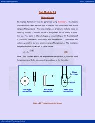
4.6 Switching <strong>Characteristics</strong> of a Thyristor<br />
During Turn on and Turn off process a thyristor is subjected to different voltages across it and<br />
different currents through it. The time variations of the voltage across a thyristor and the current<br />
through it during Turn on and Turn off constitute the switching characteristics of a thyristor.<br />
4.6.1 Turn on Switching <strong>Characteristics</strong><br />
A forward biased thyristor is turned on by applying a positive gate voltage between the gate and<br />
cathode as shown in Fig 4.10.<br />
+ -<br />
v AK<br />
i g<br />
V i<br />
i g<br />
i A<br />
R<br />
v<br />
i A<br />
AK<br />
t<br />
0.9 I ON<br />
I ON<br />
0.1 I<br />
Firing angle<br />
ON<br />
t<br />
α V i<br />
v AK<br />
i A<br />
0.9 V ON<br />
V ON<br />
0.1 V<br />
Expanded scale<br />
ON<br />
t<br />
t ON<br />
t d t r t p<br />
Fig. 4.10: Turn on characteristics of a thyristor.<br />
Fig 4.10 shows the waveforms of the gate current (i g ), anode current (i A ) and anode cathode<br />
voltage (V AK ) in an expanded time scale during Turn on. The reference circuit and the associated<br />
waveforms are shown in the inset. The total switching period being much smaller compared to<br />
the cycle time, i A and V AK before and after switching will appear flat.<br />
As shown in Fig 4.10 there is a transition time “t ON ” from forward off state to forward on state.<br />
This transition time is called the thyristor turn of time and can be divided into three separate<br />
intervals namely, (i) delay time (t d ) (ii) rise time (t r ) and (iii) spread time (t p ). These times are<br />
shown in Fig 4.10 for a resistive load.<br />
Version 2 EE IIT, Kharagpur 18