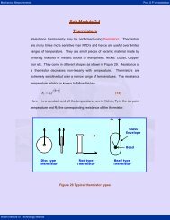
Characteristics: Triac - nptel
Characteristics: Triac - nptel
Characteristics: Triac - nptel

Create successful ePaper yourself
Turn your PDF publications into a flip-book with our unique Google optimized e-Paper software.
The left hand side of Fig 4.3 shows the reverse i-v characteristics of the thyristor. Once the<br />
thyristor is ON the only way to turn it OFF is by bringing the thyristor current below holding<br />
current (I H ). The gate terminal has no control over the turn OFF process. In ac circuits with<br />
resistive load this happens automatically during negative zero crossing of the supply voltage.<br />
This is called “natural commutation” or “line commutation”. However, in dc circuits some<br />
arrangement has to be made to ensure this condition. This process is called “forced<br />
commutation.”<br />
During reverse blocking if i g = 0 then only reverse saturation current (I s ) flows until the reverse<br />
voltage reaches reverse break down voltage (V BRR ). At this point current starts rising sharply.<br />
Large reverse voltage and current generates excessive heat and destroys the device. If i g > 0<br />
during reverse bias condition the reverse saturation current rises as explained in the previous<br />
section. This can be avoided by removing the gate current while the thyristor is reverse biased.<br />
The static output i-v characteristics of a thyristor depends strongly on the junction temperature as<br />
shown in Fig 4.4.<br />
V BRF<br />
I A<br />
T j =<br />
150° 135° 25° 75° 125°<br />
25° 75° 125° 150° T j<br />
V AK<br />
T j = 125° 75° 25° 135° 150°<br />
Fig. 4.4: Effect of junction temperature (T j ) on the output<br />
i – v characteristics of a thyristor.<br />
4.4.2 Thyristor Gate <strong>Characteristics</strong><br />
The gate circuit of a thyristor behaves like a poor quality diode with high on state voltage drop<br />
and low reverse break down voltage. This characteristic usually is not unique even within the<br />
same family of devices and shows considerable variation from device to device. Therefore,<br />
manufacturer’s data sheet provides the upper and lower limit of this characteristic as shown in<br />
Fig 4.5.<br />
Version 2 EE IIT, Kharagpur 10