ICL7136 - igor
ICL7136 - igor
ICL7136 - igor

Create successful ePaper yourself
Turn your PDF publications into a flip-book with our unique Google optimized e-Paper software.
TM<br />
<strong>ICL7136</strong><br />
Data Sheet May 2001<br />
File Number 3086.4<br />
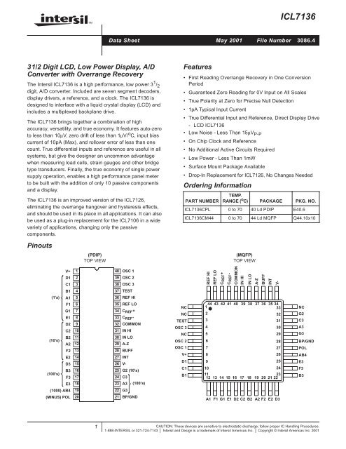
31/2 Digit LCD, Low Power Display, A/D<br />
Converter with Overrange Recovery<br />
The Intersil <strong>ICL7136</strong> is a high performance, low power 3 1 / 2<br />
digit, A/D converter. Included are seven segment decoders,<br />
display drivers, a reference, and a clock. The <strong>ICL7136</strong> is<br />
designed to interface with a liquid crystal display (LCD) and<br />
includes a multiplexed backplane drive.<br />
The <strong>ICL7136</strong> brings together a combination of high<br />
accuracy, versatility, and true economy. It features auto-zero<br />
to less than 10µV, zero drift of less than 1µV/ o C, input bias<br />
current of 10pA (Max), and rollover error of less than one<br />
count. True differential inputs and reference are useful in all<br />
systems, but give the designer an uncommon advantage<br />
when measuring load cells, strain gauges and other bridge<br />
type transducers. Finally, the true economy of single power<br />
supply operation, enables a high performance panel meter<br />
to be built with the addition of only 10 passive components<br />
and a display.<br />
The <strong>ICL7136</strong> is an improved version of the ICL7126,<br />
eliminating the overrange hangover and hysteresis effects,<br />
and should be used in its place in all applications. It can also<br />
be used as a plug-in replacement for the ICL7106 in a wide<br />
variety of applications, changing only the passive<br />
components.<br />
Features<br />
• First Reading Overrange Recovery in One Conversion<br />
Period<br />
• Guaranteed Zero Reading for 0V Input on All Scales<br />
• True Polarity at Zero for Precise Null Detection<br />
• 1pA Typical Input Current<br />
• True Differential Input and Reference, Direct Display Drive<br />
- LCD <strong>ICL7136</strong><br />
• Low Noise - Less Than 15µV P-P<br />
• On Chip Clock and Reference<br />
• No Additional Active Circuits Required<br />
• Low Power - Less Than 1mW<br />
• Surface Mount Package Available<br />
• Drop-In Replacement for ICL7126, No Changes Needed<br />
Ordering Information<br />
PART NUMBER<br />
TEMP.<br />
RANGE ( o C) PACKAGE PKG. NO.<br />
<strong>ICL7136</strong>CPL 0 to 70 40 Ld PDIP E40.6<br />
<strong>ICL7136</strong>CM44 0 to 70 44 Ld MQFP Q44.10x10<br />
Pinouts<br />
(PDIP)<br />
TOP VIEW<br />
(MQFP)<br />
TOP VIEW<br />
V+<br />
D1<br />
C1<br />
1<br />
2<br />
3<br />
40<br />
39<br />
38<br />
OSC 1<br />
OSC 2<br />
OSC 3<br />
REF HI<br />
REF LO<br />
C REF +<br />
C REF -<br />
COMMON<br />
IN HI<br />
IN LO<br />
A-Z<br />
BUFF<br />
INT<br />
V-<br />
B1<br />
4<br />
37<br />
TEST<br />
(1’s)<br />
A1<br />
5<br />
36<br />
REF HI<br />
(10’s)<br />
(100’s)<br />
F1<br />
G1<br />
E1<br />
D2<br />
C2<br />
B2<br />
A2<br />
F2<br />
E2<br />
D3<br />
B3<br />
F3<br />
E3<br />
6<br />
7<br />
8<br />
9<br />
10<br />
11<br />
12<br />
13<br />
14<br />
15<br />
16<br />
17<br />
18<br />
35<br />
34<br />
33<br />
32<br />
31<br />
30<br />
29<br />
28<br />
27<br />
26<br />
25<br />
24<br />
23<br />
REF LO<br />
C REF +<br />
C REF -<br />
COMMON<br />
IN HI<br />
IN LO<br />
A-Z<br />
BUFF<br />
INT<br />
V-<br />
G2 (10’s)<br />
C3<br />
A3 (100’s)<br />
NC<br />
44 43 42 41 40<br />
1<br />
39 38 37 36 35 34<br />
33<br />
NC<br />
TEST<br />
OSC 3<br />
NC<br />
OSC 2<br />
OSC 1<br />
V+<br />
D1<br />
C1<br />
2<br />
3<br />
4<br />
5<br />
6<br />
7<br />
8<br />
9<br />
10<br />
32<br />
31<br />
30<br />
29<br />
28<br />
27<br />
26<br />
25<br />
24<br />
B1 11<br />
12 13 14 15 16 17 18 19<br />
23<br />
20 21 22<br />
NC<br />
G2<br />
C3<br />
A3<br />
G3<br />
BP/GND<br />
POL<br />
AB4<br />
E3<br />
F3<br />
B3<br />
(1000) AB4<br />
19<br />
22<br />
G3<br />
(MINUS) POL<br />
20<br />
21<br />
BP/GND<br />
A1 F1 G1 E1 D2 C2 B2 A2 F2 E2 D3<br />
1<br />
CAUTION: These devices are sensitive to electrostatic discharge; follow proper IC Handling Procedures.<br />
1-888-INTERSIL or 321-724-7143 | Intersil and Design is a trademark of Intersil Americas Inc. | Copyright © Intersil Americas Inc. 2001
<strong>ICL7136</strong><br />
Absolute Maximum Ratings<br />
Supply Voltage<br />
<strong>ICL7136</strong>,V+toV-...................................15V<br />
Analog Input Voltage (Either Input) (Note 1) . . . . . . . . . . . . V+ to V-<br />
ReferenceInputVoltage(EitherInput)................. V+toV-<br />
Clock Input<br />
<strong>ICL7136</strong>................................... TESTtoV+<br />
Operating Conditions<br />
TemperatureRange............................0 o Cto70 o C<br />
Thermal Information<br />
Thermal Resistance (Typical, Note 2)<br />
θ JA ( o C/W)<br />
PDIPPackage............................. 50<br />
MQFPPackage............................ 75<br />
MaximumJunctionTemperature.......................150 o C<br />
MaximumStorageTemperatureRange.......... -65 o Cto150 o C<br />
Maximum Lead Temperature (Soldering 10s) . . . . . . . . . . . . .300 o C<br />
(MQFP - Lead Tips Only)<br />
CAUTION: Stresses above those listed in “Absolute Maximum Ratings” may cause permanent damage to the device. This is a stress only rating and operation ofthe<br />
device at these or any other conditions above those indicated in the operational sections of this specification is not implied.<br />
NOTES:<br />
1. Input voltages may exceed the supply voltages provided the input current is limited to ±100µA.<br />
2. θ JA is measured with the component mounted on a low effective thermal conductivity test board in free air. See Tech Brief TB379 for details.<br />
Electrical Specifications (Note 3)<br />
SYSTEM PERFORMANCE<br />
PARAMETER TEST CONDITIONS MIN TYP MAX UNITS<br />
Zero Input Reading V IN = 0V, Full Scale = 200mV -000.0 ±000.0 +000.0 Digital<br />
Reading<br />
Ratiometric Reading V lN =V REF ,V REF = 100mV 999 999/<br />
1000<br />
1000 Digital<br />
Reading<br />
Rollover Error<br />
Linearity<br />
-V IN =+V lN ≅ 200mV Difference in Reading for Equal Positive<br />
and Negative Inputs Near Full Scale<br />
Full Scale = 200mV or Full Scale = 2V Maximum<br />
Deviation from Best Straight Line Fit (Note 5)<br />
- ±0.2 ±1 Counts<br />
- ±0.2 ±1 Counts<br />
Common Mode Rejection Ratio V CM = ±1V, V IN = 0V, Full Scale = 200mV (Note 5) - 50 - µV/V<br />
Noise<br />
V IN = 0V, Full Scale = 200mV (Peak-To-Peak Value Not<br />
Exceeded 95% of Time) (Note 5)<br />
- 15 - µV<br />
Leakage Current Input V lN = 0V (Note 5) - 1 10 pA<br />
Zero Reading Drift V lN =0V,0 o CTo70 o C (Note 5) - 0.2 1 µV/ o C<br />
Scale Factor Temperature Coefficient V IN = 199mV, 0 o CTo70 o C, (Ext. Ref. 0ppm/× o C) (Note 5) - 1 5 ppm/ o C<br />
COMMON Pin Analog Common Voltage<br />
Temperature Coefficient of Analog<br />
Common<br />
SUPPLY CURRENT<br />
25kΩ Between Common and Positive Supply (With Respect<br />
to + Supply)<br />
25kΩ Between Common and Positive Supply (With Respect<br />
to + Supply) (Note 5)<br />
2.4 3.0 3.2 V<br />
- 150 - ppm/ o C<br />
V+ Supply Current V IN = 0 (Does Not Include Common Current) 16kHz<br />
Oscillator (Note 6)<br />
- 70 100 µA<br />
DISPLAY DRIVER<br />
Peak-To-Peak Segment Drive Voltage and<br />
Peak-To-Peak Backplane Drive Voltage<br />
V+ to V- = 9V (Note 4) 4 5.5 6 V<br />
NOTES:<br />
3. Unless otherwise noted, specifications apply to the <strong>ICL7136</strong> at T A =25 o C, f CLOCK = 48kHz. <strong>ICL7136</strong> is tested in the circuit of Figure 1.<br />
4. Back plane drive is in phase with segment drive for “off“ segment, 180 degrees out of phase for “on“ segment. Frequency is 20 times conversion<br />
rate. Average DC component is less than 50mV.<br />
5. Not tested, guaranteed by design.<br />
6. 48kHz oscillator increases current by 20µA (Typ).<br />
2
<strong>ICL7136</strong><br />
Typical Applications and Test Circuits<br />
+ -<br />
IN<br />
+<br />
9V<br />
-<br />
R 5<br />
R 2<br />
R 1<br />
C<br />
R C 5<br />
4 1 C 2 C 3<br />
R 3 C 4<br />
DISPLAY<br />
40<br />
39<br />
38<br />
37<br />
36<br />
35<br />
34<br />
33<br />
32<br />
31<br />
30<br />
29<br />
28<br />
27<br />
26<br />
25<br />
24<br />
23<br />
22<br />
OSC 1<br />
OSC 2<br />
OSC 3<br />
TEST<br />
REF HI<br />
REF LO<br />
C REF +<br />
C REF -<br />
COM<br />
IN HI<br />
IN LO<br />
A-Z<br />
BUFF<br />
INT<br />
V-<br />
G2<br />
C3<br />
A3<br />
G3<br />
<strong>ICL7136</strong><br />
V+<br />
D1<br />
C1<br />
B1<br />
A1<br />
F1<br />
G1<br />
E1<br />
D2<br />
C2<br />
B2<br />
A2<br />
F2<br />
E2<br />
D3<br />
B3<br />
F3<br />
E3<br />
AB4<br />
1<br />
2<br />
3<br />
4<br />
5<br />
6<br />
7<br />
8<br />
9<br />
10<br />
11<br />
12<br />
13<br />
14<br />
15<br />
16<br />
17<br />
18<br />
19<br />
DISPLAY<br />
20 POL<br />
BP 21<br />
C 1 =0.1µF<br />
C 2 =0.47µF<br />
C 3 =0.047µF<br />
C 4 =50pF<br />
C 5 =0.01µF<br />
R 1 =240kΩ<br />
R 2 =180kΩ<br />
R 3 =180kΩ<br />
R 4 =10kΩ<br />
R 5 =1MΩ<br />
FIGURE 1. <strong>ICL7136</strong> TEST CIRCUIT AND TYPICAL APPLICATION WITH LCD DISPLAY COMPONENTS SELECTED FOR 200mV FULL SCALE<br />
3
<strong>ICL7136</strong><br />
Design Information Summary Sheet<br />
• OSCILLATOR FREQUENCY<br />
f OSC =0.45/RC<br />
C OSC > 50pF; R OSC > 50kΩ<br />
f OSC (Typ) = 48kHz<br />
• OSCILLATOR PERIOD<br />
t OSC = RC/0.45<br />
• INTEGRATION CLOCK FREQUENCY<br />
f CLOCK =f OSC /4<br />
• INTEGRATION PERIOD<br />
t INT = 1000 x (4/f OSC )<br />
• 60/50Hz REJECTION CRITERION<br />
t INT /t 60Hz or t lNT /t 50Hz = Integer<br />
• OPTIMUM INTEGRATION CURRENT<br />
I INT =1µA<br />
• FULL SCALE ANALOG INPUT VOLTAGE<br />
V lNFS (Typ)=200mVor2V<br />
• INTEGRATE RESISTOR<br />
V INFS<br />
R INT = ----------------<br />
I INT<br />
• INTEGRATE CAPACITOR<br />
( t INT )( I INT )<br />
C INT = -------------------------------<br />
V INT<br />
• INTEGRATOR OUTPUT VOLTAGE SWING<br />
( t INT<br />
)( I INT<br />
)<br />
V INT = -------------------------------<br />
C INT<br />
• DISPLAY COUNT<br />
V IN<br />
COUNT = 1000 × --------------<br />
V REF<br />
• CONVERSION CYCLE<br />
t CYC =t CL0CK x 4000<br />
t CYC =t OSC x16,000<br />
when f OSC =48kHz;t CYC =333ms<br />
• COMMON MODE INPUT VOLTAGE<br />
(V-+1V)
<strong>ICL7136</strong><br />
Pin Descriptions<br />
PIN NUMBER<br />
44 PIN<br />
40 PIN DIP FLATPACK NAME FUNCTION DESCRIPTION<br />
1 8 V+ Supply Power Supply.<br />
2 9 D1 Output Driver Pin for Segment “D” of the display units digit.<br />
3 10 C1 Output Driver Pin for Segment “C” of the display units digit.<br />
4 11 B1 Output Driver Pin for Segment “B” of the display units digit.<br />
5 12 A1 Output Driver Pin for Segment “A” of the display units digit.<br />
6 13 F1 Output Driver Pin for Segment “F” of the display units digit.<br />
7 14 G1 Output Driver Pin for Segment “G” of the display units digit.<br />
8 15 E1 Output Driver Pin for Segment “E” of the display units digit.<br />
9 16 D2 Output Driver Pin for Segment “D” of the display tens digit.<br />
10 17 C2 Output Driver Pin for Segment “C” of the display tens digit.<br />
11 18 B2 Output Driver Pin for Segment “B” of the display tens digit.<br />
12 19 A2 Output Driver Pin for Segment “A” of the display tens digit.<br />
13 20 F2 Output Driver Pin for Segment “F” of the display tens digit.<br />
14 21 E2 Output Driver Pin for Segment “E” of the display tens digit.<br />
15 22 D3 Output Driver pin for segment “D” of the display hundreds digit.<br />
16 23 B3 Output Driver pin for segment “B” of the display hundreds digit.<br />
17 24 F3 Output Driver pin for segment “F” of the display hundreds digit.<br />
18 25 E3 Output Driver pin for segment “E” of the display hundreds digit.<br />
19 26 AB4 Output Driver pin for both “A” and “B” segments of the display thousands digit.<br />
20 27 POL Output Driver pin for the negative sign of the display.<br />
21 28 BP/GND Output Driver pin for the LCD backplane/Power Supply Ground.<br />
22 29 G3 Output Driver pin for segment “G” of the display hundreds digit.<br />
23 30 A3 Output Driver pin for segment “A” of the display hundreds digit.<br />
24 31 C3 Output Driver pin for segment “C” of the display hundreds digit.<br />
25 32 G2 Output Driver pin for segment “G” of the display tens digit.<br />
26 34 V - Supply Negative power supply.<br />
27 35 INT Output Integrator amplifier output. To be connected to integrating capacitor.<br />
28 36 BUFF Output Input buffer amplifier output. To be connected to integrating resistor.<br />
29 37 A-Z Input Integrator amplifier input. To be connected to auto-zero capacitor.<br />
30<br />
31<br />
38<br />
39<br />
IN LO<br />
IN HI<br />
Input<br />
32 40 COMMON Supply/<br />
Output<br />
33<br />
34<br />
35<br />
36<br />
41<br />
42<br />
43<br />
44<br />
C REF -<br />
C REF +<br />
REF LO<br />
REF HI<br />
Input<br />
Differential inputs. To be connected to input voltage to be measured. LO and HI<br />
designators are for reference and do not imply that LO should be connected to lower<br />
potential, e.g., for negative inputs IN LO has a higher potential than IN HI.<br />
Internal voltage reference output.<br />
Connection pins for reference capacitor.<br />
Input pins for reference voltage to the device. REF HI should be positive reference to<br />
REF LO.<br />
37 3 TEST Input Display test. Turns on all segments when tied to V+.<br />
38<br />
39<br />
40<br />
4<br />
6<br />
7<br />
OSC3<br />
OSC2<br />
OSC1<br />
Output<br />
Output<br />
Input<br />
Device clock generator circuit connection pins.<br />
Detailed Description<br />
Analog Section<br />
Figure 2 shows the Analog Section for the <strong>ICL7136</strong>. Each<br />
measurement cycle is divided into four phases. They are (1)<br />
auto-zero (A-Z), (2) signal integrate (INT) and (3) deintegrate<br />
(DE), (4) zero integrate (ZI).<br />
Auto-Zero Phase<br />
During auto-zero three things happen. First, input high and low<br />
are disconnected from the pins and internally shorted to analog<br />
COMMON. Second, the reference capacitor is charged to the<br />
reference voltage. Third, a feedback loop is closed around the<br />
system to charge the auto-zero capacitor C AZ to compensate<br />
for offset voltages in the buffer amplifier, integrator, and<br />
comparator. Since the comparator is included in the loop, the A-<br />
Z accuracy is limited only by the noise of the system. In any<br />
case, the offset referred to the input is less than 10µV.<br />
Signal Integrate Phase<br />
During signal integrate, the auto-zero loop is opened, the<br />
internal short is removed, and the internal input high and low<br />
5
<strong>ICL7136</strong><br />
are connected to the external pins. The converter then<br />
integrates the differential voltage between IN HI and IN LO<br />
for a fixed time. This differential voltage can be within a wide<br />
common mode range: up to 1V from either supply. If, on the<br />
other hand, the input signal has no return with respect to the<br />
converter power supply, IN LO can be tied to analog<br />
COMMON to establish the correct common mode voltage. At<br />
the end of this phase, the polarity of the integrated signal is<br />
determined.<br />
De-Integrate Phase<br />
The final phase is de-integrate, or reference integrate. Input<br />
low is internally connected to analog COMMON and input<br />
high is connected across the previously charged reference<br />
capacitor. Circuitry within the chip ensures that the capacitor<br />
will be connected with the correct polarity to cause the<br />
integrator output to return to zero. The time required for the<br />
output to return to zero is proportional to the input signal.<br />
Specifically the digital reading displayed is:<br />
⎛<br />
DISPLAY READING = 1000<br />
V IN ⎞<br />
⎜--------------<br />
⎟ .<br />
⎝V REF ⎠<br />
Zero Integrator Phase<br />
The final phase is zero integrator. First, input low is shorted to<br />
analog COMMON. Second, the reference capacitor is charged<br />
to the reference voltage. Finally, a feedback loop is closed<br />
around the system to IN HI to cause the integrator output to<br />
return to zero. Under normal conditions, this phase lasts for<br />
between 11 to 140 clock pulses, but after a “heavy” overrange<br />
conversion, it is extended to 740 clock pulses.<br />
Differential Input<br />
The input can accept differential voltages anywhere within the<br />
common mode range of the input amplifier, or specifically from<br />
0.5V below the positive supply to 1V above the negative supply.<br />
In this range, the system has a CMRR of 86dB typical.<br />
However, care must be exercised to assure the integrator<br />
output does not saturate. A worst case condition would be a<br />
large positive common mode voltage with a near full scale<br />
negative differential input voltage. The negative input signal<br />
drives the integrator positive when most of its swing has been<br />
used up by the positive common mode voltage. For these<br />
critical applications the integrator output swing can be reduced<br />
to less than the recommended 2V full scale swing with little loss<br />
of accuracy. The integrator output can swing to within 0.3V of<br />
either supply without loss of linearity.<br />
Differential Reference<br />
The reference voltage can be generated anywhere within the<br />
power supply voltage of the converter. The main source of<br />
common mode error is a roll-over voltage caused by the<br />
reference capacitor losing or gaining charge to stray capacity<br />
on its nodes. If there is a large common mode voltage, the<br />
reference capacitor can gain charge (increase voltage) when<br />
called up to de-integrate a positive signal but lose charge<br />
(decrease voltage) when called up to de-integrate a negative<br />
input signal. This difference in reference for positive or<br />
negative input voltage will give a roll-over error. However, by<br />
selecting the reference capacitor such that it is large enough<br />
in comparison to the stray capacitance, this error can be<br />
held to less than 0.5 count worst case. (See Component<br />
Value Selection.)<br />
STRAY<br />
C REF<br />
STRAY<br />
R INT<br />
C AZ<br />
C INT<br />
C REF<br />
+<br />
REF HI<br />
REF LO<br />
C REF -<br />
BUFFER<br />
V+<br />
A-Z<br />
INT<br />
V+<br />
34<br />
36<br />
35<br />
33<br />
28 1 29 27<br />
IN HI<br />
31<br />
10µA<br />
A-Z,<br />
ZI<br />
A-Z,<br />
ZI<br />
-<br />
+<br />
2.8V<br />
INTEGRATOR<br />
-<br />
+<br />
-<br />
+<br />
TO<br />
DIGITAL<br />
SECTION<br />
INT<br />
DE-<br />
DE+<br />
INPUT<br />
HIGH<br />
6.2V<br />
A-Z<br />
COMMON<br />
IN LO<br />
32<br />
30<br />
INT<br />
A-Z<br />
DE+ DE-<br />
A-Z AND DE(±)<br />
AND ZI<br />
N<br />
26<br />
-<br />
+<br />
ZI<br />
INPUT<br />
LOW<br />
COMPARATOR<br />
V-<br />
FIGURE 2. ANALOG SECTION OF <strong>ICL7136</strong><br />
6
<strong>ICL7136</strong><br />
Analog COMMON<br />
This pin is included primarily to set the common mode<br />
voltage for battery operation or for any system where the<br />
input signals are floating with respect to the power supply.<br />
The COMMON pin sets a voltage that is approximately 2.8V<br />
more negative than the positive supply. This is selected to<br />
give a minimum end-of-life battery voltage of about 6.8V.<br />
However, analog COMMON has some of the attributes of a<br />
reference voltage. When the total supply voltage is large<br />
enough to cause the zener to regulate (>7V), the COMMON<br />
voltage will have a low voltage coefficient (0.001%/V), low<br />
output impedance (≅15Ω), and a temperature coefficient<br />
typically less than 150ppm/ o C.<br />
V+<br />
V<br />
REF HI<br />
REF LO<br />
<strong>ICL7136</strong><br />
V-<br />
FIGURE 3A.<br />
6.8V<br />
ZENER<br />
I Z<br />
The limitations of the on chip reference should also be<br />
recognized, however. Due to their higher thermal resistance,<br />
plastic parts are poorer in this respect than ceramic. The<br />
combination of reference Temperature Coefficient (TC), internal<br />
chip dissipation, and package thermal resistance can increase<br />
noise near full scale from 25µV to80µV P-P . Also the linearity in<br />
going from a high dissipation count such as 1000 (20 segments<br />
on) to a low dissipation count such as 1111 (8 segments on)<br />
can suffer by a count or more. Devices with a positive TC<br />
reference may require several counts to pull out of an over<br />
range condition. This is because over-range is a low dissipation<br />
mode, with the three least significant digits blanked. Similarly,<br />
units with a negative TC may cycle between over range and a<br />
non-over range count as the die alternately heats and cools. All<br />
these problems are of course eliminated if an external<br />
reference is used.<br />
The <strong>ICL7136</strong>, with its negligible dissipation, suffers from<br />
none of these problems. In either case, an external<br />
reference can easily be added, as shown in Figure 3.<br />
Analog COMMON is also used as the input low return during<br />
auto-zero and de-integrate. If IN LO is different from analog<br />
COMMON, a common mode voltage exists in the system<br />
and is taken care of by the excellent CMRR of the converter.<br />
However, in some applications IN LO will be set at a fixed<br />
known voltage (power supply common for instance). In this<br />
application, analog COMMON should be tied to the same<br />
point, thus removing the common mode voltage from the<br />
converter. The same holds true for the reference voltage. If<br />
reference can be conveniently tied to analog COMMON, it<br />
should be since this removes the common mode voltage<br />
from the reference system.<br />
Within the lC, analog COMMON is tied to an N-Channel FET<br />
that can sink approximately 3mA of current to hold the<br />
voltage 2.8V below the positive supply (when a load is trying<br />
to pull the common line positive). However, there is only<br />
10µA of source current, so COMMON may easily be tied to a<br />
more negative voltage thus overriding the internal reference.<br />
V<br />
<strong>ICL7136</strong><br />
REF HI<br />
REF LO<br />
COMMON<br />
20kΩ<br />
TEST<br />
The TEST pin serves two functions. On the <strong>ICL7136</strong> it is<br />
coupled to the internally generated digital supply through a<br />
500Ω resistor. Thus it can be used as the negative supply for<br />
externally generated segment drivers such as decimal points<br />
or any other presentation the user may want to include on<br />
the LCD display. Figures 4 and 5 show such an application.<br />
No more than a 1mA load should be applied.<br />
The second function is a “lamp test”. When TEST is pulled<br />
high (to V+) all segments will be turned on and the display<br />
should read “-1888”. The TEST pin will sink about 5mA<br />
under these conditions.<br />
V+<br />
6.8kΩ<br />
ICL8069<br />
1.2V<br />
REFERENCE<br />
FIGURE 3B.<br />
FIGURE 3. USING AN EXTERNAL REFERENCE<br />
V+<br />
<strong>ICL7136</strong><br />
BP<br />
TEST<br />
21<br />
1MΩ<br />
TO LCD<br />
DECIMAL<br />
POINT<br />
37 TO LCD<br />
BACKPLANE<br />
FIGURE 4. SIMPLE INVERTER FOR FIXED DECIMAL POINT<br />
CAUTION: On the <strong>ICL7136</strong>, in the lamp test mode, the segments have a<br />
constant DC voltage (no square-wave) and may burn the LCD<br />
display if left in this mode for several minutes.<br />
7
<strong>ICL7136</strong><br />
V+<br />
<strong>ICL7136</strong><br />
TEST<br />
BP<br />
DECIMAL<br />
POINT<br />
SELECT<br />
V+<br />
CD4030<br />
GND<br />
TO LCD<br />
DECIMAL<br />
POINTS<br />
FIGURE 5. EXCLUSIVE “OR” GATE FOR DECIMAL POINT DRIVE<br />
Digital Section<br />
Figures 6 shows the digital section for the <strong>ICL7136</strong>. In the<br />
<strong>ICL7136</strong>, an internal digital ground is generated from a 6V<br />
Zener diode and a large P-Channel source follower. This<br />
supply is made stiff to absorb the relatively large capacitive<br />
currents when the back plane (BP) voltage is switched. The<br />
BP frequency is the clock frequency divided by 800. For<br />
three readings/second this is a 60Hz square wave with a<br />
nominal amplitude of 5V. The segments are driven at the<br />
same frequency and amplitude and are in phase with BP<br />
when OFF, but out of phase when ON. In all cases negligible<br />
DC voltage exists across the segments.<br />
The polarity indication is “on” for negative analog inputs. If IN<br />
LO and IN HI are reversed, this indication can be reversed<br />
also, if desired.<br />
b<br />
a<br />
e<br />
f<br />
a<br />
b<br />
g<br />
c<br />
c<br />
d<br />
e<br />
f<br />
a<br />
b<br />
g<br />
c<br />
d<br />
e<br />
f<br />
a<br />
b<br />
g<br />
c<br />
d<br />
BACKPLANE<br />
21<br />
LCD PHASE DRIVER<br />
TYPICAL SEGMENT OUTPUT<br />
V+<br />
0.5mA<br />
2mA<br />
SEGMENT<br />
OUTPUT<br />
INTERNAL DIGITAL GROUND<br />
7<br />
SEGMENT<br />
DECODE<br />
LATCH<br />
7<br />
SEGMENT<br />
DECODE<br />
7<br />
SEGMENT<br />
DECODE<br />
1000’s 100’s 10’s 1’s<br />
COUNTER COUNTER COUNTER COUNTER<br />
÷200<br />
† THREE INVERTERS<br />
ONLY ONE INVERTER SHOWN<br />
FOR CLARITY<br />
TO SWITCH DRIVERS<br />
FROM COMPARATOR OUTPUT<br />
†<br />
CLOCK<br />
÷4<br />
INTERNAL<br />
DIGITAL<br />
GROUND<br />
LOGIC CONTROL<br />
V TH =1V<br />
1<br />
6.2V<br />
500Ω<br />
37<br />
V+<br />
TEST<br />
40 39 38<br />
26<br />
V-<br />
OSC 1 OSC 2 OSC 3<br />
FIGURE 6. <strong>ICL7136</strong> DIGITAL SECTION<br />
8
<strong>ICL7136</strong><br />
System Timing<br />
Figure 7 shows the clocking arrangement used in the<br />
<strong>ICL7136</strong>. Two basic clocking arrangements can be used:<br />
1. Figure 9A, an external oscillator connected to DIP pin 40.<br />
2. Figure 9B, an R-C oscillator using all three pins.<br />
The oscillator frequency is divided by four before it clocks the<br />
decade counters. It is then further divided to form the three<br />
convert-cycle phases. These are signal integrate (1000<br />
counts), reference de-integrate (0 to 2000 counts) and autozero<br />
(1000 to 3000 counts). For signals less than full scale,<br />
auto-zero gets the unused portion of reference de-integrate.<br />
This makes a complete measure cycle of 4,000 counts<br />
(16,000 clock pulses) independent of input voltage. For three<br />
readings/second, an oscillator frequency of 48kHz would be<br />
used.<br />
To achieve maximum rejection of 60Hz pickup, the signal<br />
integrate cycle should be a multiple of 60Hz. Oscillator<br />
frequencies of 240kHz, 120kHz, 80kHz, 60kHz, 48kHz,<br />
40kHz, 33 1 / 3 kHz, etc., should be selected. For 50Hz<br />
rejection, Oscillator frequencies of 200kHz, 100kHz,<br />
66 2 / 3 kHz, 50kHz, 40kHz, etc. would be suitable. Note that<br />
40kHz (2.5 readings/sec.) will reject both 50Hz and 60Hz<br />
(also 400Hz and 440Hz).<br />
TEST<br />
INTERNAL TO PART<br />
40 39 38<br />
÷4<br />
FIGURE 7A. EXTERNAL OSCILLATOR<br />
INTERNAL TO PART<br />
40 39 38<br />
R<br />
÷4<br />
FIGURE 7B. RC OSCILLATOR<br />
FIGURE 7. CLOCK CIRCUITS<br />
C<br />
CLOCK<br />
CLOCK<br />
Component Value Selection<br />
Integrating Resistor<br />
Both the buffer amplifier and the integrator have a class A<br />
output stage with 100µA of quiescent current. They can<br />
supply 1µA of drive current with negligible nonlinearity. The<br />
integrating resistor should be large enough to remain in this<br />
very linear region over the input voltage range, but small<br />
enough that undue leakage requirements are not placed on<br />
the PC board. For 2V full scale, 1.8MΩ is near optimum and<br />
similarly a 180kΩ for a 200mV scale.<br />
Integrating Capacitor<br />
The integrating capacitor should be selected to give the<br />
maximum voltage swing that ensures tolerance buildup will<br />
not saturate the integrator swing (approximately 0.3V from<br />
either supply). In the <strong>ICL7136</strong>, when the analog COMMON<br />
is used as a reference, a nominal +2V full-scale integrator<br />
swing is fine. For three readings/second (48kHz clock)<br />
nominal values for C lNT are 0.047µF and 0.5µF, respectively.<br />
Of course, if different oscillator frequencies are used, these<br />
values should be changed in inverse proportion to maintain<br />
the same output swing.<br />
An additional requirement of the integrating capacitor is that<br />
it must have a low dielectric absorption to prevent roll-over<br />
errors. While other types of capacitors are adequate for this<br />
application, polypropylene capacitors give undetectable<br />
errors at reasonable cost.<br />
Auto-Zero Capacitor<br />
The size of the auto-zero capacitor has some influence on<br />
the noise of the system. For 200mV full scale where noise is<br />
very important, a 0.47µF capacitor is recommended. On the<br />
2V scale, a 0.047µF capacitor increases the speed of<br />
recovery from overload and is adequate for noise on this<br />
scale.<br />
Reference Capacitor<br />
A0.1µF capacitor gives good results in most applications.<br />
However, where a large common mode voltage exists (i.e.,<br />
the REF LO pin is not at analog COMMON) and a 200mV<br />
scale is used, a larger value is required to prevent roll-over<br />
error. Generally 1µF will hold the roll-over error to 0.5 count<br />
in this instance.<br />
Oscillator Components<br />
For all ranges of frequency a 180kΩ resistor is<br />
recommended and the capacitor is selected from the<br />
equation:<br />
f<br />
0.45<br />
= ------------ For 48kHz Clock (3 Readings/s.),<br />
RC<br />
C<br />
= 50pF.<br />
9
<strong>ICL7136</strong><br />
Reference Voltage<br />
The analog input required to generate full scale output (2000<br />
counts) is: V lN =2V REF . Thus, for the 200mV and 2V scale,<br />
V REF should equal 100mV and 1V, respectively. However, in<br />
many applications where the A/D is connected to a<br />
transducer, there will exist a scale factor other than unity<br />
between the input voltage and the digital reading. For<br />
instance, in a weighing system, the designer might like to<br />
have a full scale reading when the voltage from the<br />
transducer is 0.662V. Instead of dividing the input down to<br />
200mV, the designer should use the input voltage directly<br />
and select V REF = 0.341V. Suitable values for integrating<br />
resistor and capacitor would be 330kΩ and 0.047µF. This<br />
makes the system slightly quieter and also avoids a divider<br />
network on the input. Another advantage of this system<br />
occurs when a digital reading of zero is desired for V IN ≠ 0.<br />
Temperature and weighing systems with a variable fare are<br />
examples. This offset reading can be conveniently generated<br />
by connecting the voltage transducer between IN HI and<br />
COMMON and the variable (or fixed) offset voltage between<br />
COMMON and IN LO.<br />
Typical Applications<br />
The <strong>ICL7136</strong> may be used in a wide variety of<br />
configurations. The circuits which follow show some of the<br />
possibilities, and serve to illustrate the exceptional versatility<br />
of these A/D converters.<br />
The following application notes contain very useful<br />
information on understanding and applying this part and are<br />
available from Intersil.<br />
Application Notes<br />
NOTE #<br />
AN016<br />
AN017<br />
AN018<br />
AN023<br />
AN032<br />
AN046<br />
“Selecting A/D Converters”<br />
DESCRIPTION<br />
“The Integrating A/D Converter”<br />
“Do’s and Don’ts of Applying A/D Converters”<br />
“Low Cost Digital Panel Meter Designs”<br />
“Understanding the Auto-Zero and Common Mode<br />
Performance of the <strong>ICL7136</strong>/7/9 Family”<br />
“Building a Battery-Operated Auto Ranging DVM with<br />
the ICL7106”<br />
AN052<br />
“Tips for Using Single Chip 3 1 / 2 Digit A/D Converters”<br />
OSC 1<br />
OSC 2<br />
OSC 3<br />
TEST<br />
REF HI<br />
REF LO<br />
C REF<br />
C REF<br />
COMMON<br />
IN HI<br />
IN LO<br />
A-Z<br />
BUFF<br />
INT<br />
V-<br />
G2<br />
C3<br />
A3<br />
G3<br />
BP<br />
40<br />
39<br />
38<br />
37<br />
36<br />
35<br />
34<br />
33<br />
32<br />
31<br />
30<br />
29<br />
28<br />
27<br />
26<br />
25<br />
24<br />
23<br />
22<br />
21<br />
0.47µF<br />
0.047µF<br />
180kΩ<br />
50pF<br />
0.1µF<br />
180kΩ<br />
TO DISPLAY<br />
TO PIN 1<br />
20kΩ<br />
SET V REF<br />
= 100mV<br />
0.01µF<br />
240kΩ<br />
1MΩ<br />
TO BACKPLANE<br />
+<br />
IN<br />
-<br />
+<br />
9V<br />
-<br />
OSC 1<br />
OSC 2<br />
OSC 3<br />
TEST<br />
REF HI<br />
REF LO<br />
C REF<br />
C REF<br />
COMMON<br />
IN HI<br />
IN LO<br />
A-Z<br />
BUFF<br />
INT<br />
V-<br />
G2<br />
C3<br />
A3<br />
G3<br />
BP/GND<br />
40<br />
39<br />
38<br />
37<br />
36<br />
35<br />
34<br />
33<br />
32<br />
31<br />
30<br />
29<br />
28<br />
27<br />
26<br />
25<br />
24<br />
23<br />
22<br />
21<br />
0.01µF<br />
0.047µF<br />
180kΩ<br />
50pF<br />
0.1µF<br />
1.8M<br />
TO DISPLAY<br />
TO PIN 1<br />
SET V REF<br />
= 100mV<br />
250kΩ 240kΩ<br />
1MΩ<br />
0.01µF<br />
V+<br />
+<br />
IN<br />
-<br />
V-<br />
Values shown are for 200mV full scale, 3 readings/sec., floating<br />
supply voltage (9V battery).<br />
FIGURE 8. <strong>ICL7136</strong> USING THE INTERNAL REFERENCE<br />
FIGURE 9. RECOMMENDED COMPONENT VALUES FOR 2V<br />
FULL SCALE<br />
10
<strong>ICL7136</strong><br />
TO PIN 1<br />
OSC 1 40<br />
†<br />
OSC 2 39<br />
OSC 3 38<br />
SCALE<br />
TEST 37 50pF FACTOR<br />
ADJUST<br />
REF HI 36<br />
REF LO 35<br />
22kΩ<br />
C 34<br />
100kΩ 1MΩ<br />
REF<br />
0.1µF 200kΩ 470kΩ<br />
C REF 33<br />
COMMON 32<br />
IN HI 31<br />
ZERO SILICON NPN<br />
0.01µF ADJUST MPS 3704 OR<br />
IN LO 30<br />
SIMILAR<br />
0.47µF<br />
A-Z 29<br />
390kΩ<br />
+<br />
BUFF 28<br />
9V<br />
INT 27<br />
-<br />
†<br />
V- 26<br />
G2 25<br />
C3 24<br />
A3 23<br />
TO DISPLAY<br />
G3<br />
BP<br />
22<br />
21<br />
TO BACKPLANE<br />
A silicon diode-connected transistor has a temperature coefficient<br />
of about -2mV/ o C. Calibration is achieved by placing the sensing<br />
transistor in ice water and adjusting the zeroing potentiometer for a<br />
000.0 reading. The sensor should then be placed in boiling water<br />
and the scale-factor potentiometer adjusted for a 100.0 reading.<br />
† Value depends on clock frequency.<br />
FIGURE 10. <strong>ICL7136</strong> USED AS A DIGITAL CENTIGRADE<br />
THERMOMETER<br />
O /RANGE<br />
U /RANGE<br />
CD4023 OR<br />
74C10<br />
V+<br />
TO LOGIC<br />
V CC<br />
CD4077<br />
1 V+<br />
2 D1<br />
3 C1<br />
4 B1<br />
5 A1<br />
6 F1<br />
7 G1<br />
8 E1<br />
9 D2<br />
10 C2<br />
11 B2<br />
12 A2<br />
13 F2<br />
14 E2<br />
15 D3<br />
16 B3<br />
17 F3<br />
18 E3<br />
19 AB4<br />
20 POL<br />
OSC 1<br />
OSC 2<br />
OSC 3<br />
TEST<br />
REF HI<br />
REF LO<br />
C REF<br />
C REF<br />
COMMON<br />
IN HI<br />
IN LO<br />
A-Z<br />
BUFF<br />
INT<br />
V-<br />
G2<br />
C3<br />
A3<br />
G3<br />
BP<br />
40<br />
39<br />
38<br />
37<br />
36<br />
35<br />
34<br />
33<br />
32<br />
31<br />
30<br />
29<br />
28<br />
27<br />
26<br />
25<br />
24<br />
23<br />
22<br />
21<br />
TO<br />
LOGIC<br />
GND<br />
V-<br />
FIGURE 11. CIRCUIT FOR DEVELOPING UNDERRANGE AND<br />
OVERRANGE SIGNAL FROM <strong>ICL7136</strong> OUTPUTS<br />
OSC 1<br />
OSC 2<br />
OSC 3<br />
TEST<br />
REF HI<br />
REF LO<br />
C REF<br />
C REF<br />
40<br />
39<br />
38<br />
37<br />
36<br />
35<br />
34<br />
33<br />
TO PIN 1<br />
180kΩ<br />
50pF<br />
0.1µF<br />
20kΩ<br />
10µF<br />
220kΩ<br />
SCALE FACTOR ADJUST<br />
(V REF = 100mV FOR AC TO RMS)<br />
470kΩ<br />
1N914<br />
5µF CA3140<br />
2.2MΩ<br />
+<br />
-<br />
100kΩ<br />
AC IN<br />
COMMON<br />
IN HI<br />
IN LO<br />
A-Z<br />
BUFF<br />
INT<br />
V-<br />
32<br />
31<br />
30<br />
29<br />
28<br />
27<br />
26<br />
0.47µF<br />
180kΩ<br />
0.047µF<br />
10µF<br />
+<br />
9V<br />
-<br />
1µF<br />
4.3kΩ<br />
10kΩ<br />
100pF<br />
(FOR OPTIMUM<br />
BANDWIDTH)<br />
1µF<br />
10kΩ<br />
1µF<br />
0.22µF<br />
G2<br />
25<br />
C3<br />
A3<br />
24<br />
23<br />
TO DISPLAY<br />
G3<br />
22<br />
BP<br />
21<br />
TO BACKPLANE<br />
Test is used as a common-mode reference level to ensure compatibility with most op amps.<br />
FIGURE 12. AC TO DC CONVERTER WITH <strong>ICL7136</strong><br />
11
<strong>ICL7136</strong><br />
Die Characteristics<br />
DIE DIMENSIONS:<br />
127 mils x 149 mils<br />
METALLIZATION:<br />
Type: Al<br />
Thickness: 10kÅ ±1kÅ<br />
PASSIVATION:<br />
Type: PSG Nitride<br />
Thickness: 15kÅ ±3kÅ<br />
Metallization Mask Layout<br />
<strong>ICL7136</strong><br />
D 3 (15)<br />
B 3 (16)<br />
F 3 (17)<br />
E 3 (18)<br />
AB 4 (19)<br />
POL (20)<br />
BP/GND (21)<br />
G 3 (22)<br />
A 3 (23)<br />
C 3 (24)<br />
G 2 (25)<br />
V- (26)<br />
E 2<br />
(14)<br />
(27)<br />
INT<br />
F 2<br />
(13)<br />
(28)<br />
BUFF<br />
A 2<br />
(12)<br />
B 2<br />
(11)<br />
(29)<br />
A/Z<br />
C 2<br />
(10)<br />
(30)<br />
IN LO<br />
D 2 E 1<br />
(9) (8)<br />
(31)<br />
IN HI<br />
A 1<br />
C<br />
G 1 F 1<br />
COMM C REF- REF+ LO<br />
(7) (6)<br />
(5)<br />
(32) (33) (34) (35)<br />
REF<br />
(36)<br />
HI<br />
REF<br />
(4) B 1<br />
(3) C 1<br />
(2) D 1<br />
(1) V+<br />
(40) OSC 1<br />
(39) OSC 2<br />
(38) OSC 3<br />
(37) TEST<br />
12
<strong>ICL7136</strong><br />
Dual-In-Line Plastic Packages (PDIP)<br />
INDEX<br />
AREA<br />
BASE<br />
PLANE<br />
SEATING<br />
PLANE<br />
D1<br />
B1<br />
-C-<br />
-A-<br />
N<br />
1 2 3 N/2<br />
B<br />
D<br />
e<br />
D1<br />
E1<br />
NOTES:<br />
1. Controlling Dimensions: INCH. In case of conflict between English<br />
and Metric dimensions, the inch dimensions control.<br />
2. Dimensioning and tolerancing per ANSI Y14.5M-1982.<br />
3. Symbols are defined in the “MO Series Symbol List” in Section 2.2<br />
of Publication No. 95.<br />
4. Dimensions A, A1 and L are measured with the package seated in<br />
JEDEC seating plane gauge GS-3.<br />
5. D, D1, and E1 dimensions do not include mold flash or protrusions.<br />
Mold flash or protrusions shall not exceed 0.010 inch (0.25mm).<br />
6. E and e A are measured with the leads constrained to be perpendicular<br />
to datum -C- .<br />
7. e B and e C are measured at the lead tips with the leads unconstrained.<br />
e C must be zero or greater.<br />
8. B1 maximum dimensions do not include dambar protrusions.<br />
Dambar protrusions shall not exceed 0.010 inch (0.25mm).<br />
9. N is the maximum number of terminal positions.<br />
10. Corner leads (1, N, N/2 and N/2 + 1) for E8.3, E16.3, E18.3, E28.3,<br />
E42.6 will have a B1 dimension of 0.030 - 0.045 inch (0.76 - 1.14mm).<br />
-B-<br />
A1<br />
0.010 (0.25) M C A<br />
A2<br />
L<br />
BS<br />
A<br />
e C<br />
C L<br />
E<br />
e A<br />
C<br />
e B<br />
E40.6 (JEDEC MS-011-AC ISSUE B)<br />
40 LEAD DUAL-IN-LINE PLASTIC PACKAGE<br />
INCHES<br />
MILLIMETERS<br />
SYMBOL MIN MAX MIN MAX NOTES<br />
A - 0.250 - 6.35 4<br />
A1 0.015 - 0.39 - 4<br />
A2 0.125 0.195 3.18 4.95 -<br />
B 0.014 0.022 0.356 0.558 -<br />
B1 0.030 0.070 0.77 1.77 8<br />
C 0.008 0.015 0.204 0.381 -<br />
D 1.980 2.095 50.3 53.2 5<br />
D1 0.005 - 0.13 - 5<br />
E 0.600 0.625 15.24 15.87 6<br />
E1 0.485 0.580 12.32 14.73 5<br />
e 0.100 BSC 2.54 BSC -<br />
e A 0.600 BSC 15.24 BSC 6<br />
e B - 0.700 - 17.78 7<br />
L 0.115 0.200 2.93 5.08 4<br />
N 40 40 9<br />
Rev. 0 12/93<br />
13
<strong>ICL7136</strong><br />
Metric Plastic Quad Flatpack Packages (MQFP)<br />
D<br />
D1<br />
Q44.10x10 (JEDEC MS-022AB ISSUE B)<br />
44 LEAD METRIC PLASTIC QUAD FLATPACK PACKAGE<br />
-D-<br />
INCHES<br />
MILLIMETERS<br />
SYMBOL<br />
MIN MAX MIN MAX<br />
NOTES<br />
A - 0.096 - 2.45 -<br />
A1 0.004 0.010 0.10 0.25 -<br />
-A-<br />
-B-<br />
A2 0.077 0.083 1.95 2.10 -<br />
b 0.012 0.018 0.30 0.45 6<br />
E E1<br />
b1 0.012 0.016 0.30 0.40 -<br />
D 0.515 0.524 13.08 13.32 3<br />
D1 0.389 0.399 9.88 10.12 4, 5<br />
E 0.516 0.523 13.10 13.30 3<br />
e<br />
E1 0.390 0.398 9.90 10.10 4, 5<br />
L 0.029 0.040 0.73 1.03 -<br />
PIN 1<br />
12 o -16 o<br />
A2 A1<br />
12 o -16 o<br />
0.20<br />
0.008<br />
M<br />
C<br />
0.13/0.17<br />
0.005/0.007<br />
A-B<br />
S<br />
A<br />
D S<br />
b<br />
b1<br />
SEATING<br />
PLANE<br />
-C-<br />
0.076<br />
0.003<br />
-H-<br />
0.40<br />
0.016 MIN<br />
0 o MIN<br />
0 o -7 o<br />
L<br />
N 44 44 7<br />
e 0.032 BSC 0.80 BSC -<br />
Rev. 2 4/99<br />
NOTES:<br />
1. Controlling dimension: MILLIMETER. Converted inch<br />
dimensions are not necessarily exact.<br />
2. All dimensions and tolerances per ANSI Y14.5M-1982.<br />
3. Dimensions D and E to be determined at seating plane -C- .<br />
4. Dimensions D1 and E1 to be determined at datum plane<br />
-H- .<br />
5. Dimensions D1 and E1 do not include mold protrusion.<br />
Allowable protrusion is 0.25mm (0.010 inch) per side.<br />
6. Dimension b does not include dambar protrusion. Allowable<br />
dambar protrusion shall be 0.08mm (0.003 inch) total.<br />
BASE METAL<br />
WITH PLATING<br />
0.13/0.23<br />
0.005/0.009<br />
7. “N” is the number of terminal positions.<br />
All Intersil products are manufactured, assembled and tested utilizing ISO9000 quality systems.<br />
Intersil Corporation’s quality certifications can be viewed at website www.intersil.com/design/quality/iso.asp.<br />
Intersil products are sold by description only. Intersil Corporation reserves the right to make changes in circuit design and/or specifications at any time without notice.<br />
Accordingly, the reader is cautioned to verify that data sheets are current before placing orders. Information furnished by Intersil is believed to be accurate and reliable. However,<br />
no responsibility is assumed by Intersil or its subsidiaries for its use; nor for any infringements of patents or other rights of third parties which may result from its use.<br />
No license is granted by implication or otherwise under any patent or patent rights of Intersil or its subsidiaries.<br />
For information regarding Intersil Corporation and its products, see web site www.intersil.com<br />
Sales Office Headquarters<br />
NORTH AMERICA<br />
Intersil Corporation<br />
2401 Palm Bay Rd.<br />
Palm Bay, FL 32905<br />
TEL: (321) 724-7000<br />
FAX: (321) 724-7240<br />
14<br />
EUROPE<br />
Intersil SA<br />
Mercure Center<br />
100,RuedelaFusee<br />
1130 Brussels, Belgium<br />
TEL: (32) 2.724.2111<br />
FAX: (32) 2.724.22.05<br />
ASIA<br />
Intersil Ltd.<br />
8F-2, 96, Sec. 1, Chien-kuo North,<br />
Taipei, Taiwan 104<br />
Republic of China<br />
TEL: 886-2-2515-8508<br />
FAX: 886-2-2515-8369
This datasheet has been download from:<br />
www.datasheetcatalog.com<br />
Datasheets for electronics components.