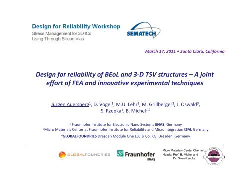
Design for reliability of BEoL and 3-D TSV structures – A ... - Sematech
Design for reliability of BEoL and 3-D TSV structures – A ... - Sematech
Design for reliability of BEoL and 3-D TSV structures – A ... - Sematech

Create successful ePaper yourself
Turn your PDF publications into a flip-book with our unique Google optimized e-Paper software.
March 17, 2011 • Santa Clara, Cali<strong>for</strong>nia<br />
<strong>Design</strong> <strong>for</strong> <strong>reliability</strong> <strong>of</strong> <strong>BEoL</strong> <strong>and</strong> 3‐D <strong>TSV</strong> <strong>structures</strong> <strong>–</strong>A joint<br />
ef<strong>for</strong>t <strong>of</strong> FEA <strong>and</strong> innovative experimental techniques<br />
Jürgen Auersperg 1 , D. Vogel 1 , M.U. Lehr 3 , M. Grillberger 3 , J. Oswald 3 ,<br />
S. Rzepka 1 , B. Michel 1,2<br />
1<br />
Fraunh<strong>of</strong>er Institute <strong>for</strong> Electronic Nano Systems ENAS, Germany<br />
2<br />
Micro Materials Center at Fraunh<strong>of</strong>er Institute <strong>for</strong> Reliability bl <strong>and</strong> Microintegration IZM, Germany<br />
4<br />
GLOBALFOUNDRIES Dresden Module One LLC & Co. KG, Dresden, Germany<br />
Micro Materials Center Chemnitz<br />
Heads: Pr<strong>of</strong>. B. Michel <strong>and</strong><br />
Dr. Sven Rzepka
Outline<br />
• Motivation<br />
• Multi‐level FE modeling <strong>of</strong> CPI<br />
• Multi‐failure evaluation <strong>for</strong><br />
Near‐Chip‐Edge <strong>and</strong> Near‐Bump Cracks in <strong>BEoL</strong><br />
• Role <strong>of</strong> Initial Stresses<br />
• <strong>TSV</strong> <strong>–</strong>damage <strong>and</strong> delamination investigation<br />
• Required experiments<br />
• Summary <strong>and</strong> Outlook<br />
Jürgen Auersperg, D. Vogel, M.U. Lehr,<br />
M. Grillberger, J. Oswald, S. Rzepka, B. Michel<br />
Micro Materials Center Chemnitz<br />
Heads: Pr<strong>of</strong>. B. Michel <strong>and</strong><br />
Dr. Sven Rzepka
Task <strong>–</strong> Heterogeneous Integration ‐ Packaging<br />
Bridging the gap between chip <strong>and</strong> application<br />
Bump side<br />
Multiscale <strong>–</strong>why?<br />
Geometry<br />
Packaged microprocessor<br />
(eight symmetric model<br />
Packaged microprocessor<br />
(10 <strong>–</strong>40 mm size)<br />
<strong>BEoL</strong> stack region<br />
Ni layer<br />
PI layer<br />
Bump side<br />
HMT solder<br />
Underfill<br />
<strong>BEoL</strong>‐stack<br />
(5 <strong>–</strong>10 µm size)<br />
Feature sizes:<br />
some nm!<br />
Transistor side<br />
Multiscale <strong>–</strong>why?<br />
Geometry<br />
Bridge 40 mm to sub‐nm <strong>for</strong><br />
Chip Packaging Interaction investigations <strong>of</strong><br />
a <strong>BEoL</strong> structure<br />
Structural details: sub ‐ nm<br />
Jürgen Auersperg, D. Vogel, M.U. Lehr,<br />
M. Grillberger, J. Oswald, S. Rzepka, B. Michel<br />
Micro Materials Center Chemnitz<br />
Heads: Pr<strong>of</strong>. B. Michel <strong>and</strong><br />
Dr. Sven Rzepka
Multiscale <strong>–</strong>why?<br />
Structure<br />
Nano lawn <strong>for</strong><br />
interconnect<br />
<strong>for</strong>mation<br />
Can these materials longer be<br />
modeled as homogeneous<br />
materials?<br />
Atomistic level modeling<br />
Molecular dynamics<br />
Jürgen Auersperg, D. Vogel, M.U. Lehr,<br />
M. Grillberger, J. Oswald, S. Rzepka, B. Michel<br />
Low‐k dielectrics (nano‐porous)<br />
Polymer: 23 H2O <strong>for</strong> 98 °C/ 100 RH<br />
Micro Materials Center Chemnitz<br />
Heads: Pr<strong>of</strong>. B. Michel <strong>and</strong><br />
Dr. Sven Rzepka
Multiscale ‐ Molecular Dynamics <strong>–</strong>Two Ways used<br />
Structure<br />
The way I:<br />
1. Modeling <strong>of</strong> the molecular structure<br />
2. Homogenization in a unit cell<br />
3. Use it directly inside a Macro‐model,<br />
a FE‐Model <strong>for</strong> instance<br />
The way II:<br />
1. Modeling <strong>of</strong> the molecular structure<br />
2. Simulations towards extraction <strong>of</strong> key‐<br />
properties Finite (YOUNG’s Element modulus, Region CTE,<br />
diffusion coefficients)<br />
Crack Tip Molecular<br />
3. Use these properties Dynamics Region inside a Macrodla<br />
FE‐Model l<strong>for</strong> instance<br />
model, Jürgen Auersperg, D. Vogel, M.U. Lehr,<br />
M. Grillberger, J. Oswald, S. Rzepka, B. Michel<br />
Polymer: 23 H2O <strong>for</strong> 98 °C/ 100 RH<br />
Micro Materials Center Chemnitz<br />
Heads: Pr<strong>of</strong>. B. Michel <strong>and</strong><br />
Dr. Sven Rzepka
Moisture Diffusion in Epoxy by Molecular Dynamics<br />
Motivation:<br />
i<br />
Underst<strong>and</strong> diffusion phenomena as structureproperty<br />
correlation <strong>for</strong> <strong>reliability</strong> prediction<br />
Structure<br />
Method<br />
Materials: Epoxy with sev. chem. composition<br />
Exp: measure diffusion D & saturation S<br />
Sim: molecular dynamics<br />
Result:<br />
D <strong>and</strong> S are strong functions <strong>of</strong> (as tested)<br />
‐ density,<br />
‐ polarity,<br />
‐ chain length,<br />
‐ stoichiometry,<br />
‐ temperature<br />
Sim & Exp show correct tendencies<br />
Quantitative Results need correct<br />
3D network representation <strong>of</strong> epoxy resins<br />
Jürgen Auersperg, D. Vogel, M.U. Lehr,<br />
E.D. M. Dermitzaki, Grillberger, J. Bauer, J. Oswald, B. Wunderle, S. Rzepka, B. B. Michel Michel<br />
m^2/s) oeff.<br />
Diff D co (cm<br />
2.50E-007<br />
2.00E-007<br />
1.50E-007<br />
1.00E-007<br />
5.00E-008<br />
0.00E+00000E 000<br />
Polymer: 23 H2O <strong>for</strong> 98 °C/ 100 RH<br />
Varied parameters = Arrow:<br />
increasing polarity <strong>and</strong> chain lenght<br />
Exp<br />
Experiment:98°C/100RH<br />
Diff co oeff.<br />
2/s)<br />
D (cm^<br />
3.0x10 -6<br />
2.5x10 -6<br />
2.0x10 -6<br />
1.5x10 -6<br />
1.0x10 -6<br />
5.0x10 -7<br />
00 0.0<br />
98 °C/ 100 rh<br />
Micro Materials Center Chemnitz<br />
Heads: Pr<strong>of</strong>. B. Michel <strong>and</strong><br />
Dr. Sven Rzepka<br />
Sim<br />
Molecular Dynamics 98°C/100RH
Multiscale <strong>–</strong> Finite Element Techniques ‐ Substructuring<br />
Continuum<br />
Multi‐level<br />
Substructuring<br />
256x<br />
3<br />
4<br />
2<br />
1<br />
Jürgen Auersperg, D. Vogel, M.U. Lehr,<br />
M. Grillberger, J. Oswald, S. Rzepka, B. Michel<br />
Micro Materials Center Chemnitz<br />
Heads: Pr<strong>of</strong>. B. Michel <strong>and</strong><br />
Dr. Sven Rzepka
Multiscale <strong>–</strong> Finite Element Techniques <strong>–</strong> Submodeling<br />
Continuum<br />
Multi‐level<br />
Submodeling<br />
256x<br />
2<br />
1<br />
3<br />
4<br />
Jürgen Auersperg, D. Vogel, M.U. Lehr,<br />
M. Grillberger, J. Oswald, S. Rzepka, B. Michel<br />
Micro Materials Center Chemnitz<br />
Heads: Pr<strong>of</strong>. B. Michel <strong>and</strong><br />
Dr. Sven Rzepka
Multi‐failure Evaluation<br />
Micro Materials Center Chemnitz<br />
Heads: Pr<strong>of</strong>. B. Michel <strong>and</strong><br />
Dr. Sven Rzepka
2 nd Failure‐Mode <strong>–</strong> Risk <strong>for</strong> Die‐Cracking, Cracking <strong>of</strong> Substrates, …<br />
Smooth bending<br />
w/o singularities in<br />
Stress field with<br />
well known stress<br />
stresses/strains singularity 1 r<br />
Stress field with<br />
stress singularity<br />
1<br />
r<br />
Well known angle from<br />
anisotropic etching, <strong>for</strong> instance<br />
Classical l strength thhypotheses<br />
Generalized stress intensity<br />
it Fracture mechanics:<br />
max. surface stress evaluation factor (gSIF) A‐factor …<br />
K‐factor (SIF), J‐integral, energy<br />
Weibull‐plots<br />
release rate (ERR) …<br />
Jürgen Auersperg, D. Vogel, M.U. Lehr,<br />
M. Grillberger, J. Oswald, S. Rzepka, B. Michel<br />
Micro Materials Center Chemnitz<br />
Heads: Pr<strong>of</strong>. B. Michel <strong>and</strong><br />
Dr. Sven Rzepka
3 rd Failure‐Mode <strong>–</strong> Delamination at Materials Interfaces<br />
20µm<br />
<br />
( <br />
i<br />
) 0<br />
xx<br />
yy<br />
<br />
K r<br />
i<br />
/<br />
2<br />
r<br />
Hutchinson et al.<br />
1992<br />
r<br />
0<br />
<br />
<br />
2a<br />
exp <br />
2<br />
<br />
<br />
<strong>for</strong> <br />
yy<br />
<strong>and</strong><br />
r<br />
*<br />
0<br />
<br />
a<br />
<br />
2 exp <br />
<br />
<br />
<br />
<strong>for</strong> <br />
xy<br />
Mixed Mode Situation<br />
Jürgen Auersperg, D. Vogel, M.U. Lehr,<br />
M. Grillberger, J. Oswald, S. Rzepka, B. Michel<br />
Micro Materials Center Chemnitz<br />
Heads: Pr<strong>of</strong>. B. Michel <strong>and</strong><br />
Dr. Sven Rzepka
Cohesive Zone Modeling <strong>–</strong>Drawbacks <strong>and</strong> Challenges<br />
CZM<br />
DCB specimen with crack propagation under continuous<br />
displacement controlled opening<br />
! CZM‐Models have to h<strong>and</strong>le <strong>and</strong><br />
deliver damage parameters<br />
(damage progress per<br />
cycle/time)<br />
CZM with damage options<br />
Subjects <strong>of</strong> current research!<br />
Jürgen Auersperg, D. Vogel, M.U. Lehr,<br />
M. Grillberger, J. Oswald, S. Rzepka, B. Michel<br />
Micro Materials Center Chemnitz<br />
Heads: Pr<strong>of</strong>. B. Michel <strong>and</strong><br />
Dr. Sven Rzepka
XFEM ‐ Mesh Independent Crack Propagation<br />
XFEM<br />
FEM shape functions<br />
FEM unknowns<br />
Discontinuous<br />
enrichment functions<br />
XFEM unknowns<br />
FEM<br />
displacement<br />
all nodes<br />
Crack crossing an element<br />
XFEM<br />
Heaviside enrichment<br />
subset <strong>of</strong> nodes<br />
Crack tip in an element<br />
Jürgen Auersperg, D. Vogel, M.U. Lehr,<br />
M. Grillberger, J. Oswald, S. Rzepka, B. Michel<br />
Micro Materials Center Chemnitz<br />
Heads: Pr<strong>of</strong>. B. Michel <strong>and</strong><br />
Dr. Sven Rzepka
<strong>BEoL</strong> Stack <strong>of</strong> an IC <strong>–</strong> Cracking/Delamination ‐ Locations <strong>and</strong> Impacts<br />
Near-chip-edge cracks under Chip Package Interaction (CPI)<br />
Crack stop structure<br />
Near-bump cracking during reflow<br />
(NBC)<br />
Leadfree<br />
Copper Pillars<br />
Jürgen Auersperg, D. Vogel, M.U. Lehr,<br />
M. Grillberger, J. Oswald, S. Rzepka, B. Michel<br />
Micro Materials Center Chemnitz<br />
Heads: Pr<strong>of</strong>. B. Michel <strong>and</strong><br />
Dr. Sven Rzepka
Chip Package Interaction (CPI)<br />
Near-chip-edge cracks<br />
Micro Materials Center Chemnitz<br />
Heads: Pr<strong>of</strong>. B. Michel <strong>and</strong><br />
Dr. Sven Rzepka
<strong>BEoL</strong> Stack <strong>of</strong> an IC <strong>–</strong>Near‐Bump‐Cracks <strong>–</strong>Region <strong>of</strong> Interest<br />
NBC<br />
Packaged FE‐model<br />
(eight symmetric model)<br />
LID adhesive<br />
<strong>BEoL</strong> stack region<br />
Ni layer<br />
PI layer<br />
TIM1<br />
Die<br />
Underfill<br />
Soldermask<br />
HMT solder<br />
Underfill<br />
Board<br />
gap<br />
LJT solder<br />
Soldermask<br />
Boardpad<br />
Jürgen Auersperg, D. Vogel, M.U. Lehr,<br />
M. Grillberger, J. Oswald, S. Rzepka, B. Michel<br />
Micro Materials Center Chemnitz<br />
Heads: Pr<strong>of</strong>. B. Michel <strong>and</strong><br />
Dr. Sven Rzepka
3D <strong>BEoL</strong> Stack Part‐model <strong>–</strong> Submodeling with Sub<strong>structures</strong><br />
NBC<br />
Substructure<br />
Finite elelement<br />
characteristic size in<br />
<strong>BEoL</strong>‐stack<br />
< nm<br />
Substructure region<br />
Replacement <strong>of</strong> the finest (1x) <strong>structures</strong><br />
by superelements (repeatedly used) leads<br />
to a dramatically reduced model size<br />
(by factor 3),<br />
complete model<br />
(with <strong>and</strong> without element edges)<br />
vias <strong>and</strong><br />
metal traces<br />
Jürgen Auersperg, D. Vogel, M.U. Lehr,<br />
M. Grillberger, J. Oswald, S. Rzepka, B. Michel<br />
Micro Materials Center Chemnitz<br />
Heads: Pr<strong>of</strong>. B. Michel <strong>and</strong><br />
Dr. Sven Rzepka
3d Local Model <strong>of</strong> a <strong>BEoL</strong> Part <strong>–</strong>Crack Introduced ‐ SubModeling<br />
NBC<br />
Global model<br />
Submodel<br />
Initial crack<br />
Jürgen Auersperg, D. Vogel, M.U. Lehr,<br />
M. Grillberger, J. Oswald, S. Rzepka, B. Michel<br />
Micro Materials Center Chemnitz<br />
Heads: Pr<strong>of</strong>. B. Michel <strong>and</strong><br />
Dr. Sven Rzepka
3d Local Model <strong>of</strong> a <strong>BEoL</strong> Part <strong>–</strong> SubModel Placing <strong>and</strong> Orientation<br />
NBC<br />
Submodel driving nodes<br />
Jürgen Auersperg, D. Vogel, M.U. Lehr,<br />
M. Grillberger, J. Oswald, S. Rzepka, B. Michel<br />
Micro Materials Center Chemnitz<br />
Heads: Pr<strong>of</strong>. B. Michel <strong>and</strong><br />
Dr. Sven Rzepka
Multiscale <strong>–</strong>Substructure & Submodeling <strong>of</strong> a <strong>BEoL</strong> stack <strong>of</strong> an IC<br />
NBC<br />
Mode II<br />
(In‐Plane Shear)<br />
Mode III<br />
(Out‐<strong>of</strong>‐Plane Shear)<br />
Jürgen Auersperg, D. Vogel, M.U. Lehr,<br />
M. Grillberger, J. Oswald, S. Rzepka, B. Michel<br />
Micro Materials Center Chemnitz<br />
Heads: Pr<strong>of</strong>. B. Michel <strong>and</strong><br />
Dr. Sven Rzepka
Multiscale <strong>–</strong>Substructure & Submodeling <strong>of</strong> a <strong>BEoL</strong> stack <strong>of</strong> an IC<br />
NBC<br />
Crack kdii driving <strong>for</strong>ce along the crack front<br />
Results:<br />
• Find most critical places with<br />
• Material interface delamination<br />
<strong>and</strong>/or<br />
• Cohesive fracture <strong>of</strong> material<br />
Jürgen Auersperg, D. Vogel, M.U. Lehr,<br />
M. Grillberger, J. Oswald, S. Rzepka, B. Michel<br />
Micro Materials Center Chemnitz<br />
Heads: Pr<strong>of</strong>. B. Michel <strong>and</strong><br />
Dr. Sven Rzepka
<strong>BEoL</strong> Stack <strong>of</strong> an IC <strong>–</strong>Die Edge Cracking ‐ Interface Fracture Mechanics<br />
CPI<br />
1,40<br />
max. norm. ERR vs Crack Length<br />
orm. G<br />
n<br />
1,20<br />
1,00<br />
0,80<br />
060<br />
0,60<br />
Chip corner<br />
0,40<br />
margin 51 µm to crack-stop-structure<br />
0,20<br />
0,00<br />
margin 51 µm to crack-stop-structure<br />
w/o crack-stop-structure<br />
structure<br />
0 20 40 60 80 100 120<br />
crack length [µm]<br />
Crack stop structure<br />
t<br />
Margin<br />
Jürgen Auersperg, D. Vogel, M.U. Lehr,<br />
M. Grillberger, J. Oswald, S. Rzepka, B. Michel<br />
Micro Materials Center Chemnitz<br />
Heads: Pr<strong>of</strong>. B. Michel <strong>and</strong><br />
Dr. Sven Rzepka
<strong>BEoL</strong> Stack <strong>of</strong> an IC <strong>–</strong>Die Edge Cracking ‐ Interface Fracture Mechanics<br />
CPI<br />
• 10 bimaterial interface paths +<br />
• 4 cohesive crack paths in ULK<br />
3<br />
Max. ERR in diff. Crack Paths, 40 µm Crack Length marg 100<br />
2,9<br />
2,8<br />
ge<br />
en. G<br />
2,7<br />
2,6<br />
Chip corner<br />
2,5<br />
Path<br />
24<br />
2,4<br />
Crack stop structure<br />
t<br />
2,3<br />
1 2 3 4 5 6 7 8 9 path<br />
10<br />
Margin<br />
Jürgen Auersperg, D. Vogel, M.U. Lehr,<br />
M. Grillberger, J. Oswald, S. Rzepka, B. Michel<br />
Micro Materials Center Chemnitz<br />
Heads: Pr<strong>of</strong>. B. Michel <strong>and</strong><br />
Dr. Sven Rzepka
NBC<br />
Reflow Process Dependent<br />
Near‐Bump‐Cracks in <strong>BEoL</strong><br />
Leadfree<br />
Micro Materials Center Chemnitz<br />
Heads: Pr<strong>of</strong>. B. Michel <strong>and</strong><br />
Dr. Sven Rzepka
3d Global‐Local Model Simulations <strong>–</strong>Stress States<br />
NBC<br />
Peeling Stresses at 0 °C (under CPI)<br />
Peeling Stresses at RT (end <strong>of</strong> reflow)<br />
Chip center<br />
Chip center<br />
Chip center<br />
Avoid worst case: white spots in SAM<br />
Jürgen Auersperg, D. Vogel, M.U. Lehr,<br />
M. Grillberger, J. Oswald, S. Rzepka, B. Michel<br />
Micro Materials Center Chemnitz<br />
Heads: Pr<strong>of</strong>. B. Michel <strong>and</strong><br />
Dr. Sven Rzepka
Cooling Down from Soldering <strong>–</strong>Reflow Pr<strong>of</strong>iles<br />
NBC<br />
Highlead<br />
Leadfree<br />
Aggressive cooling<br />
slope<br />
Some studies have shown<br />
that an aggressive cooling<br />
slope can provide optimal<br />
diffusion <strong>of</strong> material <strong>and</strong><br />
fine eutectic grain<br />
<strong>structures</strong><br />
Mohanty, R., Apell, M. C., Burke,<br />
R.: Reflow Process Control<br />
Monitoring, <strong>and</strong> Data Logging,<br />
URL:<br />
http://www.emsnow.com/cnt/fil<br />
es/White%20Papers/speedReflo<br />
wProcessControl.pdf<br />
Jürgen Auersperg, D. Vogel, M.U. Lehr,<br />
M. Grillberger, J. Oswald, S. Rzepka, B. Michel<br />
Micro Materials Center Chemnitz<br />
Heads: Pr<strong>of</strong>. B. Michel <strong>and</strong><br />
Dr. Sven Rzepka
FE‐Modeling <strong>of</strong> the Soldering Process <strong>–</strong>Reflow Pr<strong>of</strong>ile Modification<br />
NBC<br />
• Highest G <strong>for</strong> Leadfree Soldering<br />
• Stress relaxation <strong>of</strong> the solder joints<br />
Temperature vs. Time<br />
300<br />
Leadfree pr<strong>of</strong>ile<br />
250<br />
Leadfree pr<strong>of</strong>ile 02<br />
Highlead pr<strong>of</strong>ile<br />
200 Highled pr<strong>of</strong>ile 02<br />
Highled pr<strong>of</strong>ile 03<br />
150<br />
100<br />
50<br />
0<br />
0 400 800 1200 1600 2000<br />
Cooling down<br />
period discussed<br />
here<br />
Jürgen Auersperg, D. Vogel, M.U. Lehr,<br />
M. Grillberger, J. Oswald, S. Rzepka, B. Michel<br />
Micro Materials Center Chemnitz<br />
Heads: Pr<strong>of</strong>. B. Michel <strong>and</strong><br />
Dr. Sven Rzepka
Crack <strong>and</strong> Damage Initiation/Propagation Investigation<br />
NBC<br />
Damage<br />
Problems:<br />
Material/Interface properties<br />
Integration Stability/Controlability<br />
Damage propagation investigation in order<br />
to find highest damage risk locations<br />
XFEM<br />
XFEM in order to find crack starting locations<br />
<strong>and</strong> paths<br />
Jürgen Auersperg, D. Vogel, M.U. Lehr,<br />
M. Grillberger, J. Oswald, S. Rzepka, B. Michel<br />
Micro Materials Center Chemnitz<br />
Heads: Pr<strong>of</strong>. B. Michel <strong>and</strong><br />
Dr. Sven Rzepka
Chip Package Interaction <strong>and</strong> Initial Stresses<br />
From Manufacturing Processes<br />
Micro Materials Center Chemnitz<br />
Heads: Pr<strong>of</strong>. B. Michel <strong>and</strong><br />
Dr. Sven Rzepka
Local Residual Stress Measurement ‐ Approaches ‐<br />
Electron Back Scattered Diffraction<br />
(EBSD) based method<br />
• de<strong>for</strong>mation <strong>of</strong> Kikuchi diffraction pattern<br />
as measure <strong>of</strong> stress<br />
• determines stress tensor comp.<br />
Residual<br />
Stresses<br />
Stress Release Technique (fibDAC)<br />
utilizing de<strong>for</strong>mation field after trench<br />
milling by FIB<br />
Raman Spectroscopy<br />
• uses shift <strong>of</strong> Raman<br />
b<strong>and</strong>s due to stress<br />
• TERS effect with<br />
potential to obtain<br />
resolution beyond 100<br />
nm<br />
D. Jürgen Vogel, A. Auersperg, Gollhardt<br />
D. Vogel, M.U. Lehr,<br />
M. Grillberger, J. Oswald, S. Rzepka, B. Michel<br />
Micro Materials Center Chemnitz<br />
Heads: Pr<strong>of</strong>. B. Michel <strong>and</strong><br />
Dr. Sven Rzepka
Local stress measurement concept <strong>–</strong>stress relief by FIB milling (fibDAC)<br />
Material removal<br />
by<br />
FIB feature milling<br />
Stress relief, i.e.<br />
de<strong>for</strong>mation<br />
nearby milling pattern<br />
Solution <strong>of</strong> the<br />
Quantifying<br />
mechanical stress relief<br />
Displacement<br />
df de<strong>for</strong>mation field problem by<br />
field fitting<br />
by<br />
Digital Image<br />
Finite Element Analysis<br />
Correlation (DIC)<br />
(FEA)<br />
Stress values<br />
D. Jürgen Vogel, A. Auersperg, Gollhardt<br />
D. Vogel, M.U. Lehr,<br />
M. Grillberger, J. Oswald, S. Rzepka, B. Michel<br />
Micro Materials Center Chemnitz<br />
Heads: Pr<strong>of</strong>. B. Michel <strong>and</strong><br />
Dr. Sven Rzepka
Near‐Bump Cracks in <strong>BEoL</strong> <strong>–</strong> Taking Initial Stresses into Account<br />
Crack Paths 6 <strong>and</strong> 14 with ULK vs. Gen3<br />
During whole processing w/o <strong>and</strong><br />
with initial stresses<br />
1,2<br />
1<br />
max. ERR <strong>for</strong> all Steps at the Crack Front<br />
With initial stresses<br />
1,00000<br />
G<br />
0,8<br />
0,66285<br />
gen.<br />
0,6<br />
0,44671 0,43292<br />
0,4<br />
0,2<br />
0,22349<br />
0,12081<br />
0,18113<br />
0,10560<br />
0<br />
Path 6<br />
Path 6<br />
Path 14<br />
Path 14<br />
Path 6<br />
Path 6<br />
Path 14<br />
Path 14<br />
ULK Gen3 ULK Gen3 ULK is Gen3 is ULK is Gen3 is<br />
Jürgen Auersperg, D. Vogel, M.U. Lehr,<br />
M. Grillberger, J. Oswald, S. Rzepka, B. Michel<br />
Micro Materials Center Chemnitz<br />
Heads: Pr<strong>of</strong>. B. Michel <strong>and</strong><br />
Dr. Sven Rzepka
3D‐Integration ti <strong>–</strong> <strong>TSV</strong> <strong>and</strong> <strong>BEoL</strong><br />
Cracking/Delamination risks during <strong>BEoL</strong>‐manufacturing on top <strong>of</strong> <strong>TSV</strong>s?<br />
Micro Materials Center Chemnitz<br />
Heads: Pr<strong>of</strong>. B. Michel <strong>and</strong><br />
Dr. Sven Rzepka
<strong>TSV</strong> <strong>and</strong> <strong>BEoL</strong>‐structure<br />
Protrusion<br />
Jürgen Auersperg, D. Vogel, M.U. Lehr,<br />
M. Grillberger, J. Oswald, S. Rzepka, B. Michel<br />
Micro Materials Center Chemnitz<br />
Heads: Pr<strong>of</strong>. B. Michel <strong>and</strong><br />
Dr. Sven Rzepka
<strong>TSV</strong> <strong>and</strong> <strong>BEoL</strong>‐structure ‐ Possible Failure Mode <strong>–</strong> Delamination<br />
Protrusion<br />
Assumtions:<br />
• Initial delamination between <strong>TSV</strong> <strong>and</strong> barrier<br />
• Initial stresses in <strong>TSV</strong> <strong>and</strong> introduced step by step<br />
during <strong>BEoL</strong>‐processing<br />
• Partly delaminated <strong>BEoL</strong><br />
• Cracks in <strong>BEoL</strong><br />
Jürgen Auersperg, D. Vogel, M.U. Lehr,<br />
M. Grillberger, J. Oswald, S. Rzepka, B. Michel<br />
Micro Materials Center Chemnitz<br />
Heads: Pr<strong>of</strong>. B. Michel <strong>and</strong><br />
Dr. Sven Rzepka
<strong>TSV</strong> <strong>and</strong> <strong>BEoL</strong>‐structure <strong>–</strong> Delamination Investigation<br />
Changing stress<br />
traction direction<br />
Strong dependence on<br />
stress free assumptions<br />
Crack flanks partly in<br />
contact <strong>–</strong> negative Jint<br />
Jürgen Auersperg, D. Vogel, M.U. Lehr,<br />
M. Grillberger, J. Oswald, S. Rzepka, B. Michel<br />
Micro Materials Center Chemnitz<br />
Heads: Pr<strong>of</strong>. B. Michel <strong>and</strong><br />
Dr. Sven Rzepka
Sequential Build Up <strong>–</strong>Cohesive Zone Modeling <strong>–</strong> <strong>BEoL</strong> to MOL Delamination<br />
Cohesive zone elements introduced between MOL <strong>and</strong> <strong>BEoL</strong> <strong>–</strong> damaging during<br />
thermal loading delamination <strong>of</strong> initially undamaged material interface<br />
d<br />
Measure <strong>for</strong> interface<br />
loading (<strong>BEoL</strong> removed <strong>for</strong><br />
better demonstration<br />
Interface totally damaged at<br />
distance ‘d’<br />
<strong>TSV</strong><br />
Jürgen Auersperg, D. Vogel, M.U. Lehr,<br />
M. Grillberger, J. Oswald, S. Rzepka, B. Michel<br />
Silicon<br />
‣ Define CZM‐properties:<br />
Tn, Ts, Tt, GI, GII, GIII, En,<br />
Es, Et (all are estimated<br />
here!)<br />
Micro Materials Center Chemnitz<br />
Heads: Pr<strong>of</strong>. B. Michel <strong>and</strong><br />
Dr. Sven Rzepka
<strong>and</strong> <strong>BEoL</strong>‐structure ‐ Possible Failure Mode <strong>–</strong> Damaging <strong>of</strong> Copper<br />
‣ Define damage ‐<br />
properties:<br />
pl , ‐p/q, rate , G c , …)all<br />
are estimated here!)<br />
Jürgen Auersperg, D. Vogel, M.U. Lehr,<br />
M. Grillberger, J. Oswald, S. Rzepka, B. Michel<br />
Micro Materials Center Chemnitz<br />
Heads: Pr<strong>of</strong>. B. Michel <strong>and</strong><br />
Dr. Sven Rzepka
Material lProperty Dt Determination<br />
ti<br />
Size Dependent Material Behavior<br />
Micro Materials Center Chemnitz<br />
Heads: Pr<strong>of</strong>. B. Michel <strong>and</strong><br />
Dr. Sven Rzepka
Material Behavior ‐ Measure Required Properties<br />
Dynamical‐Mechanical Analysis (DMA) Thermomechanical Analysis (TMA) Creep data eval. (Solder)<br />
Temp.dep. creep data (Epoxy) Stress relaxation data (Epoxy) Poisson’s s ratio eval.<br />
Jürgen Auersperg, D. Vogel, M.U. Lehr,<br />
H. Walter, M. Grillberger, J. Auersperg J. Oswald, S. Rzepka, B. Michel<br />
Micro Materials Center Chemnitz<br />
Heads: Pr<strong>of</strong>. B. Michel <strong>and</strong><br />
Dr. Sven Rzepka
Nanoindentation in low‐K Dielectrics<br />
Bump side<br />
Thin layers<br />
<strong>BEoL</strong> stack<br />
7 µm<br />
F, u<br />
Intenter<br />
Thin Layer<br />
Substrate<br />
t<br />
For <strong>TSV</strong>:<br />
• Initial yield stress<br />
• Hardening ade gbehavior<br />
N]<br />
Force [µ<br />
1400<br />
1200<br />
1000<br />
800<br />
600<br />
400<br />
200<br />
Chip side<br />
Sim<br />
Measurement<br />
Experiment<br />
E=145, sy=1600-10000<br />
0<br />
0 20 40 60 80<br />
-200<br />
Distance [nm]<br />
Experiment Simulation Agreement<br />
Parameter <strong>–</strong> extraction only possible by coupled Sim & Exp<br />
Raul Jürgen<br />
Mrosko, Auersperg,<br />
Saskia Huber, D. Vogel,<br />
O. Wittler<br />
M.U. Lehr,<br />
M. Grillberger, J. Oswald, S. Rzepka, B. Michel<br />
Micro Materials Center Chemnitz<br />
Heads: Pr<strong>of</strong>. B. Michel <strong>and</strong><br />
Dr. Sven Rzepka
<strong>TSV</strong> Copper <strong>–</strong>YOUNGs Modulus by nano‐Indentation<br />
P13 Messung 3<br />
P13 Messung 3<br />
46,405<br />
demo demo demo demo demo<br />
<br />
<br />
<br />
140<br />
120<br />
<br />
<br />
<br />
<br />
Y(mm)<br />
46,400<br />
demo demo demo demo demo<br />
<br />
demo demo demo demo demo<br />
<br />
demo demo demo demo demo<br />
<br />
Er(GPa)<br />
100<br />
80<br />
60<br />
<br />
<br />
<br />
<br />
<br />
<br />
<br />
46,395<br />
<br />
demo demo demo demo demo<br />
40<br />
-82,275 275 -82,270 270 -82,265 265 -82,260<br />
260<br />
X(mm)<br />
demo demo demo demo demo<br />
<br />
46,390<br />
-82,275 -82,270 -82,265 -82,260<br />
X(mm)<br />
Jürgen Auersperg, D. Vogel, M.U. Lehr,<br />
M. Grillberger, J. Oswald, S. Rzepka, B. Michel<br />
Micro Materials Center Chemnitz<br />
Heads: Pr<strong>of</strong>. B. Michel <strong>and</strong><br />
Dr. Sven Rzepka
Copper Material Behavior<strong>–</strong> Properties Necessary<br />
Necessary to know:<br />
• Young's‐modulus dep. On Temperature<br />
• Initial yield stress<br />
• Hardening vs. plastic strains<br />
• Regarding <strong>TSV</strong>: initial stress state<br />
Xi Liu, Qiao Chen, Pradeep Dixit, Ritwik Chatterjee, Rao R.<br />
Tummala, <strong>and</strong> Suresh K. Sitaraman, Failure Mechanisms <strong>and</strong><br />
Optimum <strong>Design</strong> <strong>for</strong> Electroplated Copper Through‐Silicon Vias<br />
(<strong>TSV</strong>), 2009 Electronic Components <strong>and</strong> Technology<br />
Conference, pp. 624 ‐ 629<br />
Jürgen Auersperg, D. Vogel, M.U. Lehr,<br />
M. Grillberger, J. Oswald, S. Rzepka, B. Michel<br />
Micro Materials Center Chemnitz<br />
Heads: Pr<strong>of</strong>. B. Michel <strong>and</strong><br />
Dr. Sven Rzepka
Size Effects <strong>and</strong> Damage in Thin Metallic Films during Nano‐Indentation<br />
Meso‐mechanics <br />
Homogeneous<br />
• Strain gradient plasticity<br />
• Higher order stress theories<br />
Dislocation movement<br />
restrictions inside boundaries<br />
D. Gross, A. Trondl:<br />
Numerical Simulation <strong>of</strong> Size Effects <strong>and</strong><br />
Damage in Thin Metallic Films during Nano‐<br />
Indentation,<br />
Proc. ICF 12, Ottawa, CA, 2009, Paper on CD:<br />
fin00457.pdf<br />
Jürgen Auersperg, D. Vogel, M.U. Lehr,<br />
M. Grillberger, J. Oswald, S. Rzepka, B. Michel<br />
Micro Materials Center Chemnitz<br />
Heads: Pr<strong>of</strong>. B. Michel <strong>and</strong><br />
Dr. Sven Rzepka
Damage <strong>and</strong> Fracture Toughness Characterization<br />
ti<br />
Size Dependent Material Behavior<br />
Micro Materials Center Chemnitz<br />
Heads: Pr<strong>of</strong>. B. Michel <strong>and</strong><br />
Dr. Sven Rzepka
Interface Fracture Toughness Tests<br />
P<br />
Pull‐<strong>of</strong>f test schematic <strong>of</strong> substrate,<br />
interface <strong>and</strong> pull stud<br />
Modified CT‐specimen<br />
Peel test<br />
Pull‐out test Brazilian disk specimen Superlayer adhesion test<br />
A.A. Volinsky et al. / Acta Materialia 50 (2002) 441<strong>–</strong>466<br />
Jürgen Auersperg, D. Vogel, M.U. Lehr,<br />
M. Grillberger, J. Oswald, S. Rzepka, B. Michel<br />
Micro Materials Center Chemnitz<br />
Heads: Pr<strong>of</strong>. B. Michel <strong>and</strong><br />
Dr. Sven Rzepka
Interface Fracture Toughness Tests ‐ Bending<br />
Asymmetric Double Cantilever Beam<br />
Brazil‐Nut‐S<strong>and</strong>wich<br />
Single Leg Bending<br />
Symmetric Double Cantilever Beam<br />
4‐point bending<br />
Asymmetric DCB<br />
Asymmetric End‐Notched Flexure<br />
End‐Notched Flexure<br />
Sundaraman, Sitaraman 1997<br />
Center Cracked Beam<br />
Yeung, Lam, Yuen 2000<br />
Double Cantilever Beam<br />
Miller, Ho 2000<br />
Jürgen Auersperg, D. Vogel, M.U. Lehr,<br />
M. Grillberger, J. Oswald, S. Rzepka, B. Michel<br />
Micro Materials Center Chemnitz<br />
Heads: Pr<strong>of</strong>. B. Michel <strong>and</strong><br />
Dr. Sven Rzepka
Mode Separation/Evaluation <strong>–</strong>Critical ERR <strong>and</strong> Phase Angle<br />
Measured<br />
fracture<br />
toughness<br />
failure<br />
region<br />
Calculated<br />
crack<br />
loading<br />
Jürgen Auersperg, D. Vogel, M.U. Lehr,<br />
M. Grillberger, J. Oswald, S. Rzepka, B. Michel<br />
Micro Materials Center Chemnitz<br />
Heads: Pr<strong>of</strong>. B. Michel <strong>and</strong><br />
Dr. Sven Rzepka
Mode Separation/Evaluation <strong>–</strong>Critical ERR <strong>and</strong> Phase Angle<br />
<br />
<br />
<br />
1<br />
<br />
1<br />
G c<br />
G<br />
IC<br />
sin<br />
2<br />
<br />
<br />
With (a further material/interface parameter) is<br />
a function <strong>of</strong> temperature <strong>and</strong> moisture<br />
concentration<br />
G c<br />
failure<br />
region<br />
G() initiationi i i<br />
G()<br />
no initiation<br />
<br />
Hutchinson <strong>and</strong> Suo, "Mixed Mode Cracking in Layered<br />
Materials", Advances in Applied Mechanics, Vol. 29, pp.<br />
63-191<br />
Jürgen Auersperg, D. Vogel, M.U. Lehr,<br />
M. Grillberger, J. Oswald, S. Rzepka, B. Michel<br />
K. Liechti, Adhesion Measurements Relative to Electronic<br />
Packaging, Proc. 4th Annual Topical Conference On<br />
Reliability, October 30 - November 1, 2000<br />
Micro Materials Center Chemnitz<br />
Heads: Pr<strong>of</strong>. B. Michel <strong>and</strong><br />
Dr. Sven Rzepka
Nano‐Indentation <strong>for</strong> Interface Fracture Toughness Evaluation<br />
• Nanoindentation <strong>for</strong> “measuring“ Young’s<br />
modulus <strong>and</strong> hardness<br />
• Nanoindentation <strong>for</strong> “measuring“ fracture<br />
toughness<br />
Buckling<br />
• Nanoindentation <strong>for</strong> “measuring“ interfacial<br />
fracture toughness (adhesion) <strong>–</strong> Conical <strong>and</strong><br />
wedge indenters<br />
For instance:<br />
E.E. Gdoutos, A. Volinsky, Interfacial Fracture Toughness <strong>of</strong> Thin Films, Tutorial AC‐Conf., June 6, 2005<br />
M. R. Begley, D. R. Mumm, A. G. Evan, J. W. Hutchinson, Analysis <strong>of</strong> a Wedge Impression Test <strong>for</strong> Measuring the Interface<br />
Toughness Between Films/Coatings <strong>and</strong> Ductile Substrates, Acta mater. 48 (2000) 3211‐3220<br />
Jürgen Auersperg, D. Vogel, M.U. Lehr,<br />
M. Grillberger, J. Oswald, S. Rzepka, B. Michel<br />
Micro Materials Center Chemnitz<br />
Heads: Pr<strong>of</strong>. B. Michel <strong>and</strong><br />
Dr. Sven Rzepka
Stress State t Determination/Verification<br />
ti ifi ti<br />
Fitting modeling assumption with experimental results<br />
Micro Materials Center Chemnitz<br />
Heads: Pr<strong>of</strong>. B. Michel <strong>and</strong><br />
Dr. Sven Rzepka
<strong>TSV</strong> ‐ Stresses near the Surface <strong>–</strong>vs. Raman‐Spectroscopy<br />
zz<br />
rz<br />
<br />
rr<br />
M. Hecker, GlobalFoundries, Dresden<br />
Jürgen Auersperg, D. Vogel, M.U. Lehr,<br />
M. Grillberger, J. Oswald, S. Rzepka, B. Michel<br />
Micro Materials Center Chemnitz<br />
Heads: Pr<strong>of</strong>. B. Michel <strong>and</strong><br />
Dr. Sven Rzepka
Surface vs. Midd‐Stress rr<br />
Surface - rr<br />
Middle - <br />
Middle - rr<br />
Jürgen Auersperg, D. Vogel, M.U. Lehr,<br />
M. Grillberger, J. Oswald, S. Rzepka, B. Michel<br />
Micro Materials Center Chemnitz<br />
Heads: Pr<strong>of</strong>. B. Michel <strong>and</strong><br />
Dr. Sven Rzepka
Summary<br />
Multilevel lFE‐modelling <strong>of</strong> cracks in <strong>BEoL</strong>‐Struktures<br />
For Chip Package Interaction <strong>and</strong><br />
Reflow ‐ leadfree bumping<br />
Goal: Reliability enhancement<br />
Utilizing fracture mechanics concepts (cohesive <strong>and</strong> adhesive) <strong>and</strong>/or<br />
Damage mechanics approaches<br />
Jürgen Auersperg, D. Vogel, M.U. Lehr,<br />
M. Grillberger, J. Oswald, S. Rzepka, B. Michel<br />
Micro Materials Center Chemnitz<br />
Heads: Pr<strong>of</strong>. B. Michel <strong>and</strong><br />
Dr. Sven Rzepka
What we need<br />
Intensive experimental work necessary <strong>for</strong><br />
Evaluation <strong>of</strong> residual stresses from manufacturing,<br />
Evaluation <strong>of</strong> the material behavior (constitutive, size dependent)<br />
Characterization <strong>of</strong> the damage behavior <strong>of</strong> materials<br />
Characterization <strong>of</strong> strength/toughness properties (fracture mechanics<br />
characterization) <strong>of</strong> materials <strong>and</strong> materials interfaces<br />
Verification <strong>of</strong> simulation results<br />
Extensive simulation work necessary<br />
Huge simulation models <strong>and</strong> computing resources<br />
Theoretical work <strong>–</strong> delamination und fracture (CZM, XFEM), materials<br />
behavior (SGPM)<br />
Jürgen Auersperg, D. Vogel, M.U. Lehr,<br />
M. Grillberger, J. Oswald, S. Rzepka, B. Michel<br />
Micro Materials Center Chemnitz<br />
Heads: Pr<strong>of</strong>. B. Michel <strong>and</strong><br />
Dr. Sven Rzepka
What we Need <strong>for</strong> Helpful Simulation Results<br />
Residual stress<br />
characterization<br />
Damage <strong>and</strong> fracture<br />
characterization<br />
Material behavior <strong>and</strong> property<br />
characterization<br />
Simulation results<br />
verification<br />
Jürgen Auersperg, D. Vogel, M.U. Lehr,<br />
M. Grillberger, J. Oswald, S. Rzepka, B. Michel<br />
Micro Materials Center Chemnitz<br />
Heads: Pr<strong>of</strong>. B. Michel <strong>and</strong><br />
Dr. Sven Rzepka
Thank You <strong>for</strong> Your Attention!<br />
ti Micro Materials Center Chemnitz<br />
Heads: Pr<strong>of</strong>. B. Michel <strong>and</strong><br />
Dr. Sven Rzepka