LPR Sensor Made by Using Ordered Porous Alumina (PDF ... - Fujifilm
LPR Sensor Made by Using Ordered Porous Alumina (PDF ... - Fujifilm LPR Sensor Made by Using Ordered Porous Alumina (PDF ... - Fujifilm
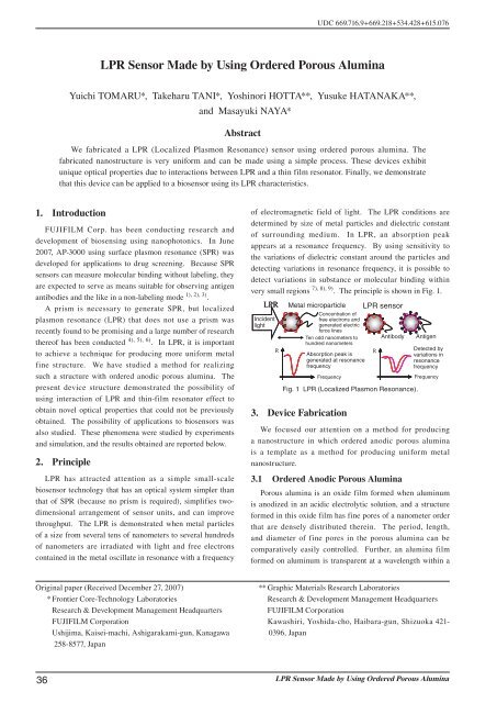
1. Original paper (Received December 27, 2007) * Frontier Core-Technology Laboratories Research & Development Management Headquarters FUJIFILM Corporation Ushijima, Kaisei-machi, Ashigarakami-gun, Kanagawa 258-8577, Japan 36 UDC 669.716.9+669.218+534.428+615.076 LPR Sensor Made by Using Ordered Porous Alumina Yuichi TOMARU*, Takeharu TANI*, Yoshinori HOTTA**, Yusuke HATANAKA**, and Masayuki NAYA* Abstract We fabricated a LPR (Localized Plasmon Resonance) sensor using ordered porous alumina. The fabricated nanostructure is very uniform and can be made using a simple process. These devices exhibit unique optical properties due to interactions between LPR and a thin film resonator. Finally, we demonstrate that this device can be applied to a biosensor using its LPR characteristics. Introduction FUJIFILM Corp. has been conducting research and development of biosensing using nanophotonics. In June 2007, AP-3000 using surface plasmon resonance (SPR) was developed for applications to drug screening. Because SPR sensors can measure molecular binding without labeling, they are expected to serve as means suitable for observing antigen antibodies and the like in a non-labeling mode 1), 2), 3) . A prism is necessary to generate SPR, but localized plasmon resonance (LPR) that does not use a prism was recently found to be promising and a large number of research thereof has been conducted 4), 5), 6) . In LPR, it is important to achieve a technique for producing more uniform metal fine structure. We have studied a method for realizing such a structure with ordered anodic porous alumina. The present device structure demonstrated the possibility of using interaction of LPR and thin-film resonator effect to obtain novel optical properties that could not be previously obtained. The possibility of applications to biosensors was also studied. These phenomena were studied by experiments and simulation, and the results obtained are reported below. 2. Principle LPR has attracted attention as a simple small-scale biosensor technology that has an optical system simpler than that of SPR (because no prism is required), simplifies twodimensional arrangement of sensor units, and can improve throughput. The LPR is demonstrated when metal particles of a size from several tens of nanometers to several hundreds of nanometers are irradiated with light and free electrons contained in the metal oscillate in resonance with a frequency of electromagnetic field of light. The LPR conditions are determined by size of metal particles and dielectric constant of surrounding medium. In LPR, an absorption peak appears at a resonance frequency. By using sensitivity to the variations of dielectric constant around the particles and detecting variations in resonance frequency, it is possible to detect variations in substance or molecular binding within very small regions 7), 8), 9) . The principle is shown in Fig. 1. Incident light 3. Metal microparticle Concentration of free electrons and generated electric force lines Ten odd nanometers to hundred nanometers Absorption peak is generated at resonance frequency Frequency LPR sensor Antibody Fig. 1 LPR (Localized Plasmon Resonance). Device Fabrication Antigen Detected by variations in resonance frequency Frequency We focused our attention on a method for producing a nanostructure in which ordered anodic porous alumina is a template as a method for producing uniform metal nanostructure. 3.1 Ordered Anodic Porous Alumina Porous alumina is an oxide film formed when aluminum is anodized in an acidic electrolytic solution, and a structure formed in this oxide film has fine pores of a nanometer order that are densely distributed therein. The period, length, and diameter of fine pores in the porous alumina can be comparatively easily controlled. Further, an alumina film formed on aluminum is transparent at a wavelength within a ** Graphic Materials Research Laboratories Research & Development Management Headquarters FUJIFILM Corporation Kawashiri, Yoshida-cho, Haibara-gun, Shizuoka 421- 0396, Japan LPR Sensor Made by Using Ordered Porous Alumina
- Page 2 and 3: ange of from visible light to infra
- Page 4 and 5: Fine pore depth 0.28 µm Fine pore
1.<br />
Original paper (Received December 27, 2007)<br />
* Frontier Core-Technology Laboratories<br />
Research & Development Management Headquarters<br />
FUJIFILM Corporation<br />
Ushijima, Kaisei-machi, Ashigarakami-gun, Kanagawa<br />
258-8577, Japan<br />
36<br />
UDC 669.716.9+669.218+534.428+615.076<br />
<strong>LPR</strong> <strong>Sensor</strong> <strong>Made</strong> <strong>by</strong> <strong>Using</strong> <strong>Ordered</strong> <strong>Porous</strong> <strong>Alumina</strong><br />
Yuichi TOMARU*, Takeharu TANI*, Yoshinori HOTTA**, Yusuke HATANAKA**,<br />
and Masayuki NAYA*<br />
Abstract<br />
We fabricated a <strong>LPR</strong> (Localized Plasmon Resonance) sensor using ordered porous alumina. The<br />
fabricated nanostructure is very uniform and can be made using a simple process. These devices exhibit<br />
unique optical properties due to interactions between <strong>LPR</strong> and a thin film resonator. Finally, we demonstrate<br />
that this device can be applied to a biosensor using its <strong>LPR</strong> characteristics.<br />
Introduction<br />
FUJIFILM Corp. has been conducting research and<br />
development of biosensing using nanophotonics. In June<br />
2007, AP-3000 using surface plasmon resonance (SPR) was<br />
developed for applications to drug screening. Because SPR<br />
sensors can measure molecular binding without labeling, they<br />
are expected to serve as means suitable for observing antigen<br />
antibodies and the like in a non-labeling mode 1), 2), 3) .<br />
A prism is necessary to generate SPR, but localized<br />
plasmon resonance (<strong>LPR</strong>) that does not use a prism was<br />
recently found to be promising and a large number of research<br />
thereof has been conducted 4), 5), 6) . In <strong>LPR</strong>, it is important<br />
to achieve a technique for producing more uniform metal<br />
fine structure. We have studied a method for realizing<br />
such a structure with ordered anodic porous alumina. The<br />
present device structure demonstrated the possibility of<br />
using interaction of <strong>LPR</strong> and thin-film resonator effect to<br />
obtain novel optical properties that could not be previously<br />
obtained. The possibility of applications to biosensors was<br />
also studied. These phenomena were studied <strong>by</strong> experiments<br />
and simulation, and the results obtained are reported below.<br />
2.<br />
Principle<br />
<strong>LPR</strong> has attracted attention as a simple small-scale<br />
biosensor technology that has an optical system simpler than<br />
that of SPR (because no prism is required), simplifies twodimensional<br />
arrangement of sensor units, and can improve<br />
throughput. The <strong>LPR</strong> is demonstrated when metal particles<br />
of a size from several tens of nanometers to several hundreds<br />
of nanometers are irradiated with light and free electrons<br />
contained in the metal oscillate in resonance with a frequency<br />
of electromagnetic field of light. The <strong>LPR</strong> conditions are<br />
determined <strong>by</strong> size of metal particles and dielectric constant<br />
of surrounding medium. In <strong>LPR</strong>, an absorption peak<br />
appears at a resonance frequency. By using sensitivity to<br />
the variations of dielectric constant around the particles and<br />
detecting variations in resonance frequency, it is possible to<br />
detect variations in substance or molecular binding within<br />
very small regions 7), 8), 9) . The principle is shown in Fig. 1.<br />
Incident<br />
light<br />
3.<br />
Metal microparticle<br />
Concentration of<br />
free electrons and<br />
generated electric<br />
force lines<br />
Ten odd nanometers to<br />
hundred nanometers<br />
Absorption peak is<br />
generated at resonance<br />
frequency<br />
Frequency<br />
<strong>LPR</strong> sensor<br />
Antibody<br />
Fig. 1 <strong>LPR</strong> (Localized Plasmon Resonance).<br />
Device Fabrication<br />
Antigen<br />
Detected <strong>by</strong><br />
variations in<br />
resonance<br />
frequency<br />
Frequency<br />
We focused our attention on a method for producing<br />
a nanostructure in which ordered anodic porous alumina<br />
is a template as a method for producing uniform metal<br />
nanostructure.<br />
3.1 <strong>Ordered</strong> Anodic <strong>Porous</strong> <strong>Alumina</strong><br />
<strong>Porous</strong> alumina is an oxide film formed when aluminum<br />
is anodized in an acidic electrolytic solution, and a structure<br />
formed in this oxide film has fine pores of a nanometer order<br />
that are densely distributed therein. The period, length,<br />
and diameter of fine pores in the porous alumina can be<br />
comparatively easily controlled. Further, an alumina film<br />
formed on aluminum is transparent at a wavelength within a<br />
** Graphic Materials Research Laboratories<br />
Research & Development Management Headquarters<br />
FUJIFILM Corporation<br />
Kawashiri, Yoshida-cho, Haibara-gun, Shizuoka 421-<br />
0396, Japan<br />
<strong>LPR</strong> <strong>Sensor</strong> <strong>Made</strong> <strong>by</strong> <strong>Using</strong> <strong>Ordered</strong> <strong>Porous</strong> <strong>Alumina</strong>
ange of from visible light to infrared radiation and can be<br />
easily used as an optical device.<br />
<strong>Ordered</strong> anodic porous alumina used as a template will be<br />
described below. Usually, when aluminum is anodized, fine<br />
pores are distributed randomly. However, where anodization<br />
is carried out under predetermined conditions after initiation<br />
points have been formed on the aluminum surface, the<br />
ordered pores are formed. The formation of initial initiation<br />
points can be performed <strong>by</strong> nanoimprinting or <strong>by</strong> using a<br />
form in which the initiation points are arranged in an ordered<br />
self-assembly in the bottom sections of fine pores during<br />
long-term anodization. The latter method is called a twostep<br />
anodization method, and because shape control <strong>by</strong> selfassembling<br />
makes it unnecessary to use a casting die such<br />
as a mold, the process cost can be reduced and the treated<br />
surface area can be increased. With consideration for utility,<br />
we selected the second method. Fig. 2 illustrates a schematic<br />
diagram of the two-step anodization method 10) .<br />
(1) Random pore<br />
formation<br />
(2) Ordering at<br />
bottom surface<br />
(3) <strong>Alumina</strong><br />
dissolution<br />
(4) Re-anodization<br />
Fig. 2 Processes of ordered porous alumina.<br />
The fine pore period P of the template depends on a<br />
voltage E of anodization and can be represented <strong>by</strong> equation<br />
P = 2.4 x E. The fine pore diameter is experimentally found<br />
to be about 1/3 cell period. The fine pore diameter can be<br />
enlarged <strong>by</strong> wet etching. The aluminum film thickness is<br />
determined <strong>by</strong> anodization time and a film with a maximum<br />
thickness of several hundreds of microns can be produced 11) .<br />
3.2 Device Fabrication<br />
The template used in the present report was subjected<br />
to first-step anodization for 5 hour under the following<br />
production conditions: 0.5M oxalic acid, voltage 40 V, liquid<br />
temperature 15˚C to obtain a fine pore period of 100 nm and<br />
then subjected to second-step anodization under the same<br />
conditions. The second-step anodization time was changed<br />
to obtain a film thickness of about 100 nm to 500 nm and a<br />
pore diameter of 30 nm to 90 nm according to the test object.<br />
Gold was vapor deposited on the film to a thickness of 30 nm.<br />
Fig. 3 shows a SEM observation image. Gold was formed as<br />
particles at the bottom of fine pores. A gold film was also<br />
formed on the alumina surface and a gold nanomesh structure<br />
was formed. A plurality of absorption peaks were confirmed<br />
to be present in the reflection spectrum of a visible range.<br />
We called the device obtained ADPAD (Anodic <strong>Porous</strong><br />
Aluminum device).<br />
FUJIFILM RESEARCH & DEVELOPMENT (No.53-2008)<br />
4.<br />
SEM images of ADPAD<br />
Top view<br />
Broken-out section<br />
Imaging view<br />
Inside of fine pore<br />
Fig. 3 ADPAD (Anodic <strong>Porous</strong> Aluminum Device).<br />
Reflection Optical Characteristic of<br />
ADPAD<br />
In order to study optical characteristics of the ADPAD, an<br />
optical evaluation system shown in Fig. 4 was prepared and<br />
a reflection spectrum was measured. The device was fixed<br />
with a cell-type holder so as to enable evaluation in liquid.<br />
The reflection spectrum was measured under illumination<br />
(incidence angle 10°) with a white parallel beam (xenon light<br />
source).<br />
Sample solution<br />
Window<br />
Optical fiber<br />
Polarizing plate<br />
<strong>LPR</strong> sensor device<br />
Fig. 4 Optical evaluation system.<br />
Polychromator<br />
Xenon lamp<br />
A plurality of absorption peaks can be seen in a reflection<br />
characteristic of the ADPAD, as shown in Fig. 5. The<br />
absorption peaks change depending on the alumina film<br />
thickness, and good match with the calculation results of<br />
simple thin-film interference cannot be obtained. Further,<br />
if this reflection characteristic is considered only as a <strong>LPR</strong><br />
characteristic, the fact that absorption peaks change even<br />
when the particle size or surrounding medium does not<br />
change contradicts the <strong>LPR</strong> characteristic. We built up a<br />
hypothesis according to which <strong>LPR</strong> and an optical resonator<br />
effect in a thin film are mixed together to cause such an<br />
optical characteristic. The principle of such a phenomenon is<br />
described below.<br />
Film thickness - 130 nm<br />
Film thickness = 230 nm<br />
Film thickness = 330 nm<br />
Fig. 5 Film thickness dependency of a spectrum.<br />
37
A simple model of ADPAD structure is shown in Fig. 6.<br />
The absorption peak generation principle is supposed to be<br />
based on a complex action of <strong>LPR</strong> absorption <strong>by</strong> gold particles<br />
formed at the bottom of fine pores and an interference effect<br />
created <strong>by</strong> a resonator formed <strong>by</strong> an aluminum base, a<br />
reflection layer of gold nanomesh at the outermost surface,<br />
and an intermediate transparent alumina layer. These<br />
hypotheses were examined <strong>by</strong> 3D-FDTD simulation and<br />
the aforementioned principle was studied. The results are<br />
presented below.<br />
Local plasmon<br />
resonance<br />
4.1<br />
38<br />
Resonator thin-film<br />
interference<br />
Fig. 6 Simple model of ADPAD.<br />
Local plasmon resonance +<br />
Resonator thin-film interference<br />
composite structure<br />
Study of Principle on the Basis of<br />
Hypothetical Models<br />
The principle was studied <strong>by</strong> computations performed with<br />
3D-FDTD. Fig. 7 shows the computation model and results<br />
obtained. The results obtained <strong>by</strong> computing the structure<br />
similar to that of the ADPAD with a model were used as a<br />
reference (blue line), and the reflection spectrum shape was<br />
compared for two hypothetical models: a model (red line) in<br />
which gold particles are present only in the fine pores and<br />
a model (yellow line) in which gold is present only on the<br />
surface. The depth of fine pores in the model structure is 200<br />
nm and the fine pore diameter is 50 nm.<br />
No Au on the surface<br />
No Au inside fine pores<br />
No Au on the surface<br />
No Au inside fine pores<br />
Electric field<br />
intensity distribution<br />
Local plasmon<br />
resonance,<br />
Au absorption<br />
inside fine pores<br />
Resonator thin-film<br />
interference,<br />
surface Au absorption<br />
Fig. 7 The calculation result of the spectrum origin.<br />
With the model shown in Fig. 7, it was found that<br />
the absorption on the long wavelength side originates in<br />
interference, whereas the absorption on the short wavelength<br />
side is the <strong>LPR</strong> absorption of gold particles. In addition,<br />
the portion within a round symbol in the graph indicates<br />
the generation of <strong>LPR</strong> absorption originating in the gold<br />
nanomesh structure. The computation results demonstrated<br />
that the spectrum included, as had been supposed, the <strong>LPR</strong><br />
absorption and the interference absorption.<br />
4.2 <strong>LPR</strong> and Resonator Effect<br />
Fig. 8 and Fig. 9 show computation results relating to<br />
reflection spectra obtained under variable alumina film<br />
thickness.<br />
With the fine pore thickness of 0.28 µm shown in Fig. 8,<br />
the <strong>LPR</strong> absorption (close to 800 nm) and the interference<br />
absorption were independent. When the fine pore depth was<br />
0.4 µm, the <strong>LPR</strong> absorption and the interference absorption<br />
coincided at a wavelength close to 800 nm. However, the<br />
spectrum was split in two, without overlapping. The two<br />
did not simply supplemented one another. In Fig. 9, of<br />
the results obtained <strong>by</strong> fine computations of film thickness<br />
conditions, the absorption wavelength obtained <strong>by</strong><br />
computation was plotted <strong>by</strong> blue points, the wavelength<br />
originating in interference absorption was plotted <strong>by</strong> a red<br />
line, and the <strong>LPR</strong> absorption wavelength was plotted <strong>by</strong> a<br />
blue line. When the interference absorption wavelength and<br />
<strong>LPR</strong> absorption wavelength were separate, the respective<br />
absorption wavelengths matched theoretical values, and the<br />
spectra separated when the two absorption wavelengths came<br />
close to one another.<br />
Fig. 10 shows the results obtained <strong>by</strong> measuring a<br />
reflection spectrum with an actual device in which film<br />
thickness conditions of ADPAD were finely changed and<br />
plotting the absorption wavelength in the same way as in Fig.<br />
9. The device film thickness was calculated from the SEM<br />
image, and although it included an error, the measurement<br />
results obtained with the actual device also demonstrated<br />
that the plots tend to separate in a wavelength region (close<br />
to 780 nm) where the <strong>LPR</strong> absorption and the interference<br />
absorption match. The blue line in the graph indicates a<br />
wavelength position where the <strong>LPR</strong> absorption is generated.<br />
As the fine pore diameter of the ADPAD decreases (in other<br />
words, the size of gold dot decreases, the wavelength at<br />
which the spectrum separation occurs shifts toward shorter<br />
wavelengths.<br />
Thus, the <strong>LPR</strong> effect and the resonator effect are not<br />
completely independent and demonstrate some kind of<br />
interaction. This is of great physical interest as a phenomenon<br />
indicating strong interaction of light (resonator) and electrons<br />
(plasmons) 12) .<br />
<strong>LPR</strong> <strong>Sensor</strong> <strong>Made</strong> <strong>by</strong> <strong>Using</strong> <strong>Ordered</strong> <strong>Porous</strong> <strong>Alumina</strong>
Fine pore depth 0.28 µm<br />
Fine pore depth 0.4 µm<br />
Fig. 8 The calculation result of the film thickness dependency of<br />
spectrum A.<br />
FDTD computed absorption wavelength plot<br />
Interference absorption wavelength<br />
Local plasmon absorption wavelength<br />
Fig. 9 The calculation result of the film thickness dependency of<br />
spectrum B.<br />
Film thickness (graph value)<br />
Wave length<br />
Fig. 10 The experiment result of<br />
the film thickness dependency of a spectrum.<br />
5.<br />
Performance of ADPAD as Biosensor<br />
In order to study performance as a biosensor, spectrum<br />
variations were studied in the case in which N-avidin<br />
(biotinated NeutrAvidin) was bounded. First, a gold surface<br />
in the ADPAD was SAM treated with DDA (dithio dibtyric<br />
acid), then a carboxylic group of SAM was activated in a<br />
mixed solution of NHS (N-hydroxysuccinic acid imide) and<br />
EDC (N’-(3-dimethylaminopropyl)carboimide hydrochloride),<br />
FUJIFILM RESEARCH & DEVELOPMENT (No.53-2008)<br />
and the device was immersed in an acetic acid buffer (pH 4.5)<br />
solution. In this process, N-avidin solution (0.1 mg/ml) was<br />
added. The spectra are shown in Fig. 11.<br />
Reflection strength<br />
Wave length (nm)<br />
Buffer<br />
10 minutes<br />
after addition<br />
50 minutes<br />
after addition<br />
Washing<br />
Fig. 11 Experiment result in which protein<br />
combines are observed.<br />
Shift of about ten odd nanometers is<br />
generated <strong>by</strong> bonding reaction<br />
Reflection strength<br />
Wave length (nm)<br />
Buffer<br />
10 minutes<br />
after addition<br />
50 minutes<br />
after addition<br />
Washing<br />
Here, the absorption spectrum in Fig. 11 is produced <strong>by</strong><br />
<strong>LPR</strong> absorption. The ADPAD was produced under structural<br />
conditions such that the LPD absorption and absorption<br />
caused <strong>by</strong> the resonator effect are independent. The film<br />
thickness is 210 nm and the pore diameter is about 70 nm.<br />
A spectrum shift is plotted in Fig. 12, in which time is<br />
plotted against the abscissa, and a shift amount is plotted<br />
against the ordinate. A spectrum (point A) that has not<br />
changed when liquid replacement included only the buffer<br />
solution was detected as a spectrum shift of about ten odd<br />
nanometers after the N-avidin solution has been added<br />
(point C). The plot results represent a kinetic curve that is<br />
apparently a binding reaction. The shift amount remained<br />
the same even when washing with the buffer solution was<br />
performed after the bonding reaction. This result indicates<br />
that a dielectric constant in the vicinity of gold surface<br />
changes and <strong>LPR</strong> conditions change because N-avidin has<br />
been bounded to modified SAM on the gold surface, rather<br />
than due to simple liquid exchange in the fine pores.<br />
This shift amount is larger than that obtained with a similar<br />
<strong>LPR</strong> sensor that has been studied and reported outside the<br />
FUJIFILM Corp. and indicates high-sensitivity performance<br />
for a <strong>LPR</strong> sensor. However, the detection sensitivity of the<br />
<strong>LPR</strong> sensor is <strong>by</strong> about two orders of magnitude worse than<br />
that of a SPR sensor and specific applications for <strong>LPR</strong> sensors<br />
have not yet been established. This will be the object of<br />
future research of <strong>LPR</strong> sensors.<br />
Wave length (nm)<br />
Point A:<br />
Replacement of<br />
buffer solution<br />
Time (minute)<br />
Point B:<br />
Addition of avidin<br />
Point C:<br />
Washing with<br />
buffer solution<br />
Fig. 12 Result of Fig. 5 x-axis as time.<br />
39
6.<br />
40<br />
Conclusion<br />
A gold nanostructure device ADPAD was produced<br />
using anodic porous alumina. An absorption spectrum of<br />
ADPAD is produced <strong>by</strong> strong interaction of <strong>LPR</strong> absorption<br />
and a resonator effect and demonstrate specific optical<br />
characteristics. Further, spectrum was confirmed to change<br />
under the effect of protein bonding and the possibility<br />
of creating a biosensor using the <strong>LPR</strong> characteristic was<br />
demonstrated.<br />
References<br />
1) H. Raether. Surface Plasmons. New York. Springer Tracts<br />
Modern Physics. 111 (1988).<br />
2) M. Naya et al. J. Nanophoton. 1 (2007).<br />
3) H. Otsuka et al. Optical Alliance, 3 (2008).<br />
4) T. Okamoto et al. Opt. Lett. 25, 372 (2000).<br />
5) H. Takei et al. Opt. Lett. 27, 342 (2002).<br />
6) Nidhi Nath et al. Ana. Chem. 74, 504 (2002).<br />
7) G. Otsu et al. Nanooptical Technology Handbook. Asakura<br />
Shoten, 2003.<br />
8) M. Fukui; G. Otsu. Fundamentals of Optical Nanotechnology.<br />
Oshima Shuppan, 2003.<br />
9) T. Saiki; Y. Toda. Nanoscale Optical Properties. Ohmsha,<br />
2004.<br />
10) H. Masuda et al. J J. Appl Phys. 35, L126 (1996).<br />
11) H. Masuda. Oyo Buturi, 72, 10 (2003).<br />
12) Y. Tomaru et al. Preprints of 16th Nanooptical Device<br />
Research Meeting (2007).<br />
<strong>LPR</strong> <strong>Sensor</strong> <strong>Made</strong> <strong>by</strong> <strong>Using</strong> <strong>Ordered</strong> <strong>Porous</strong> <strong>Alumina</strong>


