LPC2378 Single-chip 16-bit/32-bit microcontroller; 512 kB ... - DigChip
LPC2378 Single-chip 16-bit/32-bit microcontroller; 512 kB ... - DigChip
LPC2378 Single-chip 16-bit/32-bit microcontroller; 512 kB ... - DigChip

Create successful ePaper yourself
Turn your PDF publications into a flip-book with our unique Google optimized e-Paper software.
1. General description<br />
2. Features<br />
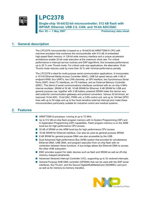
<strong>LPC2378</strong><br />
<strong>Single</strong>-<strong>chip</strong> <strong>16</strong>-<strong>bit</strong>/<strong>32</strong>-<strong>bit</strong> <strong>microcontroller</strong>; <strong>512</strong> <strong>kB</strong> flash with<br />
ISP/IAP, Ethernet, USB 2.0, CAN, and 10-<strong>bit</strong> ADC/DAC<br />
Rev. 02 — 1 May 2007 Preliminary data sheet<br />
The <strong>LPC2378</strong> <strong>microcontroller</strong> is based on a <strong>16</strong>-<strong>bit</strong>/<strong>32</strong>-<strong>bit</strong> ARM7TDMI-S CPU with<br />
real-time emulation that combines the <strong>microcontroller</strong> with <strong>512</strong> <strong>kB</strong> of embedded<br />
high-speed flash memory. A 128-<strong>bit</strong> wide memory interface and a unique accelerator<br />
architecture enable <strong>32</strong>-<strong>bit</strong> code execution at the maximum clock rate. For critical<br />
performance in interrupt service routines and DSP algorithms, this increases performance<br />
up to 30 % over Thumb mode. For critical code size applications, the alternative <strong>16</strong>-<strong>bit</strong><br />
Thumb mode reduces code by more than 30 % with minimal performance penalty.<br />
The <strong>LPC2378</strong> is ideal for multi-purpose serial communication applications. It incorporates<br />
a 10/100 Ethernet Media Access Controller (MAC), USB full speed device with 4 <strong>kB</strong> of<br />
endpoint RAM, four UARTs, two CAN channels, an SPI interface, two Synchronous Serial<br />
Ports (SSP), three I 2 C interfaces, an I 2 S interface, and an External Memory Controller<br />
(EMC). This blend of serial communications interfaces combined with an on-<strong>chip</strong> 4 MHz<br />
internal oscillator, SRAM of <strong>32</strong> <strong>kB</strong>, <strong>16</strong> <strong>kB</strong> SRAM for Ethernet, 8 <strong>kB</strong> SRAM for USB and<br />
general purpose use, together with 2 <strong>kB</strong> battery powered SRAM make this device very<br />
well suited for communication gateways and protocol converters. Various <strong>32</strong>-<strong>bit</strong> timers, an<br />
improved 10-<strong>bit</strong> ADC, 10-<strong>bit</strong> DAC, PWM unit, a CAN control unit, and up to 104 fast GPIO<br />
lines with up to 50 edge and up to four level sensitive external interrupt pins make these<br />
<strong>microcontroller</strong>s particularly suitable for industrial control and medical systems.<br />
■ ARM7TDMI-S processor, running at up to 72 MHz.<br />
■ Up to <strong>512</strong> <strong>kB</strong> on-<strong>chip</strong> flash program memory with In-System Programming (ISP) and<br />
In-Application Programming (IAP) capabilities. Flash program memory is on the ARM<br />
local bus for high performance CPU access.<br />
■ <strong>32</strong> <strong>kB</strong> of SRAM on the ARM local bus for high performance CPU access.<br />
■ <strong>16</strong> <strong>kB</strong> SRAM for Ethernet interface. Can also be used as general purpose SRAM.<br />
■ 8 <strong>kB</strong> SRAM for general purpose DMA use also accessible by the USB.<br />
■ Dual Advanced High-performance Bus (AHB) system that provides for simultaneous<br />
Ethernet DMA, USB DMA, and program execution from on-<strong>chip</strong> flash with no<br />
contention between those functions. A bus bridge allows the Ethernet DMA to access<br />
the other AHB subsystem.<br />
■ EMC provides support for static devices such as flash and SRAM as well as off-<strong>chip</strong><br />
memory mapped peripherals.<br />
■ Advanced Vectored Interrupt Controller (VIC), supporting up to <strong>32</strong> vectored interrupts.<br />
■ General Purpose AHB DMA controller (GPDMA) that can be used with the SSP serial<br />
interfaces, the I 2 S port, and the Secure Digital/MultiMediaCard (SD/MMC) card port,<br />
as well as for memory-to-memory transfers.
NXP Semiconductors <strong>LPC2378</strong><br />
Fast communication <strong>chip</strong><br />
■ Serial Interfaces:<br />
◆ Ethernet MAC with associated DMA controller. These functions reside on an<br />
independent AHB bus.<br />
◆ USB 2.0 full-speed device with on-<strong>chip</strong> PHY and associated DMA controller.<br />
◆ Four UARTs with fractional baud rate generation, one with modem control I/O, one<br />
with IrDA support, all with FIFO.<br />
◆ CAN controller with two channels.<br />
◆ SPI controller.<br />
◆ Two SSP controllers, with FIFO and multi-protocol capabilities. One is an alternate<br />
for the SPI port, sharing its interrupt and pins. These can be used with the GPDMA<br />
controller.<br />
◆ Three I2C-bus interfaces (one with open-drain and two with standard port pins).<br />
◆ I2S (Inter-IC Sound) interface for digital audio input or output. It can be used with<br />
the GPDMA.<br />
■ Other peripherals:<br />
◆ SD/MMC memory card interface.<br />
◆ 104 General purpose I/O pins with configurable pull-up/down resistors.<br />
◆ 10-<strong>bit</strong> ADC with input multiplexing among 8 pins.<br />
◆ 10-<strong>bit</strong> DAC.<br />
◆ Four general purpose timers/counters with 8 capture inputs and 10 compare<br />
outputs. Each timer block has an external count input.<br />
◆ One PWM/timer block with support for three-phase motor control. The PWM has<br />
two external count inputs.<br />
◆ Real-Time Clock (RTC) with separate power pin, clock source can be the RTC<br />
oscillator or the APB clock.<br />
◆ 2 <strong>kB</strong> SRAM powered from the RTC power pin, allowing data to be stored when the<br />
rest of the <strong>chip</strong> is powered off.<br />
◆ WatchDog Timer (WDT). The WDT can be clocked from the internal RC oscillator,<br />
the RTC oscillator, or the APB clock.<br />
■ Standard ARM test/debug interface for compatibility with existing tools.<br />
■ Emulation trace module supports real-time trace.<br />
■ <strong>Single</strong> 3.3 V power supply (3.0 V to 3.6 V).<br />
■ Three reduced power modes: idle, sleep, and power-down.<br />
■ Four external interrupt inputs configurable as edge/level sensitive. All pins on PORT0<br />
and PORT2 can be used as edge sensitive interrupt sources.<br />
■ Processor wake-up from Power-down mode via any interrupt able to operate during<br />
Power-down mode (includes external interrupts, RTC interrupt, USB activity, Ethernet<br />
wake-up interrupt).<br />
■ Two independent power domains allow fine tuning of power consumption based on<br />
needed features.<br />
■ Each peripheral has its own clock divider for further power saving.<br />
■ Brownout detect with separate thresholds for interrupt and forced reset.<br />
■ On-<strong>chip</strong> power-on reset.<br />
■ On-<strong>chip</strong> crystal oscillator with an operating range of 1 MHz to 24 MHz.<br />
■ 4 MHz internal RC oscillator trimmed to 1 % accuracy that can optionally be used as<br />
the system clock. When used as the CPU clock, does not allow CAN and USB to run.<br />
<strong>LPC2378</strong>_2 © NXP B.V. 2007. All rights reserved.<br />
Preliminary data sheet Rev. 02 — 1 May 2007 2 of 53
NXP Semiconductors <strong>LPC2378</strong><br />
3. Applications<br />
Fast communication <strong>chip</strong><br />
■ On-<strong>chip</strong> PLL allows CPU operation up to the maximum CPU rate without the need for<br />
a high frequency crystal. May be run from the main oscillator, the internal RC<br />
oscillator, or the RTC oscillator.<br />
■ Boundary scan for simplified board testing.<br />
■ Versatile pin function selections allow more possibilities for using on-<strong>chip</strong> peripheral<br />
functions.<br />
■ Industrial control<br />
■ Medical systems<br />
■ Protocol converter<br />
■ Communications<br />
4. Ordering information<br />
Table 1. Ordering information<br />
Type number Package<br />
Name Description Version<br />
<strong>LPC2378</strong>FBD144 LQFP144 plastic low profile quad flat package; 144 leads; body 20 × 20 × 1.4 mm SOT486-1<br />
Table 2. Ordering options<br />
Type number Flash<br />
(<strong>kB</strong>)<br />
4.1 Ordering options<br />
Local bus<br />
SRAM (<strong>kB</strong>) External bus Ether<br />
net<br />
Ethernet buffer<br />
<strong>LPC2378</strong>FBD144 <strong>512</strong> <strong>32</strong> <strong>16</strong> 8 2 58 MiniBus: 8 data, <strong>16</strong><br />
address, and 2 <strong>chip</strong><br />
select lines<br />
GP/USB<br />
RTC<br />
Total<br />
USB<br />
device<br />
+ 4 <strong>kB</strong><br />
FIFO<br />
<strong>LPC2378</strong>_2 © NXP B.V. 2007. All rights reserved.<br />
Preliminary data sheet Rev. 02 — 1 May 2007 3 of 53<br />
CAN channels<br />
SD/<br />
MMC<br />
GP<br />
DMA<br />
ADC channels<br />
DAC channels<br />
Temp<br />
range<br />
RMII yes 2 yes yes 8 1 −40 °C to<br />
+85 °C
NXP Semiconductors <strong>LPC2378</strong><br />
5. Block diagram<br />
P0, P1, P2,<br />
P3, P4<br />
RMII(8)<br />
EINT3 to EINT0<br />
P0, P2<br />
2 · CAP0/CAP1/<br />
CAP2/CAP3<br />
4 · MAT2,<br />
2 · MAT0/MAT1/<br />
MAT3<br />
6 · PWM1<br />
2 · PCAP1<br />
P0, P1<br />
8 · AD0<br />
AOUT<br />
VBAT<br />
power domain 2<br />
RTCX1<br />
RTCX2<br />
ALARM<br />
<strong>LPC2378</strong><br />
HIGH-SPEED<br />
GPI/O<br />
104 PINS<br />
TOTAL<br />
ETHERNET<br />
MAC WITH<br />
DMA<br />
Fig 1. <strong>LPC2378</strong> block diagram<br />
<strong>32</strong> <strong>kB</strong><br />
SRAM<br />
PWM1<br />
LEGACY GPI/O<br />
56 PINS TOTAL<br />
<strong>512</strong> <strong>kB</strong><br />
FLASH<br />
INTERNAL<br />
CONTROLLERS<br />
<strong>16</strong> <strong>kB</strong><br />
SRAM<br />
FLASH<br />
EXTERNAL INTERRUPTS<br />
CAPTURE/COMPARE<br />
TIMER0/TIMER1/<br />
TIMER2/TIMER3<br />
A/D CONVERTER<br />
D/A CONVERTER<br />
2 <strong>kB</strong> BATTERY RAM<br />
RTC<br />
OSCILLATOR<br />
SRAM<br />
REAL-<br />
TIME<br />
CLOCK<br />
WATCHDOG TIMER<br />
SYSTEM CONTROL<br />
TMS TDI trace signals<br />
TRST TCK TDO<br />
EXTIN0 DBGEN<br />
AHB<br />
BRIDGE<br />
TEST/DEBUG<br />
INTERFACE<br />
ARM7TDMI-S<br />
EXTERNAL<br />
MEMORY<br />
CONTROLLER<br />
Fast communication <strong>chip</strong><br />
002aac574<br />
<strong>LPC2378</strong>_2 © NXP B.V. 2007. All rights reserved.<br />
Preliminary data sheet Rev. 02 — 1 May 2007 4 of 53<br />
EMULATION<br />
TRACE MODULE<br />
AHB<br />
BRIDGE<br />
MASTER AHB TO SLAVE<br />
PORT APB BRIDGE PORT<br />
AHB TO<br />
APB BRIDGE<br />
PLL<br />
system<br />
clock<br />
RESET<br />
VECTORED<br />
INTERRUPT<br />
CONTROLLER<br />
AHB2 AHB1<br />
XTAL1<br />
XTAL2 VDD(3V3)<br />
8 <strong>kB</strong><br />
SRAM<br />
SYSTEM<br />
FUNCTIONS<br />
INTERNAL RC<br />
OSCILLATOR<br />
D[7:0]<br />
A[15:0]<br />
I2SRX_CLK<br />
I2STX_CLK<br />
I2SRX_WS<br />
I2STX_WS<br />
I2SRX_SDA<br />
I2STX_SDA<br />
SCK, SCK0<br />
MOSI, MOSI0<br />
MISO, MISO0<br />
SSEL, SSEL1<br />
SCK1<br />
MOSI1<br />
MIS01<br />
SSEL1<br />
MCICLK, MCIPWR<br />
TXD0, TXD2, TXD3<br />
RXD0, RXD2, RXD3<br />
TXD1<br />
RXD1<br />
UART1 DTR1, RTS1<br />
DSR1, CTS1, DCD1,<br />
RI1<br />
CAN1, CAN2<br />
VDDA<br />
USB WITH<br />
4 <strong>kB</strong> RAM<br />
AND DMA<br />
GP DMA<br />
CONTROLLER<br />
I 2 S INTERFACE<br />
SPI, SSP0 INTERFACE<br />
SSP1 INTERFACE<br />
SD/MMC CARD<br />
INTERFACE<br />
UART0, UART2, UART3<br />
VREF<br />
VSSA, VSS<br />
VDD(DCDC)(3V3)<br />
WE, OE, CS0, CS1<br />
VBUS<br />
2 · USB_D+/USB_D-<br />
2 · USB_CONNECT<br />
2 · USB_UP_LED<br />
MCICMD,<br />
MCIDAT[3:0]<br />
RD1, RD2<br />
TD1, TD2<br />
SCL0, SCL1, SCL2<br />
I2C0, I2C1, I2C2 SDA0, SDA1, SDA2
NXP Semiconductors <strong>LPC2378</strong><br />
6. Pinning information<br />
6.1 Pinning<br />
Fig 2. <strong>LPC2378</strong> pinning<br />
6.2 Pin description<br />
1<br />
36<br />
144<br />
37<br />
<strong>LPC2378</strong>FBD144<br />
Fast communication <strong>chip</strong><br />
<strong>LPC2378</strong>_2 © NXP B.V. 2007. All rights reserved.<br />
Preliminary data sheet Rev. 02 — 1 May 2007 5 of 53<br />
109<br />
72<br />
108<br />
73<br />
002aac584<br />
Table 3. Pin description<br />
Symbol Pin Type Description<br />
P0[0] to P0[31] I/O Port 0: Port 0 is a <strong>32</strong>-<strong>bit</strong> I/O port with individual direction controls for each <strong>bit</strong>. The<br />
operation of port 0 pins depends upon the pin function selected via the Pin Connect<br />
block.<br />
P0[0]/RD1/TXD/ 66<br />
SDA1<br />
[1] I/O P0[0] — General purpose digital input/output pin.<br />
I RD1 — CAN1 receiver input.<br />
O TXD3 — Transmitter output for UART3.<br />
I/O SDA1 — I2C1 data input/output (this is not an open-drain pin).<br />
P0[1]/TD1/RXD3/ 67<br />
SCL1<br />
[1] I/O P0[1] — General purpose digital input/output pin.<br />
O TD1 — CAN1 transmitter output.<br />
I RXD3 — Receiver input for UART3.<br />
I/O SCL1 — I2C1 clock input/output (this is not an open-drain pin).<br />
P0[2]/TXD0 141 [1] I/O P0[2] — General purpose digital input/output pin.<br />
O TXD0 — Transmitter output for UART0.<br />
P0[3]/RXD0 142 [1] I/O P0[3] — General purpose digital input/output pin.<br />
I RXD0 — Receiver input for UART0.<br />
P0[4]/<br />
1<strong>16</strong><br />
I2SRX_CLK/<br />
RD2/CAP2[0]<br />
[1] I/O P0[4] — General purpose digital input/output pin.<br />
I/O I2SRX_CLK — Receive Clock. It is driven by the master and received by the slave.<br />
Corresponds to the signal SCK in the I2S-bus specification.<br />
I RD2 — CAN2 receiver input.<br />
I CAP2[0] — Capture input for Timer 2, channel 0.
NXP Semiconductors <strong>LPC2378</strong><br />
Table 3. Pin description …continued<br />
Symbol Pin Type Description<br />
P0[5]/<br />
I2SRX_WS/<br />
TD2/CAP2[1]<br />
P0[6]/<br />
I2SRX_SDA/<br />
SSEL1/MAT2[0]<br />
P0[7]/<br />
I2STX_CLK/<br />
SCK1/MAT2[1]<br />
P0[8]/<br />
I2STX_WS/<br />
MISO1/MAT2[2]<br />
P0[9]/<br />
I2STX_SDA/<br />
MOSI1/MAT2[3]<br />
P0[10]/TXD2/<br />
SDA2/MAT3 [0]<br />
P0[11]/RXD2/<br />
SCL2/MAT3[1]<br />
P0[12]/MISO1/<br />
AD0[6]<br />
P0[13]/<br />
USB_UP_LED2/<br />
MOSI1/AD0[7]<br />
Fast communication <strong>chip</strong><br />
115 [1] I/O P0[5] — General purpose digital input/output pin.<br />
I/O I2SRX_WS — Receive Word Select. It is driven by the master and received by the<br />
slave. Corresponds to the signal WS in the I2S-bus specification.<br />
O TD2 — CAN2 transmitter output.<br />
I CAP2[1] — Capture input for Timer 2, channel 1.<br />
113 [1] I/O P0[6] — General purpose digital input/output pin.<br />
I/O I2SRX_SDA — Receive data. It is driven by the transmitter and read by the receiver.<br />
Corresponds to the signal SD in the I2S-bus specification.<br />
I/O SSEL1 — Slave Select for SSP1.<br />
O MAT2[0] — Match output for Timer 2, channel 0.<br />
112 [1] I/O P0[7] — General purpose digital input/output pin.<br />
I/O I2STX_CLK — Transmit Clock. It is driven by the master and received by the slave.<br />
Corresponds to the signal SCK in the I2S-bus specification.<br />
I/O SCK1 — Serial Clock for SSP1.<br />
O MAT2[1] — Match output for Timer 2, channel 1.<br />
111 [1] I/O P0[8] — General purpose digital input/output pin.<br />
I/O I2STX_WS — Transmit Word Select. It is driven by the master and received by the<br />
slave. Corresponds to the signal WS in the I2S-bus specification.<br />
I/O MISO1 — Master In Slave Out for SSP1.<br />
O MAT2[2] — Match output for Timer 2, channel 2.<br />
109 [1] I/O P0[9] — General purpose digital input/output pin.<br />
I/O I2STX_SDA — Transmit data. It is driven by the transmitter and read by the receiver.<br />
Corresponds to the signal SD in the I2S-bus specification.<br />
I/O MOSI1 — Master Out Slave In for SSP1.<br />
O MAT2[3] — Match output for Timer 2, channel 3.<br />
69 [1] I/O P0[10] — General purpose digital input/output pin.<br />
O TXD2 — Transmitter output for UART2.<br />
I/O SDA2 — I2C2 data input/output (this is not an open-drain pin).<br />
O MAT3[0] — Match output for Timer 3, channel 0.<br />
70 [1] I/O P0[11] — General purpose digital input/output pin.<br />
I RXD2 — Receiver input for UART2.<br />
I/O SCL2 — I2C2 clock input/output (this is not an open-drain pin).<br />
O MAT3[1] — Match output for Timer 3, channel 1.<br />
29 [2] I/O P0[12] — General purpose digital input/output pin.<br />
I/O MISO1 — Master In Slave Out for SSP1.<br />
I AD0[6] — A/D converter 0, input 6.<br />
<strong>32</strong> [2] I/O P0[13] — General purpose digital input/output pin.<br />
O USB_UP_LED2 — USB2 Good Link LED indicator. It is LOW when device is<br />
configured (non-control endpoints enabled). It is HIGH when the device is not<br />
configured or during global suspend.<br />
I/O MOSI1 — Master Out Slave In for SSP1.<br />
I AD0[7] — A/D converter 0, input 7.<br />
<strong>LPC2378</strong>_2 © NXP B.V. 2007. All rights reserved.<br />
Preliminary data sheet Rev. 02 — 1 May 2007 6 of 53
NXP Semiconductors <strong>LPC2378</strong><br />
Table 3. Pin description …continued<br />
Symbol Pin Type Description<br />
P0[14]/<br />
USB_CONNECT2/<br />
SSEL1<br />
P0[15]/TXD1/<br />
SCK0/SCK<br />
P0[<strong>16</strong>]/RXD1/<br />
SSEL0/SSEL<br />
P0[17]/CTS1/<br />
MISO0/MISO<br />
P0[18]/DCD1/<br />
MOSI0/MOSI<br />
P0[19]/DSR1/<br />
MCICLK/SDA1<br />
P0[20]/DTR1/<br />
MCICMD/SCL1<br />
P0[21]/RI1/<br />
MCIPWR/RD1<br />
P0[22]/RTS1/<br />
MCIDAT0/TD1<br />
P0[23]/AD0[0]/<br />
I2SRX_CLK/<br />
CAP3[0]<br />
Fast communication <strong>chip</strong><br />
48 [1] I/O P0[14] — General purpose digital input/output pin.<br />
O USB_CONNECT2 — USB2 Soft Connect control. Signal used to switch an external<br />
1.5 kΩ resistor under software control. Used with the SoftConnect USB feature.<br />
I/O SSEL1 — Slave Select for SSP1.<br />
89 [1] I/O P0[15] — General purpose digital input/output pin.<br />
O TXD1 — Transmitter output for UART1.<br />
I/O SCK0 — Serial clock for SSP0.<br />
I/O SCK — Serial clock for SPI.<br />
90 [1] I/O P0 [<strong>16</strong>] — General purpose digital input/output pin.<br />
I RXD1 — Receiver input for UART1.<br />
I/O SSEL0 — Slave Select for SSP0.<br />
I/O SSEL — Slave Select for SPI.<br />
87 [1] I/O P0[17] — General purpose digital input/output pin.<br />
I CTS1 — Clear to Send input for UART1.<br />
I/O MISO0 — Master In Slave Out for SSP0.<br />
I/O MISO — Master In Slave Out for SPI.<br />
86 [1] I/O P0[18] — General purpose digital input/output pin.<br />
I DCD1 — Data Carrier Detect input for UART1.<br />
I/O MOSI0 — Master Out Slave In for SSP0.<br />
I/O MOSI — Master Out Slave In for SPI.<br />
85 [1] I/O P0[19] — General purpose digital input/output pin.<br />
I DSR1 — Data Set Ready input for UART1.<br />
O MCICLK — Clock output line for SD/MMC interface.<br />
I/O SDA1 — I2C1 data input/output (this is not an open-drain pin).<br />
83 [1] I/O P0[20] — General purpose digital input/output pin.<br />
O DTR1 — Data Terminal Ready output for UART1.<br />
I MCICMD — Command line for SD/MMC interface.<br />
I/O SCL1 — I2C1 clock input/output (this is not an open-drain pin).<br />
82 [1] I/O P0[21] — General purpose digital input/output pin.<br />
I RI1 — Ring Indicator input for UART1.<br />
O MCIPWR — Power Supply Enable for external SD/MMC power supply.<br />
I RD1 — CAN1 receiver input.<br />
80 [1] I/O P0[22] — General purpose digital input/output pin.<br />
O RTS1 — Request to Send output for UART1.<br />
O MCIDAT0 — Data line for SD/MMC interface.<br />
O TD1 — CAN1 transmitter output.<br />
13 [2] I/O P0[23] — General purpose digital input/output pin.<br />
I AD0[0] — A/D converter 0, input 0.<br />
I/O I2SRX_CLK — Receive Clock. It is driven by the master and received by the slave.<br />
Corresponds to the signal SCK in the I2S-bus specification.<br />
I CAP3[0] — Capture input for Timer 3, channel 0.<br />
<strong>LPC2378</strong>_2 © NXP B.V. 2007. All rights reserved.<br />
Preliminary data sheet Rev. 02 — 1 May 2007 7 of 53
NXP Semiconductors <strong>LPC2378</strong><br />
Table 3. Pin description …continued<br />
Symbol Pin Type Description<br />
P0[24]/AD0[1]/<br />
I2SRX_WS/<br />
CAP3[1]<br />
P0[25]/AD0[2]/<br />
I2SRX_SDA/<br />
TXD3<br />
Fast communication <strong>chip</strong><br />
11 [3] I/O P0[24] — General purpose digital input/output pin.<br />
I AD0[1] — A/D converter 0, input 1.<br />
I/O I2SRX_WS — Receive Word Select. It is driven by the master and received by the<br />
slave. Corresponds to the signal WS in the I2S-bus specification.<br />
I CAP3[1] — Capture input for Timer 3, channel 1.<br />
10 [2] I/O P0[25] — General purpose digital input/output pin.<br />
I AD0[2] — A/D converter 0, input 2.<br />
I/O I2SRX_SDA — Receive data. It is driven by the transmitter and read by the receiver.<br />
Corresponds to the signal SD in the I2S-bus specification.<br />
O TXD3 — Transmitter output for UART3.<br />
P0[26]/AD0[3]/ 8<br />
AOUT/RXD3<br />
[2] I/O P0[26] — General purpose digital input/output pin.<br />
I AD0[3] — ]A/D converter 0, input 3.<br />
O AOUT — D/A converter output.<br />
I RXD3 — Receiver input for UART3.<br />
P0[27]/SDA0 35 [4] I/O P0[27] — General purpose digital input/output pin.<br />
I/O SDA0 — I2C0 data input/output. Open-drain output (for I2C-bus compliance).<br />
P0[28]/SCL0 34 [4] I/O P0[28] — General purpose digital input/output pin.<br />
I/O SCL0 — I2C0 clock input/output. Open-drain output (for I2C-bus compliance).<br />
P0[29]/USB_D+1 42 [5] I/O P0[29] — General purpose digital input/output pin.<br />
I/O USB_D+1 — USB1 port bidirectional D+ line.<br />
P0[30]/USB_D−1 43 [5] I/O P0[30] — General purpose digital input/output pin.<br />
I/O USB_D−1 — USB1 port bidirectional D− line.<br />
P0[31]/USB_D+2 36 [5] I/O P0[31] — General purpose digital input/output pin.<br />
I/O USB_D+2 — USB2 port bidirectional D+ line.<br />
P1[0] to P1[31] I/O Port 1: Port 1 is a <strong>32</strong>-<strong>bit</strong> I/O port with individual direction controls for each <strong>bit</strong>. The<br />
operation of port 1 pins depends upon the pin function selected via the Pin Connect<br />
block. Pins 2, 3, 5, 6, 7, 11, 12, and 13 of this port are not available.<br />
P1[0]/<br />
136<br />
ENET_TXD0<br />
[1] I/O P1[0] — General purpose digital input/output pin.<br />
O ENET_TXD0 — Ethernet transmit data 0.<br />
P1[1]/<br />
135<br />
ENET_TXD1<br />
[1] I/O P1[1] — General purpose digital input/output pin.<br />
O ENET_TXD1 — Ethernet transmit data 1.<br />
P1[4]/<br />
133<br />
ENET_TX_EN<br />
[1] I/O P1[4] — General purpose digital input/output pin.<br />
O ENET_TX_EN — Ethernet transmit data enable.<br />
P1[8]/<br />
1<strong>32</strong><br />
ENET_CRS<br />
[1] I/O P1[8] — General purpose digital input/output pin.<br />
I ENET_CRS — Ethernet carrier sense.<br />
P1[9]/<br />
131<br />
ENET_RXD0<br />
[1] I/O P1[9] — General purpose digital input/output pin.<br />
I ENET_RXD0 — Ethernet receive data.<br />
P1[10]/<br />
129<br />
ENET_RXD1<br />
[1] I/O P1[10] — General purpose digital input/output pin.<br />
I ENET_RXD1 — Ethernet receive data.<br />
P1[14]/<br />
128<br />
ENET_RX_ER<br />
[1] I/O P1[14] — General purpose digital input/output pin.<br />
I ENET_RX_ER — Ethernet receive error.<br />
<strong>LPC2378</strong>_2 © NXP B.V. 2007. All rights reserved.<br />
Preliminary data sheet Rev. 02 — 1 May 2007 8 of 53
NXP Semiconductors <strong>LPC2378</strong><br />
Table 3. Pin description …continued<br />
Symbol Pin Type Description<br />
P1[15]/<br />
ENET_REF_CLK<br />
P1[<strong>16</strong>]/<br />
ENET_MDC<br />
P1[17]/<br />
ENET_MDIO<br />
126 [1] I/O P1[15] — General purpose digital input/output pin.<br />
I ENET_REF_CLK/ENET_RX_CLK — Ethernet receiver clock.<br />
125 [1] I/O P1[<strong>16</strong>] — General purpose digital input/output pin.<br />
I ENET_MDC — Ethernet MIIM clock.<br />
123 [1] I/O P1[17] — General purpose digital input/output pin.<br />
I/O ENET_MDIO — Ethernet MI data input and output.<br />
Fast communication <strong>chip</strong><br />
P1[18]/<br />
46<br />
USB_UP_LED1/<br />
PWM1[1]/<br />
CAP1[0]<br />
[1] I/O P1[18] — General purpose digital input/output pin.<br />
O USB_UP_LED1 — USB1 port Good Link LED indicator. It is LOW when device is<br />
configured (non-control endpoints enabled). It is HIGH when the device is not<br />
configured or during global suspend.<br />
O PWM1[1] — Pulse Width Modulator 1, channel 1 output.<br />
I CAP1[0] — Capture input for Timer 1, channel 0.<br />
P1[19]/CAP1[1] 47 [1] I/O P1[19] — General purpose digital input/output pin.<br />
I CAP1[1] — Capture input for Timer 1, channel 1.<br />
P1[20]/PWM1[2]/ 49<br />
SCK0<br />
[1] I/O P1[20] — General purpose digital input/output pin.<br />
O PWM1[2] — Pulse Width Modulator 1, channel 2 output.<br />
I/O SCK0 — Serial clock for SSP0.<br />
P1[21]/PWM1[3]/ 50<br />
SSEL0<br />
[1] I/O P1[21] — General purpose digital input/output pin.<br />
O PWM1[3] — Pulse Width Modulator 1, channel 3 output.<br />
I/O SSEL0 — Slave Select for SSP0.<br />
P1[22]/MAT1[0] 51 [1] I/O P1[22] — General purpose digital input/output pin.<br />
O MAT1[0] — Match output for Timer 1, channel 0.<br />
P1[23]/PWM1[4]/ 53<br />
MISO0<br />
[1] I/O P1[23] — General purpose digital input/output pin.<br />
O PWM1[4] — Pulse Width Modulator 1, channel 4 output.<br />
I/O MISO0 — Master In Slave Out for SSP0.<br />
P1[24]/PWM1[5]/ 54<br />
MOSI0<br />
[1] I/O P1[24] — General purpose digital input/output pin.<br />
O PWM1[5] — Pulse Width Modulator 1, channel 5 output.<br />
I/O MOSI0 — Master Out Slave in for SSP0.<br />
P1[25]/MAT1[1] 56 [1] I/O P1[25] — General purpose digital input/output pin.<br />
O MAT1[1] — Match output for Timer 1, channel 1.<br />
P1[26]/PWM1[6]/ 57<br />
CAP0[0]<br />
[1] I/O P1[26] — General purpose digital input/output pin.<br />
O PWM1[6] — Pulse Width Modulator 1, channel 6 output.<br />
I CAP0[0] — Capture input for Timer 0, channel 0.<br />
P1[27]/CAP0[1] 61 [1] I/O P1[27] — General purpose digital input/output pin.<br />
I CAP0[1] — Capture input for Timer 0, channel 1.<br />
P1[28]/<br />
63<br />
PCAP1[0]/<br />
MAT0[0]<br />
[1] I/O P1[28] — General purpose digital input/output pin.<br />
I<br />
O<br />
PCAP1[0] — Capture input for PWM1, channel 0.<br />
MAT0[0] — Match output for Timer 0, channel 0.<br />
P1[29]/<br />
64<br />
PCAP1[1]/<br />
MAT0[1]<br />
[1] I/O P1[29] — General purpose digital input/output pin.<br />
I<br />
O<br />
PCAP1[1] — Capture input for PWM1, channel 1.<br />
MAT0[1] — Match output for Timer 0, channel 0.<br />
<strong>LPC2378</strong>_2 © NXP B.V. 2007. All rights reserved.<br />
Preliminary data sheet Rev. 02 — 1 May 2007 9 of 53
NXP Semiconductors <strong>LPC2378</strong><br />
Fast communication <strong>chip</strong><br />
P1[30]/<br />
30<br />
VBUS/AD0[4]<br />
[2] I/O P1[30] — General purpose digital input/output pin.<br />
I VBUS — Indicates the presence of USB bus power.<br />
Note: This signal must be HIGH for USB reset to occur.<br />
I AD0[4] — A/D converter 0, input 4.<br />
P1[31]/SCK1/ 28<br />
AD0[5]<br />
[2] I/O P1[31] — General purpose digital input/output pin.<br />
I/O SCK1 — Serial Clock for SSP1.<br />
I AD0[5] — A/D converter 0, input 5.<br />
P2[0] to P2[31] I/O Port 2: Port 2 is a <strong>32</strong> <strong>bit</strong> I/O port with individual direction controls for each <strong>bit</strong>. The<br />
operation of port 2 pins depends upon the pin function selected via the Pin Connect<br />
block. Pins 14 through 31 of this port are not available.<br />
P2[0]/PWM1[1]/ 107<br />
TXD1/<br />
TRACECLK<br />
[1] I/O P2[0] — General purpose digital input/output pin.<br />
O<br />
O<br />
PWM1[1] — Pulse Width Modulator 1, channel 1 output.<br />
TXD1 — Transmitter output for UART1.<br />
O TRACECLK — Trace Clock.<br />
P2[1]/PWM1[2]/ 106<br />
RXD1/<br />
PIPESTAT0<br />
[1] I/O P2[1] — General purpose digital input/output pin.<br />
O<br />
I<br />
PWM1[2] — Pulse Width Modulator 1, channel 2 output.<br />
RXD1 — Receiver input for UART1.<br />
O PIPESTAT0 — Pipeline Status, <strong>bit</strong> 0.<br />
P2[2]/PWM1[3]/ 105<br />
CTS1/<br />
PIPESTAT1<br />
[1] I/O P2[2] — General purpose digital input/output pin.<br />
O<br />
I<br />
PWM1[3] — Pulse Width Modulator 1, channel 3 output.<br />
CTS1 — Clear to Send input for UART1.<br />
O PIPESTAT1 — Pipeline Status, <strong>bit</strong> 1.<br />
P2[3]/PWM1[4]/ 100<br />
DCD1/<br />
PIPESTAT2<br />
[1] I/O P2[3] — General purpose digital input/output pin.<br />
O<br />
I<br />
PWM1[4] — Pulse Width Modulator 1, channel 4 output.<br />
DCD1 — Data Carrier Detect input for UART1.<br />
O PIPESTAT2 — Pipeline Status, <strong>bit</strong> 2.<br />
P2[4]/PWM1[5]/ 99<br />
DSR1/<br />
TRACESYNC<br />
[1] I/O P2[4] — General purpose digital input/output pin.<br />
O<br />
I<br />
PWM1[5] — Pulse Width Modulator 1, channel 5 output.<br />
DSR1 — Data Set Ready input for UART1.<br />
O TRACESYNC — Trace Synchronization.<br />
P2[5]/PWM1[6]/ 97<br />
DTR1/<br />
TRACEPKT0<br />
[1] I/O P2[5] — General purpose digital input/output pin.<br />
O<br />
O<br />
PWM1[6] — Pulse Width Modulator 1, channel 6 output.<br />
DTR1 — Data Terminal Ready output for UART1.<br />
O TRACEPKT0 — Trace Packet, <strong>bit</strong> 0.<br />
P2[6]/PCAP1[0]/ 96<br />
RI1/<br />
TRACEPKT1<br />
[1] Table 3. Pin description …continued<br />
Symbol Pin Type Description<br />
I/O P2[6] — General purpose digital input/output pin.<br />
I<br />
I<br />
PCAP1[0] — Capture input for PWM1, channel 0.<br />
RI1 — Ring Indicator input for UART1.<br />
O TRACEPKT1 — Trace Packet, <strong>bit</strong> 1.<br />
<strong>LPC2378</strong>_2 © NXP B.V. 2007. All rights reserved.<br />
Preliminary data sheet Rev. 02 — 1 May 2007 10 of 53
NXP Semiconductors <strong>LPC2378</strong><br />
Fast communication <strong>chip</strong><br />
P2[7]/RD2/ 95<br />
RTS1/<br />
TRACEPKT2<br />
[1] I/O P2[7] — General purpose digital input/output pin.<br />
I<br />
O<br />
RD2 — CAN2 receiver input.<br />
RTS1 — Request to Send output for UART1.<br />
O TRACEPKT2 — Trace Packet, <strong>bit</strong> 2.<br />
P2[8]/TD2/ 93<br />
TXD2/<br />
TRACEPKT3<br />
[1] I/O P2[8] — General purpose digital input/output pin.<br />
O<br />
O<br />
TD2 — CAN2 transmitter output.<br />
TXD2 — Transmitter output for UART2.<br />
O TRACEPKT3 — Trace Packet, <strong>bit</strong> 3.<br />
P2[9]/<br />
92<br />
USB_CONNECT1/<br />
RXD2/<br />
EXTIN0<br />
[1] I/O P2[9] — General purpose digital input/output pin.<br />
O<br />
I<br />
USB_CONNECT1 — USB1 Soft Connect control. Signal used to switch an external<br />
1.5 kΩ resistor under the software control. Used with the SoftConnect USB feature.<br />
RXD2 — Receiver input for UART2.<br />
I EXTIN0 — External Trigger Input.<br />
P2[10]/EINT0 76 [6] I/O P2[10] — General purpose digital input/output pin.<br />
Note: LOW on this pin while RESET is LOW forces on-<strong>chip</strong> boot-loader to take over<br />
control of the part after a reset.<br />
I EINT0 — External interrupt 0 input.<br />
P2[11]/EINT1/ 75<br />
MCIDAT1/<br />
I2STX_CLK<br />
[6] I/O P2[11] — General purpose digital input/output pin.<br />
I<br />
O<br />
EINT1 — External interrupt 1 input.<br />
MCIDAT1 — Data line for SD/MMC interface.<br />
I/O I2STX_CLK — Transmit Clock. It is driven by the master and received by the slave.<br />
Corresponds to the signal SCK in the I2S-bus specification.<br />
P2[12]/EINT2/ 73<br />
MCIDAT2/<br />
I2STX_WS<br />
[6] I/O P2[12] — General purpose digital input/output pin.<br />
I<br />
O<br />
EINT2 — External interrupt 2 input.<br />
MCIDAT2 — Data line for SD/MMC interface.<br />
I/O I2STX_WS — Transmit Word Select. It is driven by the master and received by the<br />
slave. Corresponds to the signal WS in the I2S-bus specification.<br />
P2[13]/EINT3/ 71<br />
MCIDAT3/<br />
I2STX_SDA<br />
[6] I/O P2[13] — General purpose digital input/output pin.<br />
I<br />
O<br />
EINT3 — External interrupt 3 input.<br />
MCIDAT3 — Data line for SD/MMC interface.<br />
I/O I2STX_SDA — Transmit data. It is driven by the transmitter and read by the receiver.<br />
Corresponds to the signal SD in the I2S-bus specification.<br />
P3[0] to P3[31] I/O Port 3: Port 3 is a <strong>32</strong> <strong>bit</strong> I/O port with individual direction controls for each <strong>bit</strong>. The<br />
operation of port 3 pins depends upon the pin function selected via the Pin Connect<br />
block. Pins 8 through 22, and 27 through 31 of this port are not available.<br />
P3[0]/D0 137 [1] I/O P3[0] — General purpose digital input/output pin.<br />
I/O D0 — External memory data line 0.<br />
P3[1]/D1 140 [1] I/O P3[1] — General purpose digital input/output pin.<br />
I/O D1 — External memory data line 1.<br />
P3[2]/D2 144 [1] I/O P3[2] — General purpose digital input/output pin.<br />
I/O D2 — External memory data line 2.<br />
P3[3]/D3 2 [1] Table 3. Pin description …continued<br />
Symbol Pin Type Description<br />
I/O P3[3] — General purpose digital input/output pin.<br />
I/O D3 — External memory data line 3.<br />
<strong>LPC2378</strong>_2 © NXP B.V. 2007. All rights reserved.<br />
Preliminary data sheet Rev. 02 — 1 May 2007 11 of 53
NXP Semiconductors <strong>LPC2378</strong><br />
Table 3. Pin description …continued<br />
Symbol Pin Type Description<br />
Fast communication <strong>chip</strong><br />
P3[4]/D4 9 [1] I/O P3[4] — General purpose digital input/output pin.<br />
I/O D4 — External memory data line 4.<br />
P3[5]/D5 12 [1] I/O P3[5] — General purpose digital input/output pin.<br />
I/O D5 — External memory data line 5.<br />
P3[6]/D6 <strong>16</strong> [1] I/O P3[6] — General purpose digital input/output pin.<br />
I/O D6 — External memory data line 6.<br />
P3[7]/D7 19 [1] I/O P3[7] — General purpose digital input/output pin.<br />
I/O D7 — External memory data line 7.<br />
P3[23]/CAP0[0]/ 45<br />
PCAP1[0]<br />
[1] I/O P3[23] — General purpose digital input/output pin.<br />
I CAP0[0] — Capture input for Timer 0, channel 0.<br />
I PCAP1[0] — Capture input for PWM1, channel 0.<br />
P3[24]/CAP0[1]/ 40<br />
PWM1[1]<br />
[1] I/O P3[24] — General purpose digital input/output pin.<br />
I CAP0[1] — Capture input for Timer 0, channel 1.<br />
O PWM1[1] — Pulse Width Modulator 1, output 1.<br />
P3[25]/MAT0[0]/ 39<br />
PWM1[2]<br />
[1] I/O P3[25] — General purpose digital input/output pin.<br />
O MAT0[0] — Match output for Timer 0, channel 0.<br />
O PWM1[2] — Pulse Width Modulator 1, output 2.<br />
P3[26]/MAT0[1]/ 38<br />
PWM1[3]<br />
[1] I/O P3[26] — General purpose digital input/output pin.<br />
O MAT0[1] — Match output for Timer 0, channel 1.<br />
O PWM1[3] — Pulse Width Modulator 1, output 3.<br />
P4[0] to P4[31] I/O Port 4: Port 4 is a <strong>32</strong> <strong>bit</strong> I/O port with individual direction controls for each <strong>bit</strong>. The<br />
operation of port 4 pins depends upon the pin function selected via the Pin Connect<br />
block. Pins <strong>16</strong> through 23, 26, and 27 of this port are not available.<br />
P4[0]/A0 52 [1] I/O P4[0] — ]General purpose digital input/output pin.<br />
I/O A0 — External memory address line 0.<br />
P4[1]/A1 55 [1] I/O P4[1] — General purpose digital input/output pin.<br />
I/O A1 — External memory address line 1.<br />
P4[2]/A2 58 [1] I/O P4[2] — General purpose digital input/output pin.<br />
I/O A2 — External memory address line 2.<br />
P4[3]/A3 68 [1] I/O P4[3] — General purpose digital input/output pin.<br />
I/O A3 — External memory address line 3.<br />
P4[4]/A4 72 [1] I/O P4[4] — General purpose digital input/output pin.<br />
I/O A4 — External memory address line 4.<br />
P4[5]/A5 74 [1] I/O P4[5] — General purpose digital input/output pin.<br />
I/O A5 — External memory address line 5.<br />
P4[6]/A6 78 [1] I/O P4[6] — General purpose digital input/output pin.<br />
I/O A6 — External memory address line 6.<br />
P4[7]/A7 84 [1] I/O P4[7] — General purpose digital input/output pin.<br />
I/O A7 — External memory address line 7.<br />
P4[8]/A8 88 [1] I/O P4[8] — General purpose digital input/output pin.<br />
I/O A8 — External memory address line 8.<br />
<strong>LPC2378</strong>_2 © NXP B.V. 2007. All rights reserved.<br />
Preliminary data sheet Rev. 02 — 1 May 2007 12 of 53
NXP Semiconductors <strong>LPC2378</strong><br />
Table 3. Pin description …continued<br />
Symbol Pin Type Description<br />
Fast communication <strong>chip</strong><br />
P4[9]/A9 91 [1] I/O P4[9] — General purpose digital input/output pin.<br />
I/O A9 — External memory address line 9.<br />
P4[10]/A10 94 [1] I/O P4[10] — General purpose digital input/output pin.<br />
I/O A10 — External memory address line 10.<br />
P4[11]/A11 101 [1] I/O P4[11] — General purpose digital input/output pin.<br />
I/O A11 — External memory address line 11.<br />
P4[12]/A12 104 [1] I/O P4[12] — General purpose digital input/output pin.<br />
I/O A12 — External memory address line 12.<br />
P4[13]/A13 108 [1] I/O P4[13] — General purpose digital input/output pin.<br />
I/O A13 — External memory address line 13.<br />
P4[14]/A14 110 [1] I/O P4[14] — General purpose digital input/output pin.<br />
I/O A14 — External memory address line 14.<br />
P4[15]/A15 120 [1] I/O P4[15] — General purpose digital input/output pin.<br />
I/O A15 — External memory address line 15.<br />
P4[24]/OE 127 [1] I/O P4[24] — General purpose digital input/output pin.<br />
O OE — LOW active Output Enable signal.<br />
P4[25]/WE 124 [1] I/O P4[25] — General purpose digital input/output pin.<br />
O WE — LOW active Write Enable signal.<br />
P4[28]/MAT2[0]/ 118<br />
TXD3<br />
[1] I/O P4 [28] — General purpose digital input/output pin.<br />
O MAT2[0] — Match output for Timer 2, channel 0.<br />
O TXD3 — Transmitter output for UART3.<br />
P4[29]/MAT2[1]/ 122<br />
RXD3<br />
[1] I/O P4[29] — General purpose digital input/output pin.<br />
O MAT2[1] — Match output for Timer 2, channel 1.<br />
I RXD3 — Receiver input for UART3.<br />
P4[30]/CS0 130 [1] I/O P4[30] — General purpose digital input/output pin.<br />
O CS0 — LOW active Chip Select 0 signal.<br />
P4[31]/CS1 134 [1] I/O P4[31] — General purpose digital input/output pin.<br />
O CS1 — LOW active Chip Select 1 signal.<br />
ALARM 26 [8] O ALARM — RTC controlled output. This is a 1.8 V pin. It goes HIGH when a RTC<br />
alarm is generated.<br />
USB_D−2 37 I/O USB_D−2 — USB2 port bidirectional D− line.<br />
DBGEN 6 [1] I DBGEN — JTAG interface control signal. Also used for boundary scanning.<br />
TDO 1 [1] O TDO — Test Data out for JTAG interface.<br />
TDI 3 [1] I TDI — Test Data in for JTAG interface.<br />
TMS 4 [1] I TMS — Test Mode Select for JTAG interface.<br />
TRST 5 [1] I TRST — Test Reset for JTAG interface.<br />
TCK 7 [1] I TCK — Test Clock for JTAG interface.<br />
RTCK 143 [1] I/O RTCK — JTAG interface control signal.<br />
Note: LOW on this pin while RESET is LOW enables ETM pins (P2[9:0]) to operate<br />
as Trace port after reset.<br />
RSTOUT 20 [1] O RSTOUT — This is a 1.8 V pin. LOW on this pin indicates <strong>LPC2378</strong> being in Reset<br />
state.<br />
<strong>LPC2378</strong>_2 © NXP B.V. 2007. All rights reserved.<br />
Preliminary data sheet Rev. 02 — 1 May 2007 13 of 53
NXP Semiconductors <strong>LPC2378</strong><br />
Fast communication <strong>chip</strong><br />
RESET 24 [7] I external reset input: A LOW on this pin resets the device, causing I/O ports and<br />
peripherals to take on their default states, and processor execution to begin at<br />
address 0. TTL with hysteresis, 5 V tolerant.<br />
XTAL1 31 [8] I Input to the oscillator circuit and internal clock generator circuits.<br />
XTAL2 33 [8] O Output from the oscillator amplifier.<br />
RTCX1 23 [8] I Input to the RTC oscillator circuit.<br />
RTCX2 25 [8] O Output from the RTC oscillator circuit.<br />
VSS<br />
22, 44,<br />
59, 65,<br />
79, 103,<br />
117,119,<br />
139 [9]<br />
Table 3. Pin description …continued<br />
Symbol Pin Type Description<br />
I ground: 0 V reference.<br />
VSSA 15 [10] I analog ground: 0 V reference. This should nominally be the same voltage as VSS,<br />
but should be isolated to minimize noise and error.<br />
VDD(3V3)<br />
41, 62,<br />
77, 102,<br />
114,<br />
138 [11]<br />
I 3.3 V supply voltage: This is the power supply voltage for the I/O ports.<br />
n.c. 21, 81,<br />
98 [12]<br />
VDD(DCDC)(3V3) 18, 60,<br />
121 [13]<br />
I Leave these pins unconnected.<br />
I 3.3 V DC-to-DC converter supply voltage: This is the power supply for the on-<strong>chip</strong><br />
DC-to-DC converter only.<br />
VDDA 14 [14] I analog 3.3 V pad supply voltage: This should be nominally the same voltage as<br />
VDD(3V3) but should be isolated to minimize noise and error. This voltage is used to<br />
power the ADC and DAC.<br />
VREF 17 [14] I ADC reference: This should be nominally the same voltage as VDD(3V3) but should<br />
be isolated to minimize noise and error. The level on this pin is used as a reference<br />
for ADC and DAC.<br />
VBAT 27 [14] I RTC power supply: 3.3 V on this pin supplies the power to the RTC.<br />
[1] 5 V tolerant pad providing digital I/O functions with TTL levels and hysteresis.<br />
[2] 5 V tolerant pad providing digital I/O functions (with TTL levels and hysteresis) and analog input. When configured as a DAC input,<br />
digital section of the pad is disabled.<br />
[3] 5 V tolerant pad providing digital I/O with TTL levels and hysteresis and analog output function. When configured as the DAC output,<br />
digital section of the pad is disabled.<br />
[4] Open-drain 5 V tolerant digital I/O I2C-bus 400 kHz specification compatible pad. It requires an external pull-up to provide output<br />
functionality. When power is switched off, this pin connected to the I2C-bus is floating and does not disturb the I2C lines.<br />
[5] Pad provides digital I/O and USB functions. It is designed in accordance with the USB specification, revision 2.0 (Full-speed and<br />
Low-speed mode only).<br />
[6] 5 V tolerant pad with 5 ns glitch filter providing digital I/O functions with TTL levels and hysteresis.<br />
[7] 5 V tolerant pad with 20 ns glitch filter providing digital I/O function with TTL levels and hysteresis.<br />
[8] Pad provides special analog functionality.<br />
[9] Pad provides special analog functionality.<br />
[10] Pad provides special analog functionality.<br />
[11] Pad provides special analog functionality.<br />
[12] Pad provides special analog functionality.<br />
[13] Pad provides special analog functionality.<br />
[14] Pad provides special analog functionality.<br />
<strong>LPC2378</strong>_2 © NXP B.V. 2007. All rights reserved.<br />
Preliminary data sheet Rev. 02 — 1 May 2007 14 of 53
NXP Semiconductors <strong>LPC2378</strong><br />
7. Functional description<br />
7.1 Architectural overview<br />
Fast communication <strong>chip</strong><br />
The <strong>LPC2378</strong> <strong>microcontroller</strong> consists of an ARM7TDMI-S CPU with emulation support,<br />
the ARM7 local bus for closely coupled, high-speed access to the majority of on-<strong>chip</strong><br />
memory, the AMBA AHB interfacing to high-speed on-<strong>chip</strong> peripherals and external<br />
memory, and the AMBA APB for connection to other on-<strong>chip</strong> peripheral functions. The<br />
<strong>microcontroller</strong> permanently configures the ARM7TDMI-S processor for little-endian byte<br />
order.<br />
The <strong>LPC2378</strong> implements two AHB buses in order to allow the Ethernet block to operate<br />
without interference caused by other system activity. The primary AHB, referred to as<br />
AHB1, includes the VIC, GPDMA controller, and EMC.<br />
The second AHB, referred to as AHB2, includes only the Ethernet block and an<br />
associated <strong>16</strong> <strong>kB</strong> SRAM. In addition, a bus bridge is provided that allows the secondary<br />
AHB to be a bus master on AHB1, allowing expansion of Ethernet buffer space into<br />
off-<strong>chip</strong> memory or unused space in memory residing on AHB1.<br />
In summary, bus masters with access to AHB1 are the ARM7 itself, the GPDMA function,<br />
and the Ethernet block (via the bus bridge from AHB2). Bus masters with access to AHB2<br />
are the ARM7 and the Ethernet block.<br />
AHB peripherals are allocated a 2 MB range of addresses at the very top of the 4 GB<br />
ARM memory space. Each AHB peripheral is allocated a <strong>16</strong> <strong>kB</strong> address space within the<br />
AHB address space. Lower speed peripheral functions are connected to the APB bus.<br />
The AHB to APB bridge interfaces the APB bus to the AHB bus. APB peripherals are also<br />
allocated a 2 MB range of addresses, beginning at the 3.5 GB address point. Each APB<br />
peripheral is allocated a <strong>16</strong> <strong>kB</strong> address space within the APB address space.<br />
The ARM7TDMI-S processor is a general purpose <strong>32</strong>-<strong>bit</strong> microprocessor, which offers<br />
high performance and very low power consumption. The ARM architecture is based on<br />
Reduced Instruction Set Computer (RISC) principles, and the instruction set and related<br />
decode mechanism are much simpler than those of microprogrammed complex<br />
instruction set computers. This simplicity results in a high instruction throughput and<br />
impressive real-time interrupt response from a small and cost-effective processor core.<br />
Pipeline techniques are employed so that all parts of the processing and memory systems<br />
can operate continuously. Typically, while one instruction is being executed, its successor<br />
is being decoded, and a third instruction is being fetched from memory.<br />
The ARM7TDMI-S processor also employs a unique architectural strategy known as<br />
Thumb, which makes it ideally suited to high-volume applications with memory<br />
restrictions, or applications where code density is an issue.<br />
The key idea behind Thumb is that of a super-reduced instruction set. Essentially, the<br />
ARM7TDMI-S processor has two instruction sets:<br />
• the standard <strong>32</strong>-<strong>bit</strong> ARM set<br />
• a <strong>16</strong>-<strong>bit</strong> Thumb set<br />
<strong>LPC2378</strong>_2 © NXP B.V. 2007. All rights reserved.<br />
Preliminary data sheet Rev. 02 — 1 May 2007 15 of 53
NXP Semiconductors <strong>LPC2378</strong><br />
Fast communication <strong>chip</strong><br />
The Thumb set’s <strong>16</strong>-<strong>bit</strong> instruction length allows it to approach twice the density of<br />
standard ARM code while retaining most of the ARM’s performance advantage over a<br />
traditional <strong>16</strong>-<strong>bit</strong> processor using <strong>16</strong>-<strong>bit</strong> registers. This is possible because Thumb code<br />
operates on the same <strong>32</strong>-<strong>bit</strong> register set as ARM code.<br />
Thumb code is able to provide up to 65 % of the code size of ARM, and <strong>16</strong>0 % of the<br />
performance of an equivalent ARM processor connected to a <strong>16</strong>-<strong>bit</strong> memory system.<br />
7.2 On-<strong>chip</strong> flash programming memory<br />
The <strong>LPC2378</strong> incorporates <strong>512</strong> <strong>kB</strong> flash memory system. This memory may be used for<br />
both code and data storage. Programming of the flash memory may be accomplished in<br />
several ways. It may be programmed In System via the serial port (UART0). The<br />
application program may also erase and/or program the flash while the application is<br />
running, allowing a great degree of flexibility for data storage field and firmware upgrades.<br />
The flash memory is 128 <strong>bit</strong>s wide and includes pre-fetching and buffering techniques to<br />
allow it to operate at SRAM speeds of 72 MHz.<br />
The <strong>LPC2378</strong> provides a minimum of 100000 write/erase cycles and 20 years of data<br />
retention.<br />
7.3 On-<strong>chip</strong> SRAM<br />
The <strong>LPC2378</strong> includes a SRAM memory of <strong>32</strong> <strong>kB</strong> reserved for the ARM processor<br />
exclusive use. This RAM may be used for code and/or data storage and may be accessed<br />
as 8 <strong>bit</strong>s, <strong>16</strong> <strong>bit</strong>s, and <strong>32</strong> <strong>bit</strong>s.<br />
A <strong>16</strong> <strong>kB</strong> SRAM block serving as a buffer for the Ethernet controller and an 8 <strong>kB</strong> SRAM<br />
associated with the USB device can be used both for data and code storage, too.<br />
Remaining SRAM such as a 4 <strong>kB</strong> USB FIFO and a 2 <strong>kB</strong> RTC SRAM can be used for data<br />
storage only. The RTC SRAM is battery powered and retains the content in the absence of<br />
the main power supply.<br />
7.4 Memory map<br />
The <strong>LPC2378</strong> memory map incorporates several distinct regions as shown in Figure 3.<br />
In addition, the CPU interrupt vectors may be remapped to allow them to reside in either<br />
flash memory (default), boot ROM, or SRAM (see Section 7.26.6).<br />
<strong>LPC2378</strong>_2 © NXP B.V. 2007. All rights reserved.<br />
Preliminary data sheet Rev. 02 — 1 May 2007 <strong>16</strong> of 53
NXP Semiconductors <strong>LPC2378</strong><br />
4.0 GB<br />
3.75 GB<br />
3.5 GB<br />
1.0 GB<br />
0.0 GB<br />
Fig 3. <strong>LPC2378</strong> memory map<br />
7.5 Interrupt controller<br />
AHB PERIPHERALS<br />
APB PERIPHERALS<br />
RESERVED ADDRESS SPACE<br />
RESERVED ADDRESS SPACE<br />
RESERVED ADDRESS SPACE<br />
<strong>32</strong> <strong>kB</strong> LOCAL ON-CHIP STATIC RAM<br />
RESERVED ADDRESS SPACE<br />
TOTAL OF <strong>512</strong> <strong>kB</strong> ON-CHIP NON-VOLATILE MEMORY<br />
Fast communication <strong>chip</strong><br />
3.0 GB 0xC000 0000<br />
EXTERNAL MEMORY BANK 1 (64 <strong>kB</strong>)<br />
0x8100 FFFF<br />
0x8100 0000<br />
2.0 GB<br />
EXTERNAL MEMORY BANK 0 (64 <strong>kB</strong>)<br />
BOOT ROM AND BOOT FLASH<br />
(BOOT FLASH REMAPPED FROM ON-CHIP FLASH)<br />
0x8000 FFFF<br />
0x8000 0000<br />
ETHERNET RAM (<strong>16</strong> <strong>kB</strong>)<br />
USB RAM (8 <strong>kB</strong>)<br />
002aac585<br />
0xFFFF FFFF<br />
0xF000 0000<br />
0xE000 0000<br />
0x7FE0 3FFF<br />
0x7FE0 0000<br />
0x7FD0 1FFF<br />
0x7FD0 0000<br />
0x4000 8000<br />
0x4000 7FFF<br />
0x4000 0000<br />
0x0008 0000<br />
0x0007 FFFF<br />
0x0000 0000<br />
The ARM processor core has two interrupt inputs called Interrupt Request (IRQ) and Fast<br />
Interrupt Request (FIQ). The VIC takes <strong>32</strong> interrupt request inputs which can be<br />
programmed as FIQ or vectored IRQ types. The programmable assignment scheme<br />
means that priorities of interrupts from the various peripherals can be dynamically<br />
assigned and adjusted.<br />
<strong>LPC2378</strong>_2 © NXP B.V. 2007. All rights reserved.<br />
Preliminary data sheet Rev. 02 — 1 May 2007 17 of 53
NXP Semiconductors <strong>LPC2378</strong><br />
Fast communication <strong>chip</strong><br />
FIQs have the highest priority. If more than one request is assigned to FIQ, the VIC ORs<br />
the requests to produce the FIQ signal to the ARM processor. The fastest possible FIQ<br />
latency is achieved when only one request is classified as FIQ, because then the FIQ<br />
service routine can simply start dealing with that device. But if more than one request is<br />
assigned to the FIQ class, the FIQ service routine can read a word from the VIC that<br />
identifies which FIQ source(s) is (are) requesting an interrupt.<br />
Vectored IRQs, which include all interrupt requests that are not classified as FIQs, have a<br />
programmable interrupt priority. When more than one interrupt is assigned the same<br />
priority and occur simultaneously, the one connected to the lowest numbered VIC channel<br />
will be serviced first.<br />
The VIC ORs the requests from all of the vectored IRQs to produce the IRQ signal to the<br />
ARM processor. The IRQ service routine can start by reading a register from the VIC and<br />
jumping to the address supplied by that register.<br />
7.5.1 Interrupt sources<br />
Each peripheral device has one interrupt line connected to the VIC but may have several<br />
interrupt flags. Individual interrupt flags may also represent more than one interrupt<br />
source.<br />
Any pin on PORT0 and PORT2 (total of 46 pins) regardless of the selected function, can<br />
be programmed to generate an interrupt on a rising edge, a falling edge, or both. Such<br />
interrupt request coming from PORT0 and/or PORT2 will be combined with the EINT3<br />
interrupt requests.<br />
7.6 Pin connect block<br />
The pin connect block allows selected pins of the <strong>microcontroller</strong> to have more than one<br />
function. Configuration registers control the multiplexers to allow connection between the<br />
pin and the on <strong>chip</strong> peripherals.<br />
Peripherals should be connected to the appropriate pins prior to being activated and prior<br />
to any related interrupt(s) being enabled. Activity of any enabled peripheral function that is<br />
not mapped to a related pin should be considered undefined.<br />
7.7 External memory controller<br />
The <strong>LPC2378</strong> EMC is an ARM PrimeCell MultiPort Memory Controller peripheral offering<br />
support for asynchronous static memory devices such as RAM, ROM, and flash. In<br />
addition, it can be used as an interface with off-<strong>chip</strong> memory-mapped devices and<br />
peripherals. The EMC is an Advanced Microcontroller Bus Architecture (AMBA) compliant<br />
peripheral.<br />
7.7.1 Features<br />
• Asynchronous static memory device support including RAM, ROM, and flash, with or<br />
without asynchronous page mode<br />
• Low transaction latency<br />
• Read and write buffers to reduce latency and to improve performance<br />
• 8 data and <strong>16</strong> address lines wide static memory support<br />
• Two <strong>chip</strong> selects for static memory devices<br />
<strong>LPC2378</strong>_2 © NXP B.V. 2007. All rights reserved.<br />
Preliminary data sheet Rev. 02 — 1 May 2007 18 of 53
NXP Semiconductors <strong>LPC2378</strong><br />
• Static memory features include:<br />
– Asynchronous page mode read<br />
– Programmable Wait States (WST)<br />
– Bus turnaround delay<br />
– Output enable and write enable delays<br />
– Extended wait<br />
7.8 General purpose DMA controller<br />
Fast communication <strong>chip</strong><br />
The GPDMA is an AMBA AHB compliant peripheral allowing selected <strong>LPC2378</strong><br />
peripherals to have DMA support.<br />
The GPDMA enables peripheral-to-memory, memory-to-peripheral,<br />
peripheral-to-peripheral, and memory-to-memory transactions. Each DMA stream<br />
provides unidirectional serial DMA transfers for a single source and destination. For<br />
example, a bidirectional port requires one stream for transmit and one for receive. The<br />
source and destination areas can each be either a memory region or a peripheral, and<br />
can be accessed through the AHB master.<br />
7.8.1 Features<br />
• Two DMA channels. Each channel can support a unidirectional transfer.<br />
• The GPDMA can transfer data between the 8 <strong>kB</strong> SRAM and peripherals such as the<br />
SD/MMC, two SSP, and I 2 S interfaces.<br />
• <strong>Single</strong> DMA and burst DMA request signals. Each peripheral connected to the<br />
GPDMA can assert either a burst DMA request or a single DMA request. The DMA<br />
burst size is set by programming the GPDMA.<br />
• Memory-to-memory, memory-to-peripheral, peripheral-to-memory, and<br />
peripheral-to-peripheral transfers.<br />
• Scatter or gather DMA is supported through the use of linked lists. This means that<br />
the source and destination areas do not have to occupy contiguous areas of memory.<br />
• Hardware DMA channel priority. Each DMA channel has a specific hardware priority.<br />
DMA channel 0 has the highest priority and channel 1 has the lowest priority. If<br />
requests from two channels become active at the same time, the channel with the<br />
highest priority is serviced first.<br />
• AHB slave DMA programming interface. The GPDMA is programmed by writing to the<br />
DMA control registers over the AHB slave interface.<br />
• One AHB bus master for transferring data. This interface transfers data when a DMA<br />
request goes active.<br />
• <strong>32</strong>-<strong>bit</strong> AHB master bus width.<br />
• Incrementing or non-incrementing addressing for source and destination.<br />
• Programmable DMA burst size. The DMA burst size can be programmed to more<br />
efficiently transfer data. Usually the burst size is set to half the size of the FIFO in the<br />
peripheral.<br />
• Internal four-word FIFO per channel.<br />
• Supports 8-<strong>bit</strong>, <strong>16</strong>-<strong>bit</strong>, and <strong>32</strong>-<strong>bit</strong> wide transactions.<br />
<strong>LPC2378</strong>_2 © NXP B.V. 2007. All rights reserved.<br />
Preliminary data sheet Rev. 02 — 1 May 2007 19 of 53
NXP Semiconductors <strong>LPC2378</strong><br />
Fast communication <strong>chip</strong><br />
• An interrupt to the processor can be generated on a DMA completion or when a DMA<br />
error has occurred.<br />
• Interrupt masking. The DMA error and DMA terminal count interrupt requests can be<br />
masked.<br />
• Raw interrupt status. The DMA error and DMA count raw interrupt status can be read<br />
prior to masking.<br />
7.9 Fast general purpose parallel I/O<br />
Device pins that are not connected to a specific peripheral function are controlled by the<br />
GPIO registers. Pins may be dynamically configured as inputs or outputs. Separate<br />
registers allow setting or clearing any number of outputs simultaneously. The value of the<br />
output register may be read back as well as the current state of the port pins.<br />
<strong>LPC2378</strong> use accelerated GPIO functions:<br />
• GPIO registers are relocated to the ARM local bus so that the fastest possible I/O<br />
timing can be achieved.<br />
• Mask registers allow treating sets of port <strong>bit</strong>s as a group, leaving other <strong>bit</strong>s<br />
unchanged.<br />
• All GPIO registers are byte and half-word addressable.<br />
• Entire port value can be written in one instruction.<br />
Additionally, any pin on PORT0 and PORT2 (total of 46 pins) providing a digital function<br />
can be programmed to generate an interrupt on a rising edge, a falling edge, or both. The<br />
edge detection is asynchronous, so it may operate when clocks are not present such as<br />
during Power-down mode. Each enabled interrupt can be used to wake up the <strong>chip</strong> from<br />
Power-down mode.<br />
7.9.1 Features<br />
• Bit level set and clear registers allow a single instruction to set or clear any number of<br />
<strong>bit</strong>s in one port.<br />
• Direction control of individual <strong>bit</strong>s.<br />
• All I/O default to inputs after reset.<br />
• Backward compatibility with other earlier devices is maintained with legacy PORT0<br />
and PORT1 registers appearing at the original addresses on the APB bus.<br />
7.10 Ethernet<br />
The Ethernet block contains a full featured 10 M<strong>bit</strong>/s or 100 M<strong>bit</strong>/s Ethernet MAC<br />
designed to provide optimized performance through the use of DMA hardware<br />
acceleration. Features include a generous suite of control registers, half or full duplex<br />
operation, flow control, control frames, hardware acceleration for transmit retry, receive<br />
packet filtering and wake-up on LAN activity. Automatic frame transmission and reception<br />
with scatter-gather DMA off-loads many operations from the CPU.<br />
The Ethernet block and the CPU share a dedicated AHB subsystem that is used to access<br />
the Ethernet SRAM for Ethernet data, control, and status information. All other AHB traffic<br />
in the <strong>LPC2378</strong> takes place on a different AHB subsystem, effectively separating Ethernet<br />
activity from the rest of the system. The Ethernet DMA can also access off-<strong>chip</strong> memory<br />
<strong>LPC2378</strong>_2 © NXP B.V. 2007. All rights reserved.<br />
Preliminary data sheet Rev. 02 — 1 May 2007 20 of 53
NXP Semiconductors <strong>LPC2378</strong><br />
Fast communication <strong>chip</strong><br />
via the EMC, as well as the SRAM located on another AHB, if it is not being used by the<br />
USB block. However, using memory other than the Ethernet SRAM, especially off-<strong>chip</strong><br />
memory, will slow Ethernet access to memory and increase the loading of its AHB.<br />
The Ethernet block interfaces between an off-<strong>chip</strong> Ethernet PHY using the Reduced MII<br />
(RMII) protocol and the on-<strong>chip</strong> Media Independent Interface Management (MIIM) serial<br />
bus.<br />
7.10.1 Features<br />
• Ethernet standards support:<br />
– Supports 10 M<strong>bit</strong>/s or 100 M<strong>bit</strong>/s PHY devices including 10 Base-T, 100 Base-TX,<br />
100 Base-FX, and 100 Base-T4.<br />
– Fully compliant with IEEE standard 802.3.<br />
– Fully compliant with 802.3x Full Duplex Flow Control and Half Duplex back<br />
pressure.<br />
– Flexible transmit and receive frame options.<br />
– Virtual Local Area Network (VLAN) frame support.<br />
• Memory management:<br />
– Independent transmit and receive buffers memory mapped to shared SRAM.<br />
– DMA managers with scatter/gather DMA and arrays of frame descriptors.<br />
– Memory traffic optimized by buffering and pre-fetching.<br />
• Enhanced Ethernet features:<br />
– Receive filtering.<br />
– Multicast and broadcast frame support for both transmit and receive.<br />
– Optional automatic Frame Check Sequence (FCS) insertion with Circular<br />
Redundancy Check (CRC) for transmit.<br />
– Selectable automatic transmit frame padding.<br />
– Over-length frame support for both transmit and receive allows any length frames.<br />
– Promiscuous receive mode.<br />
– Automatic collision back-off and frame retransmission.<br />
– Includes power management by clock switching.<br />
– Wake-on-LAN power management support allows system wake-up: using the<br />
receive filters or a magic frame detection filter.<br />
• Physical interface:<br />
– Attachment of external PHY <strong>chip</strong> through standard RMII interface.<br />
– PHY register access is available via the MIIM interface.<br />
<strong>LPC2378</strong>_2 © NXP B.V. 2007. All rights reserved.<br />
Preliminary data sheet Rev. 02 — 1 May 2007 21 of 53
NXP Semiconductors <strong>LPC2378</strong><br />
7.11 USB interface<br />
Fast communication <strong>chip</strong><br />
The Universal Serial Bus (USB) is a 4-wire bus that supports communication between a<br />
host and a number (127 maximum) of peripherals. The host controller allocates the USB<br />
bandwidth to attached devices through a token based protocol. The bus supports hot<br />
plugging, unplugging and dynamic configuration of the devices. All transactions are<br />
initiated by the host controller.<br />
The two sets of pins needed by a USB device are named VBUS, USB_D+1, USB_D−1,<br />
USB_UP_LED1, USB_CONNECT1, and USB_D+2, USB_D−2, USB_UP_LED2, and<br />
USB_CONNECT2 respectively. At any given time only one of these two sets can be active<br />
and used by the application.<br />
7.11.1 USB device controller<br />
The device controller enables 12 M<strong>bit</strong>/s data exchange with a USB host controller. It<br />
consists of register interface, serial interface engine, endpoint buffer memory, and the<br />
DMA controller. The serial interface engine decodes the USB data stream and writes data<br />
to the appropriate end point buffer memory. The status of a completed USB transfer or<br />
error condition is indicated via status registers. An interrupt is also generated if enabled.<br />
The DMA controller when enabled transfers data between the endpoint buffer and the<br />
USB RAM.<br />
7.11.1.1 Features<br />
• Fully compliant with USB 2.0 specification (full speed).<br />
• Supports <strong>32</strong> physical (<strong>16</strong> logical) endpoints with a 4 <strong>kB</strong> USB buffer.<br />
• Supports Control, Bulk, Interrupt and Isochronous endpoints.<br />
• Scalable realization of endpoints at run time.<br />
• Endpoint Maximum packet size selection (up to USB maximum specification) by<br />
software at run time.<br />
• Supports SoftConnect and GoodLink features.<br />
• While USB is in the Suspend mode, <strong>LPC2378</strong> can enter one of the reduced<br />
Power-down modes and wake up on a USB activity.<br />
• Supports DMA transfers with the DMA RAM of 8 <strong>kB</strong> on all non-control endpoints.<br />
• Allows dynamic switching between CPU-controlled and DMA modes.<br />
• Double buffer implementation for Bulk and Isochronous endpoints.<br />
7.12 CAN controller and acceptance filters<br />
The Controller Area Network (CAN) is a serial communications protocol which efficiently<br />
supports distributed real-time control with a very high level of security. Its domain of<br />
application ranges from high-speed networks to low cost multiplex wiring.<br />
The CAN block is intended to support multiple CAN buses simultaneously, allowing the<br />
device to be used as a gateway, switch, or router among a number of CAN buses in<br />
industrial or automotive applications.<br />
Each CAN controller has a register structure similar to the NXP SJA1000 and the PeliCAN<br />
Library block, but the 8-<strong>bit</strong> registers of those devices have been combined in <strong>32</strong>-<strong>bit</strong> words<br />
to allow simultaneous access in the ARM environment. The main operational difference is<br />
<strong>LPC2378</strong>_2 © NXP B.V. 2007. All rights reserved.<br />
Preliminary data sheet Rev. 02 — 1 May 2007 22 of 53
NXP Semiconductors <strong>LPC2378</strong><br />
Fast communication <strong>chip</strong><br />
that the recognition of received Identifiers, known in CAN terminology as Acceptance<br />
Filtering, has been removed from the CAN controllers and centralized in a global<br />
Acceptance Filter.<br />
7.12.1 Features<br />
• Two CAN controllers and buses.<br />
• Data rates to 1 M<strong>bit</strong>/s on each bus.<br />
• <strong>32</strong>-<strong>bit</strong> register and RAM access.<br />
• Compatible with CAN specification 2.0B, ISO 11898-1.<br />
• Global Acceptance Filter recognizes 11-<strong>bit</strong> and 29-<strong>bit</strong> receive identifiers for all CAN<br />
buses.<br />
• Acceptance Filter can provide FullCAN-style automatic reception for selected<br />
Standard Identifiers.<br />
• Full CAN messages can generate interrupts.<br />
7.13 10-<strong>bit</strong> ADC<br />
The <strong>LPC2378</strong> contains one ADC. It is a single 10-<strong>bit</strong> successive approximation ADC with<br />
eight channels.<br />
7.13.1 Features<br />
• 10-<strong>bit</strong> successive approximation ADC<br />
• Input multiplexing among 8 pins<br />
• Power-down mode<br />
• Measurement range 0 V to Vi(VREF)<br />
• 10-<strong>bit</strong> conversion time ≥ 2.44 μs<br />
• Burst conversion mode for single or multiple inputs<br />
• Optional conversion on transition of input pin or Timer Match signal<br />
• Individual result registers for each ADC channel to reduce interrupt overhead<br />
7.14 10-<strong>bit</strong> DAC<br />
The DAC allows the <strong>LPC2378</strong> to generate a variable analog output. The maximum output<br />
value of the DAC is Vi(VREF).<br />
7.14.1 Features<br />
• 10-<strong>bit</strong> DAC<br />
• Resistor string architecture<br />
• Buffered output<br />
• Power-down mode<br />
• Selectable output drive<br />
<strong>LPC2378</strong>_2 © NXP B.V. 2007. All rights reserved.<br />
Preliminary data sheet Rev. 02 — 1 May 2007 23 of 53
NXP Semiconductors <strong>LPC2378</strong><br />
7.15 UARTs<br />
Fast communication <strong>chip</strong><br />
The <strong>LPC2378</strong> contains four UARTs. In addition to standard transmit and receive data<br />
lines, UART1 also provides a full modem control handshake interface.<br />
The UARTs include a fractional baud rate generator. Standard baud rates such as 115200<br />
can be achieved with any crystal frequency above 2 MHz.<br />
7.15.1 Features<br />
• <strong>16</strong> B Receive and Transmit FIFOs.<br />
• Register locations conform to <strong>16</strong>C550 industry standard.<br />
• Receiver FIFO trigger points at 1 B, 4 B, 8 B, and 14 B.<br />
• Built-in fractional baud rate generator covering wide range of baud rates without a<br />
need for external crystals of particular values.<br />
• Fractional divider for baud rate control, auto baud capabilities and FIFO control<br />
mechanism that enables software flow control implementation.<br />
• UART1 equipped with standard modem interface signals. This module also provides<br />
full support for hardware flow control (auto-CTS/RTS).<br />
• UART3 includes an IrDA mode to support infrared communication.<br />
7.<strong>16</strong> SPI serial I/O controller<br />
The <strong>LPC2378</strong> contains one SPI controller. SPI is a full duplex serial interface designed to<br />
handle multiple masters and slaves connected to a given bus. Only a single master and a<br />
single slave can communicate on the interface during a given data transfer. During a data<br />
transfer the master always sends 8 <strong>bit</strong>s to <strong>16</strong> <strong>bit</strong>s of data to the slave, and the slave<br />
always sends 8 <strong>bit</strong>s to <strong>16</strong> <strong>bit</strong>s of data to the master.<br />
7.<strong>16</strong>.1 Features<br />
• Compliant with SPI specification<br />
• Synchronous, Serial, Full Duplex Communication<br />
• Combined SPI master and slave<br />
• Maximum data <strong>bit</strong> rate of one eighth of the input clock rate<br />
• 8 <strong>bit</strong>s to <strong>16</strong> <strong>bit</strong>s per transfer<br />
7.17 SSP serial I/O controller<br />
The <strong>LPC2378</strong> contains two SSP controllers. The SSP controller is capable of operation on<br />
a SPI, 4-wire SSI, or Microwire bus. It can interact with multiple masters and slaves on the<br />
bus. Only a single master and a single slave can communicate on the bus during a given<br />
data transfer. The SSP supports full duplex transfers, with frames of 4 <strong>bit</strong>s to <strong>16</strong> <strong>bit</strong>s of<br />
data flowing from the master to the slave and from the slave to the master. In practice,<br />
often only one of these data flows carries meaningful data.<br />
7.17.1 Features<br />
• Compatible with Motorola SPI, 4-wire TI SSI, and National Semiconductor Microwire<br />
buses<br />
<strong>LPC2378</strong>_2 © NXP B.V. 2007. All rights reserved.<br />
Preliminary data sheet Rev. 02 — 1 May 2007 24 of 53
NXP Semiconductors <strong>LPC2378</strong><br />
• Synchronous serial communication<br />
• Master or slave operation<br />
• 8-frame FIFOs for both transmit and receive<br />
• 4-<strong>bit</strong> to <strong>16</strong>-<strong>bit</strong> frame<br />
• DMA transfers supported by GPDMA<br />
7.18 SD/MMC card interface<br />
Fast communication <strong>chip</strong><br />
The Secure Digital and Multimedia Card Interface (MCI) allows access to external SD<br />
memory cards. The SD card interface conforms to the SD Multimedia Card Specification<br />
Version 2.11.<br />
7.18.1 Features<br />
• The MCI interface provides all functions specific to the SD/MMC memory card. These<br />
include the clock generation unit, power management control, and command and data<br />
transfer.<br />
• Conforms to Multimedia Card Specification v2.11.<br />
• Conforms to Secure Digital Memory Card Physical Layer Specification, v0.96.<br />
• Can be used as a multimedia card bus or a secure digital memory card bus host. The<br />
SD/MMC can be connected to several multimedia cards or a single secure digital<br />
memory card.<br />
• DMA supported through the GPDMA controller.<br />
7.19 I 2 C-bus serial I/O controllers<br />
The <strong>LPC2378</strong> contains three I 2 C-bus controllers.<br />
The I 2 C-bus is bidirectional, for inter-IC control using only two wires: a serial clock line<br />
(SCL), and a serial data line (SDA). Each device is recognized by a unique address and<br />
can operate as either a receiver-only device (e.g., an LCD driver) or a transmitter with the<br />
capability to both receive and send information (such as memory). Transmitters and/or<br />
receivers can operate in either master or slave mode, depending on whether the <strong>chip</strong> has<br />
to initiate a data transfer or is only addressed. The I 2 C-bus is a multi-master bus and can<br />
be controlled by more than one bus master connected to it.<br />
The I 2 C-bus implemented in <strong>LPC2378</strong> supports <strong>bit</strong> rates up to 400 k<strong>bit</strong>/s (Fast I 2 C-bus).<br />
7.19.1 Features<br />
• I 2 C0 is a standard I 2 C compliant bus interface with open-drain pins.<br />
• I 2 C1 and I 2 C2 use standard I/O pins and do not support powering off of individual<br />
devices connected to the same bus lines.<br />
• Easy to configure as master, slave, or master/slave.<br />
• Programmable clocks allow versatile rate control.<br />
• Bidirectional data transfer between masters and slaves.<br />
• Multi-master bus (no central master).<br />
• Ar<strong>bit</strong>ration between simultaneously transmitting masters without corruption of serial<br />
data on the bus.<br />
<strong>LPC2378</strong>_2 © NXP B.V. 2007. All rights reserved.<br />
Preliminary data sheet Rev. 02 — 1 May 2007 25 of 53
NXP Semiconductors <strong>LPC2378</strong><br />
Fast communication <strong>chip</strong><br />
• Serial clock synchronization allows devices with different <strong>bit</strong> rates to communicate via<br />
one serial bus.<br />
• Serial clock synchronization can be used as a handshake mechanism to suspend and<br />
resume serial transfer.<br />
• The I 2 C-bus can be used for test and diagnostic purposes.<br />
7.20 I 2 S-bus serial I/O controllers<br />
The I 2 S-bus provides a standard communication interface for digital audio applications.<br />
The I 2 S-bus specification defines a 3-wire serial bus using one data line, one clock line,<br />
and one word select signal. The basic I 2 S connection has one master, which is always the<br />
master, and one slave. The I 2 S interface on the <strong>LPC2378</strong> provides a separate transmit<br />
and receive channel, each of which can operate as either a master or a slave.<br />
7.20.1 Features<br />
• The interface has separate input/output channels each of which can operate in master<br />
or slave mode.<br />
• Capable of handling 8-<strong>bit</strong>, <strong>16</strong>-<strong>bit</strong>, and <strong>32</strong>-<strong>bit</strong> word sizes.<br />
• Mono and stereo audio data supported.<br />
• The sampling frequency can range from <strong>16</strong> kHz to 48 kHz ((<strong>16</strong>, 22.05, <strong>32</strong>, 44.1,<br />
48) kHz).<br />
• Configurable word select period in master mode (separately for I 2 S input and output).<br />
• Two 8 word FIFO data buffers are provided, one for transmit and one for receive.<br />
• Generates interrupt requests when buffer levels cross a programmable boundary.<br />
• Two DMA requests, controlled by programmable buffer levels. These are connected to<br />
the GPDMA block.<br />
• Controls include reset, stop and mute options separately for I 2 S input and I 2 S output.<br />
7.21 General purpose <strong>32</strong>-<strong>bit</strong> timers/external event counters<br />
The <strong>LPC2378</strong> includes four <strong>32</strong>-<strong>bit</strong> Timer/Counters. The Timer/Counter is designed to<br />
count cycles of the system derived clock or an externally-supplied clock. It can optionally<br />
generate interrupts or perform other actions at specified timer values, based on four<br />
match registers. The Timer/Counter also includes four capture inputs to trap the timer<br />
value when an input signal transitions, optionally generating an interrupt.<br />
7.21.1 Features<br />
• A <strong>32</strong>-<strong>bit</strong> Timer/Counter with a programmable <strong>32</strong>-<strong>bit</strong> prescaler.<br />
• Counter or Timer operation.<br />
• Up to four <strong>32</strong>-<strong>bit</strong> capture channels per timer, that can take a snapshot of the timer<br />
value when an input signal transitions. A capture event may also optionally generate<br />
an interrupt.<br />
• Four <strong>32</strong>-<strong>bit</strong> match registers that allow:<br />
– Continuous operation with optional interrupt generation on match.<br />
– Stop timer on match with optional interrupt generation.<br />
<strong>LPC2378</strong>_2 © NXP B.V. 2007. All rights reserved.<br />
Preliminary data sheet Rev. 02 — 1 May 2007 26 of 53
NXP Semiconductors <strong>LPC2378</strong><br />
Fast communication <strong>chip</strong><br />
– Reset timer on match with optional interrupt generation.<br />
• Up to four external outputs corresponding to match registers, with the following<br />
capabilities:<br />
– Set LOW on match.<br />
– Set HIGH on match.<br />
– Toggle on match.<br />
– Do nothing on match.<br />
7.22 Pulse width modulator<br />
The PWM is based on the standard Timer block and inherits all of its features, although<br />
only the PWM function is pinned out on the <strong>LPC2378</strong>. The Timer is designed to count<br />
cycles of the system derived clock and optionally switch pins, generate interrupts or<br />
perform other actions when specified timer values occur, based on seven match registers.<br />
The PWM function is in addition to these features, and is based on match register events.<br />
The ability to separately control rising and falling edge locations allows the PWM to be<br />
used for more applications. For instance, multi-phase motor control typically requires three<br />
non-overlapping PWM outputs with individual control of all three pulse widths and<br />
positions.<br />
Two match registers can be used to provide a single edge controlled PWM output. One<br />
match register (PWMMR0) controls the PWM cycle rate, by resetting the count upon<br />
match. The other match register controls the PWM edge position. Additional single edge<br />
controlled PWM outputs require only one match register each, since the repetition rate is<br />
the same for all PWM outputs. Multiple single edge controlled PWM outputs will all have a<br />
rising edge at the beginning of each PWM cycle, when an PWMMR0 match occurs.<br />
Three match registers can be used to provide a PWM output with both edges controlled.<br />
Again, the PWMMR0 match register controls the PWM cycle rate. The other match<br />
registers control the two PWM edge positions. Additional double edge controlled PWM<br />
outputs require only two match registers each, since the repetition rate is the same for all<br />
PWM outputs.<br />
With double edge controlled PWM outputs, specific match registers control the rising and<br />
falling edge of the output. This allows both positive going PWM pulses (when the rising<br />
edge occurs prior to the falling edge), and negative going PWM pulses (when the falling<br />
edge occurs prior to the rising edge).<br />
7.22.1 Features<br />
• <strong>LPC2378</strong> has one PWM block with Counter or Timer operation (may use the<br />
peripheral clock or one of the capture inputs as the clock source).<br />
• Seven match registers allow up to 6 single edge controlled or 3 double edge<br />
controlled PWM outputs, or a mix of both types. The match registers also allow:<br />
– Continuous operation with optional interrupt generation on match.<br />
– Stop timer on match with optional interrupt generation.<br />
– Reset timer on match with optional interrupt generation.<br />
<strong>LPC2378</strong>_2 © NXP B.V. 2007. All rights reserved.<br />
Preliminary data sheet Rev. 02 — 1 May 2007 27 of 53
NXP Semiconductors <strong>LPC2378</strong><br />
Fast communication <strong>chip</strong><br />
• Supports single edge controlled and/or double edge controlled PWM outputs. <strong>Single</strong><br />
edge controlled PWM outputs all go high at the beginning of each cycle unless the<br />
output is a constant low. Double edge controlled PWM outputs can have either edge<br />
occur at any position within a cycle. This allows for both positive going and negative<br />
going pulses.<br />
• Pulse period and width can be any number of timer counts. This allows complete<br />
flexibility in the trade-off between resolution and repetition rate. All PWM outputs will<br />
occur at the same repetition rate.<br />
• Double edge controlled PWM outputs can be programmed to be either positive going<br />
or negative going pulses.<br />
• Match register updates are synchronized with pulse outputs to prevent generation of<br />
erroneous pulses. Software must ‘release’ new match values before they can become<br />
effective.<br />
• May be used as a standard timer if the PWM mode is not enabled.<br />
• A <strong>32</strong>-<strong>bit</strong> Timer/Counter with a programmable <strong>32</strong>-<strong>bit</strong> Prescaler.<br />
7.23 Watchdog timer<br />
The purpose of the watchdog is to reset the <strong>microcontroller</strong> within a reasonable amount of<br />
time if it enters an erroneous state. When enabled, the watchdog will generate a system<br />
reset if the user program fails to ‘feed’ (or reload) the watchdog within a predetermined<br />
amount of time.<br />
7.23.1 Features<br />
• Internally resets <strong>chip</strong> if not periodically reloaded.<br />
• Debug mode.<br />
• Enabled by software but requires a hardware reset or a watchdog reset/interrupt to be<br />
disabled.<br />
• Incorrect/Incomplete feed sequence causes reset/interrupt if enabled.<br />
• Flag to indicate watchdog reset.<br />
• Programmable <strong>32</strong>-<strong>bit</strong> timer with internal prescaler.<br />
• Selectable time period from (Tcy(WDCLK) × 256 × 4) to (Tcy(WDCLK) × 2 <strong>32</strong> × 4) in<br />
multiples of Tcy(WDCLK) × 4.<br />
• The Watchdog Clock (WDCLK) source can be selected from the RTC clock, the<br />
Internal RC oscillator (IRC), or the APB peripheral clock. This gives a wide range of<br />
potential timing choices of Watchdog operation under different power reduction<br />
conditions. It also provides the ability to run the WDT from an entirely internal source<br />
that is not dependent on an external crystal and its associated components and<br />
wiring, for increased reliability.<br />
7.24 RTC and battery RAM<br />
The RTC is a set of counters for measuring time when system power is on, and optionally<br />
when it is off. It uses little power in Power-down mode. On the <strong>LPC2378</strong>, the RTC can be<br />
clocked by a separate <strong>32</strong>.768 kHz oscillator or by a programmable prescale divider based<br />
on the APB clock. Also, the RTC is powered by its own power supply pin, VBAT, which can<br />
be connected to a battery or to the same 3.3 V supply used by the rest of the device.<br />
<strong>LPC2378</strong>_2 © NXP B.V. 2007. All rights reserved.<br />
Preliminary data sheet Rev. 02 — 1 May 2007 28 of 53
NXP Semiconductors <strong>LPC2378</strong><br />
Fast communication <strong>chip</strong><br />
The VBAT pin supplies power only to the RTC and the Battery RAM. These two functions<br />
require a minimum of power to operate, which can be supplied by an external battery.<br />
When the CPU and the rest of <strong>chip</strong> functions are stopped and power removed, the RTC<br />
can supply an alarm output that can be used by external hardware to restore <strong>chip</strong> power<br />
and resume operation.<br />
7.24.1 Features<br />
• Measures the passage of time to maintain a calendar and clock.<br />
• Ultra low power design to support battery powered systems.<br />
• Provides Seconds, Minutes, Hours, Day of Month, Month, Year, Day of Week, and Day<br />
of Year.<br />
• Dedicated <strong>32</strong> kHz oscillator or programmable prescaler from APB clock.<br />
• Dedicated power supply pin can be connected to a battery or to the main 3.3 V.<br />
• An alarm output pin is included to assist in waking up from Power-down mode, or<br />
when the <strong>chip</strong> has had power removed to all functions except the RTC and Battery<br />
RAM.<br />
• Periodic interrupts can be generated from increments of any field of the time registers,<br />
and selected fractional second values.<br />
• 2 <strong>kB</strong> data SRAM powered by VBAT.<br />
• RTC and Battery RAM power supply is isolated from the rest of the <strong>chip</strong>.<br />
7.25 Clocking and power control<br />
7.25.1 Crystal oscillators<br />
The <strong>LPC2378</strong> includes three independent oscillators. These are the Main Oscillator, the<br />
Internal RC oscillator, and the RTC oscillator. Each oscillator can be used for more than<br />
one purpose as required in a particular application. Any of the three clock sources can be<br />
chosen by software to drive the PLL and ultimately the CPU.<br />
Following reset, the <strong>LPC2378</strong> will operate from the Internal RC oscillator until switched by<br />
software. This allows systems to operate without any external crystal and the bootloader<br />
code to operate at a known frequency.<br />
7.25.1.1 Internal RC oscillator<br />
The IRC may be used as the clock source for the WDT, and/or as the clock that drives the<br />
PLL and subsequently the CPU. The nominal IRC frequency is 4 MHz. The IRC is<br />
trimmed to 1 % accuracy.<br />
Upon power-up or any <strong>chip</strong> reset, the <strong>LPC2378</strong> uses the IRC as the clock source.<br />
Software may later switch to one of the other available clock sources.<br />
7.25.1.2 Main oscillator<br />
The main oscillator can be used as the clock source for the CPU, with or without using the<br />
PLL. The main oscillator operates at frequencies of 1 MHz to 24 MHz. This frequency can<br />
be boosted to a higher frequency, up to the maximum CPU operating frequency, by the<br />
PLL. The clock selected as the PLL input is PLLCLKIN. The ARM processor clock<br />
frequency is referred to as CCLK elsewhere in this document. The frequencies of<br />
<strong>LPC2378</strong>_2 © NXP B.V. 2007. All rights reserved.<br />
Preliminary data sheet Rev. 02 — 1 May 2007 29 of 53
NXP Semiconductors <strong>LPC2378</strong><br />
Fast communication <strong>chip</strong><br />
PLLCLKIN and CCLK are the same value unless the PLL is active and connected. The<br />
clock frequency for each peripheral can be selected individually and is referred to as<br />
PCLK. Refer to Section 7.25.2 for additional information.<br />
7.25.1.3 RTC oscillator<br />
The RTC oscillator can be used as the clock source for the RTC and/or the WDT. Also, the<br />
RTC oscillator can be used to drive the PLL and the CPU.<br />
7.25.2 PLL<br />
The PLL accepts an input clock frequency in the range of <strong>32</strong> kHz to 50 MHz. The input<br />
frequency is multiplied up to a high frequency, then divided down to provide the actual<br />
clock used by the CPU and the USB block.<br />
The PLL input, in the range of <strong>32</strong> kHZ to 50 MHz, may initially be divided down by a value<br />
‘N’, which may be in the range of 1 to 256. This input division provides a wide range of<br />
output frequencies from the same input frequency.<br />
Following the PLL input divider is the PLL multiplier. This can multiply the input divider<br />
output through the use of a Current Controlled Oscillator (CCO) by a value ‘M’, in the<br />
range of 1 through <strong>32</strong>768. The resulting frequency must be in the range of 275 MHz to<br />
550 MHz. The multiplier works by dividing the CCO output by the value of M, then using a<br />
phase-frequency detector to compare the divided CCO output to the multiplier input. The<br />
error value is used to adjust the CCO frequency.<br />
The PLL is turned off and bypassed following a <strong>chip</strong> Reset and by entering Power-down<br />
mode. PLL is enabled by software only. The program must configure and activate the PLL,<br />
wait for the PLL to lock, then connect to the PLL as a clock source.<br />
7.25.3 Wake-up timer<br />
The <strong>LPC2378</strong> begins operation at power-up and when awakened from Power-down mode<br />
by using the 4 MHz IRC oscillator as the clock source. This allows <strong>chip</strong> operation to<br />
resume quickly. If the main oscillator or the PLL is needed by the application, software will<br />
need to enable these features and wait for them to stabilize before they are used as a<br />
clock source.<br />
When the main oscillator is initially activated, the wake-up timer allows software to ensure<br />
that the main oscillator is fully functional before the processor uses it as a clock source<br />
and starts to execute instructions. This is important at power on, all types of Reset, and<br />
whenever any of the aforementioned functions are turned off for any reason. Since the<br />
oscillator and other functions are turned off during Power-down mode, any wake-up of the<br />
processor from Power-down mode makes use of the wake-up Timer.<br />
The Wake-up Timer monitors the crystal oscillator to check whether it is safe to begin<br />
code execution. When power is applied to the <strong>chip</strong>, or when some event caused the <strong>chip</strong><br />
to exit Power-down mode, some time is required for the oscillator to produce a signal of<br />
sufficient amplitude to drive the clock logic. The amount of time depends on many factors,<br />
including the rate of VDD(3V3) ramp (in the case of power on), the type of crystal and its<br />
electrical characteristics (if a quartz crystal is used), as well as any other external circuitry<br />
(e.g., capacitors), and the characteristics of the oscillator itself under the existing ambient<br />
conditions.<br />
<strong>LPC2378</strong>_2 © NXP B.V. 2007. All rights reserved.<br />
Preliminary data sheet Rev. 02 — 1 May 2007 30 of 53
NXP Semiconductors <strong>LPC2378</strong><br />
7.25.4 Power control<br />
Fast communication <strong>chip</strong><br />
The <strong>LPC2378</strong> supports a variety of power control features. There are three special modes<br />
of processor power reduction: Idle mode, Sleep mode, and Power-down mode. The CPU<br />
clock rate may also be controlled as needed by changing clock sources, reconfiguring PLL<br />
values, and/or altering the CPU clock divider value. This allows a trade-off of power versus<br />
processing speed based on application requirements. In addition, Peripheral Power<br />
Control allows shutting down the clocks to individual on-<strong>chip</strong> peripherals, allowing fine<br />
tuning of power consumption by eliminating all dynamic power use in any peripherals that<br />
are not required for the application. Each of the peripherals has its own clock divider which<br />
provides even better power control.<br />
The <strong>LPC2378</strong> also implements a separate power domain in order to allow turning off<br />
power to the bulk of the device while maintaining operation of the RTC and a small SRAM,<br />
referred to as the Battery RAM.<br />
7.25.4.1 Idle mode<br />
In Idle mode, execution of instructions is suspended until either a Reset or interrupt<br />
occurs. Peripheral functions continue operation during Idle mode and may generate<br />
interrupts to cause the processor to resume execution. Idle mode eliminates dynamic<br />
power used by the processor itself, memory systems and related controllers, and internal<br />
buses.<br />
7.25.4.2 Sleep mode<br />
In Sleep mode, the oscillator is shut down and the <strong>chip</strong> receives no internal clocks. The<br />
processor state and registers, peripheral registers, and internal SRAM values are<br />
preserved throughout Sleep mode and the logic levels of <strong>chip</strong> pins remain static. The<br />
output of the IRC is disabled but the IRC is not powered down for a fast wake-up later. The<br />
<strong>32</strong> kHz RTC oscillator is not stopped because the RTC interrupts may be used as the<br />
wake-up source. The PLL is automatically turned off and disconnected. The CCLK and<br />
USB clock dividers automatically get reset to zero.<br />
The Sleep mode can be terminated and normal operation resumed by either a Reset or<br />
certain specific interrupts that are able to function without clocks. Since all dynamic<br />
operation of the <strong>chip</strong> is suspended, Sleep mode reduces <strong>chip</strong> power consumption to a<br />
very low value. The flash memory is left on in Sleep mode, allowing a very quick wake-up.<br />
On the wake-up of Sleep mode, if the IRC was used before entering Sleep mode, the code<br />
execution and peripherals activities will resume after 4 cycles expire. If the main external<br />
oscillator was used, the code execution will resume when 4096 cycles expire.<br />
The customers need to reconfigure the PLL and clock dividers accordingly.<br />
7.25.4.3 Power-down mode<br />
Power-down mode does everything that Sleep mode does, but also turns off the IRC<br />
oscillator and the flash memory. This saves more power, but requires waiting for<br />
resumption of flash operation before execution of code or data access in the flash memory<br />
can be accomplished.<br />
On the wake-up of power-down mode, if the IRC was used before entering power-down<br />
mode, it will take IRC 60 μs to start-up. After this 4 IRC cycles will expire before the code<br />
execution can then be resumed if the code was running from SRAM. In the meantime, the<br />
<strong>LPC2378</strong>_2 © NXP B.V. 2007. All rights reserved.<br />
Preliminary data sheet Rev. 02 — 1 May 2007 31 of 53
NXP Semiconductors <strong>LPC2378</strong><br />
Fast communication <strong>chip</strong><br />
flash wake-up timer then counts 4 MHz IRC clock cycles to make the 100 μs flash start-up<br />
time. When it times out, access to the flash will be allowed. The customers need to<br />
reconfigure the PLL and clock dividers accordingly.<br />
7.25.4.4 Power domains<br />
The <strong>LPC2378</strong> provides two independent power domains that allow the bulk of the device<br />
to have power removed while maintaining operation of the RTC and the Battery RAM.<br />
On the <strong>LPC2378</strong>, I/O pads are powered by the 3.3 V (VDD(3V3)) pins, while the<br />
VDD(DCDC)(3V3) pin powers the on-<strong>chip</strong> DC-to-DC converter which in turn provides power to<br />
the CPU and most of the peripherals.<br />
Depending on the <strong>LPC2378</strong> application, a design can use two power options to manage<br />
power consumption.<br />
The first option assumes that power consumption is not a concern and the design ties the<br />
VDD(3V3) and VDD(DCDC)(3V3) pins together. This approach requires only one 3.3 V power<br />
supply for both pads, the CPU, and peripherals. While this solution is simple, it does not<br />
support powering down the I/O pad ring “on the fly” while keeping the CPU and<br />
peripherals alive.<br />
The second option uses two power supplies; a 3.3 V supply for the I/O pads (VDD(3V3)) and<br />
a dedicated 3.3 V supply for the CPU (VDD(DCDC)(3V3)). Having the on-<strong>chip</strong> DC-to-DC<br />
converter powered independently from the I/O pad ring enables shutting down of the I/O<br />
pad power supply “on the fly”, while the CPU and peripherals stay active.<br />
The VBAT pin supplies power only to the RTC and the Battery RAM. These two functions<br />
require a minimum of power to operate, which can be supplied by an external battery.<br />
When the CPU and the rest of <strong>chip</strong> functions are stopped and power removed, the RTC<br />
can supply an alarm output that may be used by external hardware to restore <strong>chip</strong> power<br />
and resume operation.<br />
7.26 System control<br />
7.26.1 Reset<br />
Reset has four sources on the <strong>LPC2378</strong>: the RESET pin, the Watchdog reset, power-on<br />
reset, and the BrownOut Detection (BOD) circuit. The RESET pin is a Schmitt trigger input<br />
pin. Assertion of <strong>chip</strong> Reset by any source, once the operating voltage attains a usable<br />
level, starts the Wake-up timer (see description in Section 7.25.3 “Wake-up timer”),<br />
causing reset to remain asserted until the external Reset is de-asserted, the oscillator is<br />
running, a fixed number of clocks have passed, and the flash controller has completed its<br />
initialization.<br />
When the internal Reset is removed, the processor begins executing at address 0, which<br />
is initially the Reset vector mapped from the Boot Block. At that point, all of the processor<br />
and peripheral registers have been initialized to predetermined values.<br />
<strong>LPC2378</strong>_2 © NXP B.V. 2007. All rights reserved.<br />
Preliminary data sheet Rev. 02 — 1 May 2007 <strong>32</strong> of 53
NXP Semiconductors <strong>LPC2378</strong><br />
7.26.2 Brownout detection<br />
Fast communication <strong>chip</strong><br />
The <strong>LPC2378</strong> includes 2-stage monitoring of the voltage on the VDD(3V3) pins. If this<br />
voltage falls below 2.95 V, the BOD asserts an interrupt signal to the Vectored Interrupt<br />
Controller. This signal can be enabled for interrupt in the Interrupt Enable Register in the<br />
VIC in order to cause a CPU interrupt; if not, software can monitor the signal by reading a<br />
dedicated status register.<br />
The second stage of low-voltage detection asserts Reset to inactivate the <strong>LPC2378</strong> when<br />
the voltage on the VDD(3V3) pins falls below 2.65 V. This Reset prevents alteration of the<br />
flash as operation of the various elements of the <strong>chip</strong> would otherwise become unreliable<br />
due to low voltage. The BOD circuit maintains this reset down below 1 V, at which point<br />
the power-on reset circuitry maintains the overall Reset.<br />
Both the 2.95 V and 2.65 V thresholds include some hysteresis. In normal operation, this<br />
hysteresis allows the 2.95 V detection to reliably interrupt, or a regularly executed event<br />
loop to sense the condition.<br />
7.26.3 Code security<br />
This feature of the <strong>LPC2378</strong> allows an application to control whether it can be debugged<br />
or protected from observation.<br />
If after reset the on-<strong>chip</strong> bootloader detects a valid checksum in flash and reads<br />
0x8765 4<strong>32</strong>1 from address 0x1FC in flash, debugging will be disabled and thus the code<br />
in flash will be protected from observation. Once debugging is disabled, it can be enabled<br />
by performing a full <strong>chip</strong> erase using the ISP.<br />
7.26.4 AHB bus<br />
The <strong>LPC2378</strong> implements two AHB buses in order to allow the Ethernet block to operate<br />
without interference caused by other system activity. The primary AHB, referred to as<br />
AHB1, includes the Vectored Interrupt Controller, GPDMA controller, USB interface, and<br />
8 <strong>kB</strong> SRAM primarily intended for use by the USB.<br />
The second AHB, referred to as AHB2, includes only the Ethernet block and an<br />
associated <strong>16</strong> <strong>kB</strong> SRAM. In addition, a bus bridge is provided that allows the secondary<br />
AHB to be a bus master on AHB1, allowing expansion of Ethernet buffer space into<br />
off-<strong>chip</strong> memory or unused space in memory residing on AHB1.<br />
In summary, bus masters with access to AHB1 are the ARM7 itself, the USB block, the<br />
GPDMA function, and the Ethernet block (via the bus bridge from AHB2). Bus masters<br />
with access to AHB2 are the ARM7 and the Ethernet block.<br />
7.26.5 External interrupt inputs<br />
The <strong>LPC2378</strong> includes up to 50 edge sensitive interrupt inputs combined with up to four<br />
level sensitive external interrupt inputs as selectable pin functions. The external interrupt<br />
inputs can optionally be used to wake up the processor from Power-down mode.<br />
7.26.6 Memory mapping control<br />
The memory mapping control alters the mapping of the interrupt vectors that appear at the<br />
beginning at address 0x0000 0000. Vectors may be mapped to the bottom of the Boot<br />
ROM, the SRAM, or external memory. This allows code running in different memory<br />
spaces to have control of the interrupts.<br />
<strong>LPC2378</strong>_2 © NXP B.V. 2007. All rights reserved.<br />
Preliminary data sheet Rev. 02 — 1 May 2007 33 of 53
NXP Semiconductors <strong>LPC2378</strong><br />
7.27 Emulation and debugging<br />
Fast communication <strong>chip</strong><br />
The <strong>LPC2378</strong> support emulation and debugging via a JTAG serial port. A trace port<br />
allows tracing program execution. Debugging and trace functions are multiplexed only with<br />
GPIOs on P2[0] to P2[9]. This means that all communication, timer, and interface<br />
peripherals residing on other pins are available during the development and debugging<br />
phase as they are when the application is run in the embedded system itself.<br />
7.27.1 EmbeddedICE<br />
The EmbeddedICE logic provides on-<strong>chip</strong> debug support. The debugging of the target<br />
system requires a host computer running the debugger software and an EmbeddedICE<br />
protocol convertor. The EmbeddedICE protocol convertor converts the Remote Debug<br />
Protocol commands to the JTAG data needed to access the ARM7TDMI-S core present<br />
on the target system.<br />
The ARM core has a Debug Communication Channel (DCC) function built-in. The DCC<br />
allows a program running on the target to communicate with the host debugger or another<br />
separate host without stopping the program flow or even entering the debug state. The<br />
DCC is accessed as a coprocessor 14 by the program running on the ARM7TDMI-S core.<br />
The DCC allows the JTAG port to be used for sending and receiving data without affecting<br />
the normal program flow. The DCC data and control registers are mapped in to addresses<br />
in the EmbeddedICE logic.<br />
7.27.2 Embedded trace<br />
Since the <strong>LPC2378</strong> have significant amounts of on-<strong>chip</strong> memories, it is not possible to<br />
determine how the processor core is operating simply by observing the external pins. The<br />
ETM provides real-time trace capability for deeply embedded processor cores. It outputs<br />
information about processor execution to a trace port. A software debugger allows<br />
configuration of the ETM using a JTAG interface and displays the trace information that<br />
has been captured.<br />
The ETM is connected directly to the ARM core and not to the main AMBA system bus. It<br />
compresses the trace information and exports it through a narrow trace port. An external<br />
Trace Port Analyzer captures the trace information under software debugger control. The<br />
trace port can broadcast the Instruction trace information. Instruction trace (or PC trace)<br />
shows the flow of execution of the processor and provides a list of all the instructions that<br />
were executed. Instruction trace is significantly compressed by only broadcasting branch<br />
addresses as well as a set of status signals that indicate the pipeline status on a cycle by<br />
cycle basis. Trace information generation can be controlled by selecting the trigger<br />
resource. Trigger resources include address comparators, counters and sequencers.<br />
Since trace information is compressed the software debugger requires a static image of<br />
the code being executed. Self-modifying code can not be traced because of this<br />
restriction.<br />
7.27.3 RealMonitor<br />
RealMonitor is a configurable software module, developed by ARM Inc., which enables<br />
real-time debug. It is a lightweight debug monitor that runs in the background while users<br />
debug their foreground application. It communicates with the host using the DCC, which is<br />
present in the EmbeddedICE logic. The <strong>LPC2378</strong> contain a specific configuration of<br />
RealMonitor software programmed into the on-<strong>chip</strong> ROM memory.<br />
<strong>LPC2378</strong>_2 © NXP B.V. 2007. All rights reserved.<br />
Preliminary data sheet Rev. 02 — 1 May 2007 34 of 53
NXP Semiconductors <strong>LPC2378</strong><br />
8. Limiting values<br />
Table 4. Limiting values<br />
In accordance with the Absolute Maximum Rating System (IEC 60134). [1]<br />
Fast communication <strong>chip</strong><br />
Symbol Parameter Conditions Min Max Unit<br />
VDD(3V3) supply voltage (3.3 V) core and external<br />
rail<br />
3.0 3.6 V<br />
VDD(DCDC)(3V3) DC-to-DC converter supply voltage<br />
(3.3 V)<br />
3.0 3.6 V<br />
VDDA analog 3.3 V pad supply voltage −0.5 +4.6 V<br />
Vi(VBAT) input voltage on pin VBAT for the RTC −0.5 +4.6 V<br />
Vi(VREF) input voltage on pin VREF −0.5 +4.6 V<br />
VIA analog input voltage on ADC related<br />
pins<br />
−0.5 +5.1 V<br />
VI input voltage 5 V tolerant I/O<br />
pins; only valid<br />
when the VDD(3V3)<br />
supply voltage is<br />
present<br />
[2] −0.5 +6.0 V<br />
other I/O pins [2][3] −0.5 VDD(3V3) +<br />
0.5<br />
V<br />
IDD supply current per supply pin [4] - 100 mA<br />
ISS ground current per ground pin [4] - 100 mA<br />
Tstg storage temperature [5] −65 +150 °C<br />
Ptot(pack) total power dissipation (per package) based on package<br />
heat transfer, not<br />
device power<br />
consumption<br />
- 1.5 W<br />
Vesd electrostatic discharge voltage human body<br />
model; all pins<br />
[6] −2000 +2000 V<br />
[1] The following applies to the Limiting values:<br />
a) This product includes circuitry specifically designed for the protection of its internal devices from the damaging effects of excessive<br />
static charge. Nonetheless, it is suggested that conventional precautions be taken to avoid applying greater than the rated maximum.<br />
b) Parameters are valid over operating temperature range unless otherwise specified. All voltages are with respect to VSS unless<br />
otherwise noted.<br />
[2] Including voltage on outputs in 3-state mode.<br />
[3] Not to exceed 4.6 V.<br />
[4] The peak current is limited to 25 times the corresponding maximum current.<br />
[5] Dependent on package type.<br />
[6] Human body model: equivalent to discharging a 100 pF capacitor through a 1.5 kΩ series resistor.<br />
<strong>LPC2378</strong>_2 © NXP B.V. 2007. All rights reserved.<br />
Preliminary data sheet Rev. 02 — 1 May 2007 35 of 53
NXP Semiconductors <strong>LPC2378</strong><br />
9. Static characteristics<br />
Fast communication <strong>chip</strong><br />
Table 5. Static characteristics<br />
Tamb = −40 °C to +85 °C for commercial applications, unless otherwise specified.<br />
Symbol Parameter Conditions Min Typ [1] Max Unit<br />
VDD(3V3) supply voltage (3.3 V) core and external rail 3.0 3.3 3.6 V<br />
VDD(DCDC)(3V3) DC-to-DC converter<br />
supply voltage (3.3 V)<br />
3.0 3.3 3.6 V<br />
VDDA<br />
analog 3.3 V pad<br />
supply voltage<br />
3.0 3.3 3.6 V<br />
Vi(VBAT) input voltage on pin<br />
VBAT<br />
[2] 2.0 3.3 3.6 V<br />
Vi(VREF) input voltage on pin<br />
VREF<br />
2.5 3.3 VDDA V<br />
Standard port pins, RESET, RTCK<br />
IIL<br />
LOW-level input<br />
current<br />
VI = 0 V; no pull-up - - 3 μA<br />
IIH<br />
HIGH-level input<br />
current<br />
VI =VDD(3V3); no pull-down - - 3 μA<br />
IOZ<br />
OFF-state output VO =0V; VO =VDD(3V3);<br />
- - 3 μA<br />
current<br />
no pull-up/down<br />
Ilatch I/O latch-up current −(0.5VDD(3V3)) < VI <<br />
(1.5VDD(3V3));<br />
Tj < 125 °C<br />
- - 100 mA<br />
VI input voltage pin configured to provide a<br />
digital function<br />
[3][4][5] 0 - 5.5 V<br />
VO output voltage output active 0 - VDD(3V3) V<br />
VIH<br />
HIGH-level input<br />
voltage<br />
2.0 - - V<br />
VIL<br />
LOW-level input<br />
voltage<br />
- - 0.8 V<br />
Vhys hysteresis voltage - 0.4 - V<br />
VOH<br />
VOL<br />
IOH<br />
IOL<br />
IOHS<br />
HIGH-level output<br />
voltage<br />
LOW-level output<br />
voltage<br />
HIGH-level output<br />
current<br />
LOW-level output<br />
current<br />
HIGH-level<br />
short-circuit output<br />
current<br />
IOH = −4 mA [6] VDD(3V3) −<br />
0.4<br />
- - V<br />
IOL = −4 mA [6] - - 0.4 V<br />
VOH =VDD(3V3) − 0.4 V [6] −4 - - mA<br />
VOL = 0.4 V [6] 4 - - mA<br />
VOH =0V [7] - - −45 mA<br />
IOLS<br />
LOW-level short-circuit<br />
output current<br />
VOL =VDDA<br />
[7] - - 50 mA<br />
Ipd pull-down current VI =5V [8] 10 50 150 μA<br />
Ipu pull-up current VI =0V −15 −50 −85 μA<br />
VDD(3V3)
NXP Semiconductors <strong>LPC2378</strong><br />
Table 5. Static characteristics …continued<br />
Tamb = −40 °C to +85 °C for commercial applications, unless otherwise specified.<br />
IDD(DCDC)act(3V3) active mode DC-to-DC<br />
converter supply<br />
current (3.3 V)<br />
IDD(DCDC)pd(3V3) power-down mode<br />
DC-to-DC converter<br />
supply current (3.3 V)<br />
VDD(DCDC)(3V3) = 3.3 V;<br />
Tamb =25°C; code<br />
while(1){}<br />
Fast communication <strong>chip</strong><br />
Symbol Parameter Conditions Min Typ [1] Max Unit<br />
executed from flash; no<br />
peripherals enabled;<br />
PCLK = CCLK<br />
CCLK = 10 MHz - 15 - mA<br />
CCLK = 72 MHz<br />
all peripherals enabled;<br />
PCLK = CCLK / 8<br />
- 63 - mA<br />
CCLK = 10 MHz - 21 - mA<br />
CCLK = 72 MHz<br />
all peripherals enabled;<br />
PCLK = CCLK<br />
- 92 - mA<br />
CCLK = 10 MHz - 27 - mA<br />
CCLK = 72 MHz - 125 - mA<br />
VDD(DCDC)(3V3) = 3.3 V;<br />
Tamb =25°C<br />
- 150<br />
IBATact<br />
active mode battery<br />
supply current<br />
[9] - 20<br />
-<br />
- μA<br />
I2C-bus pins (P0[27] and P0[28])<br />
VIH<br />
HIGH-level input<br />
voltage<br />
0.7VDD(3V3) - - V<br />
VIL<br />
LOW-level input<br />
voltage<br />
- - 0.3VDD(3V3) V<br />
Vhys hysteresis voltage - 0.5VDD(3V3) - V<br />
VOL<br />
LOW-level output<br />
voltage<br />
IOLS = 3 mA [6] - - 0.4 V<br />
ILI input leakage current VI =VDD(3V3)<br />
[10] - 2 4 μA<br />
Oscillator pins<br />
VI =5V - 10 22 μA<br />
Vi(XTAL1) input voltage on pin<br />
XTAL1<br />
0 - 1.8 V<br />
Vo(XTAL2) output voltage on pin<br />
XTAL2<br />
0 - 1.8 V<br />
Vi(RTCX1) input voltage on pin<br />
RTCX1<br />
0 - 1.8 V<br />
Vo(RTCX2)<br />
USB pins<br />
output voltage on pin<br />
RTCX2<br />
0 - 1.8 V<br />
IOZ<br />
OFF-state output<br />
current<br />
0V
NXP Semiconductors <strong>LPC2378</strong><br />
Table 5. Static characteristics …continued<br />
Tamb = −40 °C to +85 °C for commercial applications, unless otherwise specified.<br />
VDI<br />
VCM<br />
Vth(rs)se<br />
VOL<br />
VOH<br />
Ctrans<br />
ZDRV<br />
differential input<br />
sensitivity<br />
differential common<br />
mode voltage range<br />
single-ended receiver<br />
switching threshold<br />
voltage<br />
LOW-level output<br />
voltage for<br />
low-/full-speed<br />
HIGH-level output<br />
voltage (driven) for<br />
low-/full-speed<br />
transceiver<br />
capacitance<br />
driver output<br />
impedance for driver<br />
which is not<br />
high-speed capable<br />
[1] Typical ratings are not guaranteed. The values listed are at room temperature (25 °C), nominal supply voltages<br />
[2] The RTC typically fails when Vi(VBAT) drops below 1.6 V.<br />
[3] Including voltage on outputs in 3-state mode.<br />
[4] VDD(3V3) supply voltages must be present.<br />
[5] 3-state outputs go into 3-state mode when VDD(3V3) is grounded.<br />
[6] Accounts for 100 mV voltage drop in all supply lines.<br />
[7] Only allowed for a short time period.<br />
[8] Minimum condition for VI = 4.5 V, maximum condition for VI = 5.5 V.<br />
[9] On pin VBAT.<br />
[10] To VSS.<br />
[11] Includes external resistors of 18 Ω±1 % on D+ and D−.<br />
Fast communication <strong>chip</strong><br />
Symbol Parameter Conditions Min Typ [1] Max Unit<br />
|(D+) − (D−)| 0.2 - - V<br />
includes VDI range 0.8 - 2.5 V<br />
0.8 - 2.0 V<br />
RL of 1.5 kΩ to 3.6 V - - 0.18 V<br />
RL of 15 kΩ to GND 2.8 - 3.5 V<br />
pin to GND - - 20 pF<br />
with 33 Ω series resistor;<br />
steady state drive<br />
[11] 36 - 44.1 Ω<br />
Rpu pull-up resistance SoftConnect = ON 1.1 - 1.9 kΩ<br />
Table 6. ADC static characteristics<br />
VDDA = 2.5 V to 3.6 V; Tamb = −40 °C to +85 °C unless otherwise specified; ADC frequency 4.5 MHz.<br />
Symbol Parameter Conditions Min Typ Max Unit<br />
VIA analog input voltage 0 - VDDA V<br />
Cia analog input capacitance - - 1 pF<br />
ED differential linearity error [1][2][3] - - ±1 LSB<br />
EL(adj) integral non-linearity [1][4] - - ±2 LSB<br />
EO offset error [1][5] - - ±3 LSB<br />
EG gain error [1][6] - - ±0.5 %<br />
ET absolute error [1][7] - - ±4 LSB<br />
Rvsi voltage source interface<br />
resistance<br />
[8] - - 40 kΩ<br />
<strong>LPC2378</strong>_2 © NXP B.V. 2007. All rights reserved.<br />
Preliminary data sheet Rev. 02 — 1 May 2007 38 of 53
NXP Semiconductors <strong>LPC2378</strong><br />
Fast communication <strong>chip</strong><br />
[1] Conditions: VSSA =0V, VDDA = 3.3 V.<br />
[2] The ADC is monotonic, there are no missing codes.<br />
[3] The differential linearity error (ED) is the difference between the actual step width and the ideal step width. See Figure 4.<br />
[4] The integral non-linearity (EL(adj)) is the peak difference between the center of the steps of the actual and the ideal transfer curve after<br />
appropriate adjustment of gain and offset errors. See Figure 4.<br />
[5] The offset error (EO) is the absolute difference between the straight line which fits the actual curve and the straight line which fits the<br />
ideal curve. See Figure 4.<br />
[6] The gain error (EG) is the relative difference in percent between the straight line fitting the actual transfer curve after removing offset<br />
error, and the straight line which fits the ideal transfer curve. See Figure 4.<br />
[7] The absolute error (ET) is the maximum difference between the center of the steps of the actual transfer curve of the non-calibrated ADC<br />
and the ideal transfer curve. See Figure 4.<br />
[8] See Figure 5.<br />
<strong>LPC2378</strong>_2 © NXP B.V. 2007. All rights reserved.<br />
Preliminary data sheet Rev. 02 — 1 May 2007 39 of 53
NXP Semiconductors <strong>LPC2378</strong><br />
code<br />
out<br />
1023<br />
1022<br />
1021<br />
1020<br />
1019<br />
1018<br />
7<br />
6<br />
5<br />
4<br />
3<br />
2<br />
1<br />
0<br />
offset error<br />
EO<br />
1 LSB<br />
(ideal)<br />
1 2 3 4 5 6<br />
(1) Example of an actual transfer curve.<br />
(2) The ideal transfer curve.<br />
(3) Differential linearity error (ED).<br />
(4) Integral non-linearity (EL(adj)).<br />
(5) Center of a step of the actual transfer curve.<br />
Fig 4. ADC characteristics<br />
(4)<br />
(3)<br />
(5)<br />
7<br />
(2)<br />
Via (LSBideal)<br />
Fast communication <strong>chip</strong><br />
002aab136<br />
<strong>LPC2378</strong>_2 © NXP B.V. 2007. All rights reserved.<br />
Preliminary data sheet Rev. 02 — 1 May 2007 40 of 53<br />
(1)<br />
1018 1019 1020 1021 1022 1023<br />
VDDA − VSSA<br />
1 LSB =<br />
1024<br />
offset<br />
error<br />
EO<br />
1024<br />
gain<br />
error<br />
EG
NXP Semiconductors <strong>LPC2378</strong><br />
AD0[y]SAMPLE<br />
<strong>LPC2378</strong><br />
20 kΩ<br />
3 pF 5 pF<br />
VSS<br />
Fig 5. Suggested ADC interface - <strong>LPC2378</strong> AD0[y] pin<br />
Fast communication <strong>chip</strong><br />
<strong>LPC2378</strong>_2 © NXP B.V. 2007. All rights reserved.<br />
Preliminary data sheet Rev. 02 — 1 May 2007 41 of 53<br />
AD0[y]<br />
Rvsi<br />
VEXT<br />
002aac610
NXP Semiconductors <strong>LPC2378</strong><br />
10. Dynamic characteristics<br />
[1] Characterized but not implemented as production test. Guaranteed by design.<br />
[1] Parameters are valid over operating temperature range unless otherwise specified.<br />
[2] Typical ratings are not guaranteed. The values listed are at room temperature (25 °C), nominal supply voltages.<br />
[3] Bus capacitance Cb in pF, from 10 pF to 400 pF.<br />
Fast communication <strong>chip</strong><br />
Table 7. Dynamic characteristics of USB pins (full-speed)<br />
CL = 50 pF; Rpu = 1.5 kΩ on D+ to VDD(3V3),unless otherwise specified.<br />
Symbol Parameter Conditions Min Typ Max Unit<br />
tr rise time 10 % to 90 % 8.5 - 13.8 ns<br />
tf fall time 10 % to 90 % 7.7 - 13.7 ns<br />
tFRFM<br />
differential rise and fall time<br />
matching<br />
tr /tf - - 109 %<br />
VCRS output signal crossover voltage 1.3 - 2.0 V<br />
tFEOPT source SE0 interval of EOP see Figure 9 <strong>16</strong>0 - 175 ns<br />
tFDEOP<br />
source jitter for differential transition<br />
to SE0 transition<br />
see Figure 9 −2 - +5 ns<br />
tJR1 receiver jitter to next transition −18.5 - +18.5 ns<br />
tJR2 receiver jitter for paired transitions 10 % to 90 % −9 - +9 ns<br />
tEOPR1 EOP width at receiver must reject as<br />
EOP; see<br />
Figure 9<br />
[1] 40 - - ns<br />
tEOPR2 EOP width at receiver must accept as<br />
EOP; see<br />
Figure 9<br />
[1] 82 - - ns<br />
Table 8. Dynamic characteristics<br />
Tamb = −40 °C to +85 °C for commercial applications; VDD(3V3) over specified ranges. [1]<br />
Symbol Parameter Conditions Min Typ [2] External clock<br />
Max Unit<br />
fosc oscillator frequency 10 - 25 MHz<br />
Tcy(clk) clock cycle time 40 - 100 ns<br />
tCHCX clock HIGH time Tcy(clk) × 0.4 - - ns<br />
tCLCX clock LOW time Tcy(clk) × 0.4 - - ns<br />
tCLCH clock rise time - - 5 ns<br />
tCHCL clock fall time - - 5 ns<br />
I2C-bus pins (P0[27] and P0[28])<br />
tf(o) output fall time VIH to VIL 20 + 0.1 × Cb [3] - - ns<br />
<strong>LPC2378</strong>_2 © NXP B.V. 2007. All rights reserved.<br />
Preliminary data sheet Rev. 02 — 1 May 2007 42 of 53
NXP Semiconductors <strong>LPC2378</strong><br />
Fast communication <strong>chip</strong><br />
Table 9. External memory interface dynamic characteristics<br />
CL =25pF, Tamb =40°C.<br />
Symbol Parameter Conditions Min Typ Max Unit<br />
Common to read and write cycles<br />
tCHAV XCLK HIGH to address valid<br />
time<br />
- - 10 ns<br />
tCHCSL XCLK HIGH to CS LOW time - - 10 ns<br />
tCHCSH XCLK HIGH to CS HIGH<br />
time<br />
- - 10 ns<br />
tCHANV XCLK HIGH to address<br />
invalid time<br />
- - 10 ns<br />
Read cycle parameters<br />
tCSLAV CS LOW to address valid<br />
time<br />
[1] −5 - +10 ns<br />
tOELAV OE LOW to address valid<br />
time<br />
[1] −5 - +10 ns<br />
tCSLOEL CS LOW to OE LOW time −5 - +5 ns<br />
tam memory access time [2][3]<br />
(Tcy(CCLK) × (2 + WST1)) +<br />
(−20)<br />
- - ns<br />
tam(ibr) memory access time (initial<br />
[2][3]<br />
(Tcy(CCLK) × (2 + WST1)) + - - ns<br />
burst-ROM)<br />
(−20)<br />
tam(sbr) memory access time<br />
(subsequent burst-ROM)<br />
[2][4]<br />
Tcy(CCLK) +(−20) - - ns<br />
th(D) data hold time [5] 0 - - ns<br />
tCSHOEH CS HIGH to OE HIGH time −5 - +5 ns<br />
tOEHANV OE HIGH to address invalid<br />
time<br />
−5 - +5 ns<br />
tCHOEL XCLK HIGH to OE LOW time −5 - +5 ns<br />
tCHOEH XCLK HIGH to OE HIGH<br />
time<br />
−5 - +5 ns<br />
Write cycle parameters<br />
tAVCSL address valid to CS LOW<br />
time<br />
[1]<br />
Tcy(CCLK) − 10 - - ns<br />
tCSLDV CS LOW to data valid time −5 - +5 ns<br />
tCSLWEL CS LOW to WE LOW time −5 - +5 ns<br />
tCSLBLSL CS LOW to BLS LOW time −5 - +5 ns<br />
tWELDV WE LOW to data valid time −5 - +5 ns<br />
tCSLDV CS LOW to data valid time −5 - +5 ns<br />
tWELWEH WE LOW to WE HIGH time [2] Tcy(CCLK) × (1 + WST2) − 5 - Tcy(CCLK) × (1 +<br />
WST2) + 5<br />
ns<br />
tBLSLBLSH BLS LOW to BLS HIGH time [2] Tcy(CCLK) × (1 + WST2) − 5 - Tcy(CCLK) ×<br />
(1 + WST2) + 5<br />
ns<br />
tWEHANV WE HIGH to address invalid<br />
time<br />
[2] Tcy(CCLK) − 5 - Tcy(CCLK) +5 ns<br />
tWEHDNV WE HIGH to data invalid time [2] (2 × Tcy(CCLK)) − 5 - (2 × Tcy(CCLK)) +5 ns<br />
tBLSHANV BLS HIGH to address invalid<br />
time<br />
[2] Tcy(CCLK) − 5 - Tcy(CCLK) +5 ns<br />
<strong>LPC2378</strong>_2 © NXP B.V. 2007. All rights reserved.<br />
Preliminary data sheet Rev. 02 — 1 May 2007 43 of 53
NXP Semiconductors <strong>LPC2378</strong><br />
[1] Except on initial access, in which case the address is set up Tcy(CCLK) earlier.<br />
[2] Tcy(CCLK) = 1 ⁄CCLK.<br />
[3] Latest of address valid, CS LOW, OE LOW to data valid.<br />
[4] Address valid to data valid.<br />
[5] Earliest of CS HIGH, OE HIGH, address change to data invalid.<br />
Fast communication <strong>chip</strong><br />
Table 9. External memory interface dynamic characteristics …continued<br />
CL =25pF, Tamb =40°C.<br />
Symbol Parameter Conditions Min Typ Max Unit<br />
tBLSHDNV BLS HIGH to data invalid<br />
time<br />
[2] (2 × Tcy(CCLK)) − 5 - (2 × Tcy(CCLK)) +5 ns<br />
tCHDV XCLK HIGH to data valid<br />
time<br />
- - 10 ns<br />
tCHWEL XCLK HIGH to WE LOW<br />
time<br />
- - 10 ns<br />
tCHBLSL XCLK HIGH to BLS LOW<br />
time<br />
- - 10 ns<br />
tCHWEH XCLK HIGH to WE HIGH<br />
time<br />
- - 10 ns<br />
tCHBLSH XCLK HIGH to BLS HIGH<br />
time<br />
- - 10 ns<br />
tCHDNV XCLK HIGH to data invalid<br />
time<br />
- - 10 ns<br />
Table 10. Standard read access specifications<br />
Access cycle Max frequency WST setting<br />
WST ≥ 0; round up to<br />
integer<br />
standard read<br />
standard write<br />
burst read - initial<br />
2 + WST1<br />
t<br />
f MAX ≤ --------------------------------<br />
RAM + 20 ns<br />
tRAM + 20 ns WST1 ≥ -------------------------------- – 2<br />
tcy( CCLK)<br />
1 + WST2<br />
t<br />
f MAX ≤ ---------------------------------<br />
WRITE – tCYC + 5<br />
tWRITE + 5ns WST2 ≥ ------------------------------------------tcy(<br />
CCLK)<br />
2 + WST1<br />
t<br />
f MAX ≤ -------------------------------<br />
INIT + 20 ns<br />
tINIT + 20 ns WST1 ≥ ------------------------------- – 2<br />
tcy( CCLK)<br />
burst read - subsequent 3 × 1 N/A<br />
f MAX ≤ -------------------------------tROM<br />
+ 20 ns<br />
Memory access time requirement<br />
tRAM ≤ tcy( CCLK)<br />
× ( 2 + WST1)<br />
– 20 ns<br />
tWRITE ≤ tcy( CCLK)<br />
× ( 1 + WST2)<br />
– 5ns<br />
tINIT ≤ tcy( CCLK)<br />
× ( 2 + WST1)<br />
– 20 ns<br />
tROM ≤<br />
tcy( CCLK)<br />
– 20 ns<br />
<strong>LPC2378</strong>_2 © NXP B.V. 2007. All rights reserved.<br />
Preliminary data sheet Rev. 02 — 1 May 2007 44 of 53
NXP Semiconductors <strong>LPC2378</strong><br />
XCLK<br />
CS<br />
addr<br />
data<br />
OE<br />
10.1 Timing<br />
Fig 6. External memory read access<br />
XCLK<br />
CS<br />
BLS/WE<br />
addr<br />
data<br />
OE<br />
tCSLOEL<br />
Fig 7. External memory write access<br />
tCSLAV<br />
tOELAV<br />
tam<br />
tCSHOEH<br />
Fast communication <strong>chip</strong><br />
<strong>LPC2378</strong>_2 © NXP B.V. 2007. All rights reserved.<br />
Preliminary data sheet Rev. 02 — 1 May 2007 45 of 53<br />
th(D)<br />
tOEHANV<br />
tCHOEL tCHOEH<br />
002aaa749<br />
tAVCSL<br />
tCSLWEL<br />
tCSLBLSL<br />
tCSLDV<br />
tCSLDV<br />
tWELWEH<br />
tBLSLBLSH<br />
tWELDV<br />
tWEHANV<br />
tBLSHANV<br />
tWEHDNV<br />
tBLSHDNV<br />
002aaa750
NXP Semiconductors <strong>LPC2378</strong><br />
Fig 8. External clock timing<br />
tPERIOD<br />
differential<br />
data lines<br />
VDD − 0.5 V<br />
0.45 V<br />
0.2VDD + 0.9 V<br />
0.2VDD − 0.1 V<br />
crossover point<br />
differential data to<br />
SEO/EOP skew<br />
n · tPERIOD + tFDEOP<br />
tCHCL<br />
Fig 9. Differential data-to-EOP transition skew and EOP width<br />
Fast communication <strong>chip</strong><br />
<strong>LPC2378</strong>_2 © NXP B.V. 2007. All rights reserved.<br />
Preliminary data sheet Rev. 02 — 1 May 2007 46 of 53<br />
tCLCX<br />
Tcy(clk)<br />
crossover point<br />
extended<br />
tCHCX<br />
tCLCH<br />
002aaa907<br />
source EOP width: tFEOPT<br />
receiver EOP width: tEOPR1, tEOPR2<br />
002aab561
NXP Semiconductors <strong>LPC2378</strong><br />
11. Application information<br />
11.1 Suggested USB interface solutions<br />
LPC23XX<br />
Fig 10. <strong>LPC2378</strong> USB interface on a self-powered device<br />
LPC23XX<br />
VDD(3V3)<br />
USB_UP_LED<br />
USB_CONNECT<br />
VBUS<br />
USB_D+<br />
USB_D-<br />
VSS<br />
VDD(3V3)<br />
RS = 33 W<br />
RS = 33 W<br />
Fig 11. <strong>LPC2378</strong> USB interface on a bus-powered device<br />
R2<br />
USB_UP_LED<br />
VBUS<br />
USB_D+ RS = 33 W<br />
USB_D− RS = 33 W<br />
VSS<br />
soft-connect switch<br />
Fast communication <strong>chip</strong><br />
USB-B<br />
connector<br />
<strong>LPC2378</strong>_2 © NXP B.V. 2007. All rights reserved.<br />
Preliminary data sheet Rev. 02 — 1 May 2007 47 of 53<br />
R1<br />
1.5 kW<br />
R1<br />
1.5 kW<br />
002aac578<br />
002aac579<br />
USB-B<br />
connector
NXP Semiconductors <strong>LPC2378</strong><br />
12. Package outline<br />
DIMENSIONS (mm are the original dimensions)<br />
Fig 12. Package outline SOT486-1 (LQFP144)<br />
Fast communication <strong>chip</strong><br />
LQFP144: plastic low profile quad flat package; 144 leads; body 20 x 20 x 1.4 mm SOT486-1<br />
UNIT A1 A2 A3 bp c E (1) D (1) e HEL Lp v w y Z (1) θ<br />
mm<br />
0.15<br />
0.05<br />
1.45<br />
1.35<br />
0.25<br />
0.27<br />
0.17<br />
0.20<br />
0.09<br />
20.1<br />
19.9<br />
0.5<br />
22.15<br />
21.85<br />
1<br />
0.75<br />
0.45<br />
0.2 0.08 0.08<br />
1.4<br />
1.1<br />
o<br />
7<br />
o<br />
0<br />
(1)<br />
A<br />
max.<br />
HD<br />
ZD<br />
E<br />
1.6<br />
20.1<br />
19.9<br />
22.15<br />
21.85<br />
1.4<br />
1.1<br />
Note<br />
1. Plastic or metal protrusions of 0.25 mm maximum per side are not included.<br />
OUTLINE<br />
VERSION<br />
y<br />
108<br />
109<br />
144<br />
1<br />
pin 1 index<br />
e<br />
REFERENCES<br />
IEC JEDEC JEITA<br />
SOT486-1 136E23 MS-026<br />
bp<br />
D<br />
w M<br />
X<br />
Z D<br />
73<br />
72<br />
37<br />
36<br />
Z E<br />
B<br />
bp<br />
HD v M B<br />
e<br />
w M<br />
0 5<br />
scale<br />
10 mm<br />
EUROPEAN<br />
PROJECTION<br />
ISSUE DATE<br />
00-03-14<br />
03-02-20<br />
<strong>LPC2378</strong>_2 © NXP B.V. 2007. All rights reserved.<br />
Preliminary data sheet Rev. 02 — 1 May 2007 48 of 53<br />
A<br />
E<br />
v M A<br />
c<br />
HE A A2<br />
A1<br />
detail X<br />
L<br />
L p<br />
(A )<br />
3<br />
θ
NXP Semiconductors <strong>LPC2378</strong><br />
13. Abbreviations<br />
Table 11. Acronym list<br />
Acronym Description<br />
ADC Analog-to-Digital Converter<br />
AHB Advanced High-performance Bus<br />
AMBA Advanced Microcontroller Bus Architecture<br />
APB Advanced Peripheral Bus<br />
BLS Byte Lane Select<br />
BOD BrownOut Detection<br />
CAN Controller Area Network<br />
CTS Clear To Send<br />
DAC Digital-to-Analog Converter<br />
DCC Debug Communication Channel<br />
DMA Direct Memory Access<br />
DSP Digital Signal Processing<br />
EOP End Of Packet<br />
ETM Embedded Trace Macrocell<br />
GPIO General Purpose Input/Output<br />
JTAG Joint Test Action Group<br />
MII Media Independent Interface<br />
PHY Physical Layer<br />
PLL Phase-Locked Loop<br />
PWM Pulse Width Modulator<br />
RMII Reduced Media Independent Interface<br />
RTS Request To Send<br />
SE0 <strong>Single</strong> Ended Zero<br />
SPI Serial Peripheral Interface<br />
SSI Synchronous Serial Interface<br />
SSP Synchronous Serial Port<br />
TTL Transistor-Transistor Logic<br />
UART Universal Asynchronous Receiver/Transmitter<br />
USB Universal Serial Bus<br />
Fast communication <strong>chip</strong><br />
<strong>LPC2378</strong>_2 © NXP B.V. 2007. All rights reserved.<br />
Preliminary data sheet Rev. 02 — 1 May 2007 49 of 53
NXP Semiconductors <strong>LPC2378</strong><br />
14. Revision history<br />
Table 12. Revision history<br />
Fast communication <strong>chip</strong><br />
Document ID Release date Data sheet status Change notice Supersedes<br />
<strong>LPC2378</strong>_2 20070501 Preliminary data sheet - <strong>LPC2378</strong>_1<br />
Modifications: • Removed references to VDD(1V8).<br />
• Removed deep power-down mode chapter and related references.<br />
<strong>LPC2378</strong>_1 20061206 Preliminary data sheet - -<br />
<strong>LPC2378</strong>_2 © NXP B.V. 2007. All rights reserved.<br />
Preliminary data sheet Rev. 02 — 1 May 2007 50 of 53
NXP Semiconductors <strong>LPC2378</strong><br />
15. Legal information<br />
15.1 Data sheet status<br />
Fast communication <strong>chip</strong><br />
Document status [1][2] Product status [3] Definition<br />
Objective [short] data sheet Development This document contains data from the objective specification for product development.<br />
Preliminary [short] data sheet Qualification This document contains data from the preliminary specification.<br />
Product [short] data sheet Production This document contains the product specification.<br />
[1] Please consult the most recently issued document before initiating or completing a design.<br />
[2] The term ‘short data sheet’ is explained in section “Definitions”.<br />
[3] The product status of device(s) described in this document may have changed since this document was published and may differ in case of multiple devices. The latest product status<br />
information is available on the Internet at URL http://www.nxp.com.<br />
15.2 Definitions<br />
Draft — The document is a draft version only. The content is still under<br />
internal review and subject to formal approval, which may result in<br />
modifications or additions. NXP Semiconductors does not give any<br />
representations or warranties as to the accuracy or completeness of<br />
information included herein and shall have no liability for the consequences of<br />
use of such information.<br />
Short data sheet — A short data sheet is an extract from a full data sheet<br />
with the same product type number(s) and title. A short data sheet is intended<br />
for quick reference only and should not be relied upon to contain detailed and<br />
full information. For detailed and full information see the relevant full data<br />
sheet, which is available on request via the local NXP Semiconductors sales<br />
office. In case of any inconsistency or conflict with the short data sheet, the<br />
full data sheet shall prevail.<br />
15.3 Disclaimers<br />
General — Information in this document is believed to be accurate and<br />
reliable. However, NXP Semiconductors does not give any representations or<br />
warranties, expressed or implied, as to the accuracy or completeness of such<br />
information and shall have no liability for the consequences of use of such<br />
information.<br />
Right to make changes — NXP Semiconductors reserves the right to make<br />
changes to information published in this document, including without<br />
limitation specifications and product descriptions, at any time and without<br />
notice. This document supersedes and replaces all information supplied prior<br />
to the publication hereof.<br />
Suitability for use — NXP Semiconductors products are not designed,<br />
authorized or warranted to be suitable for use in medical, military, aircraft,<br />
space or life support equipment, nor in applications where failure or<br />
malfunction of a NXP Semiconductors product can reasonably be expected to<br />
result in personal injury, death or severe property or environmental damage.<br />
<strong>16</strong>. Contact information<br />
NXP Semiconductors accepts no liability for inclusion and/or use of NXP<br />
Semiconductors products in such equipment or applications and therefore<br />
such inclusion and/or use is at the customer’s own risk.<br />
Applications — Applications that are described herein for any of these<br />
products are for illustrative purposes only. NXP Semiconductors makes no<br />
representation or warranty that such applications will be suitable for the<br />
specified use without further testing or modification.<br />
Limiting values — Stress above one or more limiting values (as defined in<br />
the Absolute Maximum Ratings System of IEC 60134) may cause permanent<br />
damage to the device. Limiting values are stress ratings only and operation of<br />
the device at these or any other conditions above those given in the<br />
Characteristics sections of this document is not implied. Exposure to limiting<br />
values for extended periods may affect device reliability.<br />
Terms and conditions of sale — NXP Semiconductors products are sold<br />
subject to the general terms and conditions of commercial sale, as published<br />
at http://www.nxp.com/profile/terms, including those pertaining to warranty,<br />
intellectual property rights infringement and limitation of liability, unless<br />
explicitly otherwise agreed to in writing by NXP Semiconductors. In case of<br />
any inconsistency or conflict between information in this document and such<br />
terms and conditions, the latter will prevail.<br />
No offer to sell or license — Nothing in this document may be interpreted<br />
or construed as an offer to sell products that is open for acceptance or the<br />
grant, conveyance or implication of any license under any copyrights, patents<br />
or other industrial or intellectual property rights.<br />
15.4 Trademarks<br />
For additional information, please visit: http://www.nxp.com<br />
For sales office addresses, send an email to: salesaddresses@nxp.com<br />
Notice: All referenced brands, product names, service names and trademarks<br />
are the property of their respective owners.<br />
I2C-bus — logo is a trademark of NXP B.V.<br />
SoftConnect — is a trademark of NXP B.V.<br />
GoodLink — is a trademark of NXP B.V.<br />
<strong>LPC2378</strong>_2 © NXP B.V. 2007. All rights reserved.<br />
Preliminary data sheet Rev. 02 — 1 May 2007 51 of 53
NXP Semiconductors <strong>LPC2378</strong><br />
17. Contents<br />
1 General description . . . . . . . . . . . . . . . . . . . . . . 1<br />
2 Features . . . . . . . . . . . . . . . . . . . . . . . . . . . . . . . 1<br />
3 Applications . . . . . . . . . . . . . . . . . . . . . . . . . . . . 3<br />
4 Ordering information . . . . . . . . . . . . . . . . . . . . . 3<br />
4.1 Ordering options . . . . . . . . . . . . . . . . . . . . . . . . 3<br />
5 Block diagram . . . . . . . . . . . . . . . . . . . . . . . . . . 4<br />
6 Pinning information . . . . . . . . . . . . . . . . . . . . . . 5<br />
6.1 Pinning . . . . . . . . . . . . . . . . . . . . . . . . . . . . . . . 5<br />
6.2 Pin description . . . . . . . . . . . . . . . . . . . . . . . . . 5<br />
7 Functional description . . . . . . . . . . . . . . . . . . 15<br />
7.1 Architectural overview. . . . . . . . . . . . . . . . . . . 15<br />
7.2 On-<strong>chip</strong> flash programming memory . . . . . . . <strong>16</strong><br />
7.3 On-<strong>chip</strong> SRAM . . . . . . . . . . . . . . . . . . . . . . . . <strong>16</strong><br />
7.4 Memory map. . . . . . . . . . . . . . . . . . . . . . . . . . <strong>16</strong><br />
7.5 Interrupt controller . . . . . . . . . . . . . . . . . . . . . 17<br />
7.5.1 Interrupt sources. . . . . . . . . . . . . . . . . . . . . . . 18<br />
7.6 Pin connect block . . . . . . . . . . . . . . . . . . . . . . 18<br />
7.7 External memory controller. . . . . . . . . . . . . . . 18<br />
7.7.1 Features . . . . . . . . . . . . . . . . . . . . . . . . . . . . . 18<br />
7.8 General purpose DMA controller . . . . . . . . . . 19<br />
7.8.1 Features . . . . . . . . . . . . . . . . . . . . . . . . . . . . . 19<br />
7.9 Fast general purpose parallel I/O . . . . . . . . . . 20<br />
7.9.1 Features . . . . . . . . . . . . . . . . . . . . . . . . . . . . . 20<br />
7.10 Ethernet . . . . . . . . . . . . . . . . . . . . . . . . . . . . . 20<br />
7.10.1 Features . . . . . . . . . . . . . . . . . . . . . . . . . . . . . 21<br />
7.11 USB interface . . . . . . . . . . . . . . . . . . . . . . . . . 22<br />
7.11.1 USB device controller . . . . . . . . . . . . . . . . . . . 22<br />
7.11.1.1 Features . . . . . . . . . . . . . . . . . . . . . . . . . . . . . 22<br />
7.12 CAN controller and acceptance filters . . . . . . 22<br />
7.12.1 Features . . . . . . . . . . . . . . . . . . . . . . . . . . . . . 23<br />
7.13 10-<strong>bit</strong> ADC . . . . . . . . . . . . . . . . . . . . . . . . . . . 23<br />
7.13.1 Features . . . . . . . . . . . . . . . . . . . . . . . . . . . . . 23<br />
7.14 10-<strong>bit</strong> DAC . . . . . . . . . . . . . . . . . . . . . . . . . . . 23<br />
7.14.1 Features . . . . . . . . . . . . . . . . . . . . . . . . . . . . . 23<br />
7.15 UARTs . . . . . . . . . . . . . . . . . . . . . . . . . . . . . . 24<br />
7.15.1 Features . . . . . . . . . . . . . . . . . . . . . . . . . . . . . 24<br />
7.<strong>16</strong> SPI serial I/O controller. . . . . . . . . . . . . . . . . . 24<br />
7.<strong>16</strong>.1 Features . . . . . . . . . . . . . . . . . . . . . . . . . . . . . 24<br />
7.17 SSP serial I/O controller . . . . . . . . . . . . . . . . . 24<br />
7.17.1 Features . . . . . . . . . . . . . . . . . . . . . . . . . . . . . 24<br />
7.18 SD/MMC card interface . . . . . . . . . . . . . . . . . 25<br />
7.18.1 Features . . . . . . . . . . . . . . . . . . . . . . . . . . . . . 25<br />
7.19 I 2 C-bus serial I/O controllers. . . . . . . . . . . . . . 25<br />
7.19.1 Features . . . . . . . . . . . . . . . . . . . . . . . . . . . . . 25<br />
7.20 I 2 S-bus serial I/O controllers. . . . . . . . . . . . . . 26<br />
7.20.1 Features . . . . . . . . . . . . . . . . . . . . . . . . . . . . . 26<br />
Fast communication <strong>chip</strong><br />
7.21 General purpose <strong>32</strong>-<strong>bit</strong> timers/external<br />
event counters . . . . . . . . . . . . . . . . . . . . . . . . 26<br />
7.21.1 Features . . . . . . . . . . . . . . . . . . . . . . . . . . . . . 26<br />
7.22 Pulse width modulator . . . . . . . . . . . . . . . . . . 27<br />
7.22.1 Features . . . . . . . . . . . . . . . . . . . . . . . . . . . . . 27<br />
7.23 Watchdog timer . . . . . . . . . . . . . . . . . . . . . . . 28<br />
7.23.1 Features . . . . . . . . . . . . . . . . . . . . . . . . . . . . . 28<br />
7.24 RTC and battery RAM . . . . . . . . . . . . . . . . . . 28<br />
7.24.1 Features . . . . . . . . . . . . . . . . . . . . . . . . . . . . . 29<br />
7.25 Clocking and power control . . . . . . . . . . . . . . 29<br />
7.25.1 Crystal oscillators. . . . . . . . . . . . . . . . . . . . . . 29<br />
7.25.1.1 Internal RC oscillator . . . . . . . . . . . . . . . . . . . 29<br />
7.25.1.2 Main oscillator . . . . . . . . . . . . . . . . . . . . . . . . 29<br />
7.25.1.3 RTC oscillator. . . . . . . . . . . . . . . . . . . . . . . . . 30<br />
7.25.2 PLL. . . . . . . . . . . . . . . . . . . . . . . . . . . . . . . . . 30<br />
7.25.3 Wake-up timer . . . . . . . . . . . . . . . . . . . . . . . . 30<br />
7.25.4 Power control . . . . . . . . . . . . . . . . . . . . . . . . . 31<br />
7.25.4.1 Idle mode . . . . . . . . . . . . . . . . . . . . . . . . . . . . 31<br />
7.25.4.2 Sleep mode . . . . . . . . . . . . . . . . . . . . . . . . . . 31<br />
7.25.4.3 Power-down mode . . . . . . . . . . . . . . . . . . . . . 31<br />
7.25.4.4 Power domains. . . . . . . . . . . . . . . . . . . . . . . . <strong>32</strong><br />
7.26 System control . . . . . . . . . . . . . . . . . . . . . . . . <strong>32</strong><br />
7.26.1 Reset . . . . . . . . . . . . . . . . . . . . . . . . . . . . . . . <strong>32</strong><br />
7.26.2 Brownout detection . . . . . . . . . . . . . . . . . . . . 33<br />
7.26.3 Code security . . . . . . . . . . . . . . . . . . . . . . . . 33<br />
7.26.4 AHB bus . . . . . . . . . . . . . . . . . . . . . . . . . . . . . 33<br />
7.26.5 External interrupt inputs . . . . . . . . . . . . . . . . . 33<br />
7.26.6 Memory mapping control . . . . . . . . . . . . . . . . 33<br />
7.27 Emulation and debugging. . . . . . . . . . . . . . . . 34<br />
7.27.1 EmbeddedICE . . . . . . . . . . . . . . . . . . . . . . . . 34<br />
7.27.2 Embedded trace. . . . . . . . . . . . . . . . . . . . . . . 34<br />
7.27.3 RealMonitor . . . . . . . . . . . . . . . . . . . . . . . . . . 34<br />
8 Limiting values . . . . . . . . . . . . . . . . . . . . . . . . 35<br />
9 Static characteristics . . . . . . . . . . . . . . . . . . . 36<br />
10 Dynamic characteristics . . . . . . . . . . . . . . . . . 42<br />
10.1 Timing . . . . . . . . . . . . . . . . . . . . . . . . . . . . . . 45<br />
11 Application information . . . . . . . . . . . . . . . . . 47<br />
11.1 Suggested USB interface solutions . . . . . . . . 47<br />
12 Package outline . . . . . . . . . . . . . . . . . . . . . . . . 48<br />
13 Abbreviations . . . . . . . . . . . . . . . . . . . . . . . . . 49<br />
14 Revision history . . . . . . . . . . . . . . . . . . . . . . . 50<br />
15 Legal information . . . . . . . . . . . . . . . . . . . . . . 51<br />
15.1 Data sheet status . . . . . . . . . . . . . . . . . . . . . . 51<br />
15.2 Definitions . . . . . . . . . . . . . . . . . . . . . . . . . . . 51<br />
15.3 Disclaimers. . . . . . . . . . . . . . . . . . . . . . . . . . . 51<br />
15.4 Trademarks . . . . . . . . . . . . . . . . . . . . . . . . . . 51<br />
continued >><br />
<strong>LPC2378</strong>_2 © NXP B.V. 2007. All rights reserved.<br />
Preliminary data sheet Rev. 02 — 1 May 2007 52 of 53
NXP Semiconductors <strong>LPC2378</strong><br />
<strong>16</strong> Contact information. . . . . . . . . . . . . . . . . . . . . 51<br />
17 Contents . . . . . . . . . . . . . . . . . . . . . . . . . . . . . . 52<br />
Fast communication <strong>chip</strong><br />
Please be aware that important notices concerning this document and the product(s)<br />
described herein, have been included in section ‘Legal information’.<br />
© NXP B.V. 2007. All rights reserved.<br />
For more information, please visit: http://www.nxp.com<br />
For sales office addresses, please send an email to: salesaddresses@nxp.com<br />
Date of release: 1 May 2007<br />
Document identifier: <strong>LPC2378</strong>_2