Dr. Maria Sramek, Siemens AG, Erlangen - Funktionelle Farbstoffe
Dr. Maria Sramek, Siemens AG, Erlangen - Funktionelle Farbstoffe
Dr. Maria Sramek, Siemens AG, Erlangen - Funktionelle Farbstoffe

Create successful ePaper yourself
Turn your PDF publications into a flip-book with our unique Google optimized e-Paper software.
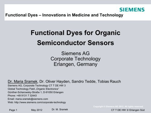
Functional Dyes – Innovations in Medicine and Technology<br />
Functional Dyes for Organic<br />
Semiconductor Sensors<br />
<strong>Siemens</strong> <strong>AG</strong><br />
Corporate Technology<br />
<strong>Erlangen</strong>, Germany<br />
<strong>Dr</strong>. <strong>Maria</strong> <strong>Sramek</strong>, <strong>Dr</strong>. Oliver Hayden, Sandro Tedde, Tobias Rauch<br />
<strong>Siemens</strong> <strong>AG</strong>, Corporate Technology CT T DE HW 3<br />
Global Technology Field „Organic Electronics“<br />
Günther-Scharowsky-Straße 1, D-91050 <strong>Erlangen</strong><br />
Phone: +49 9131 7 32443<br />
Email: maria.sramek@siemens.com<br />
Web: http://www.siemens.com/corporate-technology<br />
Page 1 May 2012 <strong>Dr</strong>. M. <strong>Sramek</strong><br />
Copyright © <strong>Siemens</strong> <strong>AG</strong> 2012. All rights reserved.<br />
CT T DE HW 3/ <strong>Erlangen</strong> Süd
Motivation<br />
R&D Program „System Solutions“<br />
Organic<br />
semiconductor<br />
Nanorods<br />
Quantum dots<br />
nanocrystals<br />
Fullerenes<br />
„Working Nanotechnology“<br />
From Materials to Business Concepts<br />
Carbon<br />
nanotubes<br />
X-ray imaging Industrial sensors In-vitro diagnostics Open innovation<br />
Page 2 May 2012 <strong>Dr</strong>. M. <strong>Sramek</strong><br />
Copyright © <strong>Siemens</strong> <strong>AG</strong> 2012. All rights reserved.<br />
CT T DE HW 3/ <strong>Erlangen</strong> Süd
Outline<br />
1. Introduction<br />
2. Processing<br />
3. Applications for Visible and Infrared Range<br />
Page 3 May 2012 <strong>Dr</strong>. M. <strong>Sramek</strong><br />
Copyright © <strong>Siemens</strong> <strong>AG</strong> 2012. All rights reserved.<br />
CT T DE HW 3/ <strong>Erlangen</strong> Süd
Outline<br />
1. Introduction<br />
1.a - Review<br />
1.b - Organic Photodiodes<br />
2. Processing<br />
3. Applications for Visible and Infrared Range<br />
Page 4 May 2012 <strong>Dr</strong>. M. <strong>Sramek</strong><br />
Copyright © <strong>Siemens</strong> <strong>AG</strong> 2012. All rights reserved.<br />
CT T DE HW 3/ <strong>Erlangen</strong> Süd
„Silicon is Gods Material“ and What About Organics?<br />
Crystalline and impurityfree<br />
substrates<br />
12‘‘/30 cm<br />
Workhorse - wafer<br />
Aim: Integration to cut costs (CMOS paradigm)<br />
Organic electronics – which way to go:<br />
- Low-cost processing vs. efficiency<br />
- Performance vs. material costs/purity<br />
- Large footprint vs. integrated solutions<br />
- Lifetime vs. Flexibility<br />
- Premium vs. low-cost products<br />
Page 5 May 2012 <strong>Dr</strong>. M. <strong>Sramek</strong><br />
Copyright © <strong>Siemens</strong> <strong>AG</strong> 2012. All rights reserved.<br />
CT T DE HW 3/ <strong>Erlangen</strong> Süd<br />
Molecules/Polymers<br />
Roll-to-roll
„Nobel History“ of Conductive Organics<br />
1996<br />
2000<br />
Fullerenes („Buckyballs“) Conductive Polymers<br />
„Replace silicon“ and „organics beyond silicon bandgap limit“<br />
Page 6 May 2012 <strong>Dr</strong>. M. <strong>Sramek</strong><br />
Copyright © <strong>Siemens</strong> <strong>AG</strong> 2012. All rights reserved.<br />
CT T DE HW 3/ <strong>Erlangen</strong> Süd
Properties of Small Molecules & Polymers<br />
Small molecules<br />
Amorphous to highly crystalline, designed for the target application OLED - OFET<br />
High mobility possible<br />
Cheap purification (sublimation, re-crystallization)<br />
Ready for deposition – minor batch dependence<br />
Vacuum deposition<br />
Polymers<br />
Amorphous to crystalline domains, designed for the target application (any)<br />
Low to medium mobility<br />
Expensive purification (chromatography, re-precipitation)<br />
Most are only soluble in chlorinated & aromatic solvents<br />
Specific deposition formulation necessary – major batch dependence<br />
Solution deposition (no vacuum deposition processes)<br />
The performance requirements of the application influences<br />
the choice of materials and the setup of equipment<br />
Page 7 May 2012 <strong>Dr</strong>. M. <strong>Sramek</strong><br />
Copyright © <strong>Siemens</strong> <strong>AG</strong> 2012. All rights reserved.<br />
CT T DE HW 3/ <strong>Erlangen</strong> Süd
Device Fabrication<br />
Silicon Organics<br />
Page 8 May 2012 <strong>Dr</strong>. M. <strong>Sramek</strong><br />
Copyright © <strong>Siemens</strong> <strong>AG</strong> 2012. All rights reserved.<br />
CT T DE HW 3/ <strong>Erlangen</strong> Süd
Revolution to Evolution<br />
Example of OLED Display Developments<br />
Uni Bayreuth<br />
1994<br />
Philips, Passiv Matrix<br />
1999<br />
Sanyo-Kodak 2000<br />
Sony 11-inch OLED<br />
2008<br />
BenQ/<strong>Siemens</strong><br />
Activ Matrix 2006<br />
Page 9 May 2012 <strong>Dr</strong>. M. <strong>Sramek</strong><br />
Copyright © <strong>Siemens</strong> <strong>AG</strong> 2012. All rights reserved.<br />
CT T DE HW 3/ <strong>Erlangen</strong> Süd<br />
Samsung 2009<br />
Mitsubishi 155-inch OLED<br />
2009<br />
The Holy Grail – Flexible TV
Pros and Cons<br />
Pros:<br />
Technology is compatible with Large area processes (low cost)<br />
Low temperature processing (low cost)<br />
Molecules and polymers can be tailored for specific electronic or optical<br />
properties<br />
Compatible with inorganic semiconductors<br />
Cons:<br />
Low carrier mobility<br />
Electronic and optical stability of the materials<br />
Processing is incompatible with classical processing in semiconductor<br />
industry<br />
Page 10 May 2012 <strong>Dr</strong>. M. <strong>Sramek</strong><br />
Copyright © <strong>Siemens</strong> <strong>AG</strong> 2012. All rights reserved.<br />
CT T DE HW 3/ <strong>Erlangen</strong> Süd
Outline<br />
1. Introduction<br />
1.a - Review<br />
1.b - Organic Photodiodes<br />
2. Processing<br />
3. Applications for Visible and Infrared Range<br />
Page 11 May 2012 <strong>Dr</strong>. M. <strong>Sramek</strong><br />
Copyright © <strong>Siemens</strong> <strong>AG</strong> 2012. All rights reserved.<br />
CT T DE HW 3/ <strong>Erlangen</strong> Süd
Organic Diode<br />
Solid state: PN-junction<br />
p-type n-type<br />
Depletion region<br />
Anode Cathode<br />
Organic: „Bulk heterojunction“<br />
Page 12 May 2012 <strong>Dr</strong>. M. <strong>Sramek</strong><br />
Copyright © <strong>Siemens</strong> <strong>AG</strong> 2012. All rights reserved.<br />
CT T DE HW 3/ <strong>Erlangen</strong> Süd<br />
C -<br />
O<br />
OMe<br />
O<br />
OMe<br />
C 3-<br />
C 3-<br />
O 4+<br />
O<br />
OMe<br />
C 4-<br />
C 3-<br />
O<br />
OMe<br />
C-<br />
-<br />
C<br />
Semiconducting polymer<br />
O<br />
OMe<br />
+<br />
C -<br />
O 4+<br />
C -<br />
O<br />
OMe<br />
C 3-<br />
O<br />
OMe<br />
O<br />
OMe<br />
C 2-<br />
C 2-<br />
C 2-<br />
O<br />
OMe<br />
Fullerene<br />
Anode Cathode<br />
Bulk heterojunction = blend of electron donor/acceptor (eg. polythiophene/fullerene)<br />
No distinct pn-junction as in solid-state devices<br />
High absorption coefficient of the semiconducting polymers (~10 5 cm -1 )<br />
O<br />
OMe<br />
C -<br />
C -<br />
C 3-<br />
O<br />
OMe<br />
C 2-<br />
C -<br />
O<br />
OMe
Layer Stack of Organic Photodiodes (OPDs)<br />
ITO (Anode)<br />
Encapsulation<br />
Cathode<br />
Bulk heterojunction (P3HT/PCBM/quantum dots)<br />
Interlayer<br />
Substrate<br />
ITO (Anode)<br />
Page 13 May 2012 <strong>Dr</strong>. M. <strong>Sramek</strong><br />
Copyright © <strong>Siemens</strong> <strong>AG</strong> 2012. All rights reserved.<br />
CT T DE HW 3/ <strong>Erlangen</strong> Süd
EQE (normalized)<br />
VIS to NIR Spectral Sensitivity<br />
1,0<br />
0,8<br />
0,6<br />
0,4<br />
0,2<br />
0,0<br />
Standard P3HT/PCBM<br />
(cf. plastic solar cells)<br />
400 500 600 700 800 900 1000<br />
Wavelength (nm)<br />
Low bandgap absorber<br />
Organic absorber up to ~1 µm<br />
Inorganic absorber >1 µm<br />
400 500 600 700 800 900 1000 1100<br />
Page 14 May 2012 <strong>Dr</strong>. M. <strong>Sramek</strong><br />
Copyright © <strong>Siemens</strong> <strong>AG</strong> 2012. All rights reserved.<br />
CT T DE HW 3/ <strong>Erlangen</strong> Süd<br />
EQE (%)<br />
80<br />
70<br />
60<br />
50<br />
40<br />
30<br />
20<br />
10<br />
0<br />
-10<br />
Wavelength (nm)
Current Density (mA/cm²)<br />
Current/Voltage Characteristics<br />
10 1<br />
10 0<br />
10 -1<br />
10 -2<br />
10 -3<br />
10 -4<br />
10 -5<br />
10 -6<br />
10 -7<br />
10 -8<br />
10 -9<br />
Reverse bias<br />
AM 1.5 (solar)<br />
532 nm @ 780 µW/cm 2<br />
Dark current<br />
-5 -4 -3 -2 -1 0 1 2<br />
Voltage (V)<br />
OPD active area<br />
1 cm²<br />
Statistics over 100 devices<br />
Forward bias<br />
5V.light 1V.light<br />
Page 15 May 2012 <strong>Dr</strong>. M. <strong>Sramek</strong><br />
Copyright © <strong>Siemens</strong> <strong>AG</strong> 2012. All rights reserved.<br />
CT T DE HW 3/ <strong>Erlangen</strong> Süd<br />
Current density (mA/cm 2 )<br />
Current density (mA/cm 2 )<br />
1x10 -4<br />
1x10 -4<br />
8x10 -5<br />
6x10 -5<br />
4x10 -5<br />
2x10 -5<br />
0,35<br />
0,30<br />
0,25<br />
0,20<br />
0,15<br />
0<br />
Dark currents<br />
5V.dark 1V.dark<br />
Photocurrents
Outline<br />
1. Introduction<br />
2. Processing<br />
3. Applications for Visible and Infrared Range<br />
Page 16 May 2012 <strong>Dr</strong>. M. <strong>Sramek</strong><br />
Copyright © <strong>Siemens</strong> <strong>AG</strong> 2012. All rights reserved.<br />
CT T DE HW 3/ <strong>Erlangen</strong> Süd
Coating Techniques Comparison:<br />
Spin coating / Doctor blading / Spray coating<br />
Spin coating<br />
Doctor blading<br />
Spray coating<br />
PEDOT:PSS<br />
Page 17 May 2012 <strong>Dr</strong>. M. <strong>Sramek</strong><br />
Copyright © <strong>Siemens</strong> <strong>AG</strong> 2012. All rights reserved.<br />
CT T DE HW 3/ <strong>Erlangen</strong> Süd
Spray Coating as Fabrication Process for OPDs<br />
OPD fabrication with spray coating<br />
in ambient conditions:<br />
Substrate independence<br />
Adjustable layer thickness<br />
Multiple spray-coated layers<br />
Flexibility using solvents<br />
Layer roughness is not a limitation<br />
Low/high throughput technique<br />
Scalable technology<br />
Movie „Spray coating of OPDs“<br />
S. Tedde et al., Fully Spray Coated Organic Photodiodes,<br />
Nano Letters 9 (3), 980 (2009)<br />
Page 18 May 2012 <strong>Dr</strong>. M. <strong>Sramek</strong><br />
Copyright © <strong>Siemens</strong> <strong>AG</strong> 2012. All rights reserved.<br />
CT T DE HW 3/ <strong>Erlangen</strong> Süd
Outline<br />
1. Introduction<br />
2. Processing<br />
3. Applications for Visible and Infrared Range<br />
Page 19 May 2012 <strong>Dr</strong>. M. <strong>Sramek</strong><br />
Copyright © <strong>Siemens</strong> <strong>AG</strong> 2012. All rights reserved.<br />
CT T DE HW 3/ <strong>Erlangen</strong> Süd
Application in the Visible Range:<br />
Organic Matrix X-Ray Detector<br />
X-Ray image of<br />
hand phantom:<br />
Backplane<br />
Pixels<br />
Processed panel<br />
Page 20 May 2012 <strong>Dr</strong>. M. <strong>Sramek</strong><br />
Copyright © <strong>Siemens</strong> <strong>AG</strong> 2012. All rights reserved.<br />
CT T DE HW 3/ <strong>Erlangen</strong> Süd
Application in the NIR Range:<br />
Small Bandgap Polymer NIR OPDs<br />
– Fabrication Parameters<br />
Substrate size: 50x50 mm²<br />
Number of OPDs on each substrate: 16<br />
Single OPD active area : 71.4 mm²<br />
poly[2,6-(4,4-bis-(2-ethylhexyl)-4H-cyclopenta[2,1-b;3,4-<br />
b]dithiophene)-alt-4,7-(2,1,3-benzothiadiazole)]<br />
(PCPDTBT)<br />
Semiconductor: blend of PCBM / PCPDTBT<br />
PCPDTBT E g : 1.46 eV<br />
Easy and fast<br />
production processes<br />
Large area<br />
(cm² range)<br />
Thin<br />
(< 1mm)<br />
Acknowledgements:<br />
Semitransparent<br />
Page 21 May 2012 <strong>Dr</strong>. M. <strong>Sramek</strong><br />
Copyright © <strong>Siemens</strong> <strong>AG</strong> 2012. All rights reserved.<br />
CT T DE HW 3/ <strong>Erlangen</strong> Süd
Dynamic Response and f -3dB<br />
Signal (20*log(U/U 0 )) [dB]<br />
0<br />
-2<br />
-4<br />
-6<br />
-8<br />
-10<br />
Active area: 0.7 cm 2<br />
Signal [dB]<br />
-3dB<br />
f -3bB = 130 KHz<br />
10 100 1k 10k 100k<br />
Frequency [Hz]<br />
Light source: - 1 KingBright SMD Chip LED KPL-3015SRC-PRV<br />
( peak ~660 nm) super bright red light<br />
- Light intensity ~ 130 µW/cm²<br />
Page 22 May 2012 <strong>Dr</strong>. M. <strong>Sramek</strong><br />
Copyright © <strong>Siemens</strong> <strong>AG</strong> 2012. All rights reserved.<br />
CT T DE HW 3/ <strong>Erlangen</strong> Süd
Application in the NIR Range:<br />
Light Barrier with OPDs<br />
Motivation<br />
Specification<br />
Demonstrate potential of organic photodiodes<br />
for new multidimensional light barrier applications<br />
Show that OPDs can substitute „silicon“ @ NIR<br />
Optic-free light barrier for variable emitter/detector<br />
distance<br />
High flexibility with respect to active area (mm²-cm²)<br />
Quadrant functionality:<br />
- Self-alignment of emitter/detector<br />
- Determination of direction/angle, and speed<br />
Page 23 May 2012 <strong>Dr</strong>. M. <strong>Sramek</strong><br />
Copyright © <strong>Siemens</strong> <strong>AG</strong> 2012. All rights reserved.<br />
CT T DE HW 3/ <strong>Erlangen</strong> Süd
Organic Quadrant Sensor (~4 cm² Active Area)<br />
Resolution Limit ~1 µm<br />
Distance (µm)<br />
1,0<br />
0,0<br />
-1,0<br />
-2,0<br />
-3,0<br />
-4,0<br />
-5,0<br />
-6,0<br />
-7,0<br />
1.5 µm steps @ 15°<br />
X-axis<br />
40 42 44 46 48 50 52 54<br />
Time (s)<br />
Y-axis<br />
4 organic photodiodes (A, B, C, D) giving X/Y positioning results for a light spot<br />
Absolute X/Y position is calculated according to formula<br />
Page 24 May 2012 <strong>Dr</strong>. M. <strong>Sramek</strong><br />
Copyright © <strong>Siemens</strong> <strong>AG</strong> 2012. All rights reserved.<br />
CT T DE HW 3/ <strong>Erlangen</strong> Süd<br />
X<br />
Y<br />
( B D) ( A C)<br />
<br />
A B C D<br />
( A B) ( C D)<br />
<br />
A B C D
Application in the NIR Range:<br />
PSD/Light Barrier @ 660 nm Demonstrator<br />
4 Quadrant OPD Light Barrier<br />
Conveyor belt Implementation<br />
Page 25 May 2012 <strong>Dr</strong>. M. <strong>Sramek</strong><br />
Copyright © <strong>Siemens</strong> <strong>AG</strong> 2012. All rights reserved.<br />
CT T DE HW 3/ <strong>Erlangen</strong> Süd
NIR OPDs with a Small Molecule Absorber:<br />
Squaraine (SQ+PCBM = Polymer-Free BHJ)<br />
EQE [%]<br />
100<br />
80<br />
60<br />
40<br />
20<br />
External quantum efficiency IV-characteristic<br />
EQE 0 V<br />
- 1 V<br />
- 2 V<br />
- 3 V<br />
- 4 V<br />
- 5 V<br />
- 6 V<br />
- 7 V<br />
0<br />
400 600 800 1000<br />
Wavelength [nm]<br />
-5 -4 -3 -2 -1 0 1 2<br />
Voltage [V]<br />
NIR peak sensitivity ~800 nm (tunable); low absorption in visible spectrum<br />
Dynamic response: -3 dB @ ~150 kHz (~1 cm² active area)<br />
Synthesis yield >90% (effortless up-scaling)<br />
Key advantage: Low cost absorber; no extensive polymer purification needed<br />
Page 26 May 2012 <strong>Dr</strong>. M. <strong>Sramek</strong><br />
Copyright © <strong>Siemens</strong> <strong>AG</strong> 2012. All rights reserved.<br />
CT T DE HW 3/ <strong>Erlangen</strong> Süd<br />
Current Density [mA cm -2 ]<br />
10 2<br />
10 1<br />
10 0<br />
10 -1<br />
10 -2<br />
10 -3<br />
10 -4<br />
10 -5<br />
10 -6<br />
532 nm<br />
Solar<br />
870 nm<br />
Dark
Small Molecule Absorber Squaraine:<br />
Dynamic Response and f -3dB<br />
sprayed<br />
doctorbladed<br />
Signal (20*log(U/U 0 )) [dB]<br />
0<br />
-2<br />
-4<br />
-6<br />
Reverse bias: -2V applied<br />
OPD response<br />
f -3dB<br />
f -3dB = 100 KHz<br />
10 100 1k 10k 100k 1M<br />
Frequency [Hz]<br />
Page 27 May 2012 <strong>Dr</strong>. M. <strong>Sramek</strong><br />
Copyright © <strong>Siemens</strong> <strong>AG</strong> 2012. All rights reserved.<br />
CT T DE HW 3/ <strong>Erlangen</strong> Süd
Application in the SWIR Range:<br />
Pushing The Limits of OPDs with Quantum Dots<br />
Visible Application: Photography<br />
Si Bandgap<br />
NIR Imaging (0.7-2.5 µm):<br />
- Active night vision systems<br />
(NIR source)<br />
- Security applications<br />
(machine vision)<br />
- Tomography<br />
(Tissue scanning)<br />
QD range<br />
MIR Imaging (3-5 µm):<br />
- Thermal Imaging<br />
- Passive night vision systems<br />
www.omega.com<br />
Page 28 May 2012 <strong>Dr</strong>. M. <strong>Sramek</strong><br />
Copyright © <strong>Siemens</strong> <strong>AG</strong> 2012. All rights reserved.<br />
CT T DE HW 3/ <strong>Erlangen</strong> Süd
Hybrid Organic/Colloidal Photodiodes<br />
Schematic layout of an a-Si active matrix<br />
TFT panel with OPDs<br />
Photosensitive layer:<br />
Bulk heterojunction (P3HT:PCBM)<br />
with embedded PbS QD absorber<br />
Imager: 256x256 pixels<br />
with 154 µm pixel pitch<br />
T. Rauch et al., Near-infrared imaging with quantum<br />
dot sensitized organic photodiodes, Nature Photonics,<br />
3, 332-336 (2009)<br />
Page 29 May 2012 <strong>Dr</strong>. M. <strong>Sramek</strong><br />
Copyright © <strong>Siemens</strong> <strong>AG</strong> 2012. All rights reserved.<br />
CT T DE HW 3/ <strong>Erlangen</strong> Süd
Tunable Spectral Response with High EQE<br />
EQE of an organic photodiode sensitized with<br />
PbS-QDs of 4.6 nm diameter<br />
Peak sensitivity at 1290 nm with 18.4% EQE<br />
Electrons<br />
EQE<br />
~ (%)<br />
Photon<br />
Tunable NIR sensitivity with increasing QD<br />
diameter<br />
Cut-off wavelength: 1350 nm to 1850 nm<br />
Page 30 May 2012 <strong>Dr</strong>. M. <strong>Sramek</strong><br />
Copyright © <strong>Siemens</strong> <strong>AG</strong> 2012. All rights reserved.<br />
CT T DE HW 3/ <strong>Erlangen</strong> Süd
Current/Voltage Characteristic and Lifetime<br />
I-V characteristics<br />
High photoresponse for polychromatic light<br />
>870 nm<br />
Stable diode rectification ratio<br />
up to 8000 @ +/-2V<br />
Lifetime of more than one year!<br />
Accelerated lifetime conditions of 38°C and<br />
90% rel. Humidity<br />
Stability for both, dark and light currents<br />
in the visibile and NIR region<br />
Page 31 May 2012 <strong>Dr</strong>. M. <strong>Sramek</strong><br />
Copyright © <strong>Siemens</strong> <strong>AG</strong> 2012. All rights reserved.<br />
CT T DE HW 3/ <strong>Erlangen</strong> Süd
Energy Band Diagram<br />
PbS<br />
Staggered band alignment between<br />
P3HT and the PbS QD<br />
Almost flat band condition between the LUMO<br />
of PCBM and energy level of the PbS QD<br />
(first excitonic transition)<br />
QD can act as sensitizer and as<br />
traps<br />
Conduction via QDs is unlikely due<br />
to long oleic acid ligands and the<br />
conductivity is orders of magnitudes<br />
lower compared to the bulkheterojunction<br />
material P3HT/PCBM<br />
No energy barrier for electron<br />
transfer between QD and PCBM;<br />
applied bias assists charge carrier<br />
transfer<br />
Hole transfer might be possible from<br />
QDs to P3HT and/or to PEDOT<br />
Page 32 May 2012 <strong>Dr</strong>. M. <strong>Sramek</strong><br />
Copyright © <strong>Siemens</strong> <strong>AG</strong> 2012. All rights reserved.<br />
CT T DE HW 3/ <strong>Erlangen</strong> Süd
SWIR-Imaging<br />
Images @ 1310 nm Movies @ 1310 nm<br />
Shadow cast of a slide (flat fielding)<br />
Original slide showing a monarch butterlfly<br />
Si works only up to 1100 nm!<br />
256x256 a-Si AM TFT panel (154 µm pixel pitch)<br />
Video shows 2 woodlice (young woodlouse on<br />
the back/adult woodlouse cleans its antennae<br />
with a foreleg)<br />
Page 33 May 2012 <strong>Dr</strong>. M. <strong>Sramek</strong><br />
Copyright © <strong>Siemens</strong> <strong>AG</strong> 2012. All rights reserved.<br />
CT T DE HW 3/ <strong>Erlangen</strong> Süd
Conclusion<br />
Motivation:<br />
Replace silicon @ NIR for large active areas<br />
Solution-processable semiconductors beyond silicon bandgap limit<br />
Industrial fabrication process for OPD<br />
Spray coating<br />
Excellent statistics of IV-characteristics<br />
NIR sensors applying the dominant design of bulk heterojunctions<br />
Tunable absorber (polymer-free system)<br />
Industrial sensor prototypes (multifunctional light-barrier up to 900 nm)<br />
<br />
Low-cost imager for SWIR<br />
Quantum dots as absorber<br />
Imaging and videos >1100 nm with hybrid organic photodiode matrix<br />
Page 34 May 2012 <strong>Dr</strong>. M. <strong>Sramek</strong><br />
Copyright © <strong>Siemens</strong> <strong>AG</strong> 2012. All rights reserved.<br />
CT T DE HW 3/ <strong>Erlangen</strong> Süd
Acknowledgements<br />
<strong>Dr</strong>. Oliver Hayden<br />
Sandro Tedde<br />
Tobias Rauch<br />
Regina Pflaum<br />
<strong>Dr</strong>. Joachim Wecker<br />
Prof. C. Brabec<br />
(ex-Konarka)<br />
Prof. W. Heiss<br />
(Uni Linz)<br />
Prof. Moungi<br />
Bawendi<br />
(MIT)<br />
Thank you for your attention!<br />
Page 35 May 2012 <strong>Dr</strong>. M. <strong>Sramek</strong><br />
Copyright © <strong>Siemens</strong> <strong>AG</strong> 2012. All rights reserved.<br />
CT T DE HW 3/ <strong>Erlangen</strong> Süd
Wishes and Hopes of Organic Electronics …<br />
Organic Electronics<br />
CMOS<br />
Page 36 May 2012 <strong>Dr</strong>. M. <strong>Sramek</strong><br />
Copyright © <strong>Siemens</strong> <strong>AG</strong> 2012. All rights reserved.<br />
CT T DE HW 3/ <strong>Erlangen</strong> Süd