Maria Bayard Dühring - Solid Mechanics
Maria Bayard Dühring - Solid Mechanics
Maria Bayard Dühring - Solid Mechanics

You also want an ePaper? Increase the reach of your titles
YUMPU automatically turns print PDFs into web optimized ePapers that Google loves.
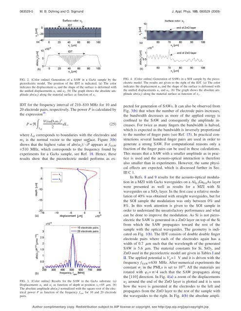
083529-5 M. B. <strong>Dühring</strong> and O. Sigmund J. Appl. Phys. 105, 083529 2009<br />
FIG. 2. Color online Generation of a SAW in a GaAs sample by the<br />
piezoelectric model. The position of the IDT is indicated. a The color<br />
indicates the displacement u 2 and the shape of the surface is deformed with<br />
the unified displacements u 1 and u 2. b The graph shows the absolute amplitude<br />
absu 2 along the material surface as function of x 1<br />
IDT for the frequency interval of 210–810 MHz for 10 and<br />
20 electrode pairs, respectively. The power P is calculated by<br />
the expression 16<br />
P = R Lel<br />
ViD2m2 <br />
dL, 25<br />
2<br />
where L el corresponds to boundaries with the electrodes and<br />
m 2 is the normal vector to the upper surface. Figure 3b<br />
shows that the highest value of absu 2/P appears at f SAW<br />
=510 MHz, which corresponds to the frequency found by<br />
experiments for a GaAs sample, see Ref. 18. Hence, these<br />
results show that the piezoelectric model performs as ex-<br />
(a)<br />
(b)<br />
FIG. 3. Color online Results for the SAW in the GaAs substrate. a<br />
Displacements u 1 and u 2 as function of depth at position x 1=85 m. b<br />
The absolute amplitude absu 2 normalized with the square root of the electrical<br />
power P as function of the frequency f saw for 10 and 20 electrode<br />
pairs.<br />
FIG. 4. Color online Generation of SAWs in a SOI sample by the piezoelectric<br />
model. The results are given to the right of the IDT. a The color<br />
indicates the displacement u 2 and the shape of the surface is deformed with<br />
the unified displacements u 1 and u 2. b The graph shows the absolute amplitude<br />
absu 2 along the material surface as function of x 1.<br />
pected for generation of SAWs. It can also be observed from<br />
Fig. 3b that when the number of electrode pairs increases,<br />
the bandwidth decreases as more of the applied energy is<br />
confined to the SAW and consequently the amplitude increases.<br />
For twice as many fingers the bandwidth is halved,<br />
which is expected as the bandwidth is inversely proportional<br />
to the number of finger pairs see Ref. 15. In practical constructions<br />
several hundred finger pairs are used in order to<br />
generate a strong SAW. For computational reasons only a<br />
fraction of the finger pairs can be used in these calculations.<br />
This means that a SAW with a smaller amplitude as in practice<br />
is used and the acousto-optical interaction is therefore<br />
also smaller than in experiments. However, the same physical<br />
effects are expected, which is discussed further in Sec.<br />
IIIC1.<br />
In Refs. 8 and 9 results for the acousto-optical modulation<br />
in a MZI with GaAs waveguides on a Al 0.2Ga 0.8As layer<br />
were presented as well as results for a MZI with Si<br />
waveguides on a SiO 2 layer. In the first case a relative modulation<br />
of 40% was obtained with straight waveguides, but for<br />
the SOI sample the modulation was only between 0% and<br />
8%. In this work attention is given to the SOI sample in<br />
order to understand the unsatisfactory performance and what<br />
can be done to improve the modulation. As Si is not piezoelectric<br />
the SAW is generated in a ZnO layer on top of the Si<br />
from which the SAW propagates toward the rest of the<br />
sample with the optical waveguides. The geometry is indicated<br />
on Fig. 1b. The IDT consists of double double finger<br />
electrode pairs where each of the electrodes again has a<br />
width of 0.7 m such that the wavelength of the generated<br />
SAW is 5.6 m. The material constants for Si, SiO 2, and<br />
ZnO used in the piezoelectric model are given in Tables I and<br />
II. The applied potential is V p=1 V and it is driven with the<br />
frequency f SAW=630 MHz. After numerical experiments the<br />
constant j in the PMLs is set to 10 10 . All the materials are<br />
rotated with 2=/4 such that the SAW propagates along<br />
the 110 direction. In Fig. 4a a zoom of the displacements<br />
u 2 around the end of the ZnO layer is plotted and it is seen<br />
how the wave is generated at the electrodes to the left and<br />
propagates from the ZnO layer to the rest of the sample with<br />
the waveguides to the right. In Fig. 4b the absolute ampli-<br />
Author complimentary copy. Redistribution subject to AIP license or copyright, see http://jap.aip.org/jap/copyright.jsp