扫描隧道显微镜诱导的发光 - 中国科学院物理研究所
扫描隧道显微镜诱导的发光 - 中国科学院物理研究所
扫描隧道显微镜诱导的发光 - 中国科学院物理研究所

You also want an ePaper? Increase the reach of your titles
YUMPU automatically turns print PDFs into web optimized ePapers that Google loves.
国家自然科学基金委员会<br />
数理学部实验物理讲习班<br />
Introduction to STM induced Luminescence<br />
扫描隧道显微镜诱导发光研究简介<br />
Zhen-Chao Dong (董振超)<br />
University of Science and Technology of China<br />
(中国科学技术大学)<br />
Email: zcdong@ustc.edu.cn<br />
March 29, 2007<br />
e –<br />
+<br />
_<br />
hv
Why?<br />
Definition<br />
Motivation<br />
What?<br />
Outline<br />
国家自然科学基金委员会<br />
数理学部实验物理讲习班<br />
What have been done?<br />
What to do next?<br />
How?<br />
Experimental techniques<br />
Theoretical calculations
1. Brief Introduction to the Background<br />
• Definition<br />
• Motivations<br />
• Luminescence from metal-oxide-metal (MOM) tunnel junctions<br />
• Early studies of photon emission by STM<br />
2. Experimental Techniques<br />
• Photon collection systems<br />
• Photon detection systems<br />
• Modes of measurements<br />
3. Status of STM Induced Luminescence<br />
• Metals<br />
• Semiconductors<br />
• Molecules and Nanostructures<br />
• Theoretical models<br />
4. Summary<br />
Contents<br />
国家自然科学基金委员会<br />
数理学部实验物理讲习班
国家自然科学基金委员会<br />
数理学部实验物理讲习班<br />
1. Brief Introduction<br />
Scanning Tunneling Microscope<br />
(STM) Induced Luminescence:<br />
Definition?<br />
Motivations?<br />
Early History?
Definition: STM Induced Luminescence (STML)<br />
Beyond imaging and manipulation<br />
国家自然科学基金委员会<br />
数理学部实验物理讲习班<br />
e –<br />
+<br />
_<br />
e<br />
hv<br />
I = I elastic + I inelastic<br />
Elastic Tunneling Process:<br />
Conventional STM phenomena<br />
• Topography<br />
• Spectroscopy<br />
e.g., transport: I-V, dI/dV<br />
barrier height: I-s<br />
(Inelastic contributions exist!)<br />
Inelastic Process:<br />
Vibrational excitation: d 2 I/dV 2 (IETS)<br />
Tip-induced plasmon<br />
}<br />
Radiative decay!<br />
Electronic excitation STML or STL<br />
Tunneling electrons:<br />
Highly localized<br />
excitation source for photon emission!<br />
Tunneling electron excited luminescence!
Motivations<br />
Fundamental Interest:<br />
国家自然科学基金委员会<br />
数理学部实验物理讲习班<br />
• Photons offer various channels for probing tunnel junctions (inelastic process)<br />
(intensity, spectra, emission pattern, polarization, decay kinetics)<br />
• Coupling of electrons, excitons, plasmons, and photons in the nano-cavity<br />
• Fluorescence (exciton) decay kinetics & energy transfer at the nanoscale<br />
• Quantum tuning of photonic states for nano-objects in a nano-environment<br />
• Charge transport dynamics at the interface & through nanostructures<br />
• “Color” STM: chemical identification with high spatial resolution<br />
• New quantum phenomena (strong field enhancements and NF excitation)<br />
Practical Interest:<br />
• Interface parameter control for organic electronics (e.g., OLED, η↑)<br />
• Spectral imaging of single defects or impurities in electronic devices<br />
• Radiative decay engineering for bio-molecular (DNA) mapping<br />
• Nanoscale light source for optical spectroscopy and imaging<br />
• Single-molecule electroluminescence and single-photon sources
例子:<br />
I ( V<br />
)<br />
STM具有极高的空间分辨力,但缺乏化学分析能力:根源<br />
国家自然科学基金委员会<br />
数理学部实验物理讲习班<br />
∝<br />
∫<br />
E<br />
E<br />
v<br />
ρ ( r , E ) =<br />
f<br />
f<br />
+ eV<br />
∑<br />
i<br />
v<br />
ρ ( r , E ) dE<br />
v<br />
ψ ( r )<br />
i<br />
2<br />
δ ( E<br />
Atomic Imaging & Manipulation<br />
Si(111)-7x7<br />
z-direction: 0.01 nm<br />
x,y-direction: 0.1 nm<br />
−<br />
E<br />
i<br />
)<br />
单原子操纵<br />
“量子海市蜃楼”<br />
• STM原子分辨率起源:针尖具有类p z 或d z 2电子态、且结间距很小!<br />
• 隧穿事件几乎由费米面上的自由电子决定,而且涉及多种态;<br />
• 隧穿电流涉及样品和探针,是二者电子态密度的卷积。<br />
探针敏感性<br />
成象不确定性 !<br />
IBM<br />
D. Eigler
国家自然科学基金委员会<br />
数理学部实验物理讲习班<br />
提高STM化学分析能力的途径?<br />
与谱学技术相结合!<br />
扫描隧道谱 荧光发射光谱<br />
王兵、裘晓辉等<br />
专题报告
提高STM化学分析能力的途径一:STM + STS<br />
国家自然科学基金委员会<br />
数理学部实验物理讲习班<br />
空间分辨<br />
(X,Y)<br />
扫描隧道谱: 能级结构信息<br />
空间分辨 + “Z”-分辨<br />
(X,Y) + I-z<br />
(X,Y) + I-V<br />
(X,Y) + dI/dV<br />
(X,Y) + d 2 I/dV 2<br />
空间分辨 + 能量分辨<br />
功函数<br />
电子态<br />
特定电子态<br />
特定振动态 }<br />
非弹性隧穿谱<br />
(IETS技术)<br />
“锁相”技术
提高STM化学分析能力的途径二:STM + FS<br />
国家自然科学基金委员会<br />
数理学部实验物理讲习班<br />
e –<br />
h +<br />
STM诱导发光<br />
ET<br />
HT<br />
+<br />
_<br />
hv<br />
e–h<br />
recombination<br />
原子分辨<br />
STM<br />
+<br />
单光子计数<br />
Optical Detectors<br />
空间、能量、时间<br />
高分辨<br />
隧道结<br />
电荷输运、光学跃迁、<br />
能量转化动力学<br />
高分辨<br />
形貌<br />
+<br />
发光光谱<br />
高分辨化学标识<br />
辐射衰变工程(RDE)<br />
纳米元件、生物分子识别?
e –<br />
h +<br />
表征检测工具<br />
国家自然科学基金委员会<br />
数理学部实验物理讲习班<br />
分子尺度调控研究的多功能复合技术<br />
光学技术 扫描探针技术 伏安曲线测量<br />
ET<br />
HT<br />
+<br />
_<br />
e–h<br />
recombination<br />
“三合一”技术<br />
hv<br />
原子分辨<br />
STM<br />
+<br />
单光子计数<br />
Optical Detectors<br />
空间、能量、时间<br />
高分辨<br />
STM诱导发光技术<br />
空间分辨<br />
(X,Y)<br />
“锁相”技术<br />
“二合一”技术<br />
空间分辨 + “Z”-分辨<br />
(X,Y) + “Z”<br />
(X,Y) + I-V<br />
(X,Y) + dI/dV<br />
(X,Y) + d 2 I/dV 2<br />
空间分辨 + 能量分辨
国家自然科学基金委员会<br />
数理学部实验物理讲习班<br />
Microscopy<br />
in the space domain<br />
单分子研究<br />
Single-Molecule Studies<br />
Spectroscopy<br />
in the frequency domain<br />
SNOM: high time resolution (朱星教授)<br />
Fluorescence decay<br />
in the time domain<br />
空间 能量 时间<br />
STML:<br />
imaging and I-V measurements with high spatial resolution<br />
+ spectra & lifetime
国家自然科学基金委员会<br />
数理学部实验物理讲习班<br />
First report of luminescence<br />
excited by tunneling electrons:<br />
When?<br />
Who?<br />
What system?<br />
Early STML studies?
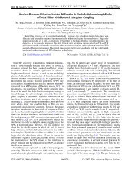
Luminescence from metal-oxide-metal (MOM) tunnel junctions<br />
国家自然科学基金委员会<br />
数理学部实验物理讲习班<br />
J. Lambe and S. L. McCarthy, Phys..Rev. Lett. 37 (923) 1976.<br />
Explanation:<br />
Radiative decay of plasmons!<br />
Inelastic tunneling excitation (IET)<br />
of<br />
optically coupled<br />
surface plasmon modes<br />
V<br />
Emission feature:<br />
hv<br />
Al<br />
Al2O3 Au or Ag<br />
CaF 2<br />
• Broad and continuous;<br />
• Quantum cutoff: hν ≤ eV;<br />
• Bias dependent color:<br />
red (2V) →yellow →blue<br />
• Visible by naked eye<br />
(dark room, η= 10-5 –10-4 )
Related Elementary Excitations: Concepts<br />
国家自然科学基金委员会<br />
数理学部实验物理讲习班<br />
Plasmons(等离激元):<br />
Plasma oscillation― collective motion of the entire electron gas!<br />
Charge density oscillation: the oscillation quantum of charge density wave.<br />
Surface Plasmons(表面等离激元):<br />
Wave-like disturbance of the charge density confined to the surface,<br />
coherent superposition of electron-hole pairs generated by surface excitons<br />
Surface Plaritons(表面极化激元或表面极化声子):<br />
Coupled modes of the surface lattice + electromagnetic field system,<br />
very long wavelength elementary excitation of the surface coupled with the ambient field<br />
Surface Plasmon Plaritons(表面等离极化激元): → Surface Plasmons<br />
Coupled modes of the radiation field and the surface plasmon excitation,<br />
Surface Plasmons + Surface Plaritons (MOM)<br />
表面波的特征 :<br />
电场强度Ez 在界面两侧随距离的增加按指数关系<br />
快速衰减,在 z=0 处极大,故束缚于界面(表<br />
面)上,不能检测到远场光。<br />
A. Zangwill, Physics at Surfaces, 1988.
Oscillating at the plasma frequency<br />
Plasma oscillation,<br />
or, charge density oscillation<br />
Plasmons (等离激元)<br />
国家自然科学基金委员会<br />
数理学部实验物理讲习班<br />
Displacement of the entire electron gas,<br />
as a whole, by a distance d<br />
relative to the fix positive background of ions!<br />
ε(ω) = 1−ω2 p / ω2<br />
ωτ>> 1<br />
Condition for the onset of<br />
propagation of radiation: ω = ω p (ε=0)<br />
If ε>0 (ω>ω p ), E → oscillatory → propagating<br />
If ε
Surface Plasmons(SPs, 表面等离激元)<br />
国家自然科学基金委员会<br />
数理学部实验物理讲习班<br />
Δ•Ε = 0 真空-金属界面处<br />
ε 2 =1<br />
ε 1 = −1 ω s = ω p /√2<br />
ω<br />
ω<br />
ω p<br />
ω<br />
p<br />
1+ ε<br />
p<br />
2<br />
2<br />
ε(ω) = 1-ω2 p / ω2<br />
ω = c ⋅ k<br />
~ k<br />
p<br />
x<br />
ο −1<br />
~ 0.<br />
3 A<br />
0<br />
The dispersion of the SPs<br />
k x<br />
表面等离激元(表面电磁波)<br />
存在的条件:<br />
ε 1 = −|A| ε 2<br />
界面两侧的介电常数异号!<br />
光滑结表面:<br />
k ‖ ≤k r +ω/c<br />
k ‖ >ω/c<br />
波矢(动量)不守恒!不能发光!<br />
粗糙度 破坏平移对称性<br />
波矢匹配!发光!
E F −eV<br />
MOM 隧道结发光机制<br />
国家自然科学基金委员会<br />
数理学部实验物理讲习班<br />
IET<br />
Metal Barrier Metal<br />
隧道结发光是个两步过程:<br />
HED<br />
E F<br />
1、IET electrons excite SPs;<br />
2、SPs couple with the radiation field<br />
→ photon emission!<br />
Optical coupling? → Roughness!<br />
Radiative decay of plasmons!<br />
IET: Inelastic Tunneling<br />
HED: Hot electron decay<br />
Roughness (粗糙度的引入方式):<br />
• Intrinsic sample surface roughness<br />
• Grating structure on the surface<br />
• Prism coupler via ATR<br />
• Nanoparticles on the surface<br />
• Proximity of a sharp tip to the surface<br />
+ Interband transition of semiconductors
国家自然科学基金委员会<br />
数理学部实验物理讲习班<br />
Young et al. (1972)<br />
FE electrons<br />
↓<br />
hν, sec. e− ↓<br />
topography<br />
(NIST)<br />
R. Berndt, Wittenberg 2004<br />
of Junction Luminescence<br />
Lambe & McCarthy (1976)<br />
MOM junction, radiative decay of plasmons, IET<br />
Gimzewski et al. (1988)<br />
Isochromat Spectra<br />
↓<br />
hν, local IPES<br />
(IBM Zurich)
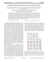
First report on STM induced luminescence!<br />
国家自然科学基金委员会<br />
数理学部实验物理讲习班<br />
Photon-emission Experiments with the Scanning Tunneling Microscope<br />
J. K. Gimzewski, B. Reihl, J. H. Coombs and R. R. Schlittler<br />
IBM Research Division, Zurich Research Laboratory<br />
Z. Phys. B72 (1988) 497; J. Microscopy-Oxford 152 (1988) 325.<br />
Sample<br />
STM tip<br />
Detector<br />
Sample:<br />
Polycrystalline Ta, Si(111); Ag films<br />
Mode of measurements:<br />
Isochromatic spectra with photon energies at 9.5 eV<br />
Results:<br />
Spectra reveal electronic structure information<br />
comparable to inverse photoemission spectroscopy!<br />
Since 1988, extensive research on the surfaces of<br />
metals, semiconductors, and adsorbed molecules has been going on!<br />
Europe, Japan, USA… (30-40 groups)
2. Experimental Techniques<br />
国家自然科学基金委员会<br />
数理学部实验物理讲习班<br />
• Photon collection<br />
• Photon detection<br />
• Modes of measurements<br />
Why limited number of research groups<br />
around the world on STML?<br />
Bias<br />
Adsorbate<br />
Reference<br />
current<br />
Tip<br />
Spectroscopy<br />
Radiated<br />
power<br />
Sample<br />
Spectrometer<br />
S. Ushioda
国家自然科学基金委员会<br />
数理学部实验物理讲习班<br />
STM-Induced Light Emission<br />
Requiring:<br />
good well-defined sample<br />
‘good’ tip!<br />
efficient light collector<br />
highly sensitive photon detector<br />
Success!
国家自然科学基金委员会<br />
数理学部实验物理讲习班<br />
Light Collection System<br />
Target: to achieve a large solid angle coverage<br />
Three types according to optical parts:<br />
Mirror system: Ellipsoidal/parabolic<br />
Fiber system<br />
Lens system<br />
Two types according to collection modes:<br />
Far field collection<br />
Near field collection
UHV Photon STM: Ellipsoidal Mirror Design<br />
国家自然科学基金委员会<br />
数理学部实验物理讲习班<br />
Advantage:<br />
Large solid angle coverage; 48-61%<br />
Free of chromatic aberration<br />
Disadvantage:<br />
Difficult to make and use;<br />
Difficult to align and focus<br />
R. Berndt, R. R. Schlittler, J.K. Gimzewski, J. Vac. Sci. Technolog. B9 (1991) 573. (IBM Zurich)<br />
Y. Suzuki, H. Minoda, N. Yamamoto, Surf. Sci. 438 (1999) 297. (TIT, Japan)
Advantage:<br />
Eclipsing of luminescence by STM<br />
largely minimized →<br />
UHV Photon STM: Parabolic Mirror Design<br />
国家自然科学基金委员会<br />
数理学部实验物理讲习班<br />
M. J. Romero, et al., Nanolett. released 2006-11-24<br />
(Natl Renewable Energy Lab, USA)<br />
High collection efficiency: >10%<br />
1. N. Nilius, et al., Prog. Surf. Sci. 67 (2001)<br />
99; Chem. Phys. Lett. 413 (2005) 10.<br />
2. S. Egusa, et al., Appl. Phys. Lett.<br />
84 (2004) 1257.<br />
Disadvantage:<br />
Difficult to make, align and focus
UHV Photon STM: Fiber Bundle Design<br />
国家自然科学基金委员会<br />
数理学部实验物理讲习班<br />
Single Fiber (Tohoku Univ)<br />
Φ=600μm, d=1mm, NA=0.2 →<br />
Solid angle coverage: 0.13 sr,<br />
Hemisphere collection efficiency: 2%<br />
T. Tsuruoka and S. Ushioda,<br />
J. Elec. Micr. 53 (2004) 169.<br />
Four Fiber-bundles (NIMS)<br />
M. Sakurai, C. Thirstrup, and M. Aono,<br />
Applied Physics A 80 (2005) 1153. (~5%)<br />
Reasonable collection efficiency,<br />
but relatively difficult to align.
Fiber Tip Design―Near Field Collection Mode<br />
国家自然科学基金委员会<br />
数理学部实验物理讲习班<br />
D. Fujita, et al. (NIMS),<br />
Micr. Res. Techn. 64(2004)403.<br />
T. Murashita (NTT)<br />
J. Vac. Sci. Technol. B 15(1997)32.<br />
Est: 100-fold better than lens system?<br />
Collection efficiency: ~10%<br />
The fiber tip is difficult to<br />
make. Expensive!<br />
Good coupling difficult!
UHV Photon STM: Double Lens Design<br />
国家自然科学基金委员会<br />
数理学部实验物理讲习班<br />
Hemisphere collection efficiency: ~9%<br />
G. Hoffmann, J. Kroger, R. Berndt (Univ. Kiel)<br />
Rev. Sci. Inst. 73 (2002) 305.<br />
Reasonable<br />
collection efficiency<br />
(2−15%)<br />
+<br />
Relatively easy<br />
To align<br />
Light collection systems<br />
used most often<br />
in the STML community!
UHV Photon STM: Photon Detection Systems<br />
国家自然科学基金委员会<br />
数理学部实验物理讲习班<br />
Photon signals emitted from the STM tunnel junction is very weak!<br />
• Inelastic Tunneling (IET) Process: Small excitation efficiency<br />
• Nanoscale junction: Small excitation and emission area<br />
• Emission (angular) over hemi-sphere: Low collection efficiency<br />
Required conditions for photon detectors:<br />
• High sensitivity<br />
• Low dark counts (noise)<br />
Distinguish the signal above the noise!<br />
High S/N ratio!<br />
Ordinary photon detectors operating in the linear mode fail.<br />
X<br />
e.g., non-avalanche photodiode: the photon/electron ratio is one to one.<br />
Multiplier/Gain<br />
or<br />
Integration over Pixels<br />
Single Photon Counting?<br />
tip<br />
-<br />
+ e
Single Photon Counting Techniques<br />
国家自然科学基金委员会<br />
数理学部实验物理讲习班<br />
Three Technologies:<br />
• Silicon Avalanche Photodiode (APD) 雪崩光电二极管<br />
Single Photon Counting Modules (SPCMs),<br />
1 photon → many electrons after avalanche effect, Gain = 1―1000<br />
high quantum efficiency (500-1100 nm, up to 70% at 650 nm), visible-infrared<br />
• Photomultiplier Tubes (PMT) & MCP-PMT 光电倍增管<br />
• Charge Coupled Devices (CCD) 电荷耦合器件<br />
Factors:<br />
• Wavelength<br />
• Sample size<br />
• Speed<br />
• Cost<br />
PerkinElmer-APD: Φ=200 μm, point-like nanoscale sample (focusing not good for large)<br />
fast response (count a photon every 50ns), low dark counts (Peltier cooled, 50 cps)<br />
photon → photocathode (photovoltaic effect) → many electrons, Gain = 105―106 115-900 nm, most sensitive for UV and blue (20%); low dark counts (3-50 cps)<br />
several mm – cm in size, wide range of sample size;<br />
very fast response (30ns), MCP-PMT (TTS=25ps + electronic shutter)<br />
An array of ordinary (non-avalanche) photodiodes, the amount of charge on capacitor<br />
300-1000 nm, up to 90% for LN2-cooled BCCD<br />
CCD pixel: 7μm, but array in mm; very wide range of sample size<br />
low dark count and noise, high SN ratio, but slow.
国家自然科学基金委员会<br />
数理学部实验物理讲习班<br />
Data acquisition / Modes of Measurements<br />
Emission intensity<br />
STM-Induced Light Emission<br />
Bias and current dependency −Threshold, QE(η), excitation nature<br />
Photon maps −Threshold, quantum efficiency, spectral imaging map<br />
Isochromat spectra −Nature of particular emission feature, e.g, IET vs HET<br />
Angular distribution −Polarization effects, dipolar coupling<br />
Optical emission spectra<br />
λ-resolved luminescent spectra −Nature of opt. transition, interaction, ET…<br />
Bias dependence −Threshold, excitation behavior, excitation map<br />
Site dependency −Chemical mapping, spectral imaging map<br />
Time-resolved spectroscopy and photon statistics<br />
Lifetime −Nature of optical transitions and excited states; exciton decay kinetics<br />
Bunching vs antibunching −Photon emission statistics
Examples:<br />
Photon Map & Spectral Imaging Map<br />
国家自然科学基金委员会<br />
数理学部实验物理讲习班<br />
G. Hoffmann, J. Kroger, R. Berndt<br />
Rev. Sci. Inst. 73 (2002) 305.<br />
topograph spectral imaging map<br />
Ag(111) at -3V, 5nA, 100ms/pixel<br />
10 5 cps at 5 nA →η= ~10 -4
国家自然科学基金委员会<br />
数理学部实验物理讲习班<br />
Excitation Spectroscopy<br />
― Excitation Map<br />
G. Hoffmann, J. Kroger, R. Berndt<br />
Rev. Sci. Inst. 73 (2002) 305.<br />
Ag(111)<br />
V t=1.8−9.5 V, I t= 5 nA
Isochromat spectra<br />
国家自然科学基金委员会<br />
数理学部实验物理讲习班<br />
―A support to the IET excitation mechanism<br />
Photon intensity ― Bias voltage<br />
at fixed current (It=5nA) & photon energy ( 2.1 eV, optical bandpass filter)<br />
Example: Cu(111) in the Proximity Field Emission Regime<br />
Resonance state<br />
Vn:<br />
Resonance-state energy<br />
Ep:<br />
Tip-induced-mode energy<br />
• Oscillation of dI/dV ↔ electron standing wave in the tip-sample gap (interference)<br />
• Isochromat spectra: Similar oscillatory behavior but with a constant offset of 2.2 eV!<br />
Field emission resonance states confined in the gap region<br />
Interaction of electrons with tip-induced modes occurs within the tunneling gap!<br />
Inelastic energy loss occurs within the gap → IET excitation mechanism!<br />
Berndt & Gimzewski<br />
Ann. Phys. 2(1993)133
Isochromat spectra<br />
―The “Universal” Intensity Maximum Issue<br />
国家自然科学基金委员会<br />
数理学部实验物理讲习班<br />
Photon intensity ― Bias voltage<br />
at fixed current (It=5nA) & photon energy ( 2.1 eV, optical bandpass filter)<br />
Example: Cu(111) in the Proximity Field Emission Regime<br />
“Universal” intensity maximum at V ~ 3.7 V!<br />
In the tunneling regime: universal intensity maxima at Vb ~ 3 – 4 V,<br />
Independent of tip & sample material, wavelength of detected photons!<br />
Model: Competition of two counteracting mechanisms―<br />
Berndt & Gimzewski<br />
Ann. Phys. 2(1993)133<br />
Johansson, Monreal, Apell, PRB 42(1990)9210.<br />
1. Initial increase: growing number of energetically allowed channels;<br />
2. Drop above ~3.5 V: s-V relation! vertical tip retraction much stronger for 3.5−4V!<br />
→ Smaller field enhancement → Decrease in intensity!
3. Status of STM Induced Luminescence<br />
国家自然科学基金委员会<br />
数理学部实验物理讲习班<br />
• Metals<br />
• Semiconductors<br />
• Molecules and Nanostructures<br />
• Theoretical models and calculations<br />
R. Berndt, Wittenberg 2004
国家自然科学基金委员会<br />
数理学部实验物理讲习班<br />
Young et al. (1972)<br />
FE electrons<br />
↓<br />
hν, sec. e− ↓<br />
topography<br />
(NIST)<br />
R. Berndt, Wittenberg 2004<br />
of Junction Luminescence<br />
Lambe & McCarthy (1976)<br />
MOM junction, radiative decay of plasmons, IET<br />
Gimzewski et al. (1988)<br />
Isochromat Spectra: Ta, Ag<br />
↓<br />
hν, local IPES<br />
(IBM Zurich)
Photon Emission from Metal Surfaces by STM<br />
国家自然科学基金委员会<br />
数理学部实验物理讲习班<br />
R. Berndt, J. K. Gimzewski, P. Johansson, PRL 67(3796)1991<br />
Field emission regime Tunneling regime<br />
Photon emission<br />
dramatically enhanced!<br />
Strikingly different<br />
spectra:<br />
greatly red-shifted!
国家自然科学基金委员会<br />
数理学部实验物理讲习班<br />
Extent: ~5 nm<br />
TIP: coupled, localized plasmons of both sample and tip!<br />
Symmetric/antisymmetric charge density oscillation<br />
Lowest-order mode―dipolar plasmon resonance<br />
Field enhancement G(ε) → Im(ε),damping<br />
η~10 -4 , IET vs HED<br />
Quantum cutoff: hν ≤eV
数理学部实验物理讲习班<br />
photon<br />
experiment theory<br />
Physical Review Letter 74(102) 1995<br />
First report atomic resolution<br />
in STM-induced photon emission!<br />
height 国家自然科学基金委员会
国家自然科学基金委员会<br />
数理学部实验物理讲习班<br />
Uehara, Fujita, Ushioda, PRL 83(1999)2445; Uehara & Ushioda, PRB 66(2002)165420<br />
Recombination of d-band holes with sp electrons + LSP<br />
?
国家自然科学基金委员会<br />
数理学部实验物理讲习班<br />
Phys. Rev. Lett. 93 (2004) 076102<br />
a: Au(110) topograph, b & c: photon map<br />
I: on top, II: below a step, III: in-between<br />
“No variation in spectral shape,<br />
except for a minute, rigid shift.”<br />
PRL 83(1999)2445
国家自然科学基金委员会<br />
数理学部实验物理讲习班<br />
Photon Emission from<br />
Semiconductor Surfaces
Nanometer resolution in luminescence microscopy of III-V heterostructures<br />
国家自然科学基金委员会<br />
数理学部实验物理讲习班<br />
D. L. Abraham, A. Veider, Ch. Schönenberger, H. P. Meier, D. J. Arent, and S. F. Alvarado<br />
First report: IBM Zurich: Appl. Phys. Lett. 56(1564)1990; JVSTB 9(1991)409<br />
Photon Map<br />
GaAs/Al x Ga 1-x As<br />
Quantum well/barrier heterstructures<br />
Renaud & Alvarado: Phys. Rev. B 44(1991)6340.<br />
Mechanism: p-type GaAs<br />
Conventional band edge luminescence:<br />
Electron-hole pair recombination<br />
between CV and VB (E g )!
Injection luminescence from CdS(1120) studied with scanning tunneling microscopy<br />
国家自然科学基金委员会<br />
数理学部实验物理讲习班<br />
R. Berndt, et al., Physical Review B 45 (14095) 1992<br />
G: band-edge emission<br />
C: emission from deep levels<br />
Mechanism:<br />
-V: e-h pair recombination<br />
+V: impact ionization
国家自然科学基金委员会<br />
数理学部实验物理讲习班<br />
A. Downes & M.E. Welland, Phys. Rev. Lett. 81 (1998) 1857<br />
Si(111)-7x7, 3.4 V, 30 nA<br />
Mechanism: Radiative decay of TIP modes!<br />
Lateral:<br />
Vertical:<br />
Plasmon wave function:<br />
Resolution of photon map:<br />
Lateral extent of plasmon modes<br />
~2 nm for R=3 nm and s=0.6 nm
国家自然科学基金委员会<br />
数理学部实验物理讲习班<br />
C.Thirstrup, M. sakurai, K. Stokbro, M. Aono, Phy. Rev. Lett. 82 (1999) 1241<br />
Si(100)-3x1-H (-3 V, 8 nA)<br />
Spatially indirect dipole transition<br />
Between tip (DOS) and sample (DBs) ?
国家自然科学基金委员会<br />
数理学部实验物理讲习班<br />
Photon Emission from<br />
Molecules and Nanostructures<br />
• 0D-Quantum dots<br />
• 1D-Quantum chains<br />
• 2D-Quantum wells<br />
• Organic molecules
国家自然科学基金委员会<br />
数理学部实验物理讲习班<br />
Emission mechanism:<br />
the (1,0) mode of the Mie resonance in Ag nanoclusters<br />
Quantum size effect<br />
Size dependence of the Mie resonance (plasmons)!<br />
vs. shape transition?
国家自然科学基金委员会<br />
数理学部实验物理讲习班<br />
Quantum confinement effect!<br />
MBE<br />
InAs QDs<br />
20-30 nm<br />
Photon Map
国家自然科学基金委员会<br />
数理学部实验物理讲习班<br />
IET emission (TIP) Isochromat spectra<br />
hν=1.63 eV → = offset!<br />
LDOS of 1D-chain resonance states No direct interband transition from Ag chains!
国家自然科学基金委员会<br />
数理学部实验物理讲习班<br />
No direct “interband” transition<br />
from 1D-Ag quantum chains on metal surfaces!<br />
How about<br />
2D-quantum wells on metal surfaces?
Luminescence from Metallic Quantum Wells in a Scanning Tunneling Microscope<br />
国家自然科学基金委员会<br />
数理学部实验物理讲习班<br />
Germar Hoffmann,* Jörg Kliewer, and Richard Berndt<br />
Physical Review Letter 87(176803) 2001
Luminescence from Metallic Quantum Wells in a Scanning Tunneling Microscope<br />
国家自然科学基金委员会<br />
数理学部实验物理讲习班<br />
Germar Hoffmann,* Jörg Kliewer, and Richard Berndt<br />
Physical Review Letter 87(176803) 2001<br />
3<br />
2<br />
1<br />
3<br />
2<br />
1<br />
q<br />
p<br />
p: plasmon<br />
modes<br />
q: quantum<br />
well state<br />
带间跃迁:<br />
OK!
国家自然科学基金委员会<br />
数理学部实验物理讲习班<br />
STM Induced Luminescence from Molecules?<br />
hv<br />
tip<br />
-<br />
+ e-<br />
Excitation source: Highly localized tunneling electrons<br />
Single molecules DIRECTLY adsorbed on the metal surface<br />
Molecule based fluorescence from tunnel junctions?<br />
hv<br />
Feasibility?
Absorbance energy<br />
Light Absorption and Fluorescence<br />
国家自然科学基金委员会<br />
数理学部实验物理讲习班<br />
Absorption=10 -15 s<br />
Fluorescence =10 -9 s<br />
Ground State<br />
Electrons<br />
S 2 excited state<br />
S 1 excited state<br />
Nonradiative<br />
dissipation<br />
Basics of molecular photophysics<br />
光致发光<br />
LUMO<br />
HOMO<br />
π*<br />
π
Organic Electroluminescence (EL)<br />
国家自然科学基金委员会<br />
数理学部实验物理讲习班<br />
E F<br />
注入式电致发光<br />
OLED (Thin Film)<br />
+<br />
h +<br />
LUMO<br />
HOMO<br />
LUMO<br />
HOMO<br />
exciton decay<br />
-<br />
e -<br />
ITO HTL EL ETL Mg<br />
Excitation of Electroluminescence:<br />
• Intrinsic EL: Field/impact excitation (>106 V/cm)<br />
• Injection EL: Excitation by the potential energy<br />
of opposite charge carriers (∼106 V/cm)<br />
Charge carrier: Injection, transport? Spin statistics?<br />
Excition: formation and decay?<br />
E F<br />
电致发光
国家自然科学基金委员会<br />
数理学部实验物理讲习班<br />
Photon Map<br />
C60 on Au(110)
STM induced molecular luminescence<br />
• 1993, Spatially resolved photon map of molecules<br />
C60/Au(110)<br />
——R. Berndt, R. Gaisch, J. K. Gimzewski, et al.,<br />
•••<br />
•••<br />
Science 262 (1993) 1425.<br />
No optical emission spectra!<br />
Nature of emission remains unclear.<br />
• 2002,Spectrally resolved photon maps;<br />
HBDC/Cu(111);<br />
Spacer! Submolecular resolution!<br />
—— Hoffmann, Libioulle and Berndt,<br />
Phys. Rev. B 65 (2002) 212107.<br />
Role of molecules?<br />
Spacer or direct emitter?<br />
国家自然科学基金委员会<br />
数理学部实验物理讲习班<br />
IBM’s need<br />
for sharper display!
国家自然科学基金委员会<br />
数理学部实验物理讲习班<br />
Photon Emission from HBDC on Cu(111) with submolecular resolution<br />
G. Hoffman, L. Libioulle, R. Berndt, Phys. Rev. B65 (2002) 212107<br />
• Spectra: Blue-shifted<br />
• Fluorescence: quenched!<br />
• Role of molecules: “Spacer”!
Photon emission from monolayered porphyrins on Cu(100)<br />
国家自然科学基金委员会<br />
数理学部实验物理讲习班<br />
H2TBPP Porphyrin<br />
H<br />
H<br />
H<br />
H<br />
H H<br />
H H<br />
NH<br />
N<br />
H<br />
H<br />
N<br />
HN<br />
H<br />
H<br />
H<br />
H<br />
H<br />
H<br />
Z.-C. Dong, et al., Surf. Sci. 532 (2003) 237<br />
STL Intensity (cps/nA)<br />
1.5<br />
1.0<br />
0.5<br />
0.0<br />
ML-H2TBPP/Au(100), -2.9 V, 0.1 nA<br />
Au(100), -3.0 V, 10 nA<br />
Theory, 3 V, R = 50 nm, d = 0.4 nm<br />
Blue-shift<br />
400 450 500 550 600 650 700 750 800<br />
Wavelength Sample Bias (nm) (V)<br />
ω 1 ∝ω p (d/8R) 1/4<br />
Monolayer case: Role of molecules: Spacer!
国家自然科学基金委员会<br />
数理学部实验物理讲习班<br />
Photon Emission from Organic Molecules?<br />
Plasmon mediated emission<br />
+<br />
Molecular fluorescence<br />
Coupled / mixed! Fluorescence quenching!<br />
Complication!<br />
Role of molecules?<br />
Spacer or direct emitter?<br />
Evidence to look for: Distinct molecular-specific signals!
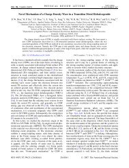
分子荧光复杂性根源: Nonradiative Energy Transfer near Metal Surfaces<br />
国家自然科学基金委员会<br />
数理学部实验物理讲习班<br />
Fluorescence Quenching<br />
or, dipole quenching<br />
Nonradiative damping<br />
ε 0<br />
Molecule<br />
ε<br />
Metal 1<br />
Substrate<br />
Dipole<br />
d<br />
Dipole<br />
Image<br />
dipole<br />
Classical electromagnetic theory:<br />
For large distances, the surface acting as a mirror<br />
to cause electric field interference,<br />
the luminescent lifetime oscillates as a function of d.<br />
τ<br />
0 250 500<br />
d (nm)<br />
For small distances (
Strategy to generate molecular fluorescence<br />
国家自然科学基金委员会<br />
数理学部实验物理讲习班<br />
Decoupling & nanoprobe excitation<br />
_<br />
Nanoprobe<br />
Strong field enhancement at the tip apex<br />
Emissive layer<br />
Decoupling layer<br />
Substrate<br />
Motivation: to avoid fluorescence quenching…
Vibrationally resolved fluorescence excited with submolecular precision<br />
国家自然科学基金委员会<br />
数理学部实验物理讲习班<br />
X. H. Qiu, G. V. Nazin, W. Ho: Science, 299 (2003) 542<br />
ZnEtioI/Al 2O 3/NiAl(110)<br />
Use of an oxide spacer!
Vibrationally resolved fluorescence excited with submolecular precision<br />
国家自然科学基金委员会<br />
数理学部实验物理讲习班<br />
X. H. Qiu, G. V. Nazin, W. Ho: Science, 299 (2003) 542<br />
LUMO+1 → LUMO!<br />
Anionic fluorescence!
国家自然科学基金委员会<br />
数理学部实验物理讲习班<br />
X. H. Qiu, G. V. Nazin, W. Ho: Science, 299 (2003) 542<br />
LUMO+1 → LUMO!<br />
Anionic fluorescence!<br />
?<br />
Can we generate by STM<br />
conventional fluorescence<br />
from neutral molecules<br />
due to<br />
LUMO → HOMO transition?
国家自然科学基金委员会<br />
数理学部实验物理讲习班<br />
Distinct fluorescent peak: Molecular specific!<br />
Clear molecular origin!
国家自然科学基金委员会<br />
数理学部实验物理讲习班<br />
• Bipolar operation ! →<br />
Electrons injected into LUMO at +/- bias!<br />
• Double-barrier junction model!<br />
• Two processes:<br />
LSP + Molecular Fluorescence<br />
• Anomalous upconversion EL:<br />
Hot- electron excitation +<br />
Franck-Condon radiative decay<br />
hν > eV !!! Why? Z.-C. Dong, et al. PRL 92 (2004) 086801.
Decoupling and Charge Carrier Confinement: pn-type Heterostructuring<br />
国家自然科学基金委员会<br />
数理学部实验物理讲习班<br />
Photoluminescence (a.u.)<br />
5000<br />
4000<br />
3000<br />
2000<br />
1000<br />
PL, ex 442 nm, He-Cd laser<br />
STML, +25 V, 2 nA<br />
658<br />
0<br />
0<br />
400 450 500 550 600 650 700 750 800<br />
Wavelength (nm)<br />
723<br />
H 2TBPP<br />
TPD<br />
Cu(100)<br />
250<br />
200<br />
150<br />
100<br />
50<br />
STM Luminescence (a.u.)<br />
-<br />
+<br />
+<br />
e −<br />
Substrate surface<br />
Tip<br />
Dong, et al.: PRL 92, 086801(2004); APL 84, 969(2004); PRB 70, 233204(2004); SRL 13(2006)143.<br />
-<br />
+
国家自然科学基金委员会<br />
数理学部实验物理讲习班<br />
C 60 /NaCl/Au(111)
国家自然科学基金委员会<br />
数理学部实验物理讲习班<br />
STM Photon Emission<br />
Model and Theory?
E F<br />
E F<br />
hv<br />
hv<br />
E F<br />
surface<br />
states<br />
E F<br />
Models?<br />
国家自然科学基金委员会<br />
数理学部实验物理讲习班<br />
Tip-induced-plasmon (TIP) Electron-hole recombination<br />
Metals Semiconductors (direct Eg )<br />
Tip Sample<br />
E F<br />
E F<br />
hv<br />
EC EF EV hv<br />
LUMO<br />
HOMO<br />
Tip Sample<br />
Spatially indirect dipole transition Intramolecular radiative transition<br />
Semiconductors (indirect Eg )<br />
Molecules<br />
E F
Questions?<br />
国家自然科学基金委员会<br />
数理学部实验物理讲习班<br />
Which part, electrons or photons, influences<br />
the light emission spectrum most?<br />
Depends on the system!<br />
• Metals: photons (plasmons)<br />
• Semiconductors: electrons (bandgap, etc.)<br />
• Quantum wells: both<br />
• Molecules: < 1ML, photons; decoupled: both?
国家自然科学基金委员会<br />
数理学部实验物理讲习班<br />
Theoretical Models<br />
Radiation Field Electrons<br />
H = H el-n + H L + H s<br />
H s ↔ A•p<br />
P. Johansson
2 3<br />
o<br />
G ( θ, r ′ , ω)<br />
Local field enhancement<br />
(Boundary charge method)<br />
Radiated power<br />
国家自然科学基金委员会<br />
数理学部实验物理讲习班<br />
2 2<br />
d P ω<br />
2<br />
3<br />
= ∑ d r′ G ( θ, ′ , ω) ⋅ jif<br />
( ′ , ω ) ⋅δ<br />
( Ei− E f − ω)<br />
dΩd( ω) 4π<br />
ε c ∫ r r<br />
h<br />
h<br />
i,<br />
f<br />
z<br />
G z jif<br />
P. Johansson et al., PRB 42, 9210 (1990)<br />
d<br />
ε tip<br />
b<br />
ε sample<br />
j<br />
φ<br />
θ<br />
hω<br />
hω<br />
j ( r ′ , ω )<br />
if<br />
Current density<br />
(Tersoff & Hamann extended)<br />
e<br />
V b<br />
hω<br />
Tip induced plasmon (TIP) modes for a metal tip on a metal surface<br />
P. Johansson et al., PRB 42, 9210 (1990)<br />
J. Aizpurua et al., PRL 89, 156803 (2002)
国家自然科学基金委员会<br />
数理学部实验物理讲习班<br />
G = G(ε, R, d), sensitive to the tip status!<br />
Molecules: No theory for STML yet!<br />
P. Johansson et al., PRB 42, 9210 (1990)<br />
J. Aizpurua et al., PRL 89, 156803 (2002)
国家自然科学基金委员会<br />
数理学部实验物理讲习班<br />
Summary<br />
• STM induced luminescence (STML):<br />
-Photon emission out of inelastic tunneling processes!<br />
(高度局域化隧穿电子 → 非弹性隧穿 → 光子发射!)<br />
-Various information on the nature of tunnel junctions and transitions<br />
-Good tool for studying optoelectronic behavior of single molecules<br />
• Factors affecting STML:<br />
-Geometrical: R, d, ε! (几何因素)<br />
Elastic tunneling current is also important: I t ↔ d ↔ TIP ↔ IET!<br />
-Electronic: Initial and final DOS! (电子结构因素)<br />
Energy level matching (DOS of resonance states/hybrid states)<br />
• Status of the STML research:<br />
-Metals and semiconductors: relatively mature;<br />
-Molecules: many unsolved issues! active and exciting!<br />
e –<br />
in the space, energy, and time domains (单分子光电行为)<br />
(molecular scale electronics and optoelectronics)<br />
+<br />
_<br />
hv
Perspectives:<br />
• Role of molecules?<br />
• Role of substrates (plasmons)?<br />
• Coupling among electron, exciton, plasmon, phonon, photon?<br />
• Raising quantum efficiency (OLED)? Light sources for imaging?<br />
• Single molecule electroluminescence? Single photon sources?<br />
• Lifetime measurements? Luminescence decay kinetics?<br />
• Fluorescence IETS? Chemical mapping?<br />
• Spin injection STML? Spin decay kinetics (population)?<br />
Near-field detection<br />
国家自然科学基金委员会<br />
数理学部实验物理讲习班<br />
Coupled<br />
system!<br />
Far-field detection<br />
• Quantum tuning of photonic states for molecular optoelectronics?<br />
Molecule<br />
Tip<br />
Fiber<br />
-<br />
+<br />
Substrate<br />
Dipolar<br />
radiation
国家自然科学基金委员会<br />
数理学部实验物理讲习班<br />
Thank you !