AR-122E/AR-152E/AR-153E/AR-157E Service-Manual GB
AR-122E/AR-152E/AR-153E/AR-157E Service-Manual GB
AR-122E/AR-152E/AR-153E/AR-157E Service-Manual GB

You also want an ePaper? Increase the reach of your titles
YUMPU automatically turns print PDFs into web optimized ePapers that Google loves.
(<strong>AR</strong>-<strong>157E</strong>)<br />
SERVICE MANUAL<br />
CONTENTS<br />
Parts marked with “ ” are important for maintaining the safety of the machine. Be sure to replace these parts<br />
with the replacement parts specified to maintain the safety and performance of the machine.<br />
SH<strong>AR</strong>P CORPORATION<br />
CODE : 00Z<strong>AR</strong><strong>157E</strong>/A1E<br />
DIGITAL LASER COPIER/<br />
PRINTER<br />
<strong>AR</strong>-<strong>122E</strong><br />
<strong>AR</strong>-<strong>152E</strong><br />
<strong>AR</strong>-<strong>153E</strong><br />
MODEL <strong>AR</strong>-<strong>157E</strong><br />
[ 1 ] GENERAL . . . . . . . . . . . . . . . . . . . . . . . . . . . . . . . . . . . . . . . . . . . 1 - 1<br />
[ 2 ] SPECIFICATIONS. . . . . . . . . . . . . . . . . . . . . . . . . . . . . . . . . . . . . 2 - 1<br />
[ 3 ] CONSUMABLE P<strong>AR</strong>TS. . . . . . . . . . . . . . . . . . . . . . . . . . . . . . . . . 3 - 1<br />
[ 4 ] EXTERNAL VIEWS AND INTERNAL STRUCTURES . . . . . . . . . 4 - 1<br />
[ 5 ] UNPACKING AND INSTALLATION . . . . . . . . . . . . . . . . . . . . . . . 5 - 1<br />
[ 6 ] COPY PROCESS . . . . . . . . . . . . . . . . . . . . . . . . . . . . . . . . . . . . . 6 - 1<br />
[ 7 ] OPERATIONAL DESCRIPTIONS . . . . . . . . . . . . . . . . . . . . . . . . . 7 - 1<br />
[ 8 ] DISASSEMBLY AND ASSEMBLY . . . . . . . . . . . . . . . . . . . . . . . . 8 - 1<br />
[ 9 ] ADJUSTMENTS . . . . . . . . . . . . . . . . . . . . . . . . . . . . . . . . . . . . . . 9 - 1<br />
[10] SIMULATION, TROUBLE CODES . . . . . . . . . . . . . . . . . . . . . . . 10 - 1<br />
[11] MAINTENANCE. . . . . . . . . . . . . . . . . . . . . . . . . . . . . . . . . . . . . . 11 - 1<br />
[12] USER PROGRAMS. . . . . . . . . . . . . . . . . . . . . . . . . . . . . . . . . . . 12 - 1<br />
[13] ELECTRICAL SECTION . . . . . . . . . . . . . . . . . . . . . . . . . . . . . . . 13 - 1<br />
[14] CIRCUIT DIAGRAM . . . . . . . . . . . . . . . . . . . . . . . . . . . . . . . . . . 14 - 1<br />
This document has been published to be used<br />
for after sales service only.<br />
The contents are subject to change without notice.
CAUTION<br />
This product is a class 1 laser product that complies with 21CFR 1040 of the CDRH standard and<br />
IEC825. This means that this machine does not produce hazardous laser radiation. The use of controls,<br />
adjustments or performance of procedures other than those specified herein may result in hazardous<br />
radiation exposure.<br />
This laser radiation is not a danger to the skin, but when an exact focusing of the laser beam is achieved<br />
on the eye’s retina, there is the danger of spot damage to the retina.<br />
The following cautions must be observed to avoid exposure of the laser beam to your eyes at the time of<br />
servicing.<br />
1) When a problem in the laser optical unit has occurred, the whole optical unit must be exchanged as a<br />
unit, not as individual parts.<br />
2) Do not look into the machine with the main switch turned on after removing the developer unit, toner<br />
cartridge, and drum cartridge.<br />
3) Do not look into the laser beam exposure slit of the laser optical unit with the connector connected<br />
when removing and installing the optical system.<br />
4) The middle frame contains the safety interlock switch.<br />
Do not defeat the safety interlock by inserting wedges or other items into the switch slot.<br />
LASER WAVE – LENGTH : 770 ~ 795nm<br />
Pulse times : 11.82µs/7mm<br />
Out put power : 0.17mW ± 0.01mW<br />
CAUTION<br />
INVISIBLE LASER RADIATION,<br />
WHEN OPEN AND INTERLOCKS DEFEATED.<br />
AVOID EXPOSURE TO BEAM.<br />
VORSICHT<br />
UNSICHTB<strong>AR</strong>E LASERSTRAHLUNG,<br />
WENN ABDECKUNG GEÖFFNET UND<br />
SICHERHEITSVERRIEGELUNG ÜBERBRÜCKT.<br />
NICHT DEM STRAHL AUSSETZEN.<br />
V<strong>AR</strong>O !<br />
AVATTAESSA JA SUOJALUKITUS<br />
OHITETTAESSA OLET ALTTIINA<br />
NÄKYMÄTTÖMÄLLE LASERSÄTEILYLLE ÄLÄ<br />
KATSO SÄTEESEEN.<br />
ADV<strong>AR</strong>SEL<br />
USYNLIG LASERSTRÅLNING VED ÅBNING, NÅR<br />
SIKKERHEDSBRYDERE ER UDE AF<br />
FUNKTION. UNDGÅ UDSAETTELSE FOR<br />
STRÅLNING.<br />
V<strong>AR</strong>NING !<br />
OSYNLIG LASERSTRÅLNING NÄR DENNA DEL<br />
ÄR ÖPPNAD OCH SPÄRREN ÄR URKOPPLAD.<br />
BETRAKTA EJ STRÅLEN. – STRÅLEN ÄR<br />
F<strong>AR</strong>LIG.
At the production line, the output power<br />
of the scanner unit is adjusted to 0.57<br />
MILLI-WATT PLUS 20 PCTS and is<br />
maintained constant by the operation of<br />
the Automatic Power Control (APC).<br />
Even if the APC circuit fails in operation<br />
for some reason, the maximum output<br />
power will only be 15 MILLI-WATT 0.1<br />
MICRO-SEC. Giving and accessible<br />
emission level of 42 MICRO-WATT<br />
which is still-less than the limit of<br />
CLASS-1 laser product.<br />
The foregoing is applicable only to the 220V<br />
model, 230V model and 240V model.<br />
Caution<br />
This product contains a low power laser<br />
device. To ensure continued safety do not<br />
remove any cover or attempt to gain access<br />
to the inside of the product. Refer all<br />
servicing to qualified personnel.<br />
Caution label on the unit<br />
The label ( ) in the fusing area of the unit indicates the following:<br />
: Caution, risk of danger<br />
: Caution, hot surface<br />
V<strong>AR</strong>OITUS! LAITTEEN KÄYTTÄMINEN MUULLA<br />
KUIN TÄSSÄ KÄYTTÖOHJEESSA MAINITULLA<br />
TAVALLA SAATTAA ALTISTAA KÄYTTÄJÄN<br />
TURVALLISUUSLUOKAN 1 YLITTÄVÄLLE<br />
NÄKYMÄTTÖMÄLLE LASERSÄTEILYLLE.<br />
V<strong>AR</strong>NING - OM APP<strong>AR</strong>ATEN ANVÄNDS PÅ ANNAT<br />
SÄTT ÄN I DENNA BRUKSANVISNING<br />
SPECIFICERATS, KAN ANVÄND<strong>AR</strong>EN UTSÄTTAS<br />
FÖR OSYNLIG LASERSTRÅLNING, SOM<br />
ÖVERSKRIDER GRÄNSEN FÖR LASERKLASS 1.<br />
LUOKAN 1 LASERLAITE<br />
KLASS 1 LASER APP<strong>AR</strong>AT
[1] GENERAL<br />
1. Major functions . . . . . . . . . . . . . . . . . . . . . . . . . . . . . . . . . 1-1<br />
[2] SPECIFICATIONS<br />
1. Basic Specifications. . . . . . . . . . . . . . . . . . . . . . . . . . . . . . 2-1<br />
2. Operation specifications . . . . . . . . . . . . . . . . . . . . . . . . . . 2-1<br />
3. Copy performance . . . . . . . . . . . . . . . . . . . . . . . . . . . . . . . 2-3<br />
4. RSPF . . . . . . . . . . . . . . . . . . . . . . . . . . . . . . . . . . . . . . . . . 2-3<br />
[3] CONSUMABLE P<strong>AR</strong>TS<br />
1. Supply system table . . . . . . . . . . . . . . . . . . . . . . . . . . . . . 3-1<br />
2. Environmental . . . . . . . . . . . . . . . . . . . . . . . . . . . . . . . . . . 3-2<br />
3. Production control number (lot No.) identification . . . . . . . 3-2<br />
4. TD cartridge replacement . . . . . . . . . . . . . . . . . . . . . . . . . 3-3<br />
[4] EXTERNAL VIEWS AND INTERNAL STRUCTURES<br />
1. Appearance . . . . . . . . . . . . . . . . . . . . . . . . . . . . . . . . . . . . 4-1<br />
2. Internal. . . . . . . . . . . . . . . . . . . . . . . . . . . . . . . . . . . . . . . . 4-1<br />
3. Operation panel . . . . . . . . . . . . . . . . . . . . . . . . . . . . . . . . . 4-2<br />
4. Motors and solenoids . . . . . . . . . . . . . . . . . . . . . . . . . . . . 4-4<br />
5. Sensors and switches . . . . . . . . . . . . . . . . . . . . . . . . . . . . 4-5<br />
6. PWB unit . . . . . . . . . . . . . . . . . . . . . . . . . . . . . . . . . . . . . . 4-6<br />
7. Cross sectional view . . . . . . . . . . . . . . . . . . . . . . . . . . . . . 4-7<br />
[5] UNPACKING AND INSTALLATION<br />
1. Copier installation . . . . . . . . . . . . . . . . . . . . . . . . . . . . . . . 5-1<br />
2. Cautions on handling. . . . . . . . . . . . . . . . . . . . . . . . . . . . . 5-1<br />
3. Checking packed components and accessories . . . . . . . . 5-1<br />
4. Unpacking . . . . . . . . . . . . . . . . . . . . . . . . . . . . . . . . . . . . . 5-2<br />
5. Removing protective packing materials. . . . . . . . . . . . . . . 5-2<br />
6. Developer unit installation . . . . . . . . . . . . . . . . . . . . . . . . . 5-2<br />
7. Toner cartridge installation . . . . . . . . . . . . . . . . . . . . . . . . 5-3<br />
8. Loading copy paper . . . . . . . . . . . . . . . . . . . . . . . . . . . . . . 5-4<br />
9. Power to copier . . . . . . . . . . . . . . . . . . . . . . . . . . . . . . . . . 5-4<br />
10. Moving . . . . . . . . . . . . . . . . . . . . . . . . . . . . . . . . . . . . . . . . 5-4<br />
[6] COPY PROCESS<br />
1. Functional diagram . . . . . . . . . . . . . . . . . . . . . . . . . . . . . . 6-1<br />
2. Outline of print process . . . . . . . . . . . . . . . . . . . . . . . . . . . 6-2<br />
3. Actual print process . . . . . . . . . . . . . . . . . . . . . . . . . . . . . . 6-2<br />
[7] OPERATIONAL DESCRIPTIONS<br />
1. Outline of operation . . . . . . . . . . . . . . . . . . . . . . . . . . . . . . 7-1<br />
2. Scanner section. . . . . . . . . . . . . . . . . . . . . . . . . . . . . . . . . 7-2<br />
3. Laser unit. . . . . . . . . . . . . . . . . . . . . . . . . . . . . . . . . . . . . . 7-3<br />
4. Fuser section . . . . . . . . . . . . . . . . . . . . . . . . . . . . . . . . . . . 7-3<br />
5. Paper feed section and paper transport section . . . . . . . . 7-4<br />
6. SPF section . . . . . . . . . . . . . . . . . . . . . . . . . . . . . . . . . . . . 7-7<br />
7. D-D (Duplex to Duplex) mode paper/<br />
document transport (Duplex model) . . . . . . . . . . . . . . . . . 7-8<br />
CONTENTS<br />
[8] DISASSEMBLY AND ASSEMBLY<br />
1. High voltage section . . . . . . . . . . . . . . . . . . . . . . . . . . . . . .8-1<br />
2. Operation panel section . . . . . . . . . . . . . . . . . . . . . . . . . . .8-4<br />
3. Optical section. . . . . . . . . . . . . . . . . . . . . . . . . . . . . . . . . . .8-5<br />
4. Fusing section . . . . . . . . . . . . . . . . . . . . . . . . . . . . . . . . . . .8-7<br />
5. Tray paper feed/transport section . . . . . . . . . . . . . . . . . . . .8-9<br />
6. <strong>Manual</strong> paper feed section . . . . . . . . . . . . . . . . . . . . . . . .8-15<br />
7. Rear frame section . . . . . . . . . . . . . . . . . . . . . . . . . . . . . .8-19<br />
8. Power section . . . . . . . . . . . . . . . . . . . . . . . . . . . . . . . . . .8-20<br />
9. 2nd cassette section . . . . . . . . . . . . . . . . . . . . . . . . . . . . .8-20<br />
10. Duplex motor section (RSPF model only) . . . . . . . . . . . . .8-22<br />
11. Reverse roller section (RSPF model only) . . . . . . . . . . . .8-23<br />
12. RSPF section (RSPF model only) . . . . . . . . . . . . . . . . . . .8-23<br />
[9] ADJUSTMENTS<br />
1. Optical section. . . . . . . . . . . . . . . . . . . . . . . . . . . . . . . . . . .9-1<br />
2. Copy density adjustment. . . . . . . . . . . . . . . . . . . . . . . . . . .9-4<br />
3. High voltage adjustment . . . . . . . . . . . . . . . . . . . . . . . . . . .9-5<br />
4. Duplex adjustment . . . . . . . . . . . . . . . . . . . . . . . . . . . . . . .9-6<br />
[10] SIMULATION, TROUBLE CODES<br />
1. Entering the simulation mode . . . . . . . . . . . . . . . . . . . . . .10-1<br />
2. List of simulations . . . . . . . . . . . . . . . . . . . . . . . . . . . . . . .10-2<br />
3. Contents of simulations. . . . . . . . . . . . . . . . . . . . . . . . . . .10-3<br />
4. Trouble codes . . . . . . . . . . . . . . . . . . . . . . . . . . . . . . . . .10-17<br />
[11] MAINTENANCE<br />
1. Maintenance table. . . . . . . . . . . . . . . . . . . . . . . . . . . . . . .11-1<br />
2. Maintenance display system . . . . . . . . . . . . . . . . . . . . . . .11-1<br />
[12] USER PROGRAMS<br />
1. Functions that can be set with user programs. . . . . . . . . .12-1<br />
2. Change the setting . . . . . . . . . . . . . . . . . . . . . . . . . . . . . .12-1<br />
3. Density level adjustment . . . . . . . . . . . . . . . . . . . . . . . . . .12-2<br />
4. Toner save mode setup and cancel . . . . . . . . . . . . . . . . .12-2<br />
[13] ELECTRICAL SECTION<br />
1. Block diagram . . . . . . . . . . . . . . . . . . . . . . . . . . . . . . . . . .13-1<br />
2. Circuit descriptions . . . . . . . . . . . . . . . . . . . . . . . . . . . . . .13-3<br />
[14] CIRCUIT DIAGRAM<br />
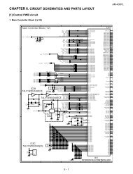
1. MCU PWB . . . . . . . . . . . . . . . . . . . . . . . . . . . . . . . . . . . . .14-1<br />
2. OPERATION PWB . . . . . . . . . . . . . . . . . . . . . . . . . . . . .14-10<br />
3. POWER SUPPLY . . . . . . . . . . . . . . . . . . . . . . . . . . . . . .14-11<br />
4. NOISE FILTER CIRCUIT . . . . . . . . . . . . . . . . . . . . . . . .14-13<br />
5. ACTUAL WIRING DIAGRAM . . . . . . . . . . . . . . . . . . . . .14-15
[1] GENERAL<br />
1. Major functions<br />
Configurations<br />
Item<br />
Descriptions of items<br />
CPM SB/MB 2 Tray SPF R-SPF<br />
Color<br />
Scanner<br />
GDI<br />
printer<br />
CPM: Copy speed (Copies Per Minute)<br />
SB/MB: SB = <strong>Manual</strong> feed single bypass, MB = <strong>Manual</strong> feed multi bypass<br />
2 tray: Second cassette unit.<br />
SPF: Original feed unit<br />
R-SPF: Duplex original feed unit<br />
Color scanner: Color scanner function<br />
GDI printer: GDI printer function with USB.<br />
PCL printer: PCL printer function with USB.<br />
SOPM: Scan Once Print Many function (Many copies are made by one scan.)<br />
Duplex: Auto duplex copy function<br />
Memory: Standard page memory<br />
FAX: FAX function.<br />
Descriptions of table<br />
: Standard provision<br />
: No function or no option available<br />
Opt: Option<br />
∗1: AL-12PKM<br />
∗2: <strong>AR</strong>-PG2<br />
<strong>AR</strong>-<strong>122E</strong>/<strong>152E</strong>/<strong>153E</strong>/<strong>157E</strong> GENERAL 1 - 1<br />
PCL<br />
printer<br />
SOPM Duplex Memory FAX<br />
Model<br />
<strong>AR</strong>-<strong>122E</strong> 12CPM SB Opt ∗1 Opt ∗1 8M<br />
<strong>AR</strong>-<strong>152E</strong> 15CPM SB Opt ∗1 Opt ∗1 8M<br />
<strong>AR</strong>-<strong>153E</strong> 15CPM MB Opt Opt Opt ∗2 Opt ∗2 8M<br />
<strong>AR</strong>-<strong>157E</strong> 15CPM MB Opt ∗2 Opt ∗2 16M<br />
(Options)<br />
<strong>AR</strong>-SP5<br />
<strong>AR</strong>-<strong>122E</strong>/<strong>152E</strong>/<strong>153E</strong><br />
<strong>AR</strong>-D16<br />
AL-12PKM<br />
<strong>AR</strong>-<strong>157E</strong><br />
<strong>AR</strong>-PG2
[2] SPECIFICATIONS<br />
1. Basic Specifications<br />
Item<br />
Type Desktop<br />
Copy system Dry, electrostatic<br />
Segment (class) Digital personal copier<br />
Copier dimensions <strong>AR</strong>-<strong>122E</strong> 20.4"(W)X18.2"(D)X11.6"(H) (518mm(W)X462.5mm(D)X295.6mm(H))<br />
<strong>AR</strong>-<strong>152E</strong> 20.4"(W)X18.2"(D)X11.6"(H) (518mm(W)X462.5mm(D)X295.6mm(H))<br />
<strong>AR</strong>-<strong>153E</strong> 20.4"(W)X19.4"(D)X11.6"(H) (518mm(W)X492.5mm(D)X295.6mm(H))<br />
<strong>AR</strong>-<strong>157E</strong> 20.4"(W)X19.4"(D)X18.3"(H) (518mm(W)X492.5mm(D)X465.4mm(H))<br />
Weight<br />
(Approximately)<br />
2. Operation specifications<br />
Paper feed<br />
section<br />
<strong>AR</strong>-<strong>122E</strong> 35.3lbs.(17Kg) TD and drum cartridges included<br />
<strong>AR</strong>-<strong>152E</strong> 35.3lbs.(17Kg)<br />
<strong>AR</strong>-<strong>153E</strong> 35.3lbs.(17Kg)<br />
<strong>AR</strong>-<strong>157E</strong> 50.7lbs.(24Kg)<br />
Section, item Details<br />
Paper feed<br />
system<br />
AB system Tray paper feed<br />
section<br />
Multi bypass paper<br />
feed section<br />
Single bypass paper<br />
feed section<br />
Inch system Tray paper feed<br />
section<br />
Multi bypass paper<br />
feed section<br />
Single bypass paper<br />
feed section<br />
<strong>AR</strong>-<strong>122E</strong>/<strong>152E</strong> 1 tray (250 sheet) + single bypass<br />
<strong>AR</strong>-<strong>153E</strong> 1 tray (250 sheet) + multi bypass (50 sheet)<br />
<strong>AR</strong>-<strong>157E</strong> 2 tray (500 sheet) + multi bypass (50 sheet)<br />
Paper size A4, B5, A5 (Landscape)<br />
Paper weight 56 - 80g/m2 (15 - 21 lbs.)<br />
Paper feed capacity 250 sheets<br />
Kinds Standard paper, specified paper, recycled paper<br />
Remark User adjustment of paper guide available<br />
Paper size A4, B5, A5, B6, A6 (Landscape)<br />
Paper weight 52 - 128g/m2 (14 - 34.5 lbs.)<br />
Paper feed capacity 50 sheets<br />
Kinds Standard paper, specified paper, recycled paper, OHP,<br />
Label, Envelop (Single copy)<br />
Remark User adjustment of paper guide available<br />
Paper size A4, B5, A5, B6, A6 (Landscape)<br />
Paper weight 52 - 128g/m2 (14 - 34.5 lbs.)<br />
Paper feed capacity 1 sheet<br />
Kinds Standard paper, specified paper, recycled paper, OHP,<br />
Label, Postal card, Envelop, Post card (Including<br />
double postal without fold line)<br />
Remark User adjustment of paper guide available<br />
Paper size 8-1/2" x 14", 8-1/2 x 11", 8-1/2" x 5-1/2" (Landscape)<br />
Paper weight 15 - 21 lbs.<br />
Paper feed capacity 250 sheets<br />
Kinds Standard paper, specified paper, recycled paper<br />
Remark User adjustment of paper guide available<br />
Paper size 8-1/2" x 14", 8-1/2 x 11", 8-1/2" x 5-1/2", 3-1/2" x 5-1/2"<br />
(Landscape)<br />
Paper weight 14 - 34.5 lbs.<br />
Paper feed capacity 50 sheets<br />
Kinds Standard paper, specified paper, recycled paper, OHP,<br />
Label, Envelop (Single copy)<br />
Remark User adjustment of paper guide available<br />
Paper size 8-1/2" x 14", 8-1/2 x 11", 8-1/2" x 5-1/2" (Landscape)<br />
Paper weight 14 - 34.5 lbs.<br />
Paper feed capacity 1 sheet<br />
Kinds Standard paper, specified paper, recycled paper, OHP,<br />
Label, Envelop<br />
Remark User adjustment of paper guide available<br />
Paper exit section Exit way Face down<br />
Capacity of output tray 100 sheets<br />
Originals Original set Center Registration (left edge)<br />
Max. original size A4 (8-1/2" x 14")<br />
Original kinds sheet, book<br />
Original size detection None<br />
<strong>AR</strong>-<strong>122E</strong>/<strong>152E</strong>/<strong>153E</strong>/<strong>157E</strong> SPECIFICATIONS 2 - 1
Optical section Scanning<br />
section<br />
Section, item Details<br />
Writing<br />
section<br />
Scanning system 3 CCDs (R<strong>GB</strong>) sensor scanning by lighting white lamp<br />
CCD sensor Resolution 600 dpi<br />
Lighting lamp Type CCFL<br />
Voltage 1100Vrms (Min)<br />
Power consumption 9.6W (Max)<br />
Output data R, G, B 1 or 8 bits/pixel / A/D 16bit<br />
Writing system Writing to OPC drum by the semiconductor laser<br />
Laser unit Resolution 600 dpi<br />
Image forming Photoconductor type OPC (30ø)<br />
Life 25k<br />
Charger Charging system Saw -tooth charging with a grid, / (-) scorotron<br />
discharge<br />
Transfer system (+) DC scorotron system<br />
Separation system (-) DC scorotron system<br />
Developing Developing system Dry, 2-component magnetic brush development system<br />
Cleaning Cleaning system Counter blade system (Counter to rotation)<br />
Fusing section Fusing system Heat roller system<br />
Upper heat roller type Teflon roller<br />
Lower heat roller type Silicon rubber roller<br />
Heater lamp type Halogen lamp<br />
Voltage 120V/230V<br />
Power consumption 800W<br />
Electrical section Power source Voltage 100V, 110V, 120/127V, 230V, 240V<br />
Frequency Common use for 50 and 60Hz<br />
Power consumption Max. Less than 1000W<br />
Average<br />
(during copying)<br />
*1) May fluctuate due to environmental conditions and the input voltage.<br />
<strong>AR</strong>-<strong>122E</strong> 300 Wh/H *1)<br />
<strong>AR</strong>-<strong>152E</strong> 300 Wh/H *1)<br />
<strong>AR</strong>-<strong>153E</strong> 300 Wh/H *1)<br />
<strong>AR</strong>-<strong>157E</strong> 310 Wh/H *1)<br />
Average (stand-by) 80Wh/H *1)<br />
Pre-heat mode 18Wh/H *1)<br />
Auto power shut-off mode 4.5Wh/H *1)<br />
<strong>AR</strong>-<strong>122E</strong>/<strong>152E</strong>/<strong>153E</strong>/<strong>157E</strong> SPECIFICATIONS 2 - 2
3. Copy performance<br />
4. RSPF<br />
Section, item Details <strong>AR</strong>-<strong>122E</strong> <strong>AR</strong>-<strong>152E</strong> <strong>AR</strong>-<strong>153E</strong> <strong>AR</strong>-<strong>157E</strong><br />
Copy magnification Fixed<br />
magnification<br />
ratios<br />
Zooming<br />
magnification<br />
ratios<br />
<strong>Manual</strong> steps<br />
(manual, photo)<br />
3 Reduction + 2 Enlargement<br />
(AB system : 25, 70, 86, 100, 141, 400%)<br />
(Inch system : 25, 64, 78, 100, 129, 400%)<br />
25 - 400%<br />
(376 steps in 1% increments)<br />
Copy speed First copy time Tray paper feed 9.6 sec. (Pre-heat mode:25 sec. / Auto power-shut-off mode : 40 sec.)<br />
A4 or Letter/100%/Auto Exposure<br />
AB system Copy speed Same size 12 15 15 15<br />
A4<br />
(CPM) Enlargement 12 15 15 15<br />
(Landscape)<br />
Reduction 12 15 15 15<br />
AB system Copy speed Same size 12 15 15 15<br />
B5<br />
(CPM) Enlargement 12 15 15 15<br />
(Landscape)<br />
Reduction 12 15 15 15<br />
Inch system Copy speed Same size 12 12 12 12<br />
8-1/2" x 14" (CPM) Enlargement 12 12 12 12<br />
(Landscape)<br />
Reduction 12 12 12 12<br />
Inch system Copy speed Same size 12 15 15 15<br />
8-1/2" x 11" (CPM) Enlargement 12 15 15 15<br />
(Landscape)<br />
Reduction 12 15 15 15<br />
Max. continuous copy quantity 99<br />
Void Void area leading edge 1 - 4mm<br />
Trailing edge 4mm or less, 6mm or less (Duplex copying/both image)<br />
Side edge void area 0.5mm or more (per side)<br />
4.5mm or less (total of both sides)<br />
Image loss leading edge same size: 3.0mm or less (OC) / 4mm or less (SPF/R-SPF/Duplex)<br />
Enlarge: 2mm or less (OC) / 3mm or less (SPF/R-SPF/Duplex)<br />
Reduction (50%): 6.0mm or less (OC) / 8mm or less (SPF/R-SPF/<br />
Duplex)<br />
Warm-up time 0 sec.<br />
Power save mode reset time 0 sec.<br />
Paper jam recovery time 0 sec.<br />
Original capacity 30 sheets (52 to 90g/m 2 )(14 to 23.9 lbs.)<br />
Original size A4 to A5/10" x 14" to 5-1/2" x 8-1/2"<br />
Original replacement speed 12CPM(A4/8-1/2" x 11"Landscape)(15CPM model)<br />
Job speed(Tray1,Landscape) Single copy S to S 12CPM<br />
S to D 5.6CPM<br />
D to S 5.5CPM<br />
D to D 5.2CPM<br />
Multi copy S to S 15CPM<br />
D to S 15CPM<br />
Original placement Face up<br />
Original weight 52 to 90g/m 2 (14 - 23.9lbs.)<br />
Mixed feeding(Paper size) Performance Degraded<br />
Original which cannot Thermal papers, originals with punch holes for files, be used folded paper, transparent<br />
originals such as OHP films, stapled or clip used originals with cover up liquid used,<br />
Originals with tape sealed, originals with high level frictional coefficient such as photos or<br />
catalogs.<br />
5 steps<br />
<strong>AR</strong>-<strong>122E</strong>/<strong>152E</strong>/<strong>153E</strong>/<strong>157E</strong> SPECIFICATIONS 2 - 3
[3] CONSUMABLE P<strong>AR</strong>TS<br />
1. Supply system table<br />
A. SEC governments<br />
No. Name Content Life Product name Package Remark<br />
1 Toner CA(Black) Toner<br />
× 10 80K <strong>AR</strong>-152MT-J 1 ∗ Life setup is based on A4<br />
(Toner: Net Weight 210g)<br />
6%.<br />
Polyethylene bag × 10<br />
MT=NT ∗10<br />
B. SEC/SECL/LAG<br />
No. Name Content Life Product name Package Remark<br />
1 Toner CA(Black) Toner<br />
× 10 80K <strong>AR</strong>-152MT 1 ∗ Life setup is based on A4<br />
(Toner: Net Weight 210g)<br />
6%.<br />
Polyethylene bag × 10<br />
MT=NT ∗10<br />
2 Developer Developer<br />
(Developer: Net Weight 170g)<br />
× 10 250K <strong>AR</strong>-152MD 1 MD=ND ∗10<br />
3 Drum kit Drum × 1 25K <strong>AR</strong>-152DR 10<br />
Drum fixing plate × 1<br />
Note: Printing of the master/individual cartons is made in 2 languages, English/French.<br />
Packed together with the machine: DR 25K/Developer UN/Process UN<br />
C. Europe subsidiaries/East Europe/SCA/SCNZ<br />
No. Name Content Life Product name Package Remark<br />
1 Toner CA(Black) Toner<br />
(Toner: Net Weight 210g)<br />
× 10 80K <strong>AR</strong>-152LT 1 LT=T ∗10<br />
Polyethylene bag × 10<br />
2 Developer Developer<br />
(Developer: Net Weight 170g)<br />
× 10 250K <strong>AR</strong>-152LD 1 LD=DV ∗10<br />
3 Drum kit Drum × 1 25K <strong>AR</strong>-152DM 10<br />
Drum fixing plate × 1<br />
Note: Printing of the master/individual cartons is made in 4 languages, English/French/German/Spanish.<br />
Packed together with the machine: DR 25K/Developer UN/Process UN<br />
D. SMEF (Middle East, Africa) Israel/Russia/CIS/Taiwan/Philippines<br />
No. Name Content Life Product name Package Remark<br />
1 Toner CA(Black) Toner<br />
× 10 80K <strong>AR</strong>-<strong>152E</strong>T 1 ∗ Life setup is based on A4<br />
(Toner: Net Weight 210g)<br />
6%.<br />
Polyethylene bag × 10<br />
ET=FT ∗10<br />
2 Developer Developer<br />
(Developer: Net Weight 170g)<br />
× 10 250K <strong>AR</strong>-152CD 1 CD=SD ∗10<br />
3 Drum kit Drum × 1 25K <strong>AR</strong>-152DR 10<br />
Drum fixing plate × 1<br />
Note: Printing of the master/individual cartons is made in 4 languages, English/French/German/Spanish.<br />
Packed together with the machine: DR 25K/Developer UN/Process UN<br />
E. Asia (Subsidiary)<br />
No. Name Content Life Product name Package Remark<br />
1 Toner CA(Black) Toner<br />
× 10 80K <strong>AR</strong>-152CT 1 ∗ Life setup is based on A4<br />
(Toner: Net Weight 210g)<br />
6%.<br />
Polyethylene bag × 10<br />
CT=ST ∗10<br />
2 Developer Developer<br />
(Developer: Net Weight 170g)<br />
× 10 250K <strong>AR</strong>-152CD 1 CD=SD ∗10<br />
3 Drum kit Drum × 1 25K <strong>AR</strong>-152DR 10<br />
Drum fixing plate × 1<br />
Note: Printing of the master/individual cartons is made in 4 languages, English/French/German/Spanish.<br />
Packed together with the machine: DR 25K/Developer UN/Process UN<br />
<strong>AR</strong>-<strong>122E</strong>/<strong>152E</strong>/<strong>153E</strong>/<strong>157E</strong> CONSUMABLE P<strong>AR</strong>TS 3 - 1
F. SRH Chinese language version<br />
No. Name Content Life Product name Package Remark<br />
1 Toner CA(Black) Toner (Toner: Net Weight 210g) × 10 80K <strong>AR</strong>-152CT-C 1 ∗ Life setup is based on A4<br />
Polyethylene bag × 10<br />
6%.<br />
CTC=STC ∗10<br />
2 Developer Developer (Developer: Net<br />
Weight 170g)<br />
× 10 250K <strong>AR</strong>-152CD-C 1 CDC=SDC ∗10<br />
3 Drum kit Drum × 1 25K <strong>AR</strong>-152DR-C 10<br />
Drum fixing plate × 1<br />
Note: Printing of the master/individual cartons is made in 2 languages, English/Chinese.<br />
Packed together with the machine: DR 25K/Developer UN/Process UN<br />
2. Environmental<br />
The environmental conditions for assuring the copy quality and the<br />
machine operations are as follows:<br />
(1) Normal operating condition<br />
Temperature: 20°C to 25<br />
Humidity: 65 ± 5%RH<br />
(2) Acceptable operating condition<br />
Humidity (RH)<br />
85%<br />
60%<br />
20%<br />
(3) Optical condition<br />
Humidity (RH)<br />
90%<br />
60%<br />
15%<br />
(4) Supply storage condition<br />
Humidity (RH)<br />
90%<br />
20%<br />
10˚C 30˚C 35˚C<br />
–25˚C 30˚C 40˚C<br />
–5˚C 45˚C<br />
<strong>AR</strong>-<strong>122E</strong>/<strong>152E</strong>/<strong>153E</strong>/<strong>157E</strong> CONSUMABLE P<strong>AR</strong>TS 3 - 2<br />
3. Production control number (lot No.)<br />
identification<br />
<br />
∗: Destination<br />
Division No.<br />
EX Destination<br />
A same pack<br />
B same pack<br />
G<br />
H<br />
Option Destination<br />
A<br />
B<br />
P<br />
Q<br />
<br />
The label on the drum cartridge shows the date of production.<br />
(SOCC production)<br />
<br />
Ver.A 9 1<br />
1<br />
0001<br />
X<br />
Production month<br />
Production day<br />
Destination code<br />
(Dealer, distributor, OEM, etc.)<br />
Production place<br />
(SOCC: Fixed to B.)<br />
End digit of year<br />
Version No.<br />
Production month<br />
Production day<br />
Destination code<br />
(Dealer, distributor, OEM, etc.)<br />
Production place<br />
(SOCC: Fixed to B.)<br />
End digit of year<br />
Version No.<br />
Production month<br />
(1 - 9 = Jan. - Sep. 0 = Oct. X = Nov. Y = Dec.)<br />
Serial number of month<br />
Fixed to 1.<br />
Pack division<br />
(See table below)<br />
End digit of year<br />
Version No.
Division No.<br />
Ex production 1<br />
Option 2<br />
Same pack 3<br />
∗1 The production control label is not attached to the cartridge of a<br />
China product.<br />
<br />
Production control<br />
label attachment position<br />
Production control<br />
label attachment position(*1)<br />
Sub lot<br />
Production day<br />
Production month<br />
End digit of year<br />
Production place<br />
4. TD cartridge replacement<br />
1) Open the front and side cabinets of the copier.<br />
2) Keep holding Toner lover, and<br />
3) Carefully pull out Toner unit from the copier.<br />
<strong>AR</strong>-<strong>122E</strong>/<strong>152E</strong>/<strong>153E</strong>/<strong>157E</strong> CONSUMABLE P<strong>AR</strong>TS 3 - 3<br />
2<br />
3<br />
4) Put Toner unit in a collection bag immediately after removing it<br />
from the copier<br />
Note: Never carry exposed Toner unit. Be sure to put it in the<br />
collection bag.<br />
1
[4] EXTERNAL VIEWS AND INTERNAL STRUCTURES<br />
1. Appearance<br />
1 Original cover 2 Side cover 3 Bypass tray<br />
4 Bypass tray guides 5 Side cover open button 6 Front cover<br />
7 Paper tray 8 Operation panel 9 Original table<br />
10 Document feeder tray 11 SPF exit area *1 / RSPF exit area *2 12 Original guides<br />
13 Feeding roller cover 14 USB interface 15 Parallel interface<br />
16 Paper output tray 17 Paper output tray extension 18 Power switch<br />
19 Handle 20 Power cord<br />
*1 SPF only *2 RSPF only<br />
2. Internal<br />
SPF/RSPF<br />
11<br />
10<br />
9<br />
8<br />
6<br />
7<br />
12<br />
13<br />
5<br />
Single bypass<br />
1<br />
5<br />
Interface<br />
1 14<br />
1 Toner cartridge lock release button 2 Toner cartridge 3 Drum cartridge<br />
4 Drum cartridge handle 5 Fusing unit release lever 6 Charger cleaner<br />
7 Transfer charger<br />
4<br />
2<br />
<strong>AR</strong>-<strong>122E</strong>/<strong>152E</strong>/<strong>153E</strong>/<strong>157E</strong> EXTERNAL VIEWS AND INTERNAL STRUCTURES 4 - 1<br />
6<br />
3<br />
2<br />
4<br />
4<br />
3<br />
7<br />
15<br />
16<br />
17<br />
18<br />
19<br />
20
3. Operation panel<br />
(<strong>AR</strong>-<strong>122E</strong>)<br />
(<strong>AR</strong>-<strong>157E</strong>)<br />
1 Duplex Mode select key and indicator<br />
(RSPF only)<br />
13<br />
Inch system<br />
3 Light and dark keys and exposure indicators<br />
Use to adjust the MANUAL or PHOTO exposure level.<br />
Selected exposure level is shown by a lit indicator.<br />
Use to start and terminate user program setting.<br />
<strong>AR</strong>-<strong>122E</strong>/<strong>152E</strong>/<strong>153E</strong>/<strong>157E</strong> EXTERNAL VIEWS AND INTERNAL STRUCTURES 4 - 2<br />
7<br />
15<br />
10 11 12<br />
16<br />
17<br />
10 11 12<br />
2 Exposure mode selector key and indicators<br />
Use to sequentially select the exposure modes: AUTO, MANUAL or<br />
PHOTO. Selected mode is shown by a lit indicator.<br />
4 Alarm indicators<br />
Developer replacement required indicator<br />
Misfeed indicator<br />
Toner cartridge replacement required indicator *1<br />
Maintenance indicator<br />
5 SPF/RSPF indicator 6 SPF misfeed indicator<br />
7 Copy ratio selector key and copy ratio indicators<br />
Use to sequentially select preset reduction/enlargement copy ratios.<br />
Selected copy ratio is shown by a lit indicator.<br />
8 Copy ratio display (%) key<br />
9 Display<br />
Displays the specified copy quantity, zoom copy ratio, user program<br />
code, and error code.<br />
10 SCANNER key and indicator *2, *3<br />
11 ON LINE key / indicator<br />
12 Power save indicator<br />
Lights up when the machine is used as a printer and scanner. *2 Lights up when the copier is in a power save mode.<br />
13 Paper feed location indicators<br />
14 Tray select key<br />
Light up to show the selected paper feed station.<br />
Use to select a paper feed station (paper tray or bypass tray).<br />
15 Zoom keys / indicator<br />
16 Copy quantity keys<br />
Use to select any reduction or enlargement copy ratio from 25% to • Use to select the desired copy quantity (1 to 99).<br />
400% in 1% increments.<br />
Use to make user program entries.<br />
17 Clear key<br />
18 Print key and ready indicator<br />
Press to clear the display, or press during a copy run to terminate Copying is possible when the indicator is on.<br />
copying.<br />
Use to set a user program.<br />
Press and hold down during standby to display the total number of<br />
copies made to date.<br />
Press to start copying<br />
18
*1. Toner Developer Cartridge Replacement<br />
When toner density is lower than a specified level, the TONER<br />
DEVELOPER C<strong>AR</strong>TRIDGE REPLACEMENT indicator lights up to<br />
warn the user. If the Toner Developer Cartridge is not replaced in<br />
that time, the Ready Lamp changes to blinking and then start to<br />
supply the toner after around 10 copies. (Cartridge replacement<br />
lamp continues to light.) If toner density is not back to specific level<br />
after two minutes, the READY indicator goes out and Toner Developer<br />
indicator starts blinking, and the copier stops.<br />
*2. Indicators on the operation panel<br />
The ON LINE indicator and the start ( ) indicator indicate the<br />
state of the printer or scanner.<br />
Start indicator<br />
On: Indicates the unit is ready for copying or scanning is<br />
being performed.<br />
Blinking: Indicates that an interrupt print job is in progress, or that<br />
the unit is initializing (the cover has been opened and<br />
closed or the power turned off and on).<br />
Off: Indicates copying or scanning is being performed or the<br />
unit is in the auto power shut-off mode.<br />
ON LINE indicator<br />
The ON LINE key is pressed and on line and off line are changed.<br />
Power save indicator<br />
Scanner indicator<br />
SCANNER indicator<br />
ON LINE indicator<br />
Start indicator<br />
Power save indicator<br />
On: Indicates the unit is ready for printing or scanning is<br />
being performed. (On line)<br />
Blinking: Printing or data is being received from a computer.<br />
Off: Copying is being performed. (Off line)<br />
On: Indicates the unit is in a power save mode.<br />
On: The SCANNER ( ) key has been pressed and the unit<br />
is in scanner mode.<br />
Blinking: A scan job is being executed from the computer, or scan<br />
data is stored in the unit's memory.<br />
Off: The unit is in the copy mode.<br />
*3. Using the SCANNER key to begin scanning<br />
This scanning method can only be used if the Button Manager has<br />
been installed using the installer. To scan using this method, you<br />
must first complete the settings in Button Manager in your computer.<br />
For more information on Button Manager, see the online<br />
manual or the help file for Button Manager.<br />
Note:<br />
Scanning is not possible during a copy job.<br />
If the unit is used to begin a scan job during a print job using the<br />
parallel interface connection or the USB interface connection,<br />
the scan job will be stored and scanning will begin when the print<br />
job is completed.<br />
When scanning an original that has been placed in the SPF/<br />
RSPF, only one original can be placed unless you are using<br />
Sharpdesk.<br />
1) Press the SCANNER ( ) key.<br />
The unit enters scan mode.<br />
2) Place the original you wish to scan on the original table/SPF/<br />
RSPF.<br />
For the procedure for placing the original, see "ORIGINAL<br />
PLACEMENT".<br />
3) Press the right copy quantity key to display the number of the<br />
application that you wish to use for scanning.<br />
The application numbers are initially as follows.<br />
The application numbers are initially as follows.<br />
Application<br />
number<br />
Application launched<br />
SC1 Sharpdesk (if installed)<br />
SC2 E-mail (your standard e-mail program in the<br />
Windows OS you are using)<br />
SC3 Fax (if a fax program is installed)<br />
SC4 OCR (if an OCR program is installed)<br />
SC5 Microsoft Word (if installed)<br />
SC6 Any application set in Button Manager<br />
4) Press the start ( ) key.<br />
The selected application launches and scanning begins.<br />
<strong>AR</strong>-<strong>122E</strong>/<strong>152E</strong>/<strong>153E</strong>/<strong>157E</strong> EXTERNAL VIEWS AND INTERNAL STRUCTURES 4 - 3
4. Motors and solenoids<br />
No. Part name Control signal Function / Operation<br />
1 Main motor MM Drives the copier.<br />
2 Scanner motor MRMT Drives the optical mirror base (scanner unit).<br />
3 Toner motor TM Supplies toner.<br />
4 Cooling fan motor VFM Cools the optical section.<br />
5 Resist roller solenoid RRS Resist roller rotation control solenoid<br />
6 Paper feed solenoid CPFS1 Cassette Paper feed solenoid 1<br />
7 Multi paper feed solenoid MPFS Multi manual pages feed solenoid<br />
8 SPF motor SPFM Drives the single pass feeder<br />
9 Duplex motor DMT Devices the duplex paper transport section<br />
10 Original feed solenoid SPUS Original feed solenoid<br />
11 Paper feed solenoid CPFS2 Cassette Paper feed solenoid 2<br />
12 SRRC Original resist roller solenoid<br />
13 SPFS Original paper feed solenoid<br />
<strong>AR</strong>-<strong>122E</strong>/<strong>152E</strong>/<strong>153E</strong>/<strong>157E</strong> EXTERNAL VIEWS AND INTERNAL STRUCTURES 4 - 4<br />
9<br />
13<br />
2<br />
3<br />
8<br />
11<br />
12<br />
6<br />
7<br />
10<br />
4<br />
1<br />
5
5. Sensors and switches<br />
1<br />
8<br />
No. Name Signal Type Function Output<br />
1 Scanner unit home position<br />
sensor<br />
MHPS Transmission sensor Scanner unit home position detection "H" at home position<br />
2 POD sensor POD Transmission sensor Paper exit detection "H" at paper pass<br />
3 PPD2 sensor PPD2 Transmission sensor Paper transport detection 2 "L" at paper pass<br />
4 Cassette detection switch CED1 Micro-switch Cassette installation detection "L" at cassette insertion<br />
5 <strong>Manual</strong> feed detection MFD Transmission sensor <strong>Manual</strong> feed paper detection "L" at paper detection<br />
switch<br />
(single only)<br />
6 PPD1 sensor PPD1 Transmission sensor Paper transport detection 1 "L" at paper pass<br />
7 Door switch DSW Micro-switch Door open/close detection<br />
(safety switch for 24V)<br />
1 or 0V of 24V at door open<br />
8 Drum reset switch DRST Micro-switch New drum detection switch Instantaneously "L" at insertion of new<br />
drum<br />
9 SPF sensor SPID/ Transmission sensor Paper entry detection<br />
"L" at paper pass<br />
SD SW<br />
Cover open/close detection<br />
10 SPPD sensor SPPD Transmission sensor Paper transport detection "L" at paper pass<br />
11 SDOD sensor SDOD Transmission sensor SPF open/close detection Book<br />
sensor<br />
"L" at paper pass<br />
12 2nd cassette DSW Micro-switch 2nd cassette door open detection 1 or 0V of 5V at door open<br />
13 PPD3 sensor PPD3 Transmission sensor Paper transport detection 3 "L" at paper pass<br />
<strong>AR</strong>-<strong>122E</strong>/<strong>152E</strong>/<strong>153E</strong>/<strong>157E</strong> EXTERNAL VIEWS AND INTERNAL STRUCTURES 4 - 5<br />
11<br />
2<br />
7<br />
13<br />
9<br />
6<br />
5<br />
10<br />
4<br />
12<br />
3
6. PWB unit<br />
1<br />
4<br />
5<br />
3<br />
7<br />
No. Name Function<br />
1 Exposure lamp invertor PWB Exposure lamp (CCFL) control<br />
2 Main PWB (MCU) Copier control<br />
3 Operation PWB Operation input/display<br />
4 Power PWB AC power input, DC voltage control, High voltage control<br />
5 CCD sensor PWB For image scanning<br />
6 LSU motor PWB For polygon motor drive<br />
7 TCS PWB For toner sensor control<br />
8 LSU PWB For laser control<br />
9 I/F PWB Scanner/GDI Printer control (parallel I/F, USB I/F)<br />
<strong>AR</strong>-<strong>122E</strong>/<strong>152E</strong>/<strong>153E</strong>/<strong>157E</strong> EXTERNAL VIEWS AND INTERNAL STRUCTURES 4 - 6<br />
9<br />
2<br />
6<br />
8
7. Cross sectional view<br />
1<br />
2<br />
4<br />
3<br />
5<br />
14<br />
<strong>AR</strong>-<strong>122E</strong>/<strong>152E</strong>/<strong>153E</strong>/<strong>157E</strong> EXTERNAL VIEWS AND INTERNAL STRUCTURES 4 - 7<br />
18<br />
13<br />
15 16<br />
No. Part name Function and operation<br />
1 Scanner unit Illuminates the original with the copy lamp and passes the reflected light to the lens unit(CCD).<br />
2 Exposure lamp Exposure lamp (CCFL) Illuminates original<br />
3 LSU (Laser unit) Converts the original image signal into laser beams and writes onto the drum.<br />
4 Paper exit roller Roller for paper exit<br />
5 Main charger Provides negative charges evenly to the drum surface.<br />
6 Heat roller Fuses toner on the paper. (Teflon roller)<br />
7 Pressure roller Fuses toner on the paper. (Silicon rubber roller)<br />
8 Drum Forms images.<br />
9 Transfer unit Transfers images onto the drum.<br />
10 Pickup roller Picks up the manual feed paper. (In multi feed only)<br />
11 <strong>Manual</strong> paper feed tray Tray for manual feed paper<br />
12 <strong>Manual</strong> paper feed roller Transport the paper from the manual paper feed port.<br />
13 PS roller unit Takes synchronization between the lead edge and the rear edge of the paper.<br />
14 Paper feed roller Picks up a sheet of paper from the cassette.<br />
15 Pickup roller Picks up documents.<br />
16 Separation roller Separates documents to feed properly.<br />
17 PS roller Feeds documents to the scanning section.<br />
18 Paper exit roller Discharges documents.<br />
12<br />
17<br />
6<br />
7<br />
8<br />
9<br />
10<br />
11
[5] UNPACKING AND INSTALLATION<br />
1. Copier installation<br />
Improper installation may damage the copier. Please note the following<br />
during initial installation and whenever the copier is moved.<br />
Caution: If the copier is moved from a cool place to a warm place, condensation<br />
may form inside the copier. Operation in this condition<br />
will cause poor copy quality and malfunctions.<br />
Leave the copier at room temperature for at least 2 hours<br />
before use.<br />
Do not install your copier in areas that are:<br />
• damp, humid, or very dusty<br />
exposed to direct sunlight<br />
poorly ventilated<br />
subject to extreme temperature or humidity changes, e.g., near an<br />
air conditioner or heater.<br />
The copier should be installed near an accessible power outlet for easy<br />
connection.<br />
Be sure to connect the power cord only to a power outlet that meets<br />
the specified voltage and current requirements.<br />
Also make certain the outlet is properly grounded.<br />
Be sure to allow the required space around the machine for servicing<br />
and proper ventilation.<br />
4"<br />
(10cm)<br />
8" (20cm)<br />
4"<br />
(10cm)<br />
8"(20cm)<br />
2. Cautions on handling<br />
<strong>AR</strong>-<strong>122E</strong>/<strong>152E</strong>/<strong>153E</strong>/<strong>157E</strong> UNPACKING AND INSTALLATION 5 - 1<br />
Be careful in handling the copier as follows to maintain the performance<br />
of this copier.<br />
Do not drop the copier, subject it to shock or strike it against any<br />
object.<br />
Do not expose the drum cartridge to direct sunlight.<br />
Doing so will damage the surface (green portion) of the drum cartridge,<br />
causing poor print quality.<br />
Store spare supplies such as drum cartridges and TD cartridges in a<br />
dark place without removing from the package before use.<br />
If they are exposed to direct sunlight, poor print quality may result.<br />
Do not touch the surface (green portion) of the drum cartridge.<br />
Doing so will damage the surface of the cartridge, causing poor print<br />
quality.<br />
3. Checking packed components and<br />
accessories<br />
Open the carton and check if the following components and accessories<br />
are included.<br />
Operation manual<br />
Power cord<br />
Drum cartridge<br />
(installed in unit)
4. Unpacking<br />
Be sure to hold the handles on both sides of the copier to unpack the<br />
copier and carry it to the installation location.<br />
5. Removing protective packing materials<br />
1) Remove pieces of tape and protective cover. Then open the original<br />
cover and remove protective materials (a) and (b).<br />
<strong>AR</strong>-<strong>122E</strong>/<strong>152E</strong>/<strong>153E</strong><br />
<strong>AR</strong>-<strong>157E</strong><br />
2) Release the scan head locking switch.<br />
Grasp here and turn in<br />
the direction of the arrow.<br />
Lock Unlock<br />
<strong>AR</strong>-<strong>122E</strong>/<strong>152E</strong>/<strong>153E</strong><br />
<strong>AR</strong>-<strong>157E</strong><br />
3) Ensure that the bypass tray is open and then open the side cover<br />
by pressing the open button on the side cover.<br />
<strong>AR</strong>-<strong>122E</strong>/<strong>152E</strong>/<strong>153E</strong>/<strong>157E</strong> UNPACKING AND INSTALLATION 5 - 2<br />
4) Remove the CAUTION tape from the front cover and remove the<br />
two protective pins from the fusing unit by pulling the strings<br />
upward one at a time.<br />
CAUTION tape<br />
6. Developer unit installation<br />
1) 2) 3) Open the side and front cabinets of the copier.<br />
4) Remove the locking tape of the developer unit.<br />
5) Remove the screw which is fixing the copier and Developer unit.<br />
6) Remove Developer unit slowly from the copier.<br />
7) Remove the screw (1 pc).<br />
8) Remove Upper developer unit.<br />
5<br />
3<br />
1<br />
4<br />
Protective pins<br />
2
9) Shake the aluminum bag to stir developer<br />
10) Supply developer from the aluminum bag to the top of the MX roller<br />
evenly.<br />
Note: Be careful not to splash developer outside Developer unit.<br />
11) Attach Upper developer unit and fix it with a screw.<br />
12) Rotate the MG roller gear to distribute developer evenly.<br />
Note: Never rotate the gear in the reverse direction.<br />
Note: When carrying Developer unit, do not tilt it extremely as<br />
shown with the arrow in the figure below.<br />
(Prevention of splash of developer)<br />
13) Insert Developer unit carefully into the copier.<br />
Note: Quick insertion may result in splash of developer. Be sure to<br />
insert carefully.<br />
14) Confirm that Developer unit is completely inserted to the bottom of<br />
the machine, fix Developer unit and the machine with a screw.<br />
15) Completion of Developer unit installation<br />
7. Toner cartridge installation<br />
<strong>AR</strong>-<strong>122E</strong>/<strong>152E</strong>/<strong>153E</strong>/<strong>157E</strong> UNPACKING AND INSTALLATION 5 - 3<br />
1) To prevent against uneven distribution of toner, hold Toner unit<br />
with both hands and shake it several times horizontally.<br />
2) Hold the section of Toner unit shown in the figure below, remove<br />
the packing tape, and remove the cushion.<br />
3) Pull out the cushion in the arrow direction.<br />
4) Insert Toner unit carefully into the copier.<br />
5) Insert until the hook is engaged with the copier as shown in the figure<br />
below.<br />
6) Pull out the shutter in the arrow direction.<br />
Note: Do not hold and carry the shutter. Otherwise the shutter may<br />
drop and Toner unit may drop.<br />
7) Completion of Toner unit installation<br />
Close the front and side cabinets.
8. Loading copy paper<br />
Note: This copier is equipped with two paper trays. Load copy paper<br />
into the two paper trays.<br />
1) Raise the handle of the paper tray and pull the paper tray out until<br />
it stops.<br />
2) Remove the pressure plate lock. Rotate the pressure plate lock in<br />
the direction of the arrow to remove it while pressing down the<br />
pressure plate of the paper tray.<br />
3) Store the pressure plate lock that was removed in step 2 and the<br />
screw that was removed when unpacking the machine in the front<br />
of the paper tray. To store the pressure plate lock, rotate the lock<br />
to fix it on the relevant location.<br />
4) Adjust the paper guides on the paper tray to the copy paper width<br />
and length.<br />
Squeeze the lever of paper guide (A) and slide the guide to match<br />
with the width of the paper.<br />
Move paper guide (B) to the appropriate slot as marked on the<br />
tray.<br />
Paper<br />
guide (B)<br />
Paper<br />
guide (A)<br />
5) Fan the copy paper and insert it into the tray. Make sure the edges<br />
go under the corner hooks.<br />
Note: Do not load paper above the maximum height line ( ).<br />
Exceeding the line will cause a paper misfeed.<br />
6) Gently push the paper tray back into the copier.<br />
Note: After loading copy paper, to cancel the blinking "H" without<br />
restarting copying, press the clear ( ) key. The "P" in the<br />
display will go out and the ready ( ) indicator will light up.<br />
9. Power to copier<br />
<strong>AR</strong>-<strong>122E</strong>/<strong>152E</strong>/<strong>153E</strong>/<strong>157E</strong> UNPACKING AND INSTALLATION 5 - 4<br />
1) Ensure that the power switch of the copier is in the OFF position.<br />
Insert the attached power cord into the power cord socket at the<br />
rear of the copier.<br />
2) Plug the other end of the power cord into the nearest outlet.<br />
10. Moving<br />
Moving instructions<br />
When moving the unit, follow the procedure below.<br />
Note: When moving this unit, be sure to remove the TD cartridge in<br />
advance.<br />
1) Turn the power switch off and remove the power cord from the outlet.<br />
2) Open the side cover and front cover, in that order. Remove the TD<br />
cartridge and close the front cover and side cover, in that order.<br />
To open and close the side cover and front cover, and to remove<br />
the TD cartridge, see "TD C<strong>AR</strong>TRIDGE REPLACEMENT".<br />
3) Raise the handle of the paper tray and pull the paper tray out until it<br />
stops.<br />
4) Push the center of the pressure plate down until it locks in place<br />
and lock the plate using the pressure plate lock which has been<br />
stored in the front of the paper tray.<br />
5) Push the paper tray back into the unit.<br />
6) Lock the scan head locking switch.<br />
Note: When shipping the unit, the scan head locking switch must be<br />
locked to prevent shipping damage.<br />
7) Close the multi-bypass tray and the paper output tray extension,<br />
and attach the packing materials and tape which were removed<br />
during installation of the unit. See "PREP<strong>AR</strong>ING THE UNIT FOR<br />
INSTALLATION".<br />
8) Pack the unit into the carton. See "CHECKING PACKED COMPO-<br />
NENTS AND ACCESSORIES".
[6] COPY PROCESS<br />
1. Functional diagram<br />
(Basic operation cycle)<br />
To face<br />
down tray<br />
An OPC drum is used for the photoconductor.<br />
(Structure of the OPC drum layers)<br />
Main charger<br />
Laser beam<br />
MG roller<br />
Main high voltage unit<br />
Cleaning blade<br />
Waste toner box<br />
Saw tooth Charge<br />
Cleaning<br />
Paper release Fusing Separation<br />
Heat roller<br />
Heater lamp<br />
Semiconductor laser<br />
Electrode<br />
OPC layer<br />
(20 microns thick)<br />
Pigment layer (0.2<br />
to 0.3 microns thick)<br />
Aluminum drum<br />
Cleaning blade<br />
Exposure<br />
Drum<br />
Transfer<br />
Drum<br />
Resist roller<br />
Focus correction lens<br />
Transfer charger<br />
Transfer high<br />
voltage unit<br />
<strong>AR</strong>-<strong>122E</strong>/<strong>152E</strong>/<strong>153E</strong>/<strong>157E</strong> COPY PROCESS 6 - 1<br />
Transfer unit<br />
Cassette<br />
paper feed<br />
Developing<br />
Synchronization<br />
with drum<br />
Toner<br />
Developer<br />
PS roller<br />
<strong>Manual</strong> feed<br />
Print process<br />
Paper transport route
2. Outline of print process<br />
This printer is a non-impact printer that uses a semiconductor laser<br />
and electrostatic print process. This printer uses an OPC (Organic<br />
Photo Conductor) for its photoconductive material.<br />
First, voltage from the main corona unit charges the drum surface and<br />
a latent image is formed on the drum surface using a laser beam. This<br />
latent image forms a visible image on the drum surface when toner is<br />
applied. The toner image is then transferred onto the print paper by the<br />
transfer corona and fused on the print paper in the fusing section with<br />
a combination of heat and pressure.<br />
Step-1: Charge<br />
Step-2: Exposure<br />
* Latent image is formed on the drum.<br />
Step-3: Developing<br />
Latent image formed on the drum is then changed into visible<br />
image with toner.<br />
Step-4: Transfer<br />
The visible image (toner image) on the drum is transferred<br />
onto the print paper.<br />
Step-5: Cleaning<br />
Residual toner on the drum surface is removed and collected<br />
by the cleaning blade.<br />
Step-6: Optical discharge<br />
Residual charge on the drum surface is removed, by<br />
semiconductor laser beam.<br />
3. Actual print process<br />
Step-1: DC charge<br />
A uniform negative charge is applied over the OPC drum surface by<br />
the main charging unit. Stable potential is maintained by means of the<br />
Scorotron charger.<br />
Positive charges are generated in the aluminum layer.<br />
About<br />
DC5.5KV<br />
( 580V/ 390V)<br />
<strong>AR</strong>-<strong>122E</strong>/<strong>152E</strong>/<strong>153E</strong>/<strong>157E</strong> COPY PROCESS 6 - 2<br />
Step-2: Exposure (laser beam, lens)<br />
A Laser beam is generated from the semiconductor laser and<br />
controlled by the print pattern signal. The laser writes onto the OPC<br />
drum surface through the polygon mirrors and lens. The resistance of<br />
the OPC layer decreases for an area exposed by the laser beam<br />
(corresponding to the print pattern signal). The beam neutralizes the<br />
negative charge. An electrostatic latent image is formed on the drum<br />
surface.<br />
Exposure<br />
(semiconductor laser)<br />
Drum surface charge<br />
after the exposure<br />
Semiconductor laser<br />
Non-image area Image area<br />
OPC layer<br />
Pigment<br />
layer<br />
Aluminum<br />
drum<br />
OPC layer<br />
Pigment<br />
layer<br />
Aluminum<br />
layer
Step-3: Developing (DC bias)<br />
A bias potential is applied to the MG roller in the two component<br />
magnetic brush developing method, and the toner is charged negative<br />
through friction with the carrier.<br />
Non-image area of the drum surface charged with negative potential<br />
repel the toner, whereas the laser exposed portions where no negative<br />
charges exist, attract the toner. As a result, a visible image appears on<br />
the drum surface.<br />
:Carrier (Magnetized particle)<br />
:Toner (Charge negative by friction)<br />
(N) (S) Permanent magnet<br />
(provided in three locations)<br />
DC<br />
400V 8V<br />
N<br />
N<br />
Toner is attracted over the shadowed area because of the developing<br />
bias.<br />
S<br />
MG roller<br />
<strong>AR</strong>-<strong>122E</strong>/<strong>152E</strong>/<strong>153E</strong>/<strong>157E</strong> COPY PROCESS 6 - 3<br />
Step-4: Transfer<br />
The visible image on the drum surface is transferred onto the print<br />
paper by applying a positive charge from the transfer corona to the<br />
backside of the print paper.<br />
About DC 5.2kV<br />
Step-5: Separation<br />
Since the print paper is charged positively by the transfer corona, it is<br />
discharged by the separation corona. The separation corona is<br />
connected to ground.<br />
Step-6: Cleaning<br />
Toner remaining on the drum is removed and collected by the cleaning<br />
blade. It is transported to the waste toner collecting section in the<br />
cleaning unit by the waste toner transport roller.
Step-7: Optical discharge (Semiconductor laser)<br />
Before the drum rotation is stopped, the semiconductor laser is<br />
radiated onto the drum to reduce the electrical resistance in the OPC<br />
layer and eliminate residual charge, providing a uniform state to the<br />
drum surface for the next page to be printed.<br />
When the electrical resistance is reduced, positive charges on the<br />
aluminum layer are moved and neutralized with negative charges on<br />
the OPC layer.<br />
Charge by the Scorotron charger<br />
Function<br />
The Scorotron charger functions to maintain uniform surface potential<br />
on the drum at all times, It control the surface potential regardless of<br />
the charge characteristics of the photoconductor.<br />
Basic function<br />
A screen grid is placed between the saw tooth and the<br />
photoconductor. A stable voltage is added to the screen grid to<br />
maintain the corona current on the photoconductor.<br />
As the photoconductor is charged by the saw tooth from the main<br />
corona unit, the surface potential increases. This increases the current<br />
flowing through the screen grid. When the photoconductor potential<br />
nears the grid potential, the current turns to flow to the grid so that the<br />
photoconductor potential can be maintained at a stable level.<br />
Process controlling<br />
Function<br />
The print pattern signal is converted into an invisible image by the<br />
semiconductor laser using negative to positive (reversible) developing<br />
method. Therefore, if the developing bias is added before the drum is<br />
charged, toner is attracted onto the drum. If the developing bias is not<br />
added when the drum is charged, the carrier is attracted to the drum<br />
because of the strong electrostatic force of the drum.<br />
To avoid this, the process is controlled by adjusting the drum potential<br />
and the grid potential of the Scorotron charger.<br />
Basic function<br />
Voltage added to the screen grid can be selected, high and low. To<br />
make it easily understood, the figure below shows voltage transition at<br />
the developer unit.<br />
0<br />
Semiconductor laser<br />
ST<strong>AR</strong>T STOP<br />
Print potential<br />
1) Low<br />
2)<br />
3)<br />
4) High<br />
Toner attract<br />
potential<br />
Time<br />
Developing bias<br />
Drum potential<br />
Start<br />
<strong>AR</strong>-<strong>122E</strong>/<strong>152E</strong>/<strong>153E</strong>/<strong>157E</strong> COPY PROCESS 6 - 4<br />
1) Because the grid potential is at a low level, the drum potential is at<br />
about -400V. (Carrier may not be attracted though the carrier is<br />
pulled towards the drum by the electrostatic force of -400V.<br />
2) Developing bias (-400V) is applied when the photoconductor<br />
potential is switched from LOW to HIGH.<br />
3) Once developing bias (-400V) is applied and the photo conductor<br />
potential rises to HIGH, toner will not be attracted to the drum.<br />
Stop<br />
The reverse sequence takes place.<br />
Retaining developing bias at an abnormal occurrence<br />
Function<br />
The developing bias will be lost if the power supply was removed<br />
during print process. In this event, the drum potential slightly abates<br />
and the carrier makes deposits on the drum because of strong static<br />
power. To prevent this, the machine incorporates a function to retain<br />
the developing bias for a certain period and decrease the voltage<br />
gradually against possible power loss.<br />
Basic function<br />
Normally, the developing bias voltage is retained for a certain time<br />
before the drum comes to a complete stop if the machine should stop<br />
before completing the normal print cycle. The developing bias can be<br />
added before resuming the operation after an abnormal interruption.<br />
Therefore, carrier will not make a deposit on the drum surface.
[7] OPERATIONAL DESCRIPTIONS<br />
1. Outline of operation<br />
The outline of operation is described referring to the basic configuration.<br />
(Basic configuration)<br />
Operation<br />
section<br />
Printer section<br />
(Outline of copy operation)<br />
CCD<br />
Scanner section<br />
MCU (Main control/image process section)<br />
Laser beam<br />
Process section<br />
LSU (Laser unit)<br />
Laser diode, Polygon mirror lens<br />
Cassette paper<br />
feed section<br />
Paper exit<br />
Setting conditions<br />
1) Set copy conditions such as the copy quantity and the copy density<br />
with the operation section, and press the COPY button. The<br />
information on copy conditions is sent to the MCU.<br />
Image scanning<br />
2) When the COPY button is pressed, the scanner section starts<br />
scanning of images.<br />
The light from the copy lamp is reflected by the document and<br />
passed through the lens to the CCD.<br />
Photo signal/Electric signal conversion<br />
3) The image is converted into electrical signals by the CCD circuit<br />
and passed to the MCU.<br />
Image process<br />
4) The document image signal sent from the CCD circuit is processed<br />
under the revised conditions and sent to the LSU (laser unit) as<br />
print data.<br />
Electric signal/Photo signal (laser beam) conversion<br />
5) The LSU emits laser beams according to the print data.<br />
(Electrical signals are converted into photo signals.)<br />
6) The laser beams are radiated through the polygon mirror and<br />
various lenses to the OPC drum.<br />
<strong>Manual</strong> paper<br />
feed section<br />
Fusing section<br />
Paper transport section<br />
<strong>AR</strong>-<strong>122E</strong>/<strong>152E</strong>/<strong>153E</strong>/<strong>157E</strong> OPERATIONAL DESCRIPTIONS 7 - 1<br />
Printer/<br />
Scanner I/F USB or Parallel<br />
Note: The scanner function is effective<br />
only by USB connection.<br />
Printing<br />
7) Electrostatic latent images are formed on the OPC drum according<br />
to the laser beams, and the latent images are developed to be<br />
visible images(toner images).<br />
8) Meanwhile the paper is fed to the image transfer section in<br />
synchronization with the image lead edge.<br />
9) After the transfer of toner images onto the paper, the toner images<br />
are fused to the paper by the fusing section. The copied paper is<br />
discharged onto the exit tray.<br />
(Outline of printer operation)<br />
The print data sent from the PC are passed through the I/F and the<br />
MCU to the LSU. The procedures after that are the same as above 5)<br />
and later.<br />
(Outline of scanner operation)<br />
The scan data are passed through the MCU and the I/F to the PC<br />
according to the conditions requested by the PC or set by the operations<br />
with the operation panel.<br />
PC
2. Scanner section<br />
A. Scanner unit<br />
The scanner unit in the digital copier scans images.<br />
It is composed of the optical unit and the drive unit. The optical unit<br />
performs scanning in the main scan direction with the light receiving<br />
elements (color CCD). The drive unit performs scanning in the sub<br />
scanning direction by moving the optical unit.<br />
B. Optical system<br />
Two white lamps are used as the light source.<br />
Light radiated from the light source is applied to the document on the<br />
document table. The reflected light from the document is reflected 5<br />
times by No. 1 - No. 3 mirrors and passed through the reduction lens to<br />
form images on the light-receiving surface of 3-line CCD.<br />
The light-receiving surface of the color CCD is provided with 3 line<br />
scanning sections for R<strong>GB</strong>. Separate images scanned in each color<br />
section are overlapped to complete color scanning. (When PC scanning)<br />
The resolution is 600dpi.<br />
When copying, only the green component is used to print with the<br />
printer.<br />
The color component for printing can be switched to red or blue by the<br />
service simulation.<br />
Intensity of UV<br />
6.00E-01<br />
5.00E-01<br />
4.00E-01<br />
3.00E-01<br />
2.00E-01<br />
1.00E-01<br />
0.00E+00<br />
C. Drive system<br />
Lamp : MBVM26W25W260NLH/G<br />
Lamp current : 5mA<br />
Temp. : 25 degree<br />
MBVM26W25W260NLH/G<br />
0 200 400 600 800<br />
Wave length (nm)<br />
(Spectrum characteristics of the lamp)<br />
The drive system is composed of the scanner motor, the pulley gear,<br />
the idle pulley, the idle gear, the belt 473, the belt 190, and the shaft.<br />
The motor rotation is converted into reciprocated movements of the<br />
belt 473 through the idle gear, the pulley gear, the belt 190, and the<br />
idle pulley to drive the optical unit.<br />
7<br />
<strong>AR</strong>-<strong>122E</strong>/<strong>152E</strong>/<strong>153E</strong>/<strong>157E</strong> OPERATIONAL DESCRIPTIONS 7 - 2<br />
1<br />
7<br />
(Spectrum characteristics of the color CCD)<br />
3<br />
9<br />
5<br />
8<br />
10 8<br />
(Optical unit)<br />
1 Table glass 2 Optical unit 3 Lens<br />
4 Mirror 1 5 Mirror 2 6 Mirror 3<br />
7 CCD PWB 8 Lamp 9 Reflector<br />
3 4 6 2 8 5<br />
1 Scanner motor 2 Pulley gear 3 Idle pulley<br />
4 Belt 473 5 Belt 190 6 Optical unit<br />
7 Shaft 8 Idle gear 9<br />
1<br />
4<br />
9<br />
6<br />
2<br />
3
3. Laser unit<br />
The image data sent from the MCU (image process circuit) is sent to<br />
the LSU (laser unit), where it is converted into laser beams.<br />
A. Basic structure<br />
The LSU unit is the writing section of the digital optical system.<br />
The semiconductor laser is used as the light source, and images are<br />
formed on the OPC drum by the polygon mirror and fθ lens, etc.<br />
The laser beams are passed through the collimator lens, the cylindrical<br />
lens, the polygon mirror, the fθ lens, and the mirror to form images on<br />
the OPC drum in the main scanning direction. The laser emitting PWB<br />
is provided with the APC (auto power control) in order to eliminate fluctuations<br />
in the laser power. The BD PWB works for measurement of<br />
the laser writing start point.<br />
1 2 3<br />
No Component Function<br />
1 Semiconductor laser Generates laser beams.<br />
2 Collimator lens Converges laser beams in parallel.<br />
3 Polygon mirror,<br />
polygon motor<br />
Reflects laser beams at a constant rpm.<br />
4 BD (Mirror, lens, PWB) Detects start timing of laser scanning.<br />
5 fθ lens Converges laser beams at a spot on the<br />
drum.<br />
Makes the laser scanning speeds at both<br />
ends of the drum same as each other.<br />
(Refer to the figure below.)<br />
Makes the laser scanning speeds at both ends of the drum same as<br />
each other.<br />
a ≠ b ≠ c<br />
a b c<br />
4 5<br />
fθ LENS<br />
d = e = f<br />
d e f<br />
B. Laser beam path<br />
C. Composition<br />
<strong>AR</strong>-<strong>122E</strong>/<strong>152E</strong>/<strong>153E</strong>/<strong>157E</strong> OPERATIONAL DESCRIPTIONS 7 - 3<br />
Effective scanning width: 216mm (max.)<br />
Resolution: 600dpi<br />
Beam diameter: 75um in the main scanning direction, 80um in the sub<br />
scanning direction<br />
Image surface power: 0.17 ±0.01mW (Laser wavelength 770 - 795nm)<br />
Polygon motor section: Brushless motor 20.787rpm<br />
No. of mirror surfaces: 6 surfaces<br />
4. Fuser section
A. General description<br />
General block diagram (cross section)<br />
Top view<br />
Thermistor<br />
Heat roller<br />
(1) Heat roller<br />
Thermal fuse<br />
Heat roller<br />
Thermistor<br />
Separator pawl<br />
Paper guide<br />
PPD2<br />
Pressure roller<br />
Thermal fuse<br />
Heater lamp<br />
A Teflon roller is used for the heat roller and a silicone rubber roller is<br />
used for the lower heat roller for better toner fusing performance and<br />
paper separation.<br />
(2) Separator pawl<br />
Three separator pawls are used on the upper heat roller. The separator<br />
pawls are Teflon coated to reduce friction with the roller and prevent<br />
a smear on the paper caused by the separator pawl.<br />
(3) Thermal control<br />
1) The heater lamp, thermistor, main PWB, DC power supply PWB,<br />
and triac within the power supply unit are used to control the<br />
temperature in the fuser unit.<br />
To prevent against abnormally high temperature in the fuser unit, a<br />
thermal breaker and thermal fuse are used for safety purposes.<br />
Safety device<br />
(thermal breaker, thermal<br />
fuse)<br />
Triac (in the<br />
power supply unit)<br />
Separator pawl<br />
Heated by the heater<br />
lamp. (950W)<br />
The surface temperature<br />
of the upper heat roller is<br />
sensed by the thermistor.<br />
Level of the thermistor is<br />
controlled by the main PWB.<br />
With the signal from the<br />
main PWB, the triac is<br />
controlled on and off.<br />
(power supply PWB)<br />
<strong>AR</strong>-<strong>122E</strong>/<strong>152E</strong>/<strong>153E</strong>/<strong>157E</strong> OPERATIONAL DESCRIPTIONS 7 - 4<br />
2) The surface temperature of the upper heat roller is set to 165 -<br />
190°C. The surface temperature during the power save mode is<br />
set to 100°C.<br />
3) The self-check function comes active when one of the following<br />
malfunctions occurs, and an "H" is displayed on the multicopy<br />
window.<br />
a. When the heat roller surface temperature rises above 240°C.<br />
b. When the heat roller surface temperature drops below 100°C during<br />
the copy cycle.<br />
c. Open thermistor<br />
d. Open thermal fuse<br />
e. When the heat roller temperature does not reach 190°C within 27<br />
second after supplying the power.<br />
(4) Fusing resistor<br />
Fusing resistor<br />
This model is provided with a fusing resistor in the fusing section to<br />
improve transfer efficiency.<br />
Since the upper heat roller is conductive, when using copy paper that<br />
contains moisture and the distance between the transfer unit and the<br />
fusing unit is short, the transfer current may find a path to ground via<br />
the copy paper, the upper heat roller and the discharging brush.<br />
5. Paper feed section and paper transport<br />
section<br />
A. Paper transport path and general operations<br />
4 3<br />
14<br />
5<br />
1 Scanner unit 8 Drum<br />
2 Copy lamp 9 Transfer unit<br />
3 LSU (Laser unit) 10 Pickup roller<br />
4 Paper exit roller 11 <strong>Manual</strong> paper feed tray<br />
5 Main charger 12 <strong>Manual</strong> paper feed roller<br />
6 Heat roller 13 PS roller unit<br />
7 Pressure roller 14 Paper feed roller<br />
Paper feed is made in two ways; the tray paper feed and the manual<br />
paper feed. The tray is of universal-type, and has the capacity of 250<br />
sheets.<br />
The front loading system allows you to install or remove the tray from<br />
the front cabinet.<br />
The general descriptions on the tray paper feed and the manual paper<br />
feed operation are given below.<br />
13<br />
12<br />
2<br />
1<br />
6<br />
7<br />
8<br />
9<br />
10<br />
11
(1) Cassette paper feed operation<br />
1) The figure below shows the positions of the pick-up roller, the<br />
paper feed clutch sleeve, and the paper feed latch in the initial<br />
state without pressing the COPY button after lighting the ready<br />
lamp.<br />
The paper feed latch is in contact with the projection of the clutch<br />
sleeve.<br />
2) When the COPY button is pressed, the main drive motor starts<br />
rotating to drive each drive gear.<br />
The pick-up drive gear also is driven at that time. Since, however,<br />
the paper feed latch is in contact with the projection of the clutch<br />
sleeve, rotation of the drive gear is not transmitted to the pick-up<br />
roller, which does not rotate therefore.<br />
PFS<br />
OFF<br />
3) After about 0.1 sec from when the main motor start rotating, the<br />
tray paper feed solenoid (PFS) turns on for a moment.<br />
This disengages the paper feed latch from the projection of the<br />
clutch sleeve, transmitting rotation of the pick-up drive gear to the<br />
paper feed roller shaft, rotating the pick-up roller to feed the paper.<br />
PFS<br />
OFF<br />
RRS<br />
OFF<br />
RRS<br />
OFF<br />
4) After more than half rotation of the pick-up roller, the paper feed<br />
latch is brought in contact with a notch on the clutch sleeve,<br />
stopping rotation of the pick-up roller.<br />
<strong>AR</strong>-<strong>122E</strong>/<strong>152E</strong>/<strong>153E</strong>/<strong>157E</strong> OPERATIONAL DESCRIPTIONS 7 - 5<br />
5) At this time, the paper is fed passed the paper entry detection<br />
switch (PPD1), and detected by it. After about 0.15 sec from<br />
detection of paper by PPD1, the tray paper feed solenoid (PFS)<br />
turns on so that the clutch sleeve projection comes into contact<br />
with the paper feed latch to stop the pick-up roller. Then the pickup<br />
roller rotates for about 0.15 sec so that the lead edge of the<br />
paper is evenly pressed on the resist roller, preventing against<br />
skew feeding.<br />
PFS<br />
ON<br />
6) To release the resist roller, the tray paper feed solenoid and the<br />
resist solenoid are turned on by the paper start signal to disengage<br />
the resist start latch from the clutch sleeve, transmitting rotation of<br />
the resist drive gear to the resist roller shaft. Thus the paper is<br />
transported by the resist roller.<br />
7) After the resist roller starts rotating, the paper is passed through<br />
the pre-transfer guide to the transfer section. Images are<br />
transferred on the paper, which is separated from the OPC drum<br />
by the drum curve and the separation section.<br />
PFS<br />
OFF<br />
RRS<br />
OFF<br />
RRS<br />
ON<br />
8) The paper separated from the drum is passed through the fusing<br />
paper guide, the heat roller (fusing section), POD (paper out<br />
detector) to the copy tray.
(2) <strong>Manual</strong> multi paper feed operation<br />
1) Before paper feed operation, the manual paper feed solenoid<br />
(MPFS) is turned OFF as shown in the figure below.<br />
OFF<br />
MPFS<br />
2) When the PRINT button is pressed, the manual paper feed<br />
solenoid (MPFS) turns on to disengage the manual paper feed<br />
latch.<br />
A from the manual paper feed clutch sleeve A, rotating the manual<br />
paper feed roller and the manual take-up roller. At the same time,<br />
the manual paper feed stopper opens and the manual take-up<br />
roller is pressed to the surface of the paper to start paper feeding.<br />
ON<br />
MPFS<br />
C<br />
C<br />
A<br />
A<br />
<strong>AR</strong>-<strong>122E</strong>/<strong>152E</strong>/<strong>153E</strong>/<strong>157E</strong> OPERATIONAL DESCRIPTIONS 7 - 6<br />
3) When pawl C of the manual paper feed clutch sleeve is engaged<br />
with the manual feed latch, the manual feed stopper falls and the<br />
manual take-up roller rises. At that time, the manual paper feed<br />
roller is rotating.<br />
ON<br />
MPFS<br />
4) The lead edge of the transported paper is pressed on the resist<br />
roller by the transport roller. Then the paper is stopped temporarily<br />
to allow synchronization with the lead edge of the image on the<br />
OPC drum.<br />
From this point, the operation is the same as the paper feed<br />
operation from the tray. (Refer to A-5 - 8.)<br />
5) The solenoid turns off to close the gate and return to the initial<br />
state.<br />
OFF<br />
MPFS<br />
C<br />
C<br />
A<br />
A
(3) Conditions of occurrence of paper misfeed<br />
a. When the power is turned on:<br />
PPD or POD is ON when the power is turned on.<br />
b. Copy operation<br />
a PPD1 jam PPD1 does not turn off within 4 sec after turning<br />
on the resist roller.<br />
b PPD2 jam PPD2 is off immediately after turning on the<br />
resist roller.<br />
PPD2 does not turn off within 1.2 sec after<br />
turning off the resist roller.<br />
c POD jam POD does not turn on within 2.9 sec after turning<br />
on the resist roller.<br />
POD does not turn off within 1.5 sec - 2.7 sec<br />
after turning off PPD2.<br />
6. SPF section<br />
A. Outline<br />
The SPF (Single Path Feeder) is installed to the AL-1456 as a standard<br />
provision, and it automatically copies up to 30 sheets of documents<br />
of a same size. (Only one set of copies)<br />
B. Document transport path and basic composition<br />
1 Pickup roller 2 Sheet of document for<br />
paper feed<br />
3 Set detection ACT 4 Paper stopper<br />
5 Document feed roller 6 Separation sheet<br />
7 Paper entry sensor 8 PS roller D<br />
9 Transport follower roller 10 Paper exit roller<br />
11 Paper exit follower roller 12 Document tray<br />
C. Operational descriptions<br />
(Copier side)<br />
MM rotation<br />
CPFS ON<br />
PPD ON<br />
12<br />
Document set<br />
SPID ON<br />
Document feed unit lamp ON<br />
PSW ON<br />
MIRM rotation<br />
Document set sensor<br />
SPFM rotation<br />
SPUS ON<br />
RRC ON Synchronization SPPD ON<br />
(Transfer)<br />
(Fusing)<br />
POD ON<br />
(Paper exit)<br />
Time chart (Tray feed)<br />
Main motor rotation<br />
Paper feed<br />
Paper transport<br />
Copy start<br />
The scanner is shifted<br />
to the exposure position.<br />
(SPF side)<br />
(Exposure)<br />
(Document exit)<br />
In the zooming mode, the magnification ratio in the sub<br />
scanning direction (paper transport direction) is adjusted<br />
by changing the document transport speed.<br />
3 1 2 4 5<br />
6<br />
11<br />
10<br />
SPF motor rotation<br />
Document feed<br />
Document transport sensor<br />
Document transport<br />
7<br />
8<br />
9<br />
PSW<br />
MIRR M<br />
SPF M<br />
CL<br />
SPUS<br />
SPPD<br />
SCANST<br />
MAIN M<br />
CPFS1<br />
RRS<br />
PPD1<br />
PPD2<br />
POD<br />
D. Cases where a document jam is caused<br />
<strong>AR</strong>-<strong>122E</strong>/<strong>152E</strong>/<strong>153E</strong>/<strong>157E</strong> OPERATIONAL DESCRIPTIONS 7 - 7<br />
1) When SPPD is ON (document remaining) when the power is<br />
turned on.<br />
2) When SPPD is not turned ON within about 1.5 sec (at 100% copy)<br />
after starting the document feed operation.<br />
3) When SPPD is not turned on within about 4.7 sec (at 100% copy)<br />
after turning on SPPD.<br />
4) When the SPF document jam release door or the OC cover is<br />
opened during document transport (SPF motor rotating).<br />
7. D-D (Duplex to Duplex) mode paper/<br />
document transport (Duplex model)<br />
A. Initial state<br />
Set duplex documents on the document tray.<br />
Set paper on the cassette. (In the duplex mode, the manual feed tray<br />
cannot be selected.)<br />
B. Front copy<br />
Document transport:<br />
The document feed roller feeds the document from the paper feed<br />
roller to the PS roller.<br />
The document is exposed in the exposure section, and sent to the<br />
document exit section<br />
by the transport/paper exit roller.<br />
R-SPF gate solenoid ON<br />
625msec<br />
756msec<br />
The document is sent to the intermediate tray.<br />
(but not discharged completely.)<br />
752msec<br />
The document is stopped once, then switchback operation is<br />
performed.<br />
(To the back copy)<br />
Paper transport:<br />
The document is passed through the paper feed roller and the PS<br />
roller by the paper feed roller<br />
and the images on the front surface are transferred.<br />
The paper is passed through the fusing section and the lower side of<br />
the gate section to the paper exit tray side, (but not discharged<br />
completely.)<br />
It is stopped once and switchback operation is performed.<br />
(To the back copy)
C. Back copy<br />
Document transport:<br />
By switchback operation, the document is sent through the PS roller to<br />
the exposure section, where the back of the document is exposed.<br />
It is sent to the document exit section by the transport roller and the<br />
paper exit roller.<br />
R-SPF gate solenoid ON. The document is sent to the intermediate<br />
tray, (but not discharged completely.)<br />
It is stopped once and switchback operation is performed.<br />
It is sent through the PS roller and the exposure section (without<br />
exposure operation) to the document exit section.<br />
R-SPF gate solenoid OFF<br />
The document is discharged to the document exit tray.<br />
Paper transport:<br />
Switchback operation is performed.<br />
The paper is sent through the upper side of the gate section and the<br />
duplex transport section, and the PS roller, and the images on the<br />
back are transferred.<br />
It is sent through the fusing section and discharged to the paper exit<br />
tray.<br />
There are following job modes as well as D-D mode.<br />
S - S (Simplex to Simplex)<br />
S - D (Simplex to Duplex),<br />
Rotation copy mode (The back images are rotated 180° C.)<br />
S - D (Simplex to Duplex), Copy mode without rotation<br />
D - S (Duplex to Simplex)<br />
Rotation copy mode:<br />
The front and the back are in upside down each other.<br />
Copy mode without rotation:<br />
The front and the back are not in upside down.<br />
<strong>AR</strong>-<strong>122E</strong>/<strong>152E</strong>/<strong>153E</strong>/<strong>157E</strong> OPERATIONAL DESCRIPTIONS 7 - 8<br />
Switchback operation is made after back copying in order to discharge<br />
documents according to the setting.<br />
Set document Documents after discharge,<br />
1<br />
2<br />
with empty feed<br />
4<br />
3<br />
without empty feed<br />
3<br />
4<br />
3 2 1<br />
4 1 2
[8] DISASSEMBLY AND ASSEMBLY<br />
Before disassembly, be sure to disconnect the power cord for<br />
safety.<br />
1. Do not disconnect or connect the connector and the harness<br />
during the machine is powered. Especially be careful not to<br />
disconnect or connect the harness between the MCU PWB<br />
and the LSU (MCU PWB: CN119) during the machine is<br />
powered. (If it is disconnected or connected during the<br />
machine is powered, the IC inside the LSU will be destroyed.)<br />
2. To disconnect the harness after turning on the power, be<br />
sure to turn off the power and wait for at least 10 sec before<br />
disconnection. (Note that a voltage still remains immediately<br />
after turning off the power.)<br />
The disassembly and assembly procedures are described for the following<br />
sections:<br />
1. High voltage section<br />
2. Operation panel section<br />
3. Optical section<br />
4. Fusing section<br />
5. Tray paper feed/transport section<br />
6. <strong>Manual</strong> paper feed section<br />
7. Rear frame section<br />
8. Power section<br />
9. 2nd cassette section<br />
10. Duplex motor section<br />
11. Reverse roller section<br />
12. RSPF section<br />
1. High voltage section<br />
A. List<br />
No. Part name Ref.<br />
1 Drum<br />
2 Transfer charger unit<br />
3 Charger wire<br />
B. Drum replacement<br />
1) Remove the drum cover. (4 Lock Tabs)<br />
<strong>AR</strong>-<strong>122E</strong>/<strong>152E</strong>/<strong>153E</strong>/<strong>157E</strong> DISASSEMBLY AND ASSEMBLY 8 - 1<br />
2) Remove the drum fixing plate and the photoconductor drum.<br />
(Note) Dispose the drum fixing plate which was removed.<br />
(2)<br />
LO CK<br />
3) Check the cleaning blade and the red felt for no damage.<br />
• If there is any damage, execute all procedures from item 5) and<br />
later.<br />
If there is no damage, execute the procedure of item 12).<br />
4) Remove the main charger.<br />
(Cleaning the screen grid and the sawteeth.)<br />
(3)
5) Remove the cleaning blade.<br />
Note: Dispose the cleaning blade which was removed.<br />
6) Clean the cleaning section and the waste toner pipe to remove<br />
waste toner completely with a vacuum cleaner.<br />
7) Remove the felt and duplex tape completely.<br />
Note: Be careful not to scratch or bend the sub blade.<br />
8) Attach the cleaning blade.<br />
Securely insert the plate section of the cleaning blade into the unit<br />
and fix it with a screw.<br />
Do not touch the cleaning blade rubber with your hand.<br />
When attaching the cleaning blade, press the cleaning blade in the<br />
arrow direction and attach.<br />
9) Attach the felt.<br />
Moquette R<br />
0.2 – 0.5 mm<br />
Moquette R<br />
∗<br />
0 – 0.3 mm 0 – 0.3 mm<br />
0 – 0.5 mm<br />
∗: Check while pressing the blade.<br />
Cleaning blade<br />
Sub blade<br />
Cleaning blade<br />
Sub blade<br />
Be careful not to allow the<br />
moquette to cover the sub blade.<br />
∗<br />
Example of NG<br />
Moquette F<br />
0.2 – 0.5 mm<br />
0 – 0.5 mm<br />
Moquette F<br />
<strong>AR</strong>-<strong>122E</strong>/<strong>152E</strong>/<strong>153E</strong>/<strong>157E</strong> DISASSEMBLY AND ASSEMBLY 8 - 2<br />
Attach the mocket with slightly pressing section A of the cleaning<br />
blade.<br />
Do not touch the tip of the cleaning blade.<br />
Do not put the mocket under the cleaning blade.<br />
Do not put the mocket on the sub blade.<br />
Do not press the sub blade with the mocket.<br />
10) Attach the main charger.<br />
Securely set the MC holder on the projection of the process frame.<br />
Securely insert two projections of the MC holder into the groove in<br />
the process frame.<br />
When attaching the MC holder ass'y, be careful not to make contact<br />
with the cleaning blade.<br />
11) Attach the drum fixing plate and the photoconductor drum.<br />
Apply grease to the inside of the photoconductor drum. (Dia. 2)<br />
Attach the drum from (b). (Prevention against the sub blade edge<br />
breakage)<br />
Attach the drum so that its position with the sub blade is as shown.
12) Attach the detection gear.<br />
Note:<br />
• The detection gear is not installed to the drum cartridge packed<br />
with the main body. Add a new one.<br />
13) Attach the drum cover.<br />
Note: After attaching the drum cover, do not make a copy.<br />
When attaching the drum cover, engage the detection gear<br />
20T rib with the 30T gear rib, and attach the drum cover to<br />
the process frame.<br />
C. Disassembly procedure (Transfer changer unit)<br />
1) Press the side cover open/close button and open the side cover.<br />
1)<br />
2)<br />
<strong>AR</strong>-<strong>122E</strong>/<strong>152E</strong>/<strong>153E</strong>/<strong>157E</strong> DISASSEMBLY AND ASSEMBLY 8 - 3<br />
2) Push up the lock pawls (2 positions) of the side cover, and remove<br />
the transfer charger.<br />
Transfer<br />
charger<br />
1)<br />
D. Assembly procedure<br />
For assembly, reverse the disassembly procedure.<br />
E. Charger wire cleaning<br />
1) Remove the charger cleaner from the manual paper feed unit.<br />
1)<br />
1)<br />
2)<br />
Lock pawl front<br />
Lock pawl rear
2) Set the charger cleaner to the transfer unit, and move it reciprocally<br />
a few times in the direction of the arrow shown in the figure<br />
below.<br />
F. Charger wire replacement<br />
1) Remove the TC cover and remove the screw.<br />
2) Remove the spring and remove the charger wire.<br />
3) Install a new charger wire by reversing the procedures (1) and (2).<br />
At that time, be careful of the following items.<br />
The rest of the charger wire must be within 1.5mm. Refer to Fig.1<br />
The spring hook section (charger wire winding section) must be in<br />
the range of the projection section.<br />
Be careful not to twist the charger wire.<br />
1)<br />
Protrusion<br />
3)<br />
Charger wire<br />
2)<br />
Fig.1<br />
4)<br />
1mm<br />
3)<br />
1.5mm<br />
2)<br />
1)<br />
1)<br />
2. Operation panel section<br />
A. List<br />
No. Part name Ref.<br />
1 Operation panel unit<br />
2 Operation PWB<br />
B. Disassembly procedure<br />
1) Open the side door, and Open the front cover.<br />
<strong>AR</strong>-<strong>122E</strong>/<strong>152E</strong>/<strong>153E</strong>/<strong>157E</strong> DISASSEMBLY AND ASSEMBLY 8 - 4<br />
2) Remove the screws (4 pcs.), the harness, and the operation panel<br />
unit.<br />
2)<br />
2)<br />
1)<br />
1)<br />
1)<br />
3)<br />
1)<br />
1)
3) Remove four screws, and remove the operation cabinet.<br />
4) Remove four screws, and remove the operation PWB.<br />
C. Assembly procedure<br />
For assembly, reverse the disassembly procedure<br />
3. Optical section<br />
A. List<br />
4)<br />
3)<br />
1)<br />
NO. Part name Ref.<br />
1 Copy lamp unit<br />
2 Copy lamp<br />
3 Lens unit<br />
B. Disassembly procedure<br />
1) Remove four screws, and remove the rear cabinet and the rear<br />
cabinet cover.<br />
1)<br />
2)<br />
1) 3) 1)<br />
3)<br />
1)<br />
Note that there are 10 pawls<br />
1)<br />
1)<br />
2)<br />
1)<br />
<strong>AR</strong>-<strong>122E</strong>/<strong>152E</strong>/<strong>153E</strong>/<strong>157E</strong> DISASSEMBLY AND ASSEMBLY 8 - 5<br />
2) Remove the connector and the clamp, and remove the RSPF unit.<br />
3) Remove the four screws, remove the operation unit, and disconnect<br />
the connector.<br />
4) Remove the right cabinet.<br />
5) Remove the left cabinet.<br />
6) Remove the screw, and remove the rear cover.<br />
7) Remove the table glass.<br />
5)<br />
1)<br />
1)<br />
5)<br />
2)<br />
1)<br />
3)<br />
4)<br />
2)<br />
8)<br />
3)<br />
7)<br />
1)<br />
1)<br />
6)<br />
4)
8) Move the carriage to the position indicated on the figure.<br />
9) Loosen the screw which is fixing the tension plate.<br />
10) Move the tension plate in the arrow direction to release the tension,<br />
and remove the belt.<br />
3)<br />
2) 4)<br />
11) Remove the screw, and remove the rod stopper.<br />
12) Remove the rod.<br />
13) Lift the rear side of the carriage, remove the belt and the connector,<br />
and remove the carriage.<br />
2)<br />
1)<br />
3)<br />
4)<br />
1)<br />
2)<br />
3)<br />
1)<br />
C. Assembly procedure<br />
<strong>AR</strong>-<strong>122E</strong>/<strong>152E</strong>/<strong>153E</strong>/<strong>157E</strong> DISASSEMBLY AND ASSEMBLY 8 - 6<br />
CCD core<br />
1) Pass the core through the CCD-MCU harness.<br />
2) Insert the CCD-MCU harness into the CCD PWB connector of the<br />
carriage unit.<br />
3) Move the core which was passed through the CCD-MCU harness<br />
near the CCD PWB connector as shown in the figure below, and fix<br />
it with a filament tape (19mm wide, 40mm long). For the attachment<br />
reference, refer to the figure below. Clean and remove oil<br />
from the attachment section.<br />
4) Attach the CCD-MCU harness to the duplex tape on the back of<br />
the carriage unit.<br />
5) Attach the PWB holder to the position specified in the figure below.<br />
6) Pass the core through the FFC and the PWB holder, and fix the<br />
core.<br />
Note: Attach the FFC to the base<br />
plate securely with duplex tape to<br />
prevent against coming loose.<br />
Note: Attach the FFC<br />
to fit with the marking line.<br />
Marking line
4. Fusing section<br />
A. List<br />
No. Part name Ref.<br />
1 Thermistor<br />
2 PPD2 sensor<br />
3 Heater lamp<br />
4 Pressure roller<br />
5 Heat roller<br />
B. Disassembly procedure<br />
1) Remove the connectors (3 pcs.) of the rear cabinet.<br />
2) Open the side cover, remove two screws, and remove the fusing<br />
unit.<br />
3) Cut the binding band, remove the screw, and remove the thermistor.<br />
2)<br />
1)<br />
Thermistor<br />
3)<br />
3)<br />
2)<br />
2)<br />
1)<br />
4) Remove the screw and remove the U-turn guide.<br />
<strong>AR</strong>-<strong>122E</strong>/<strong>152E</strong>/<strong>153E</strong>/<strong>157E</strong> DISASSEMBLY AND ASSEMBLY 8 - 7<br />
Pressure roller section disassembly<br />
5) Remove the three screws, remove the fusing cover lower on the<br />
right side, and open the heat roller section.<br />
2)<br />
3)<br />
5)<br />
2)<br />
4)<br />
6) Remove the screw and remove the PPD2 sensor.<br />
6)<br />
5)<br />
2)<br />
6)<br />
1)<br />
PPD2 sensor<br />
1)<br />
1)
7) Remove the plate spring on the right and remove the heater lamp.<br />
2)<br />
8) Remove the spring and remove the separation pawls (3 pcs.).<br />
9) Remove the E-ring and remove the reverse gate.<br />
3)<br />
1)<br />
1)<br />
Heater lamp<br />
2)<br />
3)<br />
2)<br />
1)<br />
<strong>AR</strong>-<strong>122E</strong>/<strong>152E</strong>/<strong>153E</strong>/<strong>157E</strong> DISASSEMBLY AND ASSEMBLY 8 - 8<br />
10) Remove the pressure release levers on the right and the left sides.<br />
11) Remove the pressure roller, the pressure bearing, and the spring.<br />
Note: Apply grease to the sections specified with an asterisk (*).<br />
3)<br />
1)<br />
Heat roller disassembly<br />
(Continued from procedure (4).)<br />
5) Remove screws, remove the fusing cover, and open the heat roller<br />
section.<br />
2)<br />
1)<br />
2)<br />
3)<br />
3)<br />
1)<br />
Pressure roller<br />
2)<br />
2)<br />
1)<br />
3)<br />
1)
6) Remove the C-ring and the fusing bearing, and remove the heat<br />
roller.<br />
1)<br />
7) Remove the parts from the heat roller.<br />
Note: Apply grease to the sections specified with *.<br />
8) Remove two screws and remove the thermo unit.<br />
C. Assembly procedure<br />
2) 3) Heat roller<br />
3)<br />
For assembly, reverse the disassembly procedure.<br />
1)<br />
3)<br />
2<br />
2)<br />
1)<br />
5. Tray paper feed/transport section<br />
A. List<br />
No. Part name Ref.<br />
1 PPD1 sensor PWB<br />
2 LSU unit<br />
3 Intermediate frame unit<br />
4 Paper feed roller<br />
B. Disassembly procedure<br />
1) Remove two screws, and remove the hinge guide R.<br />
2) Disconnect three positions of the connectors.<br />
3) Remove six screws, and remove the scanner unit.<br />
4) Remove the fan duct.<br />
<strong>AR</strong>-<strong>122E</strong>/<strong>152E</strong>/<strong>153E</strong>/<strong>157E</strong> DISASSEMBLY AND ASSEMBLY 8 - 9<br />
2)<br />
2)<br />
4) Remove each connector and three screws, and remove the MCU<br />
PWB.<br />
2)<br />
3)<br />
1)<br />
2)<br />
1)<br />
2)<br />
1)<br />
1)<br />
2)<br />
1)<br />
1)<br />
2)<br />
2)<br />
1)<br />
3)<br />
2)
5) Remove the PWB insulation mylar and remove the paper transport<br />
detection sensor (PPD2).<br />
6) Remove two screws and remove the toner motor.<br />
1)<br />
2)<br />
1)<br />
3)<br />
2)<br />
<strong>AR</strong>-<strong>122E</strong>/<strong>152E</strong>/<strong>153E</strong>/<strong>157E</strong> DISASSEMBLY AND ASSEMBLY 8 - 10<br />
7) Remove two springs and open the intermediate frame unit.<br />
1)<br />
8) Remove the pulleys on the both sides and remove the paper exit<br />
roller.<br />
3)<br />
2)<br />
1)<br />
4)<br />
2)
9) Pull out the paper exit roller knob and remove the belt.<br />
10) Release the belt pulley (a) lock and remove the belt pulley bearing.<br />
3)<br />
2)<br />
2)<br />
1)<br />
1)<br />
11) Remove the paper exit roller.<br />
12) Remove the harness guide.<br />
<strong>AR</strong>-<strong>122E</strong>/<strong>152E</strong>/<strong>153E</strong>/<strong>157E</strong> DISASSEMBLY AND ASSEMBLY 8 - 11
13) Remove five screws and remove the main drive plate and the belt.<br />
14) Remove the parts as shown below, and remove the pressure<br />
release solenoid and the paper feed solenoid.<br />
2)<br />
1)<br />
1)<br />
1)<br />
2)<br />
CAUTION:Attach the gears securely<br />
1)<br />
2)<br />
3)<br />
4)<br />
4)<br />
3)<br />
3)<br />
15) Remove six screws and remove the LSU unit.<br />
<strong>AR</strong>-<strong>122E</strong>/<strong>152E</strong>/<strong>153E</strong>/<strong>157E</strong> DISASSEMBLY AND ASSEMBLY 8 - 12<br />
1)<br />
The scan inclination classification is indicated on the right or the<br />
left of the LSU production number label according to the classification.<br />
When replacing the LSU, add the spacer according to the scan<br />
inclination classification. (The spacer is packed together with every<br />
LSU.)<br />
Scan inclination classification check<br />
Scan inclination classification 1: +0.26 – +0.5 (White marking on<br />
the right of the production number label)<br />
Scan inclination classification 2: – 0.25 – +0.25 (White marking)<br />
Scan inclination classification 3: – 0.5 – – 0.26 (White marking on<br />
the left of the production number label)<br />
Machine front side<br />
Add one LSU spacer.<br />
2)<br />
LSU spacer not required<br />
1)<br />
Machine rear side<br />
Add one LSU spacer.
Addition of the spacer<br />
Scan inclination classification 1: Add the LSU spacer to the rear<br />
side of the machine.<br />
Scan inclination classification 2: No need to add the spacer.<br />
Scan inclination classification 3: Add the LSU spacer to the front<br />
side of the machine.<br />
<br />
<br />
Insert into the<br />
positioning boss.<br />
Fit the holes and attach.<br />
Insert into the<br />
positioning boss.<br />
Fit the holes and attach.<br />
Machine front side<br />
<strong>AR</strong>-<strong>122E</strong>/<strong>152E</strong>/<strong>153E</strong>/<strong>157E</strong> DISASSEMBLY AND ASSEMBLY 8 - 13<br />
[Note for assembling the LSU]<br />
When installing the LSU, turn the LSU clockwise and fix with<br />
screws in order to provide an attachment backlash in the proper<br />
direction.<br />
Observe the following sequence of fixing screws.<br />
1 3<br />
16) Remove each pawl, and remove the paper exit tray.<br />
3)<br />
2 4<br />
6<br />
5<br />
2)<br />
1)
17) Remove two screws and remove the fusing connector.<br />
18) Remove five screws and the connector, and lift the intermediate<br />
frame unit to remove.<br />
1)<br />
3)<br />
4)<br />
19) Remove the screw and the E-ring, and remove the PS semi-circular<br />
earth plate and the PS roller unit.<br />
20) Remove the E-ring and remove the spring clutch from the PS roller<br />
unit.<br />
PS semi-circuler<br />
semi-circular<br />
earth plate<br />
3)<br />
2)<br />
4)<br />
1)<br />
2)<br />
PS roller unit<br />
5)<br />
2)<br />
4)<br />
<strong>AR</strong>-<strong>122E</strong>/<strong>152E</strong>/<strong>153E</strong>/<strong>157E</strong> DISASSEMBLY AND ASSEMBLY 8 - 14<br />
21) Remove three screws and remove the TC front paper guide.<br />
22) Remove the screw and the connector, and remove the PPD1 sensor<br />
PWB.<br />
1)<br />
2)<br />
2)<br />
1)
23) Remove two E-rings and remove the paper feed roller.<br />
24) Remove three E-rings and remove the clutch unit.<br />
C. Assembly procedure<br />
For assembly, reverse the disassembly procedure.<br />
6. <strong>Manual</strong> paper feed section<br />
A. List<br />
5)<br />
Paper feed<br />
roller<br />
3)<br />
4)<br />
Clutch unit<br />
2)<br />
No. Part name Ref.<br />
1 <strong>Manual</strong> transport roller<br />
2 Cassette detection switch<br />
3 PPD1 sensor PWB<br />
4 Side door detection unit<br />
1)<br />
Back<br />
4)<br />
Front<br />
B. Disassembly procedure<br />
Single unit<br />
1) Remove the screw and remove the single upper cover.<br />
<strong>AR</strong>-<strong>122E</strong>/<strong>152E</strong>/<strong>153E</strong>/<strong>157E</strong> DISASSEMBLY AND ASSEMBLY 8 - 15<br />
1)<br />
2) Remove the screw and remove the side door detection unit.<br />
1)<br />
Back Wire treatment<br />
2)<br />
2)
3) Remove three screws and remove the single manual feed upper<br />
frame.<br />
4) Remove the PPD1 sensor PWB.<br />
3)<br />
1)<br />
Wire treatment<br />
2)<br />
1)<br />
1)<br />
2)<br />
<strong>AR</strong>-<strong>122E</strong>/<strong>152E</strong>/<strong>153E</strong>/<strong>157E</strong> DISASSEMBLY AND ASSEMBLY 8 - 16<br />
5) Remove the E-ring and remove the manual paper feed transport<br />
roller.<br />
3)<br />
6) Remove the cassette detection switch.<br />
3)<br />
4)<br />
Wire treatment<br />
2)<br />
1)<br />
2)<br />
1)<br />
3)
7) Remove the multi cover.<br />
Multi cover<br />
Multi unit<br />
1) Remove the screw and remove the multi upper cover.<br />
1)<br />
2)<br />
<strong>AR</strong>-<strong>122E</strong>/<strong>152E</strong>/<strong>153E</strong>/<strong>157E</strong> DISASSEMBLY AND ASSEMBLY 8 - 17<br />
2) Remove the screw and remove the side door detection unit.<br />
1)<br />
2)<br />
Back Wire treatment<br />
3) Remove three screws and remove the multi paper feed upper<br />
frame.<br />
1)<br />
2)<br />
1)
4) Remove two screws and remove the multi feed bracket unit from<br />
the multi paper feed upper frame.<br />
5) Remove three E-rings and remove the manual paper feed roller<br />
B9.<br />
1)<br />
1)<br />
2)<br />
L O C K<br />
T O K<br />
1)<br />
3)<br />
2)<br />
2)<br />
1) 1)<br />
6) Remove the pick-up roller.<br />
<strong>AR</strong>-<strong>122E</strong>/<strong>152E</strong>/<strong>153E</strong>/<strong>157E</strong> DISASSEMBLY AND ASSEMBLY 8 - 18<br />
7) Cut the binding band and remove the multi paper feed solenoid.<br />
Multi paper feed<br />
solenoid<br />
C. Assembly procedure<br />
For assembly, reverse the disassembly procedure.<br />
2)<br />
1)<br />
3)<br />
2)<br />
1)
D. Pressure plate holder attachment<br />
1) Attach the pressure plate holder so that the resin section is not<br />
covered with the seal M1-N.<br />
7. Rear frame section<br />
A. List<br />
Seal M1-N<br />
Attachment<br />
reference<br />
No. Part name Ref.<br />
1 Mirror motor<br />
2 Main motor<br />
3 Exhaust fan motor<br />
B. Disassembly procedure<br />
1) Remove four screws, and remove the rear cabinet and the rear<br />
cabinet cover.<br />
1)<br />
Attachment<br />
reference<br />
1)<br />
1)<br />
Pressure plate<br />
holder<br />
2)<br />
1)<br />
2) Disconnect the connector.<br />
3) Remove two screws, and remove the scanner motor.<br />
<strong>AR</strong>-<strong>122E</strong>/<strong>152E</strong>/<strong>153E</strong>/<strong>157E</strong> DISASSEMBLY AND ASSEMBLY 8 - 19<br />
4) Remove two screws and one harness, and remove the main<br />
motor.<br />
5) Remove two screws and one connector, and remove the exhaust<br />
fan motor.<br />
C. Assembly procedure<br />
For assembly, reverse the disassembly procedure.<br />
3)<br />
3)<br />
1)<br />
1)<br />
3)<br />
2)<br />
2)<br />
2)<br />
1)
8. Power section<br />
A. List<br />
No. Part name Ref.<br />
1 Noise filter PWB<br />
2 Power PWB<br />
B. Disassembly procedure<br />
Noise filter PWB<br />
1) Disconnect the connector at two positions.<br />
2) Remove the screw, and remove the noise filter PWB unit.<br />
Power PWB<br />
1) Disconnect each connector.<br />
2) Remove the screw, and remove the earth line.<br />
3) Remove two screws, and remove the power PWB unit.<br />
3)<br />
2)<br />
5)<br />
4)<br />
1) 1) 1)<br />
4)<br />
1)<br />
C. Assembly procedure<br />
For assembly, reverse the disassembly procedure.<br />
1)<br />
1)<br />
2)<br />
1)<br />
3)<br />
9. 2nd cassette section<br />
No. Part name Ref.<br />
A Paper sensor<br />
B Cassette detection SW<br />
C Paper feed solenoid<br />
D Transport roller<br />
E Paper feed clutch<br />
F 2nd paper feed roller<br />
Paper feed unit removal<br />
1) Remove the screw.<br />
2) Remove the rear cover.<br />
* When installing, engage the pawl and install the unit.<br />
<strong>AR</strong>-<strong>122E</strong>/<strong>152E</strong>/<strong>153E</strong>/<strong>157E</strong> DISASSEMBLY AND ASSEMBLY 8 - 20<br />
1)<br />
A<br />
2<br />
1)<br />
1)<br />
2)<br />
1<br />
1)
1) Open the right cabinet.<br />
2) Remove three screws.<br />
3) Remove one connector from MCU.<br />
4) While tilting down the 2nd connection arm A, pull and remove the<br />
paper feed unit toward you.<br />
1<br />
D<br />
* When installing, securely insert two bosses C on the machine side<br />
and two bosses D on the paper feed unit side. Be sure to secure the<br />
ground wire B.<br />
* Insert the 2nd page feed.<br />
A. Paper sensor<br />
A<br />
D<br />
1) Remove the pawl.<br />
2) Remove the paper sensor.<br />
3) Remove the harness.<br />
1<br />
C<br />
4<br />
2<br />
3<br />
3<br />
2<br />
B<br />
2<br />
B. Cassette detection switch<br />
1) Remove the pawl.<br />
2) Remove the cassette detection switch.<br />
3) Remove the harness.<br />
C. Paper feed solenoid<br />
1) Remove the screw.<br />
2) Remove the connector.<br />
3) Remove the paper feed solenoid.<br />
D. Transport roller<br />
1) Remove two E-rings.<br />
2) Remove the transport roller.<br />
<strong>AR</strong>-<strong>122E</strong>/<strong>152E</strong>/<strong>153E</strong>/<strong>157E</strong> DISASSEMBLY AND ASSEMBLY 8 - 21<br />
1<br />
B<br />
3<br />
A<br />
1<br />
2<br />
3<br />
4<br />
* Install so that the earth spring A is brought into contact over bearing<br />
B.<br />
1<br />
2<br />
2<br />
3
E. Paper feed clutch<br />
1) Remove the E-ring.<br />
2) Remove the paper feed clutch.<br />
3) Remove the parts.<br />
* When installing, fit the cut surface A.<br />
F. 2nd paper feed roller<br />
1) Remove the E-ring and the parts.<br />
2) Remove the 2nd paper feed roller.<br />
1<br />
D<br />
2<br />
3<br />
C<br />
B<br />
* When installing, hang the 2nd connection arm on the 2nd connection<br />
arm Spring B. Be sure to install so that the earth spring C is in<br />
contact under the bearing D.<br />
2<br />
A<br />
A<br />
1<br />
1<br />
<strong>AR</strong>-<strong>122E</strong>/<strong>152E</strong>/<strong>153E</strong>/<strong>157E</strong> DISASSEMBLY AND ASSEMBLY 8 - 22<br />
10. Duplex motor section (RSPF model<br />
only)<br />
A. Remove the rear cabinet.<br />
1) Remove four screws.<br />
2) Remove the rear cabinet.<br />
B. Remove the main PWB.<br />
1) Disconnect each connector.<br />
2) Remove four screws, and remove the MCU PWB.<br />
3)<br />
3) Disconnect the connector.<br />
4) Remove five screws, and remove the I/F PWB.<br />
1)<br />
1)<br />
1)<br />
1)<br />
1)<br />
1)<br />
1)<br />
1)<br />
2)<br />
1)<br />
1)<br />
2)<br />
2)<br />
2)<br />
2)<br />
2)
C. Remove the Duplex motor.<br />
1) Remove two screws.<br />
2) Remove the Duplex motor cover.<br />
3) Remove the Duplex motor.<br />
Note: When reassembling, be sure to engage the Duplex motor gear<br />
with the belt on the main body side.<br />
11. Reverse roller section (RSPF model<br />
only)<br />
A. Remove the reverse unit.<br />
1) Remove four screws<br />
2) Remove the spring, and the earth wire<br />
3) Remove the reverse unit.<br />
2<br />
1<br />
B. Remove the reverse roller.<br />
1) Bend the reverse roller and remove it.<br />
3<br />
1<br />
3<br />
1<br />
2<br />
1<br />
12. RSPF section (RSPF model only)<br />
A. RSPF<br />
(1) Remove the rear cabinet.<br />
1) Remove four screws.<br />
2) Remove the rear cabinet.<br />
(2) Remove the RSPF.<br />
1) Remove the connector and the cable.<br />
2) Remove the RSPF.<br />
B. Intermediate tray<br />
1) Remove the intermediate tray.<br />
<strong>AR</strong>-<strong>122E</strong>/<strong>152E</strong>/<strong>153E</strong>/<strong>157E</strong> DISASSEMBLY AND ASSEMBLY 8 - 23<br />
1<br />
2<br />
1
C. Upper cover<br />
1) Remove four screws from the bottom of the main body.<br />
2) Remove the upper cover.<br />
D. Pickup unit<br />
1) Remove the belt, the paper feed frame spring, and two harnesses.<br />
2) Remove the pickup unit.<br />
1<br />
1<br />
Note: When reassembling, be careful of the hole position for the paper<br />
feed frame spring.<br />
2<br />
1<br />
1<br />
2<br />
1<br />
1<br />
1<br />
E. Upper cover of the pickup unit.<br />
1) Remove two screws from the bottom of the pickup unit.<br />
2) Remove the upper cover.<br />
F. Sensor PWB<br />
1) Remove two screws.<br />
2) Remove the sensor PWB.<br />
3) Remove the harness.<br />
<strong>AR</strong>-<strong>122E</strong>/<strong>152E</strong>/<strong>153E</strong>/<strong>157E</strong> DISASSEMBLY AND ASSEMBLY 8 - 24<br />
2<br />
1<br />
2<br />
1<br />
1<br />
1<br />
3
G. Pickup solenoid<br />
1) Remove two screws.<br />
2) Remove the pickup solenoid.<br />
Note: When reassembling, hang the iron core on the solenoid arm.<br />
H. Clutch<br />
(1) Remove the clutch unit.<br />
1) Remove the E-ring.<br />
2) Remove the pulley and the bush.<br />
3) Slide the bush in the arrow direction.<br />
4) Lift the clutch pawl.<br />
5) Remove the clutch unit.<br />
5<br />
2<br />
3<br />
2<br />
4<br />
1<br />
A<br />
1<br />
(2) Remove the clutch<br />
1) Remove the E-ring.<br />
2) Remove the parts.<br />
I. <strong>Manual</strong> paper feed roller, pickup roller<br />
(1) Remove the pickup unit.<br />
1) Lift the paper stopper.<br />
2) Slide the take-up roller unit.<br />
3) Slide the bushing in the arrow direction.<br />
4) Remove the take-up roller.<br />
<strong>AR</strong>-<strong>122E</strong>/<strong>152E</strong>/<strong>153E</strong>/<strong>157E</strong> DISASSEMBLY AND ASSEMBLY 8 - 25<br />
1<br />
3<br />
1<br />
Note: When reassembling, hang the convex portion of the roller unit<br />
on the solenoid arm.<br />
A<br />
2<br />
2<br />
4
(2) Remove the <strong>Manual</strong> paper feed roller, pickup roller.<br />
1) Remove the parts.<br />
2) Remove the manual paper feed roller.<br />
3) Remove the pickup roller.<br />
4) Remove the parts.<br />
4<br />
J. Transport unit removal<br />
1) Disconnect the connector, and cut the binding band.<br />
2) Remove two screws, and remove the document tray unit.<br />
3) Remove five screws, and remove the transport unit.<br />
2<br />
3<br />
4<br />
1<br />
5<br />
1<br />
5<br />
3<br />
2<br />
5<br />
1<br />
3<br />
6<br />
5<br />
1<br />
K. Belt 1<br />
1) Remove the belt.<br />
L. Belt 2<br />
1) Remove three screws.<br />
2) Remove the drive unit.<br />
3) Remove the belt.<br />
Note: When reassembling, hang the belt on the boss.<br />
<strong>AR</strong>-<strong>122E</strong>/<strong>152E</strong>/<strong>153E</strong>/<strong>157E</strong> DISASSEMBLY AND ASSEMBLY 8 - 26<br />
2<br />
1<br />
3<br />
1<br />
1
M. SPF motor<br />
1) Remove the harness.<br />
2) Remove two screws.<br />
3) Remove the SPF motor.<br />
2<br />
N. Solenoid<br />
1) Remove the harness.<br />
2) Remove two screws.<br />
3) Remove the solenoid.<br />
2<br />
3<br />
3<br />
1<br />
1<br />
O. Clutch<br />
1) Cut the band with nippers.<br />
2) Remove the harness.<br />
3) Remove the clutch.<br />
P. Paper supply roller<br />
(1) Remove the parts.<br />
1) Remove the two screws.<br />
2) Remove the parts.<br />
<strong>AR</strong>-<strong>122E</strong>/<strong>152E</strong>/<strong>153E</strong>/<strong>157E</strong> DISASSEMBLY AND ASSEMBLY 8 - 27<br />
2<br />
1<br />
1<br />
2<br />
1<br />
1<br />
3
(2) Remove the paper supply roller.<br />
1) Loosen the screw.<br />
2) Open the paper exit paper guide.<br />
3) Remove the parts.<br />
4) Remove the paper supply roller.<br />
2<br />
Q. Paper entry sensor<br />
1) Loosen the screw.<br />
2) Open the paper exit paper guide.<br />
3) Remove the paper entry sensor.<br />
4) Remove the harness.<br />
3<br />
3<br />
2<br />
1<br />
4<br />
1<br />
4<br />
3<br />
R. Transport roller 1.<br />
(1) Remove the parts.<br />
1) Remove the parts.<br />
(2) Remove the parts.<br />
1) Loosen the screw.<br />
2) Open the paper exit paper guide.<br />
3) Remove the parts.<br />
<strong>AR</strong>-<strong>122E</strong>/<strong>152E</strong>/<strong>153E</strong>/<strong>157E</strong> DISASSEMBLY AND ASSEMBLY 8 - 28<br />
1<br />
3<br />
2<br />
1<br />
1<br />
1
(3) Remove the transport roller.<br />
1) Remove the paper exit paper guide.<br />
2) Remove the transport roller.<br />
S. Paper exit roller<br />
(1) Remove the parts.<br />
1) Remove two screws.<br />
2) Remove the parts.<br />
2<br />
1<br />
2<br />
1<br />
1<br />
(2) Remove the paper feed paper guide upper.<br />
1) Remove two screws.<br />
2) Remove the paper feed paper guide upper.<br />
(3) Remove the paper exit roller.<br />
1) Remove the parts.<br />
2) Remove the paper exit roller.<br />
<strong>AR</strong>-<strong>122E</strong>/<strong>152E</strong>/<strong>153E</strong>/<strong>157E</strong> DISASSEMBLY AND ASSEMBLY 8 - 29<br />
1<br />
1<br />
2<br />
2<br />
1
T. Solenoid<br />
(1) Remove the reverse gate<br />
1) Remove the ring<br />
2) Remove the reverse gate<br />
Note: When reassembling, be careful of the groove and the hole<br />
positions of the spring.<br />
Note: When reassembling, hang 2) on the solenoid.<br />
(2) Remove the solenoid.<br />
1) Remove the screw.<br />
2) Remove the solenoid.<br />
2<br />
1<br />
1<br />
2<br />
<strong>AR</strong>-<strong>122E</strong>/<strong>152E</strong>/<strong>153E</strong>/<strong>157E</strong> DISASSEMBLY AND ASSEMBLY 8 - 30
[9] ADJUSTMENTS<br />
1. Optical section<br />
A. Copy magnification ratio adjustment<br />
The copy magnification ratio must be adjusted in the main scanning<br />
direction and in the sub scanning direction. To adjust, use SIM 48-1.<br />
(1) Outline<br />
The main scanning (front/rear) direction magnification ratio adjustment<br />
is made automatically or manually.<br />
Automatic adjustment: The width of the reference line marked on the<br />
shading correction plate is scanned to perform the main scanning<br />
(front/rear) direction magnification ratio adjustment automatically.<br />
<strong>Manual</strong> adjustment: The adjustment is made by manual key<br />
operations. (In either of the automatic and manual adjustments, the<br />
zoom data register set value is changed for adjustment.)<br />
The magnification ratio in the sub scanning direction is adjusted by<br />
changing the carriage (scanner) scanning speed.<br />
(2) Main scanning direction magnification ratio adjustment<br />
a. Cases when the adjustment is required<br />
1) When the main PWB is replaced.<br />
2) When the EEPROM in the main PWB is replaced.<br />
3) When "U2" trouble occurs.<br />
4) When repairing or replacing the optical section.<br />
b. Necessary tools<br />
• Screwdriver (+)<br />
Scale<br />
c. Adjustment procedure<br />
Automatic adjustment<br />
In the first place, perform SIM48-1 (Main scanning direction<br />
magnification ratio adjustment and black level correction (CCD dark<br />
component target value setup)).<br />
To perform the automatic adjustment, place the gray gradation chart<br />
(UKOG-0162FCZZ) face down so as to fit with the left center of the<br />
platen with the darker side (Density 10) on the left of OC.<br />
10 1<br />
Back of the chart<br />
In the case of the automatic adjustment, when the PRINT switch is<br />
pressed, the mirror base unit moves to the white plate for shading to<br />
scan the width of the reference line, calculating the correction value<br />
and displaying and storing this value.<br />
After completion of the automatic adjustment, press the density<br />
adjustment Down key, and the black level will be displayed in<br />
hexadecimal number (3 digits) of 12bits.<br />
After execution of the automatic adjustment, go out from the simulation<br />
mode and make a copy to check the magnification ratio.<br />
Adjustment mode Lighting lamp<br />
Main scanning direction auto copy Auto exposure lamp ON<br />
magnification ratio adjustment and<br />
black level automatic correction<br />
Main scanning direction manual copy <strong>Manual</strong> exposure lamp ON<br />
magnification ratio adjustment<br />
Sub scanning direction copy<br />
Photo exposure lamp ON<br />
magnification ratio adjustment<br />
SPF mode scanning direction<br />
Auto, <strong>Manual</strong>, Photo lamp<br />
magnification ratio adjustment ON<br />
<strong>AR</strong>-<strong>122E</strong>/<strong>152E</strong>/<strong>153E</strong>/<strong>157E</strong> ADJUSTMENTS 9 - 1<br />
<strong>Manual</strong> adjustment<br />
1) Set the scale vertically on the document table. (Use a long scale<br />
for precise adjustment.)<br />
2) Set the copy magnification ratio to 100%.<br />
3) Make a copy on A4 or 81/2" x 11" paper.<br />
4) Measure the length of the copied scale image.<br />
5) Calculate the main scanning direction magnification ratio.<br />
Main scanning direction magnification ratio<br />
= Copy image dimensions Original dimension<br />
X 100 (%)<br />
(When a 100mm scale is used as the original.)<br />
Paper feed<br />
direction<br />
mm<br />
1/2mm<br />
mm<br />
1/2mm<br />
10<br />
20<br />
10 20<br />
Reference Comparison point<br />
100 110<br />
JAPAN<br />
120 130 140<br />
H<strong>AR</strong>DENED<br />
STAINLESS<br />
150<br />
6) Check that the copy magnification ratio is within the specified<br />
range. If it is not within the specified range, perform the following<br />
procedures.<br />
7) Execute SIM 48-1 to select the main scanning direction copy<br />
magnification ratio adjustment mode.<br />
To select the adjustment mode, use the copy mode select key.<br />
If the magnification ratio is not in the specified range (100±1.0%),<br />
manually adjust as follows.<br />
8) Set the adjustment mode to <strong>Manual</strong> with the copy mode select key.<br />
9) Enter the new set value of main scanning direction copy<br />
magnification ratio with the copy quantity set key, and press the<br />
COPY button.<br />
10) Change the set value and repeat the adjustment until the ratio is<br />
within the specified range.<br />
When the set value is changed by 1, the magnification ratio is<br />
changed by 0.1%.<br />
(3) Sub scanning direction copy magnification ratio<br />
a. Cases when the adjustment is required<br />
1) When the scanner unit drive section is disassembled or the part is<br />
replaced.<br />
2) When the main PWB is replaced.<br />
3) When the EEPROM in the main PWB is replaced.<br />
4) When "U2" trouble occurs.<br />
Shizuoka<br />
100 110<br />
JAPAN<br />
120 130 140<br />
H<strong>AR</strong>DENED<br />
STAINLESS<br />
150<br />
110<br />
Original (Scale)<br />
Shizuoka<br />
Copy
. Necessary tools<br />
Scale<br />
c. Adjustment procedure<br />
1) Set the scale on the document table as shown below. (Use a long<br />
scale for precise adjustment.)<br />
2) Set the copy magnification ratio to 100%.<br />
3) Make a copy on A4 or 81/2" x 11" paper.<br />
4) Measure the length of the copied scale image.<br />
5) Calculate the sub scanning direction copy magnification ratio<br />
using the formula below.<br />
= Copy image dimensions X 100 (%)<br />
Original dimension<br />
mm<br />
1/2mm<br />
mm<br />
1/2mm<br />
10 20<br />
10<br />
20<br />
110<br />
Original (Scale)<br />
100 110<br />
JAPAN<br />
120 130 140<br />
H<strong>AR</strong>DDENCD<br />
STAINLESS<br />
150<br />
6) Check that the actual copy magnification ratio is within the<br />
specified range. (100 ± 1.0%).<br />
If it is not within the specified range, perform the following<br />
procedures.<br />
7) Execute SIM 48-1 to select the sub scanning direction copy<br />
magnification ratio adjustment mode.<br />
To select the adjustment mode, use the copy mode select key.<br />
(Photo exposure lamp ON)<br />
8) Enter the new set value of sub scanning direction copy<br />
magnification ratio with the copy quantity set key, and press the<br />
COPY button.<br />
Repeat procedures 1) - 8) until the sub scanning direction actual copy<br />
magnification ratio in 100% copying is within the specified range.<br />
When the set value is changed by 1, the magnification ration is<br />
changed by 0.1%.<br />
Shizuoka<br />
100 110<br />
JAPAN<br />
120 130 140<br />
H<strong>AR</strong>DDENCD<br />
STAINLESS<br />
150<br />
Reference Comparison point Copy<br />
Shizuoka<br />
Paper feed<br />
direction<br />
B. Image position adjustment<br />
<strong>AR</strong>-<strong>122E</strong>/<strong>152E</strong>/<strong>153E</strong>/<strong>157E</strong> ADJUSTMENTS 9 - 2<br />
There are following five kinds of image position adjustments, which are<br />
made by laser control except for the image scan start position<br />
adjustment. For the adjustments, SIM 50 - 01, 50 - 10, 50 - 18 and SIM<br />
50 - 19 are used.<br />
No. Adjustment item Simulation<br />
1 Print start position 50 - 01<br />
2 Image lead edge void amount 50 - 01<br />
3 Image scan start position 50 - 01<br />
4 Image rear edge void amount 50 - 01<br />
5 SPF image scan start position 50 - 01<br />
6 Center offset 50 - 10<br />
7 Memory reverse position adjustment in<br />
duplex copy<br />
50 - 18<br />
8 Duplex copy rear edge void adjustment 50 - 19<br />
9 Duplex back print start position 50 - 19<br />
To select the adjustment mode with SIM 50 - 01, use the copy mode<br />
select key.<br />
The relationship between the adjustment modes and the lighting lamps<br />
are as shown in the table below.<br />
Adjustment mode Lamp ON<br />
Print start position (Main cassette paper<br />
feed)<br />
AE, main cassette lamp<br />
Print start position (2nd cassette paper<br />
feed)<br />
AE, 2nd cassette lamp<br />
Print start position (<strong>Manual</strong> paper feed) AE, manual feed lamp<br />
Image lead edge void quantity TEXT lamp<br />
Image scan start position PHOTO lamp<br />
Image rear edge void quantity AE, TEXT, PHOTO<br />
lamp<br />
SPF image scan start position AE, TEXT lamp<br />
: Supported for the installing model and skipped for non-installing<br />
mode.<br />
To select the adjustment mode with SIM 50 - 10, use the copy mode<br />
select key.<br />
The relationship between the adjustment modes and the lighting lamps<br />
are as shown in the table below.<br />
Machine with the multi manual paper feed unit<br />
Adjustment mode Lamp ON<br />
Print center offset (Main cassette paper AE, main cassette lamp<br />
feed)<br />
Print center offset (<strong>Manual</strong> paper feed) AE, manual paper feed lamp<br />
OC/document center offset AE, TEXT lamp<br />
Machine with the single manual paper feed unit<br />
Adjustment mode Lamp ON<br />
Print center offset (Main cassette paper AE, main cassette lamp<br />
feed)<br />
Print center offset (<strong>Manual</strong> paper feed) AE, manual paper feed lamp<br />
OC/document center offset AE, TEXT lamp<br />
Duplex copy rear edge void adjustment mode<br />
Adjustment mode Lamp ON<br />
Image cut rear edge void quantity<br />
(RSPF)<br />
AE lamp<br />
Paper rear edge void quantity TEXT lamp<br />
Print start position (Duplex back) PHOTO lamp<br />
RSPF (Back) original center offset AE, TEXT, PHOTO lamps
(1) Lead edge adjustment<br />
1) Set a scale to the center of the paper lead edge guide as shown<br />
below, and cover it with B4 or 8 1/2" x 14" paper.<br />
2) Execute SIM 50 - 01<br />
3) Set the print start position (AE lamp ON) (A), the lead edge void<br />
amount (TEXT lamp ON) (B), and the scan start position (PHOTO<br />
lamp ON) (C) to 0, and make a copy of a scale at 100%.<br />
4) Measure the image loss amount (R mm) of the scale image.<br />
Set C = 10 X R (mm). (Example: Set the value of C to 30.)<br />
When the value of C is increased by 10, the image loss is<br />
decreased by 1mm. (Default: 50)<br />
5) Measure the distance (H mm) between the paper lead edge and<br />
the image print start position.<br />
Set A = 10 X H (mm). (Example: Set the value of A to 50.)<br />
When the value of A is increased by 10, the image lead edge is<br />
shifted to the paper lead edge by 1mm. (Default: 50)<br />
6) Set the lead edge void amount to B = 50 (2.5mm).<br />
When the value of B is increased by 10, the void amount is<br />
increased by about 1mm. For 25 or less, however, the void amount<br />
becomes zero. (Default: 50)<br />
(Example)<br />
Distance between paper lead<br />
edge and image: H = 5mm<br />
5mm<br />
10mm<br />
Image loss:<br />
R = 3mm<br />
<strong>AR</strong>-<strong>122E</strong>/<strong>152E</strong>/<strong>153E</strong>/<strong>157E</strong> ADJUSTMENTS 9 - 3<br />
(2) Image rear edge void amount adjustment<br />
1) Set a scale to the rear edge section of A4 or 11" x 8 1/2" paper size<br />
as shown in the figure below, and cover it with B4 or 8 1/2" x 14"<br />
paper.<br />
B4 or 8 1/2″ × 14″ paper<br />
A4 size rear edge<br />
2) Execute SIM 50 - 01 to select the image rear edge void amount<br />
adjustment mode.<br />
The set adjustment value is displayed on the copy quantity display.<br />
3) Make a copy and measure the void amount of image rear edge.<br />
Void amount (Standard value: 2 3mm)<br />
Scale image<br />
Paper rear edge<br />
4) If the measurement value is out of the specified range, change the<br />
set value and repeat the adjustment procedure.<br />
The default value is 50.<br />
Note: The rear edge void cannot be checked with the first sheet after<br />
entering the simulation mode, the first sheet after turning off/on<br />
the power, or the first sheet after inserting the cassette. Use the<br />
second or later sheet to check the rear edge void.<br />
(3) Center offset adjustment<br />
1) Set the self-made test chart for the center position adjustment so<br />
that its center line is aligned with the center mark of the document<br />
guide.<br />
Test chart for the center position adjustment.<br />
Draw a line at the center of A4 or 8 1/2" x 11" paper in the paper<br />
transport direction.<br />
Document guide<br />
Center<br />
Copy paper<br />
(A4 or 8 1/2″ × 11″)<br />
2) Execute SIM 50 - 10 to select the print center offset (cassette<br />
paper feed) adjustment mode.<br />
The set adjustment value is displayed on the copy quantity display.
3) Make a copy and check that the copied center line is properly<br />
positioned.<br />
The standard value is 0 ±2mm from the paper center.<br />
(Copy A)<br />
(Copy B)<br />
(Paper feed direction)<br />
4) If the measured value is out of the specified range, change the set<br />
value and repeat the adjustment procedure.<br />
When the set value is increased by 1, the copy image is shifted by<br />
0.1mm toward the rear frame.<br />
For the manual paper feed, change the manual paper feed<br />
adjustment mode and perform the similar procedures.<br />
Since the document center offset is automatically adjusted by the<br />
CCD which scan the reference lines (F/R) on the back of document<br />
guide, there is no need to adjust manually.<br />
2. Copy density adjustment<br />
2.0mm or less<br />
A. Copy density adjustment timing<br />
Shift<br />
2.0mm or less<br />
Shift<br />
The copy density adjustment must be performed in the following cases:<br />
When maintenance is performed.<br />
When the developing bias/grid bias voltage is adjusted.<br />
When the optical section is cleaned.<br />
When a part in the optical section is replaced.<br />
When the optical section is disassembled.<br />
When the OPC drum is replaced.<br />
When the main control PWB is replaced.<br />
When the EEPROM on the main control PWB is replaced.<br />
When the memory trouble (U2) occurs.<br />
B. Note for copy density adjustment<br />
1) Arrangement before execution of the copy density adjustment<br />
Clean the optical section.<br />
Clean or replace the charger wire.<br />
Check that the voltage at the high voltage section and the<br />
developing bias voltage are in the specified range.<br />
C. Necessary tool for copy density adjustment<br />
Copy image<br />
Copy paper<br />
folding line<br />
Copy image<br />
Copy paper<br />
folding line<br />
One of the following test charts:<br />
UKOG-0162FCZZ, UKOG-0089CSZZ, KODAK GRAY SCALE<br />
B4 (14" x 8 1/2") white paper<br />
The user program AE setting should be "3."<br />
1 2 3 4 5 6 7 8 9 10 W<br />
<strong>AR</strong>-<strong>122E</strong>/<strong>152E</strong>/<strong>153E</strong>/<strong>157E</strong> ADJUSTMENTS 9 - 4<br />
Test chart comparison table<br />
UKOG-<br />
0162FCZZ<br />
DENSITY<br />
No.<br />
1 2 3 4 5 6 7 8 9 10 W<br />
UKOG-<br />
0089CSZZ<br />
DENSITY<br />
No.<br />
KODAK<br />
GRAY<br />
SCALE<br />
0.1 0.2 0.3 0.5 1.9 0<br />
1 2 3 4 19 A<br />
D. Features of copy density adjustment<br />
For the copy density adjustment, the image data shift function provided<br />
in the image process LSI is used.<br />
List of the adjustment modes<br />
Auto Mode Brightness 1 step only<br />
<strong>Manual</strong> Mode Brightness 5 steps. Adjustment of only the center<br />
brightness is made.<br />
Photo Mode Brightness 5 steps. Adjustment of only the center<br />
brightness is made.<br />
<strong>Manual</strong> T/S<br />
mode<br />
Brightness 5 steps. Adjustment of only the center<br />
brightness is made.<br />
T/S Auto mode Brightness 1 step only<br />
E. Copy density adjustment procedure<br />
Use SIM 46 - 01 to set the copy density for each copy mode.<br />
For selection of modes, use the copy mode select key.<br />
(1) Test chart (UKOG-0162FCZZ) setting<br />
1) Place the test chart so that its edge is aligned with the A4 (Letter)<br />
reference line on the document table. Then place a A4 (14" x<br />
8 1/2") white paper on the test chart and close the document cover.<br />
White paper<br />
Test chart
(2) Perform the adjustment in each mode.<br />
1) Execute SIM 46-1.<br />
2) Select the mode to be adjusted with the exposure mode select key.<br />
Set the exposure level to 3 for all adjustment. (Except for the auto<br />
mode.)<br />
Adjustment mode<br />
Exposure mode<br />
display lamp<br />
Sharp gray chart<br />
adjustment level<br />
Auto mode Auto lamp ON "3" is slightly copied.<br />
<strong>Manual</strong> mode <strong>Manual</strong> lamp ON "3" is slightly copied.<br />
Photo mode Photo lamp ON "3" is slightly copied.<br />
<strong>Manual</strong> T/S mode <strong>Manual</strong> lamp/Photo lamp<br />
ON<br />
"3" is slightly copied.<br />
Auto T/S mode Auto lamp/Photo lamp ON "3" is slightly copied.<br />
3) Make a copy.<br />
Check the adjustment level (shown in the above table) of the<br />
exposure test chart (Sharp Gray Scale).<br />
Non toner<br />
save mode<br />
Toner save<br />
mode<br />
(1) (2)<br />
(1) Mode select key/display<br />
lamp<br />
(2) Exposure level select<br />
key/display lamp<br />
Sharp Gray Scale adjustment level<br />
1 2 3 4 5 6 7 8 9 10 W<br />
Not copied.<br />
Slightly copied.<br />
1 2 3 4 5 6 7 8 9 10 W<br />
Not copied.<br />
Slightly copied.<br />
(When too bright): Decrease the value displayed on the copy quantity<br />
display.<br />
(When too dark): Increase the value displayed on the copy quantity<br />
display.<br />
* The value can be set in the range of 1 - 99.<br />
3. High voltage adjustment<br />
A. Main charger (Grid bias)<br />
Note:<br />
<strong>AR</strong>-<strong>122E</strong>/<strong>152E</strong>/<strong>153E</strong>/<strong>157E</strong> ADJUSTMENTS 9 - 5<br />
Use a digital multi meter with internal resistance of 10MΩ or more<br />
measurement.<br />
After adjusting the grid LOW output, adjust the HIGH output. Do not<br />
reverse the sequence.<br />
Procedures<br />
1) Set the digital multi meter range to DC700V.<br />
2) Set the positive side of the test rod to the connector CN11-3<br />
(GRID) of high voltage section of the power PWB and set the<br />
negative side to the frame ground (power frame).<br />
3) Execute SIM 8-3. (The main charger output is supplied for 30 sec<br />
in the grid voltage LOW output mode.)<br />
4) Adjust the control volume (VRG2) so that the output voltage is<br />
– 390 ±20V.<br />
5) Execute SIM 8-2. (The main charger output is supplied for 30 sec<br />
in the grid voltage HIGH output mode.)<br />
6) Adjust the control volume (VRG1) so that the output voltage is 580<br />
±12V.<br />
B. DV bias check<br />
VRG1<br />
VRG2<br />
Note: A digital multi meter with internal resistance of 1GΩ must be<br />
use for correct check.<br />
The adjustment volume is locked, and no adjustment can be<br />
made.<br />
Procedures<br />
1) Set the digital multi meter range to DC500V.<br />
2) Set the positive side of the test rod to the connector CN-10-1 (DV<br />
BIAS) and set the negative side to the frame ground (power<br />
frame).<br />
3) Execute SIM 25-1 to output the developing bias for 30sec, and<br />
check that the output is – 400 ±8V.<br />
VRDV
4. Duplex adjustment<br />
A. Adjusting the paper reverse position in memory<br />
for duplex copying<br />
This step adjusts the front surface printing (odd-number pages of a<br />
document set) in the S-D mode copying and the leading edge position<br />
of an image on even-number pages in the D-S mode.<br />
That is, it covers the adjustment of the second surface printing mode<br />
(image loss at the front edge of an image) in which image data is once<br />
stored in memory.<br />
The image data is read, starting from its front end in the document<br />
delivery direction (Reference direction of document setting in the OC<br />
mode)and stored in memory.<br />
This stored image data is printed starting at the printing start position,<br />
in the order of last-stored data to the first-stored data.<br />
In other words, the front edge image loss of the image can be adjusted<br />
by changing the document read end position.<br />
(Adjustment procedure)<br />
1) Preparing test chart (Draw a scale at the rear end of one side of a<br />
sheet of A4 white paper or letter paper)<br />
5 10<br />
2) Set the test chart so that the scale is positioned as shown below, in<br />
the S-D mode and the D-S mode.<br />
Scale (S-D mode) Scale (D-S mode)<br />
3) Execute simulation 50-18 to make a copy and check the front edge<br />
image loss at the area where the scale is printed.<br />
Adjust the setting so that the front edge image loss is less than 4.0<br />
mm in the R-SPF mode.<br />
An increase of 1 in setting represents an increase of 0.1 mm in<br />
image loss.<br />
The front edge of the<br />
scale on test chart<br />
less than 4 mm<br />
Front edge of paper<br />
5 10<br />
Void area<br />
<strong>AR</strong>-<strong>122E</strong>/<strong>152E</strong>/<strong>153E</strong>/<strong>157E</strong> ADJUSTMENTS 9 - 6<br />
B. Adjusting trailing edge void in duplex copy mode<br />
This is the adjustment of the first surface printing mode (rear end void)<br />
in duplex copying.<br />
In a duplex copying operation, the paper is delivered starting from the<br />
rear end of the first printing surface. It is therefore necessary to make a<br />
void area at the rear end on the first printing surface to prevent paper<br />
jam at the fusing part.<br />
There are two adjustment modes:<br />
1) Image cut rear end void quantity (R-SPF) 50-19(AE)<br />
The size (length) of a document read from the R-SPF is detected,<br />
the image at the trailing edge of the first printing surface is cut to<br />
make a void area. (The adjustment of void quantity at the time<br />
when the cassette paper size is not recognized.)<br />
2) Paper trailing edge void quantity 50-19 (TEXT)<br />
This adjustment is made when the cassette paper size is<br />
recognized. The trailing edge void quantity can be adjusted by<br />
changing the trailing edge image laser OFF timing.<br />
The paper void quantity should be first adjusted before the image cut<br />
trailing edge void quantity (R-SPF) is adjusted.<br />
(Adjustment procedure)<br />
(1) Paper trailing edge void quantity<br />
1) Preparing test chart (Draw a scale at the rear end of one side of a<br />
sheet of A/4 white paper or letter paper)<br />
2) Set the test chart on the document glass as shown below.<br />
3) Using the user simulation [18], set the paper size of the first<br />
cassette.<br />
Letter paper: 4<br />
A4 paper: 3<br />
2nd printing surface where scale is printed (lower side)<br />
Document guide The trailing edge has a scale<br />
Table glass
4) Execute simulation 50-19 to turn on the TEXT lamp and make the<br />
printing mode in OC-D mode.<br />
Make a copy of the test chart to check the void area of the scale on<br />
the image.<br />
Paper<br />
Void position to be check<br />
The trailing edge void on the first printing surface<br />
is shown above.<br />
Adjust the setting so that the void area is 4 - 5 mm. An increase in 1 of<br />
setting represents 0.1 mm in void area.<br />
(2) Image cut trailing edge void quantity (R-SPF)<br />
1) Set the test chart so that the scale is positioned as shown below.<br />
Scale (D-D mode)<br />
2) Execute simulation 50-19 to turn on the AE lamp(on the operation<br />
panel) and make the printing mode in the D-D mode.<br />
3) Remove and reinsert the cassette.<br />
Note: Make sure to carry out this step before making a copy during<br />
this adjustment.<br />
4) Make a copy and check the void area of the scale on the image.<br />
Adjust the setting so that the void area is 2 - 4 mm. An increase of<br />
1 in setting represents an increase of 0.1 mm in void area.<br />
l Void position to be checked<br />
<strong>AR</strong>-<strong>122E</strong>/<strong>152E</strong>/<strong>153E</strong>/<strong>157E</strong> ADJUSTMENTS 9 - 7
[10] SIMULATION, TROUBLE CODES<br />
1. Entering the simulation mode<br />
To enter the serviceman simulation mode, press the keys as follows:<br />
Clear → Density select → Clear→ Density select<br />
To cancel the simulation mode, press the clear key.<br />
Flow chart of entering the simulation mode<br />
The current set adjustment<br />
value and the counter<br />
value are displayed on the<br />
COPY QUANTITY<br />
displayed Sensor check,<br />
etc. are displayed by the<br />
alarm lamps, etc.<br />
To change the current set<br />
values, enter with the COPY<br />
QUANTITY key.<br />
10th digit:<br />
1st digit:<br />
Count up of values:<br />
COPY QUANTITY key<br />
Count down of values:<br />
Zoom key + COPY<br />
QUANTITY key<br />
The entered value<br />
is displayed on the<br />
COPY QUANTITY<br />
display.<br />
Press the COPY<br />
key.<br />
The entered value<br />
is registered.<br />
1<br />
Is there a sub<br />
code ?<br />
NO<br />
Press the COPY<br />
key.<br />
Is it the<br />
simulation for<br />
operation<br />
check?<br />
YES<br />
Perform the operation<br />
according to the<br />
simulation number.<br />
Is another<br />
simulation to be<br />
performed ?<br />
NO<br />
Press the clear key.<br />
All displays on the<br />
operation panel go off,<br />
and the machine enters<br />
the ready state for<br />
entering the main code.<br />
Press the clear key.<br />
End<br />
YES<br />
YES<br />
Press the COPY key.<br />
The COPY QUANTITY<br />
display blinks to indicate<br />
"00" and the machine<br />
enters the ready<br />
state for sub code input.<br />
Enter the sub code with<br />
the COPY QUANTITY key.<br />
10th digit<br />
1st digit:<br />
Count up of values:<br />
COPY QUANTITY key<br />
Count down of values:<br />
Zoom key + COPY<br />
QUANTITY key<br />
Press the COPY key.<br />
Is the<br />
main code the<br />
same ?<br />
YES<br />
<strong>AR</strong>-<strong>122E</strong>/<strong>152E</strong>/<strong>153E</strong>/<strong>157E</strong> SIMULATION, TROUBLE CODES 10 - 1<br />
NO<br />
Is the<br />
sub code<br />
displayed ?<br />
YES<br />
Press the clear key.<br />
NO<br />
The COPY QUANTITY<br />
display blinks to indicate<br />
the previously set sub<br />
enters the ready 7 state for<br />
sub code input.<br />
code, and the machine<br />
Press the clear key.<br />
Enter the new main<br />
code.<br />
The main code is<br />
displayed on the<br />
COPY QUANTITY<br />
display.<br />
Start<br />
Press the clear key.<br />
Within 1sec<br />
Press the exposure<br />
mode selector key.<br />
Within 1sec<br />
Press the clear key.<br />
Within 1sec<br />
Press the exposure<br />
mode selector key.<br />
All displays on the<br />
operation panel go off,<br />
and the machine enters<br />
he ready state for entering<br />
he main code.<br />
Enter the main code with<br />
the COPY QUANTITY key.<br />
10th digit:<br />
1st digit:<br />
Count up of values:<br />
COPY QUANTITY key<br />
Count down of values:<br />
Zoom key + COPY<br />
QUANTITY key<br />
The main code is<br />
displayed on the<br />
COPY QUANTITY<br />
display.<br />
1
2. List of simulations<br />
Sim<br />
No.<br />
Kind of<br />
main code<br />
Sub<br />
code<br />
Operation<br />
01 Optical system 01 Mirror scan operation<br />
06 Aging of mirror scanning<br />
02 SPF Individual<br />
load operation<br />
05 Lamp ON<br />
check<br />
06 Machine<br />
individual load<br />
operation<br />
02 SPF sensor status display<br />
03 Motor ON<br />
04 Paper feed solenoid ON<br />
05 Pressure release solenoid ON<br />
(RSPF)<br />
06 Resist clutch ON (RSPF)<br />
07 Gate solenoid ON (RSPF)<br />
01 Operation panel display check<br />
02 Fusing lamp, cooling fan operation<br />
check<br />
03 Copy lamp ON<br />
01 Paper feed solenoid ON<br />
02 Resist solenoid ON<br />
07 Aging 01 Warm-up display and aging with jam<br />
06 Intermittent aging<br />
08 High voltage<br />
output check<br />
01 Developing bias<br />
02 Main charger (Grid high)<br />
03 Grid voltage (Low)<br />
06 Transfer charger<br />
10 Other None Toner motor aging<br />
14 Trouble reset None Cancel of troubles other than U2<br />
16 U2 trouble<br />
reset<br />
None Cancel of U2 trouble<br />
20 01 Maintenance counter clear<br />
21 01 Maintenance cycle setup<br />
02 Mini maintenance cycle setup (Valid<br />
only when the destination is set to<br />
Japan AB series.)<br />
22 Counter<br />
display<br />
24 Special<br />
counter clear<br />
25 Main motor<br />
ON<br />
01 Maintenance counter display<br />
02 Maintenance preset value display<br />
04 JAM total counter display<br />
05 Total counter display<br />
06 Developer counter display<br />
08 SPF counter display<br />
12 Drum counter display<br />
14 P-ROM version display<br />
17 Copy counter display<br />
18 Printer counter display<br />
19 Scanner mode counter display<br />
21 Scanner counter display<br />
22 SPF JAM counter display<br />
01 JAM total counter clear<br />
04 SPF counter clear<br />
06 Developer counter clear<br />
07 Drum counter clear<br />
08 Copy counter clear<br />
09 Printer counter clear<br />
13 Scanner counter clear<br />
14 SPF JAM total counter clear<br />
15 Scanner mode counter clear<br />
01 Main motor operation check (Cooling<br />
fan motor rotation check)<br />
10 Polygon motor ON<br />
Sim<br />
No.<br />
Kind of<br />
main code<br />
<strong>AR</strong>-<strong>122E</strong>/<strong>152E</strong>/<strong>153E</strong>/<strong>157E</strong> SIMULATION, TROUBLE CODES 10 - 2<br />
26 Various setup 01 <strong>Manual</strong> feed setup<br />
02 (R) SPF setup<br />
03 Second cassette setup<br />
04 Machine duplex setup<br />
06 Destination setup<br />
07 Machine conditions check<br />
20 Rear edge void setup<br />
30 CE mark support control ON/OFF<br />
37 Developer life-over termination<br />
cancel<br />
38 Cancel of stop at drum life over<br />
39 Memory capacity check<br />
40 Polygon motor OFF time setup<br />
(Time required for turning OFF after<br />
completion of printing)<br />
42 Transfer ON timing control setup<br />
43 Side void setup<br />
44 SPF document rear edge read setup<br />
62 Energy-save mode copy lamp setup<br />
63 Fan control select setup<br />
64 Heater control setup during the<br />
scanner mode<br />
30 Sensor<br />
operation<br />
check<br />
(Standard<br />
provision)<br />
01 Paper sensor status display<br />
43 Fusing<br />
temperature<br />
setup<br />
46 Exposure<br />
adjustment<br />
48 Magnification<br />
ratio correction<br />
and black level<br />
adjustment<br />
01 Fusing temperature setup (Normal<br />
copy)<br />
04 Fusing temperature setup 2<br />
05 Fusing temperature setup in duplex<br />
copy<br />
09 Setup of fusing control of postcard<br />
size paper<br />
01 Copy density adjustment (300dpi)<br />
02 Copy density adjustment (600dpi)<br />
18 Image contrast adjustment (300dpi)<br />
19 γ table setup or AE operation mode<br />
setup<br />
20 SPF exposure correction<br />
29 Image contrast adjustment (600dpi)<br />
31 Image sharpness adjustment<br />
32 Copier color reproduction setup<br />
01 Front/rear (main scanning) direction<br />
and scan (sub scanning) direction<br />
magnification ratio adjustment and<br />
black level adjustment<br />
49 01 Flash ROM program writing mode<br />
50 Lead edge<br />
adjustment<br />
51 Timing<br />
adjustment<br />
01 Lead edge image position<br />
10 Center offset adjustment<br />
18 Memory reverse position adjustment<br />
in duplex copy<br />
19 Duplex copy rear edge void<br />
adjustment<br />
02 Resist quantity adjustment<br />
53 08 SPF scan position automatic<br />
adjustment<br />
61 Laser system<br />
operation<br />
Sub<br />
code<br />
03 Polygon motor check<br />
(HSYNC output check)<br />
63 Shading 01 Shading check<br />
64 Self print 01 Self print<br />
Operation
3. Contents of simulations<br />
Input method: Clear key → Exposure Select key → Clear key → Exposure Select key<br />
Main<br />
code<br />
Sub<br />
code<br />
Content<br />
01 01 Mirror scan operation<br />
(Operation/Procedure)<br />
1. When this simulation is executed, the mirror home position is detected.<br />
Sensor name Display lamp<br />
Mirror home position sensor OPC drum cartridge replacement lamp<br />
2. When the _ST<strong>AR</strong>T key is pressed, scanning is executed at the speed corresponding to the currently set copy magnification ratio.<br />
The copy magnification ratio can be arbitrarily set with the magnification ratio select key/zoom key.<br />
06 Aging of mirror scanning<br />
When the PRINT switch is pressed, the mirror base performs full scan at the speed of the set magnification ratio. After 3 sec, the mirror<br />
case performs full scan again. These procedures are repeated until the clear key is pressed. (When the PRINT switch is pressed once,<br />
the ready lamp keeps OFF.)<br />
The status of the mirror home position sensor is displayed with the photoconductor cartridge lamp. (The lamp is ON when the mirror is<br />
at the home position.)<br />
During aging, the copy lamp keeps ON.<br />
02 02 SPF sensor status display<br />
ON/OFF of the sensors in the SPF can be checked with the following lamps.<br />
Display Sensor<br />
Developer cartridge replacement lamp Document set detection (SPID)<br />
Jam lamp SPF document transport detection (SPPD)<br />
Photoconductor cartridge replacement lamp SPF cover open/close detection (SDOD)<br />
SPF jam lamp SPF open/close detection (SDSW)<br />
FAX document size detection<br />
Paper size detection<br />
03 Motor ON<br />
(Operation/Procedure)<br />
When the start key is pressed, the SPF motor rotates for 10 sec at the speed corresponding to the currently set magnification ratio.<br />
04 Paper feed solenoid ON<br />
(Operation/Procedure)<br />
When the start key is pressed, the SPF paper feed solenoid repeats ON (500 ms) and OFF (500 ms) 20 times.<br />
05 Pressure release solenoid ON (RSPF)<br />
(Operation/Procedure)<br />
When the start key is pressed, the RSPF document transport solenoid (SPFS) repeats ON (500 ms) and OFF (500 ms) 20 times.<br />
06 Resist clutch ON (RSPF)<br />
(Operation/Procedure)<br />
When the start key is pressed, the RSPF resist clutch (SRRC) repeats ON (500 ms) and OFF (500 ms) 20 times.<br />
07 Gate solenoid ON (RSPF)<br />
(Operation/Procedure)<br />
When the start key is pressed, the RSPF gate solenoid (SGS) repeats ON (500 ms) and OFF (500 ms) 20 times.<br />
05 01 Operation panel display check<br />
• When the PRINT switch is pressed, all LEDs (including 7-segment LEDs) on the operation panel are lighted. (LED check mode)<br />
When 1Up key is pressed, the LEDs on the operation panel are lighted individually from the top left to the bottom right in sequence.<br />
After completion of all individual lighting, all LEDs are lighted simultaneously. (The 7-segment LED lights the three-digit sections at<br />
the same time.)<br />
Individual lighting frequency ON: 300ms, OFF: 20ms<br />
When the CLE<strong>AR</strong> key is pressed, this simulation is terminated.<br />
When the PRINT switch is pressed in the LED check mode, the machine enters the Key input check mode.<br />
“Key input check mode”<br />
When the machine enters the Key input check mode, the value display section indicates “– – –.” Every time any key on the operat ion<br />
panel is pressed, the entered value is added and displayed on the value display section. However, the keys that were pressed once are<br />
not counted again.<br />
When the PRINT switch is pressed, the entered value is added and displayed for 3 sec and all the LEDs are lighted. (LED lighting<br />
check mode)<br />
(Note for Key input check mode)<br />
Press the PRINT switch at the end. (If it is pressed in the middle of the process, the entered value up to that moment is displayed for<br />
3 sec and the machine enters the LED lighting check mode. (ALL the LEDs are lighted.))<br />
Multiple key inputs are ignored.<br />
02 Fusing lamp, cooling fan operation check<br />
When the PRINT switch is pressed, the fusing lamp repeats operations of 500ms-ON and 500ms-OFF 5 times. During that time, the<br />
cooling fan motor rotates.<br />
<strong>AR</strong>-<strong>122E</strong>/<strong>152E</strong>/<strong>153E</strong>/<strong>157E</strong> SIMULATION, TROUBLE CODES 10 - 3
Main<br />
code<br />
Sub<br />
code<br />
05 03 Copy lamp ON<br />
(Operation/Procedure)<br />
When the ST<strong>AR</strong>T key is pressed, the copy lamp is lighted for 5 sec.<br />
06 01 Paper feed solenoid ON<br />
(Operation/Procedure)<br />
When the ST<strong>AR</strong>T key is pressed, the paper feed solenoid selected by the tray select key repeats ON (500ms) and OFF (500ms) 20<br />
times.<br />
02 Resist solenoid ON<br />
(Operation/Procedure)<br />
When the ST<strong>AR</strong>T key is pressed, the resist solenoid (RRS) repeats ON (500ms) and OFF (500ms) 20 times.<br />
07 01 Warm-up display and aging with jam<br />
(Operation/Procedure)<br />
1. When the simulation is executed, warming up is started.<br />
2. Warm-up time is counted and displayed every second on the copy quantity display.<br />
3. After completion of warm-up, the time count is stopped and the ready lamp is lighted.<br />
4. Press the clear key to clear the warm-up time display, set the copy quantity, and press the ST<strong>AR</strong>T key, and the machine will copy<br />
the set quantity repeatedly.<br />
This simulation is canceled by turning off the power or executing any simulation which performs hardware reset.<br />
06 Intermittent aging<br />
(Operation/Procedure)<br />
1. When the simulation is executed, warming up is started.<br />
2. After completion of warm-up, the ready lamp is lighted.<br />
3. Set the copy quantity and press the ST<strong>AR</strong>T key, and the machine will copy the set quantity repeatedly.<br />
4. After 3 sec of the interval time from completion of copying the set quantity, the machine will resume copying.<br />
5. The above operation 4 is repeated.<br />
This simulation is canceled by turning off the power or executing any simulation which performs hardware reset.<br />
08 01 Developing bias<br />
(Operation/Procedure)<br />
When the ST<strong>AR</strong>T key is pressed, the developing bias is outputted for 30 sec.<br />
02 Main charger (Grid high)<br />
(Operation/Procedure)<br />
When the ST<strong>AR</strong>T key is pressed, the main charger output is supplied for 30 sec in the grid voltage HIGH mode.<br />
03 Grid voltage (Low)<br />
(Operation/Procedure)<br />
When the ST<strong>AR</strong>T key is pressed, the main charger output is supplied for 30 sec in the grid voltage LOW mode.<br />
06 Transfer charger<br />
(Operation/Procedure)<br />
When the ST<strong>AR</strong>T key is pressed, the transfer charger output is supplied for 30 sec.<br />
10 None Toner motor aging<br />
(Operation/Procedure)<br />
When the ST<strong>AR</strong>T key is pressed, the toner motor output is supplied for 30 sec.<br />
14 None Cancel of troubles other than U2<br />
(Operation/Procedure)<br />
After canceling the trouble, the simulation is also automatically canceled.<br />
16 None Cancel of U2 trouble<br />
(Operation/Procedure)<br />
1. When the ST<strong>AR</strong>T key is pressed, the EEPROM total counter check sum is rewritten and the trouble is canceled.<br />
2. After canceling the trouble, the simulation is also automatically canceled.<br />
20 01 Maintenance counter clear<br />
When the PRINT switch is pressed, the maintenance count is cleared and the value “000000” is displayed.<br />
21 01 Maintenance cycle setup<br />
The currently set code (default) of the maintenance cycle is displayed, and the newly set data are saved.<br />
Code Setup<br />
0 3,000 sheets<br />
1 6,000 sheets<br />
2 9,000 sheets<br />
3 13,000 sheets<br />
4 25,000 sheets *Default<br />
5 Free (999,999 sheets)<br />
Content<br />
<strong>AR</strong>-<strong>122E</strong>/<strong>152E</strong>/<strong>153E</strong>/<strong>157E</strong> SIMULATION, TROUBLE CODES 10 - 4
Main<br />
code<br />
Sub<br />
code<br />
21 02 Mini maintenance cycle setup (Valid only when the destination is set to Japan AB series.)<br />
The currently set code (default) of the mini maintenance cycle is displayed, and the newly set data are saved.<br />
Code Setup<br />
0 5,000 sheets *Default<br />
1 10,000 sheets<br />
2 Free (999,999 sheets)<br />
22 01 Maintenance counter display<br />
The display method is the same as the total count value display.<br />
02 Maintenance preset value display<br />
The quantity corresponding to the code set with 21-01 and 21-02 is displayed.<br />
The display method is the same as the total count value display.<br />
04 JAM total counter display<br />
The display method is the same as the total count value display.<br />
05 Total counter display<br />
The total count value is displayed in 3 digits X 2 times repeatedly.<br />
<br />
012 → Blank → 345 → Blank → 012<br />
0.7s 0.3s 0.7s 1.0s 0.7s<br />
Content<br />
06 Developer counter display<br />
The display method is the same as the total count value display.<br />
08 SPF counter display<br />
The display method is the same as the total count value display.<br />
12 Drum counter display<br />
The display method is the same as the total count value display.<br />
14 P-ROM version display<br />
The main code and the sub code of the P-ROM version is displayed on the value display section in 2 digits alternately.<br />
The display method is the same as the total count value display.<br />
17 Copy counter display<br />
The display method is the same as the total count value display.<br />
18 Printer counter display<br />
The display method is the same as the total count value display.<br />
19 Scanner mode counter display<br />
The display method is the same as the total count value display.<br />
21 Scanner counter display<br />
The display method is the same as the total count value display.<br />
22 SPF JAM counter display<br />
The display method is the same as the total count value display.<br />
24 01 JAM total counter clear<br />
When the PRINT switch is pressed, the JAM total count value is reset to 0.<br />
04 SPF counter clear<br />
When the PRINT switch is pressed, the SPF count value is reset to 0.<br />
06 Developer counter clear<br />
When the PRINT switch is pressed, the developer count value is reset to 0.<br />
07 Drum counter clear<br />
When the PRINT switch is pressed, the drum count value is reset to 0.<br />
08 Copy counter clear<br />
When the PRINT switch is pressed, the copy count value is reset to 0.<br />
09 Printer counter clear<br />
When the PRINT switch is pressed, the printer count value is reset to 0.<br />
13 Scanner counter clear<br />
When the PRINT switch is pressed, the scanner count value is reset to 0.<br />
14 SPF JAM total counter clear<br />
When the PRINT switch is pressed, the SPF JAM total count value is reset to 0.<br />
15 Scanner mode counter clear<br />
When the PRINT switch is pressed, the scanner mode counter is reset to 0.<br />
<strong>AR</strong>-<strong>122E</strong>/<strong>152E</strong>/<strong>153E</strong>/<strong>157E</strong> SIMULATION, TROUBLE CODES 10 - 5
Main<br />
code<br />
Sub<br />
code<br />
25 01 Main motor operation check (Cooling fan motor rotation check)<br />
When the PRINT switch is pressed, the main motor (as well as the duplex motor in the duplex model) is operated for 30 sec. If the<br />
developing unit is installed at that time, the developing bias, the main charger, and the grid are outputted together in order to avoid<br />
toner consumption. Since, in this case, laser discharge is required when stopping the motor, the polygon motor is rotated at the same<br />
time. If the developing unit is not installed, the above high voltage is not outputted and only the motor is rotated.<br />
: Do not execute this simulation by forcibly turning ON the door ON/OFF switch.<br />
10 Polygon motor ON<br />
(Operation/Procedure)<br />
When the ST<strong>AR</strong>T key is pressed, the polygon motor is operated for 30 sec.<br />
26 01 <strong>Manual</strong> feed setup<br />
(Operation/Procedure)<br />
1. When this simulation is executed, the currently set bypass code number is displayed.<br />
2. Enter the code number corresponding to the bypass and press the ST<strong>AR</strong>T key, and the setting will be changed.<br />
Code number Bypass<br />
0 Single bypass<br />
1 Multi bypass<br />
02 (R) SPF setup<br />
When this simulation is executed, the current setup of the SPF code number is displayed. Enter the code number corresponding to the<br />
SPF and press the PRINT switch to enable the setup.<br />
Code number SPF<br />
0 SPF not installed<br />
1 SPF installed<br />
2 RSPF installed<br />
03 Second cassette setup<br />
(Operation/Procedure)<br />
1. When this simulation is executed, the currently set code number of the second cassette is displayed.<br />
2. Enter the code number and press the start key. The setting is changed.<br />
Code number Second cassette<br />
0 Without second cassette<br />
1 With second cassette<br />
Content<br />
04 Machine duplex setup<br />
(Operation/Procedure)<br />
1. When this simulation is executed, the currently set duplex code number is displayed.<br />
2. Enter the code number corresponding to the duplex and press the ENTER key, and the setup will be changed.<br />
Code number Duplex<br />
0 Without Duplex<br />
1 With Duplex<br />
06 Destination setup<br />
When this simulation is executed, the current setup of the destination code number is displayed. Enter the code number corresponding<br />
to the destination and press the PRINT switch to enable the setup.<br />
Code number Destination<br />
0 Inch series<br />
1 EX JAPAN AB series<br />
2 JAPAN AB series<br />
3 China (EX JAPAN AB series + Chinese paper support)<br />
07 Machine conditions check<br />
When this simulation is executed, the current machine setup is displayed.<br />
CPM Copy quantity display<br />
10 cpm 10<br />
12 cpm 12<br />
13 cpm 13<br />
14 cpm 14<br />
15 cpm 15<br />
<strong>AR</strong>-<strong>122E</strong>/<strong>152E</strong>/<strong>153E</strong>/<strong>157E</strong> SIMULATION, TROUBLE CODES 10 - 6
Main<br />
code<br />
Sub<br />
code<br />
26 20 Rear edge void setup<br />
When this simulation is executed, the current setup of the rear edge void code number is displayed. Enter the code number<br />
corresponding to the rear edge void and press the PRINT switch to enable the setup.<br />
Code number Rear edge void setup<br />
0 Rear edge void provided * Default<br />
1 Rear edge void not provided<br />
Content<br />
30 CE mark support control ON/OFF<br />
When this simulation is executed, the current setup of the CE mark support code number is displayed. Enter the code number<br />
corresponding to the CE mark support setup and press the PRINT switch to enable the setup.<br />
Code number CE mark support setup<br />
0 CE mark support control OFF * Default (100V series)<br />
1 CE mark support control ON<br />
The default for CE-support 200V series is “1.”<br />
37 Developer life-over termination cancel<br />
When this simulation is executed, the currently set code number is displayed. Enter a desired code number and press the PRINT<br />
switch, and the new setup is enabled.<br />
Code number Setup<br />
0 Developer life-over termination<br />
1 Developer life-over termination cancel<br />
38 Cancel of stop at drum life over<br />
When this simulation is executed, the current setup of the code number is displayed. Enter the code number and press the PRINT<br />
switch to enable the setup.<br />
Code number Setup<br />
0 Stop at drum life over * Default (AL model)<br />
1 Cancel of stop at drum life over<br />
39 Memory capacity check<br />
When this simulation is executed, the current memory capacity is displayed.<br />
Code number Setup<br />
8 8 Mbyte<br />
16 16 Mbyte<br />
40 Polygon motor OFF time setup (Time required for turning OFF after completion of printing)<br />
When this simulation is executed, the current setup of the code number is displayed. Enter the code number and press the PRINT<br />
switch to enable the setup.<br />
Code number Setup<br />
0 0 sec<br />
1 30 sec * Default<br />
2 60 sec<br />
3 90 sec<br />
42 Transfer ON timing control setup<br />
(Operation/Procedure)<br />
1. When this simulation is executed, the currently set code number is displayed.<br />
2. Enter the code number and press the ST<strong>AR</strong>T key, and the setting will be changed. (For any number different from the following<br />
ones, the default time is automatically set.)<br />
Code number Setting<br />
0 Default (330 msec)<br />
1 –40 msec<br />
2 –30 msec<br />
3 –20 msec<br />
4 –10 msec<br />
5 Default (330 msec)<br />
6 +10 msec<br />
7 +20 msec<br />
8 +30 msec<br />
9 +40 msec<br />
<strong>AR</strong>-<strong>122E</strong>/<strong>152E</strong>/<strong>153E</strong>/<strong>157E</strong> SIMULATION, TROUBLE CODES 10 - 7
Main<br />
code<br />
Sub<br />
code<br />
26 43 Side void setup<br />
(Operation/Procedure)<br />
1. When this simulation is executed, the currently set code number of the side void amount is displayed.<br />
2. Enter the code number and press the start key. The setting is changed.<br />
Code number Setting<br />
0 0 mm<br />
1 0.5 mm<br />
2 1.0 mm<br />
3 1.5 mm<br />
4 2.0 mm * Default<br />
5 2.5 mm<br />
6 3.0 mm<br />
7 3.5 mm<br />
8 4.0 mm<br />
9 4.5 mm<br />
10 5.0 mm<br />
44 SPF document rear edge read setup + Fax document rear edge scan setup.<br />
When this simulation is executed, the currently set code number is displayed. Enter the desired code number and press the ST<strong>AR</strong>T<br />
key, and the display will be changed. The document rear edge scanning area in SPF reduction (less than 100%) copy is changed.<br />
The code number is changeable in the range of 0 – 8.<br />
The default value is 4, and 2 mm of the document rear edge is cut.<br />
When the value is changed by 1, the area is changed by 1 mm.<br />
62 Energy-save mode copy lamp setup<br />
Used to set half-ON (50%)/OFF of the copy lamp in the pre-heat mode.<br />
When this simulation is executed, the current setup of the code number is displayed. Enter the code number and press the PRINT<br />
switch to enable the setup.<br />
Code number Setup<br />
0 Copy lamp half-ON (50%) * Default<br />
1 Copy lamp OFF<br />
Content<br />
63 Fan control select setup<br />
Used to set the cooling fan operation mode.<br />
When this simulation is executed, the current setup of the code number is displayed. Enter the code number and press the PRINT<br />
switch to enable the setup.<br />
Code number Setup<br />
1 1-speed fan control<br />
2 2-speed fan control * Default when starting mass production<br />
64 Heater control setup during the scanner mode<br />
When this simulation is executed, the currently set code number of heater control setup is displayed. Enter a desired code number of<br />
heater control setup and press the PRINT switch, and the new setup is enabled.<br />
Code number Heater control setup<br />
0 Heater control ON * Default (Except for Europe)<br />
1 Heater control OFF * Default (For Europe only)<br />
30 01 Paper sensor status display<br />
Indicates the paper sensor status using the lamps on the operation panel.<br />
Sensor name Display lamp<br />
Before-resist paper sensor (PPD1) Developer cartridge replacement lamp<br />
Fusing section paper sensor (PPD2) JAM lamp<br />
Paper exit sensor (POD) Photoconductor cartridge replacement lamp<br />
2nd CS paper sensor (PPD3) 2nd cassette lamp<br />
New drum cartridge sensor (PUIS) Zoom lamp<br />
Single manual feed paper sensor (MFD) AE lamp<br />
<strong>AR</strong>-<strong>122E</strong>/<strong>152E</strong>/<strong>153E</strong>/<strong>157E</strong> SIMULATION, TROUBLE CODES 10 - 8
Main<br />
code<br />
Sub<br />
code<br />
43 01 Fusing temperature setup (Normal copy)<br />
(Operation/Procedure)<br />
1. When this simulation is executed, the currently set code number is displayed.<br />
2. Enter the code number and press the ST<strong>AR</strong>T key, and the setting will be changed.<br />
Code number Set temperature (°C)<br />
0 175<br />
1 180<br />
2 185<br />
3 190<br />
4 195 (* Default)<br />
5 200<br />
04 Fusing temperature setup 2<br />
(Operation/Procedure)<br />
1. When this simulation is executed, the currently set code number is displayed.<br />
2. Enter the code number and press the ST<strong>AR</strong>T key, and the setting will be changed.<br />
Code number Set temperature (°C)<br />
0 155<br />
1 160<br />
2 165<br />
3 170 (* Default)<br />
4 175<br />
5 180<br />
05 Fusing temperature setup in duplex copy<br />
In duplex copy, this setup value is added to the fusing temperature of single copy. When this simulation is executed, the current setup<br />
of the code number is displayed. Enter the code number and press the PRINT switch to enable the setup.<br />
Code number Temperature shift (°C)<br />
0 ±0°C * Default<br />
1 –8°C<br />
2 –6°C<br />
3 –4°C<br />
4 –2°C<br />
5 ±0°C<br />
6 +2°C<br />
7 +4°C<br />
8 +6°C<br />
9 +8°C<br />
09 Setup of fusing control of postcard size paper<br />
Code number Setup<br />
0 Cancel * Default<br />
1 Setup<br />
The default for Japan model is “1.”<br />
Content<br />
<strong>AR</strong>-<strong>122E</strong>/<strong>152E</strong>/<strong>153E</strong>/<strong>157E</strong> SIMULATION, TROUBLE CODES 10 - 9
Main<br />
code<br />
Sub<br />
code<br />
Content<br />
46 01 Copy density adjustment (300dpi)<br />
Used to set the copy density in each mode.<br />
(Operating procedure)<br />
When this simulation is executed, warm-up and shading operations are performed and the current setup is displayed in two digits<br />
(default: 50).<br />
Change the setup value with the copy quantity keys. Press the PRINT switch and a copy is made according to the new setup.<br />
The greater the setup value is, the darker the copy is. The smaller the setup value is, the brighter the copy is. Only EXP.3 copy is made<br />
in this simulation. When set to a darker level, Exp.1 and Exp.5 copies also become darker. When set to a brighter level, Exp.1 and<br />
Exp.5 copies also become brighter. Press the CLE<strong>AR</strong> key to save the setup and exit from the simulation mode.<br />
Use the copy mode select key to select a copy mode . The setup value of the selected copy mode is displayed on the copy quantity<br />
display.<br />
(adjustment range: 0 – 99)<br />
Copy mode Display lamp<br />
AE mode (300dpi) AE mode lamp<br />
TEXT mode (300dpi) TEXT mode lamp<br />
PHOTO mode PHOTO mode lamp<br />
TS mode (TEXT) (300dpi) TEXT mode lamp & PHOTO mode lamp<br />
TS mode (AE) (300dpi) AE mode lamp & PHOTO mode lamp<br />
02 Copy density adjustment (600dpi)<br />
Used to set the copy density in each mode.<br />
(Operation/Procedure)<br />
When this simulation is executed, the machine performs warm-up and shading, and the current setup value is displayed in two digits.<br />
(Default: 50)<br />
Use the copy quantity key to change the setup value, and press the PRINT switch to make a copy with the new setup.<br />
The greater the setup value is, the darker the copy is, and vise versa. Only EXP.3 copy is made. If it is set to a darker density, EXP.1<br />
and EXP.5 copies also become darker. If it is set to a brighter density, they also become brighter.<br />
When the CLE<strong>AR</strong> key is pressed, the entered setup value is saved and the simulation is terminated.<br />
Any copy mode can be selected with the copy mode select key. The setup value of the selected copy mode is displayed on the copy<br />
quantity display.<br />
(Setup range: 0 – 99)<br />
Copy mode Display lamp<br />
AE mode (600dpi) AE mode lamp<br />
TEXT mode (600dpi) TEXT mode lamp<br />
PHOTO mode PHOTO mode lamp<br />
TS mode (TEXT) (600dpi) TEXT mode lamp & PHOTO mode lamp<br />
TS mode (AE) (600dpi) AE mode lamp & PHOTO mode lamp<br />
18 Image contrast adjustment (300dpi)<br />
Used to set the image contrast in each mode.<br />
(Operating procedure)<br />
When this simulation is executed, warm-up and shading operations are performed and the current setup value is displayed in two digits.<br />
(Default: 50)<br />
Change the setup value with the copy quantity keys. Press the PRINT switch and a copy is made according to the new setup. The<br />
greater the setup value is, the higher the contrast is. The smaller the setup value is, the lower the contrast is. Though only EXP.3 copy<br />
is made in this simulation, the contrast levels in EXP.1 and EXP.5 are also changed. Press the CLE<strong>AR</strong> key to save the setup and exit<br />
from the simulation mode.<br />
Use the copy mode select key to select a copy mode . The setup value of the selected copy mode is displayed on the copy quantity<br />
display.<br />
(adjustment range: 0 – 99)<br />
Copy mode Display lamp<br />
AE mode (300dpi) AE mode lamp<br />
TEXT mode (300dpi) TEXT mode lamp<br />
PHOTO mode PHOTO mode lamp<br />
TS mode (TEXT) (300dpi) TEXT mode lamp & PHOTO mode lamp<br />
TS mode (AE) (300dpi) AE mode lamp & PHOTO mode lamp<br />
<strong>AR</strong>-<strong>122E</strong>/<strong>152E</strong>/<strong>153E</strong>/<strong>157E</strong> SIMULATION, TROUBLE CODES 10 - 10
Main<br />
code<br />
Sub<br />
code<br />
46 19 γ table setup or AE operation mode setup<br />
When this simulation is executed, the current setup of the gamma table code number is displayed. (Default: Japan = 1, EX Japan = 2)<br />
Enter the code number corresponding to desired gamma table, and press the PRINT switch or the copy mode select key to enable the<br />
setup.<br />
Code number γ table<br />
1 Image quality priority mode<br />
2 Toner consumption priority mode<br />
When the copy mode select key is pressed during setup of the gamma table, the mode is switched to the AE operation setup mode and<br />
the current setup of the AE operation mode code number is displayed. (Default: 0) Enter the code number corresponding to your<br />
desired AE operation mode, and press the PRINT switch or the copy mode select key to switch the setup. (When the copy mode select<br />
key is pressed, the mode is returned to the gamma table setup mode.)<br />
Code number AE operation mode<br />
0 Fixed process * Default<br />
1 Real time process<br />
Content<br />
20 SPF exposure correction<br />
Used to adjust the exposure correction quantity in the SPF mode by adjusting the differential of Vref voltage for the OC mode.<br />
(Operating procedure)<br />
When this simulation is executed, the current setup is displayed. Enter the adjustment value with the 10-key and press the PRINT key<br />
to enable the setup and make a copy.<br />
When the CLE<strong>AR</strong> key is pressed, the entered value is saved and the simulation mode is terminated.<br />
∗ The greater the value is the darker the exposure is.<br />
The smaller the value is, the brighter the exposure is.<br />
29 Image contrast adjustment (600dpi)<br />
Used to set the contrast in each mode.<br />
(Operation/Procedure)<br />
When this simulation is executed, the machine performs warm-up and shading, and the current setup value is displayed in two digits.<br />
(Default: 50)<br />
Use the copy quantity keys to change the setup value, and press the PRINT switch to make a copy with the new setup.<br />
The greater the setup value is, the greater the contrast is, and vise versa. Only EXP.3 copy is made, however, EXP.1 contrast and<br />
EXP.5 contrast are also changed accordingly.<br />
When the CLE<strong>AR</strong> key is pressed, the entered setup value is saved and the simulation is terminated.<br />
Any copy mode can be selected with the copy mode select key. The setup value of the selected copy mode is displayed on the copy<br />
quantity display.<br />
(Setup range: 0 – 99)<br />
Copy mode Display lamp<br />
AE mode (600dpi) AE mode lamp<br />
TEXT mode (600dpi) TEXT mode lamp<br />
PHOTO mode PHOTO mode lamp<br />
TS mode (TEXT) (600dpi) TEXT mode lamp & PHOTO mode lamp<br />
TS mode (AE) (600dpi) AE mode lamp & PHOTO mode lamp<br />
<strong>AR</strong>-<strong>122E</strong>/<strong>152E</strong>/<strong>153E</strong>/<strong>157E</strong> SIMULATION, TROUBLE CODES 10 - 11
Main<br />
code<br />
Sub<br />
code<br />
46 31 Image sharpness adjustment<br />
Used to adjust the clear/shading-off of an image in each mode.<br />
(Operating procedure)<br />
When this simulation is executed, warm-up and shading operations are performed and the current setup value is displayed. (Default: 1)<br />
Change the setup value with the copy quantity keys. Press the PRINT switch and a copy is made according to the new setup. When the<br />
clear key is pressed, the entered setup value is saved and the simulation is terminated.<br />
Setup value Image quality<br />
0 Shading off<br />
1 Standard * Default<br />
2 Clear<br />
Content<br />
Any desired copy mode can be selected with the copy mode select key. The code number of the selected copy mode is displayed on<br />
the copy quantity display.<br />
Copy mode Display lamp<br />
AE mode AE mode lamp<br />
TEXT mode TEXT mode lamp<br />
PHOTO mode PHOTO mode lamp<br />
TS mode (TEXT) TEXT mode lamp & PHOTO mode lamp<br />
TS mode (AE) AE mode lamp & PHOTO mode lamp<br />
32 Copier color reproduction setup<br />
Used to set color reproduction for each mode. Colors which are easily copied or which are not easily copied are selected.<br />
Setup value Easy-to-copy colors Difficult-to-copy colors<br />
0 Purple/Blue/Red Yellow/Green/Light blue<br />
1 Light blue/Green/Blue Purple/Red/Yellow<br />
2 Yellow/Red/Green Blue/Light blue/Purple<br />
∗ This setup does not affect black-and-white copies.<br />
(Operating procedure)<br />
When this simulation is executed, the current setup of the code number for each copy mode is displayed. (Default: 0)<br />
Change the setup value with the copy quantity keys and press the Print switch. A copy will be made according to the setup. At that time,<br />
the color component used for copying is changed.<br />
When the clear key is pressed, the entered code number is saved and the simulation mode is terminated.<br />
Any desired copy mode can be selected with the copy mode select key. The selected copy mode is displayed on the copy quantity<br />
display.<br />
Code number Component of use<br />
0 Green * Default<br />
1 Red<br />
2 Blue<br />
Copy mode Display lamp<br />
AE mode (including TS) AE mode lamp<br />
TEXT mode (including TS) TEXT mode lamp<br />
PHOTO mode PHOTO mode lamp<br />
<strong>AR</strong>-<strong>122E</strong>/<strong>152E</strong>/<strong>153E</strong>/<strong>157E</strong> SIMULATION, TROUBLE CODES 10 - 12
Main<br />
code<br />
Sub<br />
code<br />
Content<br />
48 01 Front/rear (main scanning) direction and scan (sub scanning) direction magnification ratio adjustment<br />
(1) Front/rear direction magnification ratio auto correction: The width of the reference line marked on the shading correction plate is<br />
scanned to perform automatic correction of the front/rear (main scanning) direction magnification ratio as well as automatic setup of<br />
the OC/document center offset value and of the image scan start position.<br />
In addition, the black level automatic adjustment is performed simultaneously.<br />
The OC/document center offset value and the image scan start position automatically set in this simulation, can be checked by the<br />
respective manual setup simulation for each adjustment shown below.<br />
OC/document center offset → Sim50-10 Center offset adjustment<br />
Image scan start position → Sim50-01 Lead edge image position<br />
(2) Front/rear direction magnification ratio manual correction: By key operations, the front/rear (main scanning) direction magnification<br />
ratio is set by changing the setup value of the ZOOM DATA register to AISC.<br />
(3) Scan direction magnification ratio correction: The scan direction magnification ratio in the OC mode is set by changing the scan<br />
speed.<br />
(4) SPF mode scan direction magnification ratio correction: The SPF mode scan direction magnification ratio is set by changing the<br />
scan speed.<br />
(Operating procedure)<br />
When this simulation is executed, the current setup value is displayed in two digits. (Center value: 50) Press the copy mode select key<br />
to select each setup mode and the setup display will change accordingly.<br />
In the case of the front/rear direction automatic adjustment.<br />
To perform the automatic adjustment, place the gray gradation chart (UKOG-0162FCZZ) face down so as to fit with the left center of the<br />
platen with the darker side (Density 10) on the left of OC.<br />
10 1<br />
Back of the chart<br />
When the PRINT switch is pressed, the mirror base unit moves to the shading white board, and the width of the reference line is<br />
scanned, and the correction value is calculated, and the value is saved.<br />
After completion of the automatic adjustment, press the density adjustment Down key, and the black level will be displayed in<br />
hexadecimal number (3 digits) of 12bits.<br />
For manual adjustment, enter the adjustment value with the 10-key and press the PRINT switch, the set value will be saved and a copy<br />
will be made. When the clear key is pressed, the value entered will be saved and the simulation will be terminated. (Increasing the<br />
setup value by 1 increases 0.1%.)<br />
Adjustment mode Lamp ON<br />
Front/rear direction magnification ratio automatic correction and black level adjustment AE lamp<br />
Front/rear direction magnification ratio manual correction TEXT lamp<br />
Scan direction magnification ratio correction PHOTO lamp<br />
SPF mode scan direction magnification ratio correction AE, TEXT, PHOTO lamps<br />
In the front/rear direction magnification ratio automatic correction<br />
(1) When the calculated value of the scan correction value is within ±5%, “– –” is displayed.<br />
(Cause) Erroneous position of the reference line on the white board, improper installation of the lens unit, etc.<br />
(2) In case of a scan error of the reference line, the jam lamp lights up.<br />
(Cause) CCD error, no white board installed.<br />
∗ If the automatic correction of the magnification ratio cannot provide a satisfactory result, use the manual correction.<br />
<strong>AR</strong>-<strong>122E</strong>/<strong>152E</strong>/<strong>153E</strong>/<strong>157E</strong> SIMULATION, TROUBLE CODES 10 - 13
Main<br />
code<br />
Sub<br />
code<br />
49 01 Flash ROM program writing mode<br />
(Operating procedure)<br />
When this simulation is executed, “d” is displayed on the display and the machine enters the Flash ROM program writing mode.<br />
Use the writing tool to write the program from PC. During writing, the display indicates as shown below. After completion of<br />
downloading, turn OFF/ON the power to reset.<br />
∗ “*” in an error display indicates the error position.<br />
50 01 Lead edge image position<br />
Used to adjust the copy image position and the lead edge void quantity on the copy paper. The adjustment is made by adjusting the<br />
image scan start position and the print start position (resist roller ON timing) at 100%.<br />
(Operating procedure)<br />
When this simulation is executed, the current setup value is displayed the current setup value is displayed in two digits. (Center value:<br />
50) Press the copy mode select key to select your desired coy mode, and the display will change. Enter the adjustment value with the<br />
10-key and press the PRINT switch, and the setup value will be saved and a copy will be made. Press the clear key to save the setup<br />
value and exit from the simulation mode. When the adjustment is made for the main cassette feed, all the adjustment values at all the<br />
paper feed ports become the same. (Increasing the setup value by 1 corresponds to about 0.1mm shift.)<br />
(Adjustment procedure)<br />
Content<br />
Status Display Pre-heat lamp Ready lamp<br />
Download data reception “d” ON ON OFF<br />
Data erase start “d” ON OFF ON<br />
Data writing (Boot section) “d” ON Blink OFF<br />
Data writing (program section) “d” ON Blink Blink<br />
Sum check “d” ON ON ON<br />
Download complete “0FF” ON OFF OFF<br />
Error state “E *” ON OFF OFF<br />
1 Data reception error<br />
2 Loader function transfer<br />
3 FLASH ROM delete<br />
4 FLASH ROM writing (Boot section)<br />
5 FLASH ROM writing (Program section)<br />
6 Sum check (Loader section)<br />
7 Sum check (Boot section)<br />
8 Sum check (Program section)<br />
Adjustment mode Lamp ON<br />
Print start position (Main cassette paper feed) AE, main cassette lamp<br />
Print start position (2nd cassette paper feed) AE, 2nd cassette lamp<br />
Print start position (<strong>Manual</strong> paper feed) AE, manual feed lamp<br />
Image lead edge void quantity TEXT lamp<br />
Image scan start position PHOTO lamp<br />
Image rear edge void quantity AE, TEXT, PHOTO lamp<br />
SPF image scan start position AE, TEXT lamp<br />
: Supported if the model is installed and skipped if it is not installed.<br />
AE ON TEXT ON PHOTO ON<br />
↓ ↓ ↓<br />
1. Set the print start position (A), the lead edge void quantity (B) and the scan start position (C) to 0, and make a copy at 100%.<br />
2. Measure the image loss quantity (R mm) of the scale.<br />
Set C = 10 × R (mm) (Example: Set 40.)<br />
When the value C is increased by 10, the image loss is decreased by 1mm.<br />
(Example)<br />
Distance from the paper lead edge<br />
to the image lead edge: H = 5mm<br />
(Default: 50)<br />
3. Measure the distance (H mm) from the paper lead edge to the image print<br />
start position.<br />
Set A = 10 × H (mm) (Example: set 50)<br />
Image loss:<br />
R = 4mm<br />
When the value A is increased by 1mm, the image lead edge is shifted to<br />
the paper lead edge by 1mm. (Default: 50)<br />
5mm<br />
4. Set the lead edge void quantity to B = 50 (2.5mm). (Default: 50)<br />
When the value B is increased by 10, the void is increased by about 1mm.<br />
(When set to 25 or less, the void becomes zero.)<br />
∗ The SPF adjustment is performed by adjusting the SPF image scan start position.<br />
10mm<br />
<strong>AR</strong>-<strong>122E</strong>/<strong>152E</strong>/<strong>153E</strong>/<strong>157E</strong> SIMULATION, TROUBLE CODES 10 - 14
Main<br />
code<br />
Sub<br />
code<br />
Content<br />
50 10 Center offset adjustment<br />
Used to adjust the copy image position on the copy paper and the center offset position when scanning a document.<br />
(Operating procedure)<br />
When this simulation is executed, the current setup value is displayed. Enter the adjustment value with the 10-key and press the PRINT<br />
switch, and the entered value will be saved and a copy will be made. When the clear key is pressed, the entered value will be saved<br />
and the simulation will be terminated. (When the setup value is increased by 1, shift is increased by 0.1mm.)<br />
Adjustment mode Lamp ON<br />
Print center offset (Main cassette paper feed) AE, main cassette lamp<br />
Print center offset (2nd cassette paper feed) AE, 2nd cassette lamp<br />
Print center offset (<strong>Manual</strong> paper feed) AE, manual paper feed lamp<br />
OC/document center offset AE, TEXT lamp<br />
SPF/RSPF (front) document center offset AE, TEXT, PHOTO lamp<br />
: Supported only for installing models, and skipped for not-installing models.<br />
∗ When the setup value is too great, outside of the shading area may be read, and black streaks may be produced on the edges.<br />
When the adjustment value is increased, the image is shifted to the left.<br />
When the adjustment value is decreased, the image is shifted to the right.<br />
18 Memory reverse position adjustment in duplex copy<br />
When this simulation is executed, the current setup value of correction is displayed. Enter the correction value with the 10-key and<br />
press the PRINT switch, and the entered value will be saved. (Correction value 1 – 99, correction zero = 0, or 50) When the correction<br />
value is set to 0, the correction value is written as 50.<br />
Front surface printing in the S-D mode and printing on even pages in the D-S mode are reverse memory copy operations from the<br />
document rear edge section.<br />
When, therefore, the output image print position adjustment is required, adjust as follows:<br />
In the reverse memory copy operation, if the document scan direction is in the direction of the arrow in the figure, the scan rear edge<br />
section of the image is printed first.<br />
When, therefore, the print lead edge is shifted, set the reference chart so that the reference position is in the rear edge section, and use<br />
this simulation to adjust so that the print image lead edge comes to the lead edge.<br />
Since printing is performed by processing the scanned image from the scan end position to the scan lead edge, the print lead edge<br />
position adjustment is performed by changing the end data position stored in memory with the simulation setup value.<br />
Document transport direction<br />
Scan lead edge<br />
Scan direction<br />
Scan end position<br />
(Default: Scan cut by void (1))<br />
Scan rear edge<br />
19 Duplex copy rear edge void adjustment<br />
Used to adjust the rear edge void quantity in duplex copy.<br />
(Operating procedure)<br />
When this simulation is executed, the current setup value is displayed the current setup value is displayed in two digits. (Center value:<br />
50 However, setup 50 = setup 0) When the correction value is set to 0, the correction value is written as 50. Press the copy mode select<br />
key to select your desired copy mode, and the display will change. Enter the adjustment value with the 10-key and press the PRINT<br />
switch, and the setup value will be saved and a copy will be made. (The paper information is cleared for every copying.) Press the clear<br />
key to save the setup value and exit from the simulation mode. (Increasing the setup value by 1 increases the void quantity by about<br />
0.1mm.)<br />
Adjustment mode Lamp ON<br />
Image cut rear edge void quantity (RSPF) AE lamp<br />
Paper rear edge void quantity TEXT lamp<br />
Print start position (Duplex back) PHOTO lamp<br />
RSPF (Back) original center offset AE, TEXT, PHOTO lamps<br />
Paper transport direction<br />
<strong>AR</strong>-<strong>122E</strong>/<strong>152E</strong>/<strong>153E</strong>/<strong>157E</strong> SIMULATION, TROUBLE CODES 10 - 15<br />
Print lead edge<br />
Lead edge void (1)<br />
Print start position<br />
Rear edge void<br />
Print rear edge
Main<br />
code<br />
Sub<br />
code<br />
Content<br />
51 02 Resist quantity adjustment<br />
Used to adjust the contact pressure of paper against the machine resist roller and the RSPF resist roller.<br />
(Operating procedure)<br />
When this simulation is executed, the current setup value is displayed.<br />
Enter the adjustment value with the 10-key and press the PRINT switch, the entered set value will be saved and a copy will be made.<br />
When the clear key is pressed, the entered value will be saved and the machine will exit from the simulation mode.<br />
Adjustment mode Lamp ON<br />
Main cassette paper feed AE, main cassette lamp<br />
2nd cassette paper feed AE, 2nd cassette lamp<br />
<strong>Manual</strong> paper feed AE, manual paper feed lamp<br />
RSPF document feed (front) AE, TEXT, PHOTO lamp<br />
RSPF document feed (back) AE, TEXT lamp<br />
duplex back TEXT, PHOTO lamp<br />
: Supported only for installing models, and skipped for not-installing models.<br />
53 08 SPF scan position automatic adjustment<br />
Place a black chart so that it covers the SPF scan glass and the OC glass, and execute the simulation with the OC cover open, the<br />
mirror unit scans from the home position to the SPF scan position to identify the SPF glass cover edge position by the difference in the<br />
CCD output levels of the SPF glass cover edge and the OC side document glass.<br />
Default is 50. Adjustment range is 0 – 99. Adjustment increment: 1 = about 0.127mm<br />
If this adjustment is performed properly, the adjustment value is displayed. If it is abnormal, the jam lamp lights up. If the adjustment is<br />
not made properly, “– –” is displayed.<br />
61 03 Polygon motor check (HSYNC output check)<br />
(Operation/Procedure)<br />
When the ST<strong>AR</strong>T key is pressed, HSYNC is performed and the polygon motor is rotated for 30 sec.<br />
At that time, the Zoom lamp is lit for 100msec for every 3 times that the HSYNC is detected.<br />
63 01 Shading check<br />
Used to display the detection level of the white board for shading.<br />
(Operating procedure)<br />
When the PRINT switch is pressed, the mirror base unit moves to the white board for shading to light the copy lamp. Under this state,<br />
the level of one pixel at the CCD center which is not corrected for 10sec in 1 sec, and the result is displayed on the value display<br />
section.<br />
64 01 Self print<br />
Print of one page is made regardless of the status of the optical system.<br />
(Operating procedure)<br />
When this simulation is executed, warm-up is performed and the ready lamp is lighted. Enter the code number with the 10-key, and<br />
select the cassette with the cassette select key and press the PRINT switch, and paper feed operation will be made from the selected<br />
cassette and printing of the selected pattern will be made. Printing is in 1by2 mode, or grid pattern.<br />
Code number Pattern<br />
0 1by2<br />
1 Grid pattern<br />
∗ 2 – 99: print in 1by2.<br />
<strong>AR</strong>-<strong>122E</strong>/<strong>152E</strong>/<strong>153E</strong>/<strong>157E</strong> SIMULATION, TROUBLE CODES 10 - 16
4. Trouble codes<br />
A. Trouble codes list<br />
Main<br />
code<br />
Sub<br />
code<br />
Trouble content Detail of trouble<br />
E7 01 Duplex model memory<br />
setup error, memory notdetected<br />
error<br />
The memory is not set properly or the memory capacity is not set to the duplex setup (6M).<br />
Cancel method: Set SIM 26-39 code number to 2.<br />
02 HSYNC not detected. LSU (laser diode, reception element, APC circuit) trouble<br />
LSU drive circuit (ASIC) trouble<br />
10 CCD black level trouble CCD drive circuit (CCD PWB, ASIC, harness) trouble<br />
11 CCD white level trouble CCD drive circuit (CCD PWB, ASIC harness) trouble<br />
Copy lamp lighting trouble (Copy lamp, inverter PWB)<br />
12 Shading trouble<br />
(White correction)<br />
Dirt on white plate for scanning white level<br />
16 Laser output trouble LSU (laser diode, reception element, APC circuit) trouble<br />
LSU drive circuit (ASIC) trouble<br />
F5 02 Copy lamp disconnection<br />
trouble<br />
Copy lamp or copy lamp drive circuit (inverter PWB) trouble<br />
Copy lamp disconnection<br />
H2 00 Thermistor open detection The fusing thermistor is open.<br />
H3 00 Heat roller abnormally high<br />
temperature<br />
The fusing temperature rises above 240° C.<br />
H4 00 Heat roller abnormally low The fusing temperature does not reach 185° C within 27 sec of turning on the power, or the fusing<br />
temperature<br />
temperature keeps at 140° C.<br />
L1 00 Feeding is not completed The white area and the black marking on the shading plate are used to obtain the difference in the CCD<br />
within the specified time level values for judgment of lock. When the difference in the levels of which and black is small, it is judged<br />
after starting feeding.<br />
(The scan head locking<br />
switch is locked)<br />
that the black mark could not be scanned by lock and the trouble code “L1” is displayed.<br />
L3 00 Return is not completed When the mirror base is returned for the specified time (6 sec) in mirror initializing after turning on the<br />
within the specified time. power, the mirror home position sensor (MHPS) does not turn ON. Or when the mirror base is returned for<br />
the specified time (about 6 sec) after start of copy return, the mirror home position sensor (MHPS) does not<br />
turn ON.<br />
L4 01 Main motor lock When the main motor encoder pulse is not detected for 100 msec.<br />
L6 10 Polygon motor lock The lock signal (specified rpm signal) does not return within a certain time (about 20 sec) from starting the<br />
polygon motor rotation<br />
U2 01 Counter sum check error When the counter check sum value stored in the EEPROM is abnormal.<br />
04 EEPROM serial<br />
communication error<br />
When a communication trouble occurs with the EEPROM.<br />
<strong>AR</strong>-<strong>122E</strong>/<strong>152E</strong>/<strong>153E</strong>/<strong>157E</strong> SIMULATION, TROUBLE CODES 10 - 17
[11] MAINTENANCE<br />
1. Maintenance table<br />
2. Maintenance display system<br />
: Check (Clean, adjust, or replace when required.) : Clean : Replace : Adjust ✩: Lubricate<br />
Section Parts 25K 50K 75K 100K 125K Remark<br />
Developing Developer<br />
DV blade<br />
DV side seal (F/R)<br />
Process peripheral Drum<br />
Toner Life 8K<br />
Remaining quantity NE<strong>AR</strong> EMPTY<br />
About 10%<br />
EMPTY<br />
LED ON Flash<br />
Machine Operation allowed Stop<br />
Developer Life 25K<br />
LED ON at 25K of the developer count.<br />
Machine Selection is available between Not Stop and Stop by <strong>Service</strong> Simulation (SIM 26-37) Setup.<br />
(If Stop is selected, the LED will flash and stop at 25K.)<br />
∗ Default: Not Stop<br />
∗ Clear: SIM 24-06<br />
Maintenance LED Selection is available among 18K, 13K, 9K, 6K, 3K, and free (no lighting) with SIM 21-1.<br />
∗ Default: free<br />
∗ Clear: SIM 20-1<br />
Machine Not stop.<br />
<strong>AR</strong>-<strong>122E</strong>/<strong>152E</strong>/<strong>153E</strong>/<strong>157E</strong> MAINTENANCE 11 - 1
[12] USER PROGRAMS<br />
The conditions of factory setting can be changed according to the use conditions.<br />
1. Functions that can be set with user programs<br />
Function Contents Factory setting<br />
Auto clear When a certain time is passed after completion of copying, this function returns to the initial state<br />
automatically. The time to reach the initial state can be set in the range of 30 sec to 120 sec by the unit<br />
of 30 sec. This function can be disabled.<br />
60 sec<br />
Pre-heat When the copier is left unused with the power ON, the power consumption is automatically reduced to<br />
about 40Wh/H (* Note).The time to start this function can be set in the range of 30 sec to 90 sec by the<br />
unit of 30 sec. This function cannot be disabled.<br />
When this function is operated, the pre-heat lamp on the operation panel lights up. To return to the<br />
initial state, press any key on the operation panel. (When the COPY button is pressed, a copy is made<br />
after returning to the initial state.)<br />
30 sec<br />
Auto shut off passing When the copier is left unused with the power ON, the power consumption is automatically reduced to<br />
time<br />
about 18Wh/H (* Note). The time to start this function can be set in the range of 2 min to 120 min.<br />
When this function is operated, all the lamps except for the pre-heat lamp on the operation panel turn<br />
off. To return to the initial state, press the COPY button.<br />
5 min<br />
Stream feeding Only models with SPF Set<br />
Auto shut off setting Used to set or cancel this function. Set<br />
Auto/<strong>Manual</strong> mode<br />
resolution setup<br />
Used to set the resolution in the auto/manual mode. The speed priority (300dpi) and the resolution<br />
priority (600dpi) are effective for fine text and ultra fine text.<br />
300 dpi<br />
* Note: The power consumption values in pre-heat and auto shut off may be varied depending on the use conditions.<br />
2. Change the setting<br />
Example: Changing the time to operate the auto clear function<br />
(Change from 60 sec to 90 sec)<br />
1) Press the right and the left exposure adjustment keys simultaneously<br />
to start setting.<br />
• Keep pressing the keys for 5 sec.<br />
Display lamps ( , , , ) blink simultaneously and " -- " is<br />
displayed on the copy quantity display.<br />
2) Select the function code with the 10-digit key (copy quantity set<br />
key).<br />
The number of the selected function blinks on the digit of 10 on the<br />
copy quantity display.<br />
For auto clear, select " 1. "<br />
For setting, refer to the following function codes.<br />
Function name Function code<br />
Auto clear 1<br />
Pre-heat 2<br />
Auto shut off passing time 3<br />
Stream feeding 4*<br />
Auto shut off setting 5<br />
Auto/<strong>Manual</strong> mode resolution setup 6<br />
[Cancel] If a wrong code is entered, press the clear key and enter the<br />
correct function code.<br />
* SPF only<br />
3) Press the COPY button.<br />
The number blinking on the digit of 10 of the copy quantity display is<br />
lighted.<br />
The number of the current set code blinks on the digit of 1.<br />
4) Select the setting code with 1-digit key (copy quantity set key).<br />
To set to 90 sec, select " 4. "<br />
For setting, refer to the following set codes.<br />
<strong>AR</strong>-<strong>122E</strong>/<strong>152E</strong>/<strong>153E</strong>/<strong>157E</strong> USER PROGRAMS 12 - 1<br />
Function name Set code<br />
Auto clear 0 (OFF)<br />
1 (10 sec)<br />
2 (30 sec)<br />
*3 (60 sec)<br />
4 (90 sec)<br />
5 (120 sec)<br />
Pre-heat *0 (30 sec)<br />
1 (60 sec)<br />
2 (90 sec)<br />
Auto shut off 0 (2 min)<br />
*1 (5 min)<br />
2 (15 min)<br />
3 (30 min)<br />
4 (60 min)<br />
5 (120 min)<br />
Stream feeding 0 (Cancel)<br />
*1 (Setting)<br />
Auto shut off setting 0 (Cancel)<br />
*1 (Setting)<br />
Auto/<strong>Manual</strong> mode resolution setup *0 (300 dpi)<br />
1 (600 dpi)<br />
* Factory setting<br />
The number blinking on the digit of 1 of the copy quantity display is lit<br />
up. This means the setting is completed.<br />
[Cancel] When a wrong number of the function code is set, press the<br />
clear key and perform the procedure again from step 2.<br />
5) Press the COPY button.<br />
The number blinking on the digit of 1 of the copy quantity display is lit<br />
up. This means the setting is completed.<br />
Note: To set another function, press the clear key after completion of<br />
this operation and perform the procedure from step 2.<br />
6) Press either one of the exposure adjustment keys ( or ) to<br />
complete the setting.<br />
Display lamps ( , , , ) go off and the copy quantity display<br />
returns to the normal state.
3. Density level adjustment<br />
A. AE level adjustment (OC mode)<br />
[Input procedure]<br />
When the density select key is pressed and held for 5 sec after turning<br />
on the [PHOTO] mode lamp, the [AUTO] mode lamp blinks and the<br />
current setup of the density level is displayed.<br />
[Adjustment]<br />
The adjustment is made in 5 steps by pressing the density adjustment<br />
key.<br />
[Terminating procedure]<br />
When the density select key is pressed, the mode display is changed<br />
from blinking to lighting, and the AE level setup is completed.<br />
In the AE level adjustment mode, all the keys except for the [Density<br />
select] key, the [Density adjustment] keys ([>] key and [] key and [] key and [
[13] ELECTRICAL SECTION<br />
1. Block diagram<br />
A. Overall block diagram<br />
Carriage Unit<br />
CCFL<br />
AFE(AD9826)<br />
Lamp<br />
Inverter<br />
R<br />
C A M<br />
G D G P AD 8bits MSB/LSB)<br />
B<br />
S C X<br />
16bits<br />
VCL<br />
CCD PWB<br />
12V<br />
CCD<br />
( uPD8861)<br />
5VEN<br />
PSW SELin<br />
Kin<br />
CCD Driver<br />
Operation PWB<br />
ADCCLK<br />
BSAMP, VSAMP<br />
SDI, SCLK, LOAD<br />
1, 2, TG, TG2, TG3<br />
RB, CLB, 1L<br />
MCU PWB UNIT<br />
Clock,Data,<br />
LATCH<br />
SDRAM<br />
(8MB/16MB)<br />
3.3V<br />
OSC<br />
(24MHz)<br />
I/F PWB<br />
(Optional)<br />
ROM<br />
(4Mb)<br />
SRAM<br />
(1Mb x 1)<br />
I2C Bus<br />
EEPROM<br />
(2Kb)<br />
ASIC Reset<br />
OSC<br />
(13.9867MHz)<br />
ASIC<br />
A[16..0] D[15 8]<br />
IEEE 1284 I/F<br />
3.3V<br />
I<br />
E<br />
E<br />
E<br />
1<br />
2<br />
8<br />
4<br />
A[19..0] D[15..0]<br />
A[19 0]<br />
D[15 0]<br />
CPU<br />
H8S/2320<br />
A[9 1]<br />
USB I/F<br />
D[15 0]<br />
Power Reset<br />
MMD<br />
<strong>AR</strong>-<strong>122E</strong>/<strong>152E</strong>/<strong>153E</strong>/<strong>157E</strong> ELECTRICAL SECTION 13 - 1<br />
3.3V<br />
Reset IC<br />
(19.6608MHz)<br />
U<br />
S<br />
B<br />
1<br />
.<br />
1<br />
3.3V/5V/<br />
5VEN/12V<br />
24V<br />
LSU UNIT<br />
VFM<br />
Laser<br />
Main Motor<br />
Power Supply Unit<br />
(Low Power/High Power)<br />
DMT0/1/2/3<br />
TM+, TM–<br />
PMD<br />
Polygon Motor<br />
Other Loads<br />
SPMT0/1/2/3<br />
<br />
MPFS,RRS,HL,PR FAN Motor<br />
SGS SRRC SPUS SPPS<br />
TC GRIDL MC BIAS<br />
MPFS CPFS2 Toner Motor Scanner Motor<br />
CPFS1<br />
Duplex Motor<br />
SPF Motor<br />
Other Inputs<br />
PMCLK<br />
CPU INTERRUPT<br />
MHPS SPPD<br />
CPU I/O<br />
RTH<br />
PPD1, POD, MFD, CED1, TCS,<br />
DVS1, PPD2, PPD3, CED2, DSWS<br />
SDSW, SPID, SDOD, DRST<br />
MultiPlexed
B. MCU PWB unit<br />
DV UNIT<br />
HIGH VOLTAGE<br />
POWER<br />
Interface<br />
Inverter<br />
CCD<br />
Operation<br />
NewDrum<br />
CONTROL UNIT<br />
SUPPLY<br />
PWB<br />
Copy<br />
Lamp<br />
PWB<br />
PWB<br />
PWB<br />
Detect<br />
Heater Lamp<br />
3.3VIN<br />
5VIN<br />
12VIN<br />
24VIN<br />
/POFF<br />
HL OUT<br />
Et c<br />
P<strong>AR</strong>AD0 – 7<br />
VPOUT<br />
VM OUT<br />
Etc<br />
USBI N<br />
VPI N<br />
VM I N<br />
Et c<br />
AFE_DB0 – 7<br />
MT_AT_HOME<br />
Et c<br />
AFE_CLK<br />
AD_CLK<br />
VCL<br />
Et c<br />
OP_CLK<br />
OP_LATCH<br />
OP_DATA<br />
Et c<br />
PSW<br />
KI N1<br />
KI N2<br />
Et c<br />
DVSEL<br />
CN106<br />
THERMISTOR<br />
CN101<br />
CN104<br />
CN105<br />
CN102<br />
I C125<br />
I C131<br />
PPD2<br />
CN120<br />
I C124<br />
I C116<br />
I C119<br />
I C121<br />
SDOD<br />
CN109<br />
I C117<br />
I C115<br />
Cassette<br />
Detect<br />
CN108<br />
I C114<br />
I C114<br />
MFD<br />
CN123<br />
CN123 I C121<br />
MPFS<br />
I C113<br />
I C106<br />
POD<br />
CN114<br />
ASIC<br />
HG73C119HF<br />
CN117<br />
RRS<br />
<strong>AR</strong>-<strong>122E</strong>/<strong>152E</strong>/<strong>153E</strong>/<strong>157E</strong> ELECTRICAL SECTION 13 - 2<br />
PPD1<br />
CN111<br />
I C103<br />
CPU(H8S / 2320)<br />
CN110<br />
CPFS<br />
I C124<br />
I C125<br />
I C129<br />
I C127<br />
I C125<br />
I C115<br />
CN116<br />
Interlock SW<br />
I C113<br />
I C118<br />
I C126<br />
I C121<br />
I C115<br />
I C124<br />
I C128<br />
CN112<br />
CN107<br />
CN124<br />
CN103<br />
CN119<br />
CN122<br />
CN114<br />
VFMOUT<br />
/VFMCNT<br />
TMA _O MMLD /MMD<br />
TMB _O<br />
FAN<br />
Main<br />
Toner<br />
Motor<br />
Motor<br />
Motor<br />
/DMT_0 – 3 SPMT_0 – 3<br />
/VIDE O MPRDY<br />
OUT_A+ – B-<br />
Et c<br />
/LDEN<br />
/SYNC<br />
SHOLD Et c<br />
Et c<br />
Scanner<br />
Duplex<br />
SPF<br />
LSU UNI T<br />
Motor<br />
Motor<br />
Motor<br />
(Polygon Motor)<br />
SPF/DSPF<br />
Model Onl y<br />
DSPF<br />
Model Onl y
2. Circuit descriptions<br />
A. Main PWB (MCU)<br />
(1) General<br />
The MCU PWB is composed of:<br />
CPU peripheral sections which perform mechanical sequence<br />
control and function job management<br />
Image process ASIC which performs image process, CCD control,<br />
LSU control, and print control<br />
Motor control circuit<br />
Mechanical load, sensor I/O circuit<br />
It controls the processes for copying, the transport loads, fusing, the<br />
optical system, the operation panel, and the option PWB.<br />
(2) CPU signal table (HD6412320F)<br />
PIN<br />
No.<br />
Signal code<br />
Input/<br />
Output<br />
Operating<br />
1 /CS1 Output SRAM chip select<br />
2 /CS0 Output Flash ROM chip select<br />
3 GND DGND<br />
4 GND DGND<br />
5 Vcc CPU3.3V<br />
6 A0 Output Address bus<br />
7 A1 Output Address bus<br />
8 A2 Output Address bus<br />
9 A3 Output Address bus<br />
10 GND DGND<br />
11 A4 Output Address bus<br />
12 A5 Output Address bus<br />
13 A6 Output Address bus<br />
14 A7 Output Address bus<br />
15 A8 Output Address bus<br />
16 A9 Output Address bus<br />
17 A10 Output Address bus<br />
18 A11 Output Address bus<br />
19 GND DGND<br />
20 A12 Output Address bus<br />
21 A13 Output Address bus<br />
22 A14 Output Address bus<br />
23 A15 Output Address bus<br />
24 A16 Output Address bus<br />
25 A17 Output Address bus<br />
26 A18 Output Address bus<br />
27 A19 Output Address bus<br />
28 GND DGND<br />
29 A20 Pull-Up<br />
30 PSW Interruption<br />
level input<br />
Print SW<br />
31 SPPD Interruption<br />
level input<br />
SPF paper sensor<br />
32 CCD_TG Interruption<br />
level input<br />
CCD horizontal sync signal<br />
33 Mt_at_home Interruption<br />
level input<br />
Mirror Home Position<br />
34 /CPUSYNC Interruption<br />
level input<br />
Horizontal sync (ASIC)<br />
35 GND DGND<br />
36 GND DGND<br />
37 FW Interruption<br />
level input<br />
Zero cross signal<br />
38 <strong>AR</strong>B_INT Interruption<br />
level input<br />
ASIC interruption<br />
39 Vcc CPU3.3V<br />
40 D0 Data I/O Data bus<br />
41 D1 Data I/O Data bus<br />
42 D2 Data I/O Data bus<br />
43 D3 Data I/O Data bus<br />
44 GND DGND<br />
<strong>AR</strong>-<strong>122E</strong>/<strong>152E</strong>/<strong>153E</strong>/<strong>157E</strong> ELECTRICAL SECTION 13 - 3<br />
PIN<br />
No.<br />
Signal code<br />
Input/<br />
Output<br />
Operating<br />
45 D4 Data I/O Data bus<br />
46 D5 Data I/O Data bus<br />
47 D6 Data I/O Data bus<br />
48 D7 Data I/O Data bus<br />
49 D8 Data I/O Data bus<br />
50 D9 Data I/O Data bus<br />
51 D10 Data I/O Data bus<br />
52 D11 Data I/O Data bus<br />
53 GND DGND<br />
54 D12 Data I/O Data bus<br />
55 D13 Data I/O Data bus<br />
56 D14 Data I/O Data bus<br />
57 D15 Data I/O Data bus<br />
58 Vcc CPU3.3V<br />
59 ONL Output Online LED control<br />
60 TxD1 Output For debug<br />
61 D_CONT Output USB Pull-Up control<br />
62 BEO Output OPE LED control<br />
63 RESETOUT1 Output ASIC Reset signal<br />
64 CL_Reset Output Copy lamp control<br />
65 GND DGND<br />
66 /DREQ0 Pull-Up<br />
67 GND DGND<br />
68 GND DGND<br />
69 RY/BY Input Flash Busy signal<br />
70 KIN1 Input HC151 selector detection<br />
71 KIN2 Input HC151 selector detection<br />
72 TMCLK Output Toner motor lock<br />
73 TMEN Output Toner motor enable<br />
74 POFF Output Shut off control<br />
75 PMCLK Output Polygon clock<br />
76 DMT0 Output Duplex Motor signal<br />
77 DMT1 Output Duplex Motor signal<br />
78 DMT2 Output Duplex Motor signal<br />
79 DMT3 Output Duplex Motor signal<br />
80 WDTOVF Output NC Pull-Up<br />
81 /RES Input Reset<br />
82 NMI Output NC Pull-Up<br />
83 STBY Output NC Pull-Up<br />
84 Vcc CPU3.3V<br />
85 XTAL Input Clock<br />
86 EXTAL Output Clock<br />
87 GND DGND<br />
88 CPUCLK Output NC<br />
89 Vcc CPU3.3V<br />
90 Reset OUT NC<br />
91 /RD Output Read signal<br />
92 /HWR Output Write signal (High address)<br />
93 /LWR Output Write signal (Low address)<br />
94 SELIN3 Output HC151 select signal<br />
95 SELIN2 Output HC151 select signal<br />
96 SELIN1 Output HC151 select signal<br />
97 FAXSTS NC<br />
98 FAXCMD NC<br />
99 GND DGND<br />
100 GND DGND<br />
101 SCL Output EEPROM clock<br />
102 DSDA Data I/O EEPROM Data bus<br />
103 AVcc CPU3.3V<br />
104 Vref CPU3.3V<br />
105 RTH Analog<br />
input<br />
Fusing thermistor<br />
106 Analog<br />
input<br />
NC Pull-Up<br />
107 SIN1 Input HC151 select detection<br />
108 SIN2 Input HC151 select detection<br />
109 SIN3 Input HC151 select detection
PIN<br />
No.<br />
Signal code<br />
Input/<br />
Output<br />
Operating<br />
110 USBIN Input IF PWB detection signal<br />
111 Input NC<br />
112 Input NC<br />
113 Avss DGND<br />
114 GND DGND<br />
115 /SCANSP Output Scan STOP signal<br />
116 /SCANST Output Scan ST<strong>AR</strong>T signal<br />
117 /TRANSST Output ASIC transfer signal<br />
118 /PRINTST Output Print Start signal<br />
119 SPMT3 Output SPF motor signal<br />
120 SPMT2/MIRCNT Output/ SPF motor signal/mirror<br />
Input counter<br />
121 SPMT1 Output SPF motor signal<br />
122 SPMT0 Output SPF motor signal<br />
123 GND DGND<br />
124 GND DGND<br />
125 Vcc CPU3.3V<br />
126 PSL Output Power save LED control<br />
127 NC<br />
128 /CS2 Output ASIC chip select<br />
Scan start<br />
CCD<br />
PWB<br />
Shading<br />
b. ASIC (Signal table)<br />
ASIC<br />
Image process section<br />
CCD drive AE<br />
Resolution conversion,<br />
Zooming, lmage<br />
process circuit<br />
PIN<br />
No.<br />
Signal Name IN/OUT Connected<br />
to<br />
Description<br />
1 cpu_ad7 IN CPU CPU address bus<br />
2 cpu_ad6 IN CPU CPU address bus<br />
3 cpu_ad5 IN CPU CPU address bus<br />
4 cpu_ad4 IN CPU CPU address bus<br />
5 VCC(CORE/DC)<br />
3.3V<br />
Power<br />
6 cpu_ad3 IN CPU CPU address bus<br />
7 cpu_ad2 IN CPU CPU address bus<br />
8 GND(CORE/DC) Power<br />
9 cpu_ad1 IN CPU CPU address bus<br />
10 sgs OUT Tr array IC SPF/RSPF gate<br />
solenoid control signal<br />
"H":ON<br />
Print control section<br />
(3) Image process ASIC (HG73C119HF)<br />
<strong>AR</strong>-<strong>122E</strong>/<strong>152E</strong>/<strong>153E</strong>/<strong>157E</strong> ELECTRICAL SECTION 13 - 4<br />
a. General<br />
The ASIC is composed of the three major blocks: the image process<br />
section, the print control section, and the I/F section.<br />
Image process section:<br />
With image data from the CCD PWB in the operation mode determined<br />
by the register setup, shading, AE process, input γ correction,<br />
area separation, filter process, resolution conversion, zoom<br />
process, output γ correction, binary conversion (error diffusion,<br />
dither method, simple binary conversion) are performed.<br />
Print control section:<br />
When copying, the image-processed data are outputted to the LSU<br />
according to the LSU writing timing. When scanning, the image<br />
data are made into 8bit width and outputted to the I/F section<br />
(USB).<br />
I/F section:<br />
Controls the DRAM which is the image data buffer, and processes<br />
data send/receive between the USB I/F and the IEEE1284 I/F.<br />
The ASIC is controlled by writing the operation mode and the necessary<br />
setup values of the operation mode into the ASIC control register<br />
before starting each operation. (For ASIC Pin configuration, refer to the<br />
table at the end of this document.)<br />
Print data process circuit<br />
DRAM control<br />
I/F section<br />
DRAM<br />
8MB or 16MB<br />
PRINT control<br />
ASIC control resistor<br />
To CPU bus<br />
LSU<br />
HSYNC<br />
VSYNC<br />
PIN<br />
No.<br />
Signal Name IN/OUT<br />
11 srrc OUT Tr array IC SPF/RSPF resist roller<br />
clutch control signal<br />
"H":ON<br />
12 spus OUT Tr array IC SPF/RSPF document<br />
feed solenoid control<br />
signal "H":ON<br />
13 spfs OUT Tr array IC SPF/RSPF document<br />
transport solenoid<br />
control signal "H":ON<br />
14 mrps1 OUT Tr array IC SPF/RSPF motor<br />
current control signal<br />
15 mrps2 OUT Tr array IC SPF/RSPF motor<br />
current control signal<br />
Connected<br />
to<br />
Description
PIN<br />
No.<br />
Signal Name IN/OUT<br />
16 ope_latch OUT Tr array IC Operation circuit latch<br />
signal. Data take-in at<br />
"L"<br />
17 op_data OUT Tr array IC Operation circuit data<br />
signal<br />
18 VCC(AC) 3.3V Power<br />
19 op_clk OUT Tr array IC Operation circuit clock<br />
signal<br />
20 vfmcnt OUT Tr array IC Ventilation fan rotation<br />
speed control signal.<br />
"H": High speed, "L":<br />
Low speed<br />
21 GND(AC) Power<br />
22 vfm OUT Tr array IC Ventilation fan control<br />
signal. "H": Fan ON<br />
23 tc OUT Tr array IC Transfer charger<br />
control signal. "H":ON<br />
24 gridl OUT Tr array IC Main charger grid<br />
control signal. "H": L<br />
output<br />
25 mc OUT Tr array IC Main charger control<br />
signal. "H": ON<br />
26 mrps3 OUT Tr array IC SPF/RSPF motor<br />
current control signal<br />
27 mm_y3 OUT Tr array IC Carriage motor current<br />
control signal<br />
28 bias OUT Tr array IC DV bias control signal.<br />
"H":ON<br />
29 lden OUT Tr array IC Laser circuit control<br />
signal. "H": Laser<br />
circuit ON<br />
30 pmd OUT Tr array IC Polygon motor control<br />
signal. "H": Polygon<br />
motor ON<br />
31 GND(CORE/DC) Power<br />
32 mmd OUT Tr array IC Main motor control<br />
signal. "H": Main motor<br />
ON<br />
33 GND(CORE/DC) Power<br />
34 VCC(CORE/DC)<br />
3.3V<br />
Power<br />
35 mpfs OUT Tr array IC <strong>Manual</strong> feed solenoid<br />
control signal. "H": ON<br />
36 cpfs2 OUT Tr array IC Second cassette<br />
paper feed solenoid<br />
control signal. "H":ON<br />
37 cpfs1 OUT Tr array IC Cassette paper feed<br />
solenoid control<br />
signal. "H":ON<br />
38 poffr (Not used)<br />
39 rrs OUT Tr array IC Resist roller solenoid<br />
control signal. "H":ON<br />
40 pr OUT Tr array IC Power relay control<br />
signal. "H":ON<br />
41 hl OUT Tr array IC Heater lamp control<br />
signal. "H":ON<br />
42 TMON OUT Tr array IC (Not used)<br />
43 TM_ OUT Buffer IC Toner motor control<br />
signal<br />
44 VCC(AC) 3.3V Power<br />
45 TM OUT Buffer IC Toner motor control<br />
signal<br />
46 miron OUT Buffer IC SPF scanner select<br />
signal<br />
47 GND(AC) Power<br />
48 spfon OUT Buffer IC SPF ON signal<br />
Connected<br />
to<br />
Description<br />
<strong>AR</strong>-<strong>122E</strong>/<strong>152E</strong>/<strong>153E</strong>/<strong>157E</strong> ELECTRICAL SECTION 13 - 5<br />
PIN<br />
No.<br />
Signal Name IN/OUT<br />
49 mircnt OUT Buffer IC SPF scanner select<br />
signal<br />
50 GND(AC) Power<br />
51 pcl_s_print (Not used)<br />
52 fax_s_print (Not used)<br />
53 es_s_print (Not used)<br />
54 prareaen (Not used)<br />
55 d_s_ATDI_B (Not used)<br />
56 GND(CORE/DC) Power<br />
57 VCC(CORE/<br />
GND) 3.3V<br />
58 pfclko (Not used)<br />
59 RESET IN ASIC reset signal<br />
60 GND(CORE/DC) Power<br />
61 ATRST IN (Not used)<br />
62 ATCK (Not used)<br />
63 ATMS (Not used)<br />
Connected<br />
to<br />
Description<br />
64 VCC(AC) 3.3V Power<br />
65 ie1284_stb IN I/F board<br />
connector<br />
66 ie1284_autofd IN I/F board<br />
connector<br />
67 ie1284_slctin IN I/F board<br />
connector<br />
68 ie1284_init IN I/F board<br />
connector<br />
69 VCC(CORE/DC)<br />
3.3V<br />
Power<br />
70 ie1284_slct OUT I/F board<br />
connector<br />
71 ie1284_pe OUT I/F board<br />
connector<br />
72 GND(CORE/DC) Power<br />
73 ie1284_busy OUT I/F board<br />
connector<br />
74 ie1284_ack OUT I/F board<br />
connector<br />
75 ie1284_fault OUT I/F board<br />
connector<br />
76 ie1284_rev OUT I/F board<br />
connector<br />
77 ie1284_parad7 IN/OUT I/F board<br />
connector<br />
78 ie1284_parad6 IN/OUT I/F board<br />
connector<br />
79 ie1284_parad5 IN/OUT I/F board<br />
connector<br />
80 ie1284_parad4 IN/OUT I/F board<br />
connector<br />
81 ie1284_parad3 IN/OUT I/F board<br />
connector<br />
82 VCC(AC) 3.3V<br />
83 ie1284_parad2 IN/OUT I/F board<br />
connector<br />
84 ie1284_parad1 IN/OUT I/F board<br />
connector<br />
85 GND(AC) Power<br />
/STB signal<br />
(IEEE1284<br />
communication port)<br />
/AUTOFD signal<br />
(IEEE1284<br />
communication port)<br />
/SLCTIN signal<br />
(IEEE1284<br />
communication port)<br />
/INIT signal<br />
(IEEE1284<br />
communication port)<br />
SLCT signal<br />
(IEEE1284<br />
communication port)<br />
PE signal (IEEE1284<br />
communication port)<br />
BUSY signal<br />
(IEEE1284<br />
communication port)<br />
/ACK signal<br />
(IEEE1284<br />
communication port)<br />
/FAULT signal<br />
(IEEE1284<br />
communication port)<br />
/REV signal<br />
(IEEE1284<br />
communication port)<br />
DATA bus (IEEE1284<br />
communication port)<br />
DATA bus (IEEE1284<br />
communication port)<br />
DATA bus (IEEE1284<br />
communication port)<br />
DATA bus (IEEE1284<br />
communication port)<br />
DATA bus (IEEE1284<br />
communication port)<br />
DATA bus (IEEE1284<br />
communication port)<br />
DATA bus (IEEE1284<br />
communication port)
PIN<br />
No.<br />
Signal Name IN/OUT<br />
86 ie1284_parad0 IN/OUT I/F board DATA bus (IEEE1284<br />
connector communication port)<br />
87 suspend OUT I/F board SUSPEND signal<br />
connector (USB communication<br />
port)<br />
88 vmin IN I/F board VMIN signal (USB<br />
connector communication port)<br />
89 vpin IN I/F board VPIN signal (USB<br />
connector communication port)<br />
90 rcv IN I/F board RCV signal (USB<br />
connector communication port)<br />
91 oen OUT I/F board OEN signal (USB<br />
connector communication port)<br />
92 vmout OUT I/F board VMOUT signal (USB<br />
connector communication port)<br />
93 vpout OUT I/F board VPOUT signal (USB<br />
connector communication port)<br />
94 tm2_15m (Not used)<br />
95 VCC(PLL) 3.3V Power<br />
96 GND(PLL) Power<br />
97 VCC(PLL) 3.3V Power<br />
98 GND(PLL) Power<br />
99 pfclk IN Clock<br />
100 VCC(CORE/DC)<br />
3.3V<br />
Power<br />
101 GND(CORE/DC) Power<br />
102 ram_data0 IN/OUT SDRAM SDRAM (Image<br />
process page<br />
memory) data bus<br />
103 ram_data1 IN/OUT SDRAM SDRAM (Image<br />
process page<br />
memory) data bus<br />
104 ram_data2 IN/OUT SDRAM SDRAM (Image<br />
process page<br />
memory) data bus<br />
105 GND(AC) Power<br />
106 ram_data3 IN/OUT SDRAM SDRAM (Image<br />
process page<br />
memory) data bus<br />
107 ram_data4 IN/OUT SDRAM SDRAM (Image<br />
process page<br />
memory) data bus<br />
108 VCC(AC) 3.3V Power<br />
109 ram_data5 IN/OUT SDRAM SDRAM (Image<br />
process page<br />
memory) data bus<br />
110 ram_data6 IN/OUT SDRAM SDRAM (Image<br />
process page<br />
memory) data bus<br />
111 GND(CORE/DC) Power<br />
112 ram_data7 IN/OUT SDRAM SDRAM (Image<br />
process page<br />
memory) data bus<br />
113 ram_data15 IN/OUT SDRAM SDRAM (Image<br />
process page<br />
memory) data bus<br />
114 ram_data14 IN/OUT SDRAM SDRAM (Image<br />
process page<br />
memory) data bus<br />
115 VCC(CORE/DC)<br />
3.3V<br />
Power<br />
116 ram_data13 IN/OUT SDRAM SDRAM (Image<br />
process page<br />
memory) data bus<br />
117 ram_data12 IN/OUT SDRAM SDRAM (Image<br />
process page<br />
memory) data bus<br />
Connected<br />
to<br />
Description<br />
<strong>AR</strong>-<strong>122E</strong>/<strong>152E</strong>/<strong>153E</strong>/<strong>157E</strong> ELECTRICAL SECTION 13 - 6<br />
PIN<br />
No.<br />
Signal Name IN/OUT<br />
118 GND(CORE/DC) Power<br />
119 ram_data11 IN/OUT SDRAM SDRAM (Image<br />
process page<br />
memory) data bus<br />
120 ram_data10<br />
121 VCC(CORE/DC)<br />
3.3V<br />
IN/OUT SDRAM SDRAM (Image<br />
process page<br />
memory) data bus<br />
122 ram_data9 IN/OUT SDRAM SDRAM (Image<br />
process page<br />
memory) data bus<br />
123 ram_data8 IN/OUT SDRAM SDRAM (Image<br />
process page<br />
memory) data bus<br />
124 GND(AC) Power<br />
125 ram_clk OUT SDRAM SDRAM (Image<br />
process page<br />
memory) CLK signal<br />
126 ram_cke OUT SDRAM SDRAM (Image<br />
process page<br />
memory) CKE signal<br />
127 xram_wde OUT SDRAM SDRAM (Image<br />
process page<br />
memory) WDE signal<br />
128 VCC(AC) 3.3V Power<br />
129 GND(CORE/DC) Power<br />
130 xram_cas OUT SDRAM SDRAM (Image<br />
process page<br />
memory) CAS signal<br />
131 xram_ras OUT SDRAM SDRAM (Image<br />
process page<br />
memory) RAS signal<br />
132 xram_cs OUT SDRAM (Image<br />
process page<br />
memory) CS signal<br />
133 VCC(CORE/DC)<br />
3.3V<br />
Power<br />
134 ram_banks0 OUT SDRAM SDRAM (Image<br />
process page<br />
memory) BANK signal<br />
135 ram_banks1 OUT SDRAM SDRAM (Image<br />
process page<br />
memory) BANK signal<br />
136 GND(CORE/DC) Power<br />
137 ram_dqm0 OUT SDRAM SDRAM (Image<br />
process page<br />
memory) DQM signal<br />
138 ram_dqm1 OUT SDRAM SDRAM (Image<br />
process page<br />
memory) DQM signal<br />
139 ram_mad12 OUT SDRAM SDRAM (Image<br />
process page<br />
memory) address bus<br />
140 VCC(CORE/DC)<br />
3.3V<br />
Power<br />
141 ram_mad11 OUT SDRAM SDRAM (Image<br />
process page<br />
memory) address bus<br />
142 ram_mad9<br />
143 GND(AC)<br />
OUT SDRAM SDRAM (Image<br />
process page<br />
memory) address bus<br />
144 ram_mad8 OUT SDRAM SDRAM (Image<br />
process page<br />
memory) address bus<br />
Connected<br />
to<br />
Description
PIN<br />
No.<br />
Signal Name IN/OUT<br />
145 ram_mad7<br />
146 VCC(AC)<br />
OUT SDRAM SDRAM (Image<br />
process page<br />
memory) address bus<br />
147 ram_mad6 OUT SDRAM SDRAM (Image<br />
process page<br />
memory) address bus<br />
148 ram_mad5<br />
149 GND(CORE/DC)<br />
OUT SDRAM SDRAM (Image<br />
process page<br />
memory) address bus<br />
150 ram_mad4 OUT SDRAM SDRAM (Image<br />
process page<br />
memory) address bus<br />
151 ram_mad10 OUT SDRAM SDRAM (Image<br />
process page<br />
memory) address bus<br />
152 ram_mad0<br />
153 VCC(CORE/DC)<br />
OUT SDRAM SDRAM (Image<br />
process page<br />
memory) address bus<br />
154 ram_mad1 OUT SDRAM SDRAM (Image<br />
process page<br />
memory) address bus<br />
155 ram_mad2 OUT SDRAM SDRAM (Image<br />
process page<br />
memory) address bus<br />
156 ram_mad3 OUT SDRAM SDRAM (Image<br />
process page<br />
memory) address bus<br />
157 d_s_ATDO_B (Not used)<br />
158 cl OUT Logic IC Copy lamp control<br />
signal<br />
159 VCC(CORE/DC)<br />
3.3V<br />
Power<br />
160 afp_oeb (Not used)<br />
161 ccd_tg OUT CCD PWB CCD control signal<br />
162 GND(CORE/DC) Power<br />
163 afp_vsmp OUT CCD PWB AFE control signal<br />
164 ccdrs OUT CCD PWB CCD control signal<br />
165 ccdcp OUT CCD PWB CCD control signal<br />
166 VCC(AC) 3.3V Power<br />
167 afp_bsmp OUT CCD PWB AFE control signal<br />
168 ccd_ph2 OUT CCD PWB CCD control signal<br />
169 afp_afesdi OUT CCD PWB AFE control signal<br />
170 GND(AC) Power<br />
171 ccd_ph1<br />
172 VCC(CORE/DC)<br />
OUT CCD PWB CCD control signal<br />
173 afp_adcclk OUT CCD PWB AFE control signal<br />
174 afp_afesen OUT CCD PWB AFE control signal<br />
175 GND(CORE/DC) Power<br />
176 afp_afesck OUT CCD PWB AFE control signal<br />
177 mtr_at_home IN CCD PWB Carriage home<br />
position signal<br />
178 VCC(CORE/DC) Power<br />
179 afp_data7 IN CCD PWB Image scan data<br />
180 afp_data6 IN CCD PWB Image scan data<br />
181 afp_data5 IN CCD PWB Image scan data<br />
182 GND(CORE/DC) Power<br />
183 afp_data4 IN CCD PWB Image scan data<br />
184 afp_data3 IN CCD PWB Image scan data<br />
185 VCC(AC) 3.3V Power<br />
186 afp_data2 IN CCD PWB Image scan data<br />
187 afp_data1 IN CCD PWB Image scan data<br />
188 GND(AC) Power<br />
Connected<br />
to<br />
Description<br />
<strong>AR</strong>-<strong>122E</strong>/<strong>152E</strong>/<strong>153E</strong>/<strong>157E</strong> ELECTRICAL SECTION 13 - 7<br />
PIN<br />
No.<br />
Signal Name IN/OUT<br />
189 afp_data0 IN CCD PWB Image scan data<br />
190 GND(CORE/DC) Power<br />
191 sfclk IN Clock<br />
192 tm2_24m (Not used)<br />
193 GND(PLL) Power<br />
194 VCC(PLL) 3.3V Power<br />
195 GND(PLL) Power<br />
196 VCC(PLL) 3.3V Power<br />
197 VCC(CORE/DC)<br />
3.3V<br />
Power<br />
198 mtr_y1 OUT Tr array IC Carriage motor current<br />
control signal<br />
199 mtr_phase1 OUT Motor Carriage motor control<br />
driver signal<br />
200 GND(CORE/DC) Power<br />
201 mtr_i01 OUT Motor Carriage motor control<br />
driver signal<br />
202 mtr_i11 OUT Motor Carriage motor control<br />
driver signal<br />
203 mtr_i21 OUT Motor Carriage motor control<br />
driver signal<br />
204 mtr_phase2 OUT Motor Carriage motor control<br />
driver signal<br />
205 VCC(CORE/DC)<br />
3.3V<br />
Power<br />
206 mtr_i02 OUT Motor Carriage motor control<br />
driver signal<br />
207 mtr_i12 OUT Motor Carriage motor control<br />
driver signal<br />
208 mtr_i22 OUT Motor Carriage motor control<br />
driver signal<br />
209 mtr_y2 OUT Tr array IC Carriage motor current<br />
control signal<br />
210 VCC(AC) 3.3V Power<br />
211 xsync IN LSU Horizontal sync signal<br />
from LSU (/SYNC)<br />
212 xld OUT LSU Laser drive signal<br />
(/VIDEO)<br />
213 GND(AC) Power<br />
214 xlend OUT LSU Laser APC signal<br />
(/LEND)<br />
215 xcpuwr IN CPU CPU write signal<br />
216 xcpurd IN CPU CPU read signal<br />
217 scanstop IN CPU Scan stop signal<br />
218 scanst IN CPU Scan start signal<br />
219 transst IN CPU Data transfer start<br />
signal<br />
220 printst IN CPU Print start signal<br />
221 tmen IN CPU Toner motor clock<br />
enable signal<br />
222 testpin4 (Not used)<br />
223 VCC(CORE/DC)<br />
3.3V<br />
Power<br />
224 testpin3 (Not used)<br />
225 tmclk IN Toner motor clock<br />
signal<br />
226 GND(CORE/DC) Power<br />
227 testpin2 (Not used)<br />
228 testpin1 (Not used)<br />
229 testpin0 (Not used)<br />
230 cpudata15 IN/OUT CPU CPU data bus<br />
231 cpudata14 IN/OUT CPU CPU data bus<br />
232 cpudata13 IN/OUT CPU CPU data bus<br />
233 cpudata12 IN/OUT CPU CPU data bus<br />
234 cpudata11 IN/OUT CPU CPU data bus<br />
Connected<br />
to<br />
Description
PIN<br />
No.<br />
Signal Name IN/OUT<br />
235 cpudata10 IN/OUT CPU CPU data bus<br />
236 VCC(AC) 3.3V Power<br />
237 cpudata9 IN/OUT CPU CPU data bus<br />
238 cpudata8 IN/OUT CPU CPU data bus<br />
239 GND(CORE/DC) Power<br />
240 cpudata7 IN/OUT CPU CPU data bus<br />
241 cpudata6 IN/OUT CPU CPU data bus<br />
242 cpudata5 IN/OUT CPU CPU data bus<br />
243 cpudata4 IN/OUT CPU CPU data bus<br />
244 VCC(CORE/DC)<br />
3.3V<br />
Power<br />
245 cpudata3 IN/OUT CPU CPU data bus<br />
246 cpudata2 IN/OUT CPU CPU data bus<br />
247 cpudata1 IN/OUT CPU CPU data bus<br />
248 cpudata0 IN/OUT CPU CPU data bus<br />
249 VCC(AC) 3.3V Power<br />
250 xcpucs IN CPU CS signal<br />
251 mem_intr (Not used)<br />
252 GND(AC) Power<br />
253 arb_intr OUT CPU INTR signal<br />
254 cpusync OUT CPU CPU SYNC signal<br />
255 cpu_ad9 IN CPU CPU address bus<br />
256 cpu_ad8 IN CPU CPU address bus<br />
Connected<br />
to<br />
Description<br />
(4) Heater lamp control circuit<br />
a. Outline<br />
The heater lamp control circuit detects the heat roller surface temperature<br />
and converts in into a voltage level. The converted voltage is<br />
inputted to the CPU analog input pin.<br />
Heat Roller<br />
(9-C2) RTH_IN<br />
1<br />
2<br />
t<br />
R154<br />
1kF<br />
R158<br />
10kF<br />
R155<br />
1MF<br />
D101<br />
MA700<br />
The lower the heat roller surface temperature is, the greater the thermistor<br />
resistance is, and vise versa.<br />
Therefore, the lower the heat roller surface temperature is, the higher<br />
the thermistor terminal voltage is, and vise versa. The thermistor terminal<br />
voltage is inputted to the CPU analog port.<br />
The CPU controls ON/OFF of the heater lamp by this input voltage<br />
level.<br />
VCC3<br />
12V<br />
VCC3 VCC3<br />
D102<br />
2<br />
3<br />
1<br />
12V<br />
D103<br />
2<br />
3<br />
1<br />
VCC3<br />
12V<br />
VCC3<br />
R156<br />
R157<br />
7.5kF<br />
1kJ<br />
IC120A<br />
3<br />
+<br />
2<br />
-<br />
1<br />
R159<br />
4.3kF<br />
NJM2903<br />
12V<br />
or KIA393F<br />
C196<br />
0.1u<br />
DA204K<br />
or KDS226<br />
3<br />
2<br />
-<br />
IC122A<br />
1<br />
R169<br />
300J<br />
DA204K<br />
or KDS226<br />
R170<br />
100J<br />
C197<br />
22000p<br />
LM358<br />
or KIA358F<br />
12V<br />
C199<br />
0.1u<br />
R171<br />
1.2kF<br />
R173<br />
10kF<br />
Thermistor<br />
8<br />
4<br />
8<br />
+<br />
4 8<br />
4<br />
5V<br />
R172<br />
10kJ<br />
IC120B<br />
5<br />
+ 7<br />
6<br />
-<br />
NJM2903<br />
or KIA393F C200<br />
22000p<br />
C198<br />
0.1u<br />
(3-3B) HL<br />
HT EMP<br />
(3) Reset circuit<br />
<strong>AR</strong>-<strong>122E</strong>/<strong>152E</strong>/<strong>153E</strong>/<strong>157E</strong> ELECTRICAL SECTION 13 - 8<br />
This circuit detects ON/OFF of power to control start/stop of each circuit.<br />
The 3.3V voltage of the main PWB is detected by the reset IC to<br />
generate the reset signal.<br />
When the power voltage reaches the specified level, the circuit operations<br />
are started. Before the power voltage falls below the specified<br />
level, the circuit operations are stopped to prevent against malfunctions.<br />
R114<br />
11kF<br />
R117<br />
10kF<br />
CPU<br />
P34<br />
/RES<br />
VCC3 VCC3<br />
IC104<br />
NC 8<br />
4<br />
VCC<br />
GND<br />
7<br />
1<br />
2<br />
3<br />
NC<br />
IN<br />
NC OUT<br />
Cd<br />
6<br />
5<br />
M51957BFP<br />
Reset_OUT (ASIC Reset)<br />
R115<br />
10kJ<br />
C124<br />
0.1u<br />
C125<br />
22000p<br />
ASIC<br />
The CPU converts the inputted analog voltage into a digital signal level<br />
and compares it with the set value of the simulation to control on/off the<br />
heater lamp according to the level, maintaining the heat roller surface<br />
temperature at a constant level.<br />
FTH (5-B2)<br />
RTH (1-A3)<br />
THOPEN (4-A3)<br />
IC205<br />
1<br />
2<br />
3<br />
4<br />
5<br />
6<br />
7<br />
8<br />
I1<br />
I2<br />
I3<br />
I4<br />
I5<br />
I6<br />
I7<br />
COM<br />
O1<br />
O2<br />
O3<br />
O4<br />
O5<br />
O6<br />
O7<br />
NC<br />
16<br />
15<br />
14<br />
13<br />
12<br />
11<br />
10<br />
9<br />
TD62503F<br />
/HL<br />
CPU<br />
AN0<br />
DTA143XKA<br />
IN<br />
[High temperature protect circuit in case of CPU hung up]<br />
For IC120 3pin (reference voltage), +3.3V is divided by the resistor.<br />
The thermistor terminal voltage is inputted to IC120 2pin.<br />
When, the voltage at 2pin becomes lower than the voltage at 3pin<br />
(when the heat roller temperature is about 220 – 230°C), IC120 1pin<br />
becomes HIGH, and the HL signal is lowered to the GND potential<br />
through IC124, stopping generation of the heater lamp ON signal.<br />
(IC120 1pin is normal LOW.)<br />
R274<br />
240J<br />
SW5V<br />
A<br />
K<br />
GND<br />
Q205<br />
OUT<br />
D103<br />
1SS133<br />
R280<br />
240J<br />
HLOUT (10-3A)<br />
To AC circuit<br />
(Heater lamp<br />
Control)
[When the heat roller surface temperature is lower than the set<br />
level]<br />
1) Since the thermistor terminal voltage is higher than the set level,<br />
the HL signal from the CPU becomes HIGH.<br />
2) The HL signal is turned to be the HLOUT signal through IC124 protect<br />
circuit, and inputted to the photo triac coupler on the power<br />
PWB.<br />
3) When the internal triac turns on, a pulse is applied to the gate of the<br />
external triac. Consequently a current flow from the power source<br />
through the heater lamp to the triac, lighting the heater lamp.<br />
[When the heat roller surface temperature is higher than the set<br />
level]<br />
1) Since the thermistor terminal voltage becomes lower than the set<br />
value, the HL signal from the CPU becomes LOW.<br />
2) The HL turns LOW, the photo triac coupler on the power PWB turns<br />
OFF, the external triac turns OFF, and the heater lamp turns OFF.<br />
[In case of the thermistor open]<br />
The voltage at IC120 6pin over the voltage at 5pin to drive the output<br />
THOPEN at 7pin to LOW. This is passed to the CPU and the trouble<br />
code "H2" is displayed.<br />
(6) Toner supply motor drive circuit<br />
The IC129 is the motor control IC, which generates the pseudo AC<br />
waveform with the pulse signals (TM, TM-) outputted from ASIC, driving<br />
the toner supply motor.<br />
(4-D3)<br />
(4-D3)<br />
(TM)<br />
(TM_)<br />
R204<br />
47kJ<br />
R205<br />
47kJ<br />
PGND<br />
R187<br />
1kJ<br />
R188<br />
1kJ<br />
(7) Main motor drive circuit<br />
The main motor is driven by the MMD signal from ASIC. While the<br />
main motor is rotating, the MMD signal is driven to HIGH and passed<br />
through IC125 to the control circuit in the main motor to rotate the main<br />
motor. When the main motor speed reaches the specified rpm, the<br />
MMLD signal is turned LOW and passed through IC115 to the CPU.<br />
19<br />
20<br />
18<br />
21<br />
1<br />
2<br />
3<br />
4<br />
7<br />
10<br />
11<br />
12<br />
13<br />
<strong>AR</strong>-<strong>122E</strong>/<strong>152E</strong>/<strong>153E</strong>/<strong>157E</strong> ELECTRICAL SECTION 13 - 9<br />
(5) Driver circuit (Solenoid)<br />
a. Outline<br />
Since the load signal from the CPU or the ASIC cannot drive the load<br />
directly, it is passed through the driver IC to drive the load.<br />
b. Operation<br />
The driver circuit forms a Darlington circuit with transistors. Therefore a<br />
large drive current is obtained from a small current (ASIC output current).<br />
When the driver input voltage (base resistance input) is HIGH<br />
(+3.3V), the transistor turns ON to flow a current in the arrow direction,<br />
operating the load. When the driver is ON, the driver output terminal<br />
voltage is 0V.<br />
ASIC/CPU<br />
OUT PUT<br />
IC129<br />
PSAVE<br />
Rin<br />
Fin<br />
Vcc<br />
VM<br />
OUT1<br />
OUT2<br />
17<br />
16<br />
9<br />
5<br />
VREF<br />
NC<br />
NC<br />
RNF<br />
GND<br />
FIN<br />
6<br />
8<br />
FIN<br />
NC<br />
NC<br />
NC<br />
NC<br />
NC<br />
NC<br />
NC<br />
NC<br />
NC<br />
NC<br />
NC<br />
NC<br />
NC<br />
25<br />
24<br />
23<br />
22<br />
15<br />
14<br />
BA6920FP<br />
ASIC<br />
MMD<br />
PGND<br />
CPU<br />
C212<br />
10u/35V<br />
<br />
PGND<br />
IC201<br />
1 16<br />
2<br />
I1 O1<br />
15<br />
3<br />
I2 O2<br />
14<br />
4<br />
I3 O3<br />
13<br />
5<br />
I4 O4<br />
12<br />
6<br />
I5 O5<br />
11<br />
7<br />
I6 O6<br />
10<br />
8<br />
I7 O7<br />
9<br />
COM NC<br />
TD62503F<br />
24V<br />
C213<br />
0.1u/50V<br />
/MMD<br />
TMB_O<br />
TMA_O<br />
+24V<br />
LOAD<br />
(9-A1)<br />
(9-A1)<br />
Main Motor<br />
Control<br />
Circuit<br />
( Main Motor)<br />
MMLD
(8) Mirror motor control circuit, Duplex motor control circuit<br />
Stepping motors are employed for the mirror motor, the SPF motor,<br />
and the duplex motor. The driver for IC127 (for mirror motor) is the<br />
bipolar drive L6219DS, and the driver for IC128 (for SPF) is the unipolar<br />
drive IC MTD1361F. For control, the SPF outputs the drive signal<br />
from the CPU to the IC, and the mirror outputs the drive signal to the IC<br />
with the ASIC. They drive each motor in 1-2 phase excitement or 2phase<br />
excitement.<br />
Each motor switches the motor current value in each magnification<br />
ratio.<br />
SPF motor drive circuit<br />
(5-C2)<br />
(5-C2)<br />
(5-C2)<br />
MRPS_1<br />
MRPS_2<br />
MRPS_3<br />
R199<br />
300J<br />
R200<br />
620J<br />
R201<br />
1.2kJ<br />
Mirror motor drive circuit<br />
(8-C3)<br />
(8-C3)<br />
(8-C3)<br />
(8-C3)<br />
OUT_A-<br />
OUT_A+<br />
OUT_B+<br />
OUT_B-<br />
(5-C1)<br />
(5-C1)<br />
(5-C1)<br />
C217<br />
47u/16V<br />
<br />
PGND<br />
R202<br />
100J<br />
D105 OPEN<br />
MMref0<br />
MMref1<br />
MMref2<br />
5V<br />
PGND<br />
D106 OPEN<br />
R196<br />
750J<br />
D107 OPEN<br />
R184<br />
2kJ<br />
C220<br />
0.1u<br />
D108 OPEN<br />
PGND<br />
C219<br />
<br />
47u/16V<br />
PGND PGND<br />
R185<br />
1kJ<br />
R181<br />
1kJ<br />
R186<br />
510J<br />
5V<br />
PGND<br />
R178<br />
0.68J<br />
1W<br />
C205<br />
0.1u<br />
C215 OPEN<br />
R197 1J 2W<br />
R198 2.4kJ<br />
R203 2.4kJ<br />
R206 1J 2W<br />
C202<br />
820p<br />
PGND<br />
C232 OPEN<br />
(4-D2)<br />
(4-D2)<br />
(4-D2)<br />
(4-D2)<br />
(2-A3)<br />
(2-A3)<br />
(2-A3)<br />
(SPMT2)<br />
(SPMT0)<br />
(SPMT3)<br />
(SPMT1)<br />
R180<br />
1.5kJ<br />
MM_BI0<br />
MM_BI1<br />
MM_PH_B<br />
C203<br />
820p<br />
PGND<br />
R195<br />
1kJ<br />
C218<br />
2200p<br />
C222<br />
2200p<br />
R207<br />
1kJ<br />
PGND<br />
R182<br />
30kJ<br />
C207<br />
0.1u<br />
C211 2200p<br />
R191 7.5kJ<br />
R194 7.5kJ<br />
C214 2200p<br />
C216<br />
OPEN<br />
C227<br />
OPEN<br />
<strong>AR</strong>-<strong>122E</strong>/<strong>152E</strong>/<strong>153E</strong>/<strong>157E</strong> ELECTRICAL SECTION 13 - 10<br />
5V<br />
IC128<br />
23<br />
20<br />
CrA<br />
25<br />
CrB<br />
3<br />
VsA<br />
24<br />
RsA<br />
19<br />
VrefA<br />
12<br />
VrefB<br />
18<br />
RsB<br />
VsB<br />
26<br />
27<br />
In /A<br />
17<br />
In A<br />
16<br />
In /B<br />
In B<br />
MTD1361/F<br />
Vmm<br />
OUT /A<br />
OUT A<br />
OUT /B<br />
OUT B<br />
24VM<br />
PG<br />
PG<br />
22<br />
1<br />
4<br />
14<br />
11<br />
15<br />
28<br />
24VM<br />
5V<br />
PGND PGND<br />
PGND<br />
IC127<br />
1<br />
2<br />
OUT 1A<br />
3<br />
OUT 2A<br />
4<br />
SENSE 2<br />
5<br />
COMP 2<br />
6<br />
OUT 2B<br />
7<br />
GND<br />
8<br />
GND<br />
9<br />
I02<br />
10<br />
I12<br />
11<br />
PHASE 2<br />
12<br />
VREF 2<br />
RC 2<br />
L6219DS<br />
C206<br />
1u/16V<br />
VSS 13<br />
I11<br />
16<br />
PHASE 1<br />
15<br />
VREF 1<br />
14<br />
RC 1<br />
17<br />
GND 18<br />
GND 19<br />
I01 20<br />
OUT 1B 21<br />
VS<br />
23<br />
SENSE 1<br />
22<br />
COMP 1<br />
24<br />
24VM<br />
D112 OPEN<br />
D113 OPEN<br />
D114 OPEN<br />
D115 OPEN<br />
¢UT<br />
PGND PGND<br />
R183<br />
30kJ<br />
CP101<br />
ICP-N38<br />
MM_AI0<br />
CP201<br />
0603FA1.5A<br />
PGND<br />
R179<br />
1.5kJ<br />
(2-A3)<br />
MM_AI1 (2-A3)<br />
MM_PH_A (2-A3)<br />
C209<br />
0.1u/50V<br />
C204<br />
820p<br />
C210<br />
0.1u/50V<br />
R177<br />
0.68J<br />
1W<br />
C201<br />
820p<br />
24V<br />
PGND<br />
PGND<br />
C208<br />
47u/35V<br />
CP202<br />
0603FA1.5A<br />
CP102<br />
ICP-N38<br />
SPMT_2 (9-E1)<br />
SPMT_0 (9-D1)<br />
SPMT_3 (9-D1)<br />
SPMT_1 (9-E1)<br />
24Vdup
(9) Operation circuit<br />
a. General<br />
The operation circuit is composed of the key matrix circuit and the display<br />
matrix circuit.<br />
b. Key matrix circuit<br />
Select signals SELIN 1 – 3 are sent from the CPU of the MCU to the<br />
selector in the operation circuit.<br />
The signals detecting OFF/ON of the key are sent to the CPU as KIN 1<br />
– 2.<br />
c. Display circuit<br />
The display is controlled by sending the data signal from the CPU of<br />
the MCU, the clock signals, and the latch signals from the ASIC to the<br />
LED driver in the operation circuit.<br />
∗ The basic circuitry is the same as that of Puma.<br />
(10) I/F circuit<br />
a. General<br />
The I/F circuit is composed of the USB driver and the IEEE1284 driver,<br />
and performs hard interface with the ASIC (MCU PWB).<br />
b. USB circuit<br />
With the USB driver, the differential signals (analog) of USB are converted<br />
into digital signal, which are sent to the ASIC. In the reverse<br />
procedure, interface between the ASIC (engine) and the host is performed.<br />
ASIC<br />
OE, RCV, VP, VM<br />
Suspend, VMO<br />
VPO<br />
Noise filter<br />
circuit<br />
USB driver<br />
IC401<br />
Rush current<br />
prevention circuit<br />
Rectifying/<br />
smoothing<br />
circuit<br />
Overcurrent<br />
protection circuit<br />
D+<br />
D-<br />
USB<br />
connector<br />
Inverter circuit<br />
(Flyback converter system)<br />
Control<br />
circuit<br />
fig (1) Block diagram<br />
<strong>AR</strong>-<strong>122E</strong>/<strong>152E</strong>/<strong>153E</strong>/<strong>157E</strong> ELECTRICAL SECTION 13 - 11<br />
c. IEEE1284 circuit<br />
The IEEE1284 driver is used to perform interface between the ASIC<br />
(engine) and the host.<br />
ASIC<br />
IEEE1284<br />
driver<br />
IC403<br />
Centronics<br />
connector<br />
(11) Carriage unit<br />
a. General<br />
The carriage unit is provided with the CCD PWB, the inverter PWB,<br />
and the lamps. It scans documents and transfers AD-converted image<br />
data to the ASIC.<br />
b. CCD PWB<br />
The CCD on the CCD PWB employs the color image sensor uPD8861<br />
of 5400 pixels x 3 lines, and scans documents in the main scanning<br />
direction in the resolution of 600dpi/US letter size.<br />
Image data scanned by the CCD are inputted to the AFE (AD9826),<br />
and subject to CDS, amplification, and AD-conversion. Then digital<br />
data are outputted to the MCU PWB and to the ASIC, which performs<br />
image process of the digital data.<br />
c. Lamp inverter PWB<br />
The transformer is controlled by the lamp control signal from the MCU<br />
PWB. The transformer output controls lighting of the cool cathode ray<br />
tube.<br />
B. DC power circuit<br />
The DC power circuit directly rectifies the AC power and performs<br />
switching-conversion with the DC/DC converter circuit, and rectifies<br />
and smoothes again to generate a DC voltage.<br />
The constant voltage control circuit is of +5VEN. +24V and +12V are of<br />
the non-control system by winding from the +5VEN winding. As shown<br />
in fig (1), +24V, +12V, and +5V are provided with the ON/OFF function<br />
by external signals. +3.3V is outputted from +5VEN to the regulator IC.<br />
Refer to the block diagram, fig (1).<br />
Rectifying/<br />
smoothing circuit (Semiconductor switch)<br />
Rectifying/<br />
smoothing circuit<br />
Rectifying/<br />
smoothing circuit<br />
Constant-voltage<br />
detection circuit<br />
+12V regulator IC<br />
(with ON/OFF function)<br />
(Semiconductor switch)<br />
+3.3V<br />
regulator IC
(1) Noise filter circuit<br />
The filter circuit is composed of L and C. It reduces common noises<br />
and normal mode noises generated from the AC line.<br />
The common noise means that generated in each line for GND. Its<br />
noise component is delivered through C001, C003, and C007 to GND.<br />
The normal noise means that overlapped in the AC line or the output<br />
line. It is attenuated by C002, L001, C006, and L002. Refer to fig (2).<br />
fig (2) Noise filter circuit<br />
(2) Rush current prevention circuit and rectifying/<br />
smoothing circuit<br />
fig (3) Rush current prevention, rectifying/smoothing circuit<br />
Since the AC power is directly rectified, if there were not this rush current<br />
prevention resistor (TH001), an extremely large rush current<br />
would flow due to a charging current flowing through the smoothing<br />
capacitor C010 when turning on the power.<br />
To prevent against this, the rush current prevention resistor TH001 is<br />
provided between the rectifying diode D002 and the smoothing diode<br />
C010, suppressing a rush current.<br />
The rectifying/smoothing circuit rectifies a 50/60Hz AC voltage with the<br />
rectifying circuit, and smoothes it with the smoothing capacitor C010.<br />
<strong>AR</strong>-<strong>122E</strong>/<strong>152E</strong>/<strong>153E</strong>/<strong>157E</strong> ELECTRICAL SECTION 13 - 12<br />
(3) Inverter and control circuit (Flyback converter system)<br />
AC<br />
R012<br />
R005<br />
R013<br />
C010<br />
R012<br />
R006<br />
C013<br />
R016<br />
Q001<br />
fig (4) Inverter and control circuit<br />
This circuit is one-stone separate excitation DC-DC converter called<br />
flyback converter, as shown in fig (4).<br />
When an electromotive voltage of IC is applied through D012, R005,<br />
and R006 to IC002, IC002 oscillates to conduct Q001.<br />
As a result, a voltage is applied to the primary winding of the converter<br />
transformer (T001) and at the same time a voltage is generated in the<br />
driving winding of IC002 to operate IC002. Then IC002 turns ON/OFF<br />
Q001 at the frequency of about 70KHz determined by R016.<br />
Under the ON state, the voltage in the secondary winding is reversed<br />
to the diode D103 and no current flows through the secondary winding<br />
of T001.<br />
Under the OFF state, the current flowing through the primary winding is<br />
in the same direction as the primary winding, conducting D103 and<br />
transmitting energy to the secondary winding. Refer to fig (4).<br />
secondary<br />
winding<br />
voltage<br />
8 7 6 5<br />
IC002<br />
1 2 3 4<br />
PC002<br />
T001<br />
D103<br />
fig (5) Operation waveform of the flyback converter<br />
PC002<br />
IC102<br />
R109<br />
R111
The control circuit is subject to negative feedback from the secondary<br />
side as shown in fig (4). A photo coupler (PC002) is employed to insulate<br />
between the primary side and the secondary side to feed back the<br />
control signal to the primary side.<br />
When the output voltage is increased by energy transmission from<br />
T001, the voltage detected by R109 and R111 is compared with the<br />
reference voltage of IC102. When it exceeds the reference voltage, the<br />
current flowing through IC102 (that is, the photo diode current of<br />
PC002) is increased and transmitted to the primary side. Then the<br />
potential at the feedback pin (2 pin) of IC102 is decreased to control<br />
Q001. Therefore, the change in the output voltage on the secondary<br />
side is passed through IC102 and PC002 to control Q001, stabilizing<br />
the output voltage.<br />
(4) Overcurrent protection circuit (Primary side)<br />
The inverter circuit of the primary side is connected with the current<br />
detection resistor R102. When an overcurrent occurs in the secondary<br />
side, the current flowing through the primary side inverter Q001 is<br />
increased. The current is detected by R012, and passed through R013<br />
to IC701 overcurrent restricting pin (3 pin) to turn OFF Q002, shutting<br />
off all power. To resupply the power, turn off and on the power. Refer<br />
to fig (4).<br />
(5) Rectifying/smoothing circuit (+5V)<br />
fig (6) Rectifying/smoothing circuit<br />
The high frequency pulse generated by the inverter circuit is<br />
decreased by the converter transformer, rectified by the high frequency<br />
diode D103, and smoothed by C103 and C104.<br />
Voltage waveform<br />
Voltage waveform<br />
fig (7) +5V rectifying/smoothing circuit voltage waveform<br />
<strong>AR</strong>-<strong>122E</strong>/<strong>152E</strong>/<strong>153E</strong>/<strong>157E</strong> ELECTRICAL SECTION 13 - 13
[14] CIRCUIT DIAGRAM<br />
1. MCU PWB<br />
E<br />
D<br />
C<br />
B<br />
A<br />
1/9<br />
MCU PWB (CPU SECTION)<br />
C102<br />
*6<br />
2 1<br />
4 R102 *2 R103 *1<br />
4<br />
1 2<br />
1 2<br />
X101<br />
HC-49U/S<br />
19.6608MHz<br />
R104 *3<br />
R105 R106<br />
1 2<br />
2 1<br />
0J 0J<br />
C103 *5<br />
R107 *4<br />
1 2<br />
C104 C105<br />
C106<br />
100p 100p<br />
2 1<br />
12p<br />
BR114<br />
3 3<br />
1<br />
10kJ<br />
R108<br />
10kJ<br />
R109<br />
OPEN<br />
1 8 BR116<br />
C108<br />
R112 10kJ<br />
2 7 33J<br />
0.1u<br />
1 2<br />
3 6<br />
4 5<br />
1 8 BR118<br />
2 7 33J<br />
3 6<br />
4 5<br />
1 8 BR119<br />
2 7 33J<br />
3 6<br />
4 5<br />
1 8 BR120<br />
2 7 33J<br />
3 6<br />
4 5<br />
234<br />
8 765<br />
BR107<br />
1 8<br />
2 7<br />
3 6<br />
4 5<br />
10kJ<br />
BR108<br />
1 8<br />
2 7<br />
3 6<br />
4 5<br />
10kJ<br />
BR110<br />
1 8<br />
2 7<br />
3 6<br />
4 5<br />
10kJ<br />
BR115<br />
1 8<br />
2 7<br />
3 6<br />
4 5<br />
10kJ<br />
R111 10kJ<br />
BR117<br />
1 2<br />
1<br />
10kJ<br />
234<br />
8 765<br />
R101<br />
OPEN<br />
BR105<br />
1 8<br />
2 7<br />
3 6<br />
4 5<br />
10kJ<br />
BR109<br />
1 8<br />
2 7<br />
3 6<br />
4 5<br />
10kJ<br />
IC102<br />
1<br />
E0<br />
2<br />
E1<br />
3<br />
E2<br />
4<br />
VSS SDA<br />
24WC02 or HT24LC02<br />
5<br />
SCL 6<br />
WC 7<br />
VCC 8<br />
IC101<br />
Xin<br />
BR104<br />
P2010/PLL701-01<br />
1 8<br />
2 7<br />
3 6<br />
4 5<br />
10kJ<br />
BR106<br />
1 8<br />
2 7<br />
3 6<br />
4 5<br />
10kJ<br />
1<br />
Xout 2<br />
FS0 3<br />
Vss 4<br />
5 SSon<br />
MODOUT 6 SR0 7 VDD 8<br />
R271<br />
10kJ<br />
IC103<br />
64<br />
P35/SCK1<br />
63<br />
P34/SCK0<br />
62<br />
P33/RxD1<br />
61<br />
P32/RxD0<br />
60<br />
P31/TxD1<br />
59<br />
P30/TxD0<br />
VCC<br />
HD6412320VF25(H8S/2320)<br />
58<br />
57<br />
PD7/D15<br />
56<br />
PD6/D14<br />
55<br />
PD5/D13<br />
54<br />
PD4/D12<br />
53<br />
Vss<br />
52<br />
PD3/D11<br />
51<br />
PD2/D10<br />
50<br />
PD1/D9<br />
49<br />
PD0/D8<br />
48<br />
PE7/D7<br />
47<br />
PE6/D6<br />
46<br />
PE5/D5<br />
45<br />
PE4/D4<br />
44<br />
Vss<br />
43<br />
PE3/D3<br />
42<br />
PE2/D2<br />
41<br />
PE1/D1<br />
40<br />
PE0/D0<br />
VCC 39<br />
C101<br />
0.1u<br />
R276 33J<br />
1 2<br />
C107<br />
0.1u<br />
BR111<br />
R270<br />
OPEN<br />
1<br />
10kJ<br />
103<br />
AVcc<br />
104<br />
Vref<br />
105<br />
P40/AN0<br />
106<br />
P41/AN1<br />
107<br />
P42/AN2<br />
108<br />
P43/AN3<br />
109<br />
P44/AN4<br />
110<br />
P45/AN5<br />
111<br />
P46/AN6/DA0<br />
112<br />
P47/AN7/DA1<br />
113<br />
AVss<br />
114<br />
Vss<br />
115<br />
P17/PO15/TIOCB2/TCLKD<br />
116<br />
P16/PO14/TIOCA2<br />
117<br />
P15/PO13/TIOCB1/TCLKC<br />
118<br />
P14/PO12/TIOCA1<br />
119<br />
P13/PO11/TIOCD0/TCLKB<br />
120<br />
P12/PO10/TIOCC0/TCLKA<br />
121<br />
P11/PO9/TIOCB0/DACK1<br />
122<br />
P10/PO8/TIOCA0/DACK0<br />
123<br />
MD0<br />
124<br />
MD1<br />
125<br />
MD2<br />
126<br />
PG0/CAS<br />
127<br />
PG1/CS3<br />
128<br />
PG2/CS2<br />
234<br />
8 765<br />
VCC3 Spreading Range :<br />
+/- 1.25%<br />
R104(*3) OPEN 0J<br />
R103(*1) OPEN 680J<br />
VCC3<br />
VCC3<br />
R107(*4) 22J OPEN<br />
R102(*2) 0J OPEN<br />
VCC3<br />
C103(*5) 22pF 15pF<br />
C102(*6) 22pF 15pF<br />
D15<br />
/CS2<br />
*R102,R103,C102, and C103 are temtative<br />
D14<br />
/CS1<br />
D13<br />
/CS0<br />
D12<br />
D11<br />
A20<br />
D10<br />
RY/BY<br />
D9<br />
MT_HOME<br />
D8<br />
CCD_TG<br />
DMT3<br />
DMT2<br />
(2-A2) (3-A2) /RD<br />
DMT1<br />
/HWR<br />
RD R277 33J<br />
DMT0<br />
R278 1 2 100J<br />
D7<br />
CPU_SYNC<br />
(2-A2) /LWR<br />
HWR<br />
PMCLK<br />
SELIN3<br />
LWR<br />
1 2<br />
POFF<br />
D6<br />
(FW)<br />
D5<br />
<strong>AR</strong>B_INT<br />
VCC3<br />
SELIN2<br />
TMEN<br />
SELIN1<br />
TMCLK<br />
D4<br />
FAXSTS(NC)<br />
(KIN2)<br />
FAXCMD(NC)<br />
(KIN1)<br />
RY/BY<br />
VCC3<br />
SCL<br />
SCL<br />
RY/BY<br />
SDA<br />
SDA<br />
D3<br />
CPUCLK(NC)<br />
CPU3.3<br />
D2<br />
RD<br />
VCC3<br />
VCC3<br />
D1<br />
HWR<br />
D0<br />
LWR<br />
R291 1 2 1kJ<br />
R283<br />
FAXSTS(NC)<br />
10kJ<br />
FAXCMD(NC)<br />
SCL<br />
VCC3<br />
SDA<br />
VCC3<br />
/CL_RESET<br />
/PRINTST<br />
RESETOUT1<br />
/TRANSST<br />
RTH<br />
BEO<br />
/SCANST<br />
D_CONT<br />
/SCANSP<br />
(SIN1)<br />
TxD1<br />
(SIN2)<br />
ONL<br />
(SIN3)<br />
(USBIN)<br />
D15<br />
D14<br />
SPMT3<br />
D13<br />
SPMT2<br />
D12<br />
SPMT1<br />
SPMT0<br />
/SCANSP<br />
/SCANSP<br />
D11<br />
/SCANST<br />
/SCANST<br />
D10<br />
/TRANSST /TRANSST<br />
D9<br />
/PRINTST<br />
/PRINTST<br />
D8<br />
SPMT3<br />
SPMT3<br />
D7<br />
SPMT2/MIRCNT<br />
SPMT2<br />
D6<br />
SPMT1<br />
SPMT1<br />
D5<br />
SPMT0<br />
SPMT0<br />
D4<br />
D3<br />
D2<br />
PSL<br />
D1<br />
D0<br />
/CS2<br />
/CS2<br />
D[15..0]<br />
(3-A2)<br />
When IC101 is, mounted NOT mounted<br />
(6-D3)<br />
(6-D3)<br />
(6-D4)<br />
(6-D4)<br />
(5-B2)<br />
(4-C3)<br />
(5-B1)<br />
(4-C3)<br />
(2-A2)<br />
(4-C3)<br />
(2-A2)<br />
(4-D4)<br />
(4-D4)<br />
(9-B1)<br />
(3-B2)<br />
(9-B1)<br />
(8-C1)<br />
(5-E3)<br />
(8-C4)<br />
(8-A2)<br />
(4-D3)<br />
(9-B3)<br />
(4-D3)<br />
(8-D3)<br />
(4-D3)<br />
(2-A2)<br />
(2-A2)<br />
(2-A2)<br />
(2-A2)<br />
(4-C2)<br />
(4-C2)<br />
(4-C2)<br />
(4-C2)<br />
(8-C3)<br />
(2-A1)<br />
(2-A2) (3-A1)<br />
2 1<br />
8<br />
7<br />
6<br />
5<br />
BR103 10kJ<br />
8<br />
7<br />
6<br />
5<br />
BR102 10kJ<br />
8<br />
7<br />
65<br />
BR101 10kJ<br />
1 2<br />
1 2<br />
1<br />
2<br />
3<br />
4<br />
1<br />
2<br />
3<br />
4<br />
1<br />
2<br />
3<br />
4<br />
1<br />
1<br />
2 1<br />
2 1<br />
2<br />
2<br />
CPUNRST<br />
CPUCLK(NC)<br />
RESETOUT<br />
1<br />
2<br />
8 765<br />
2 1<br />
2 1<br />
BR112 10kJ<br />
1<br />
2 34<br />
2 1<br />
P53/ADTRG 102<br />
P52/SCK2<br />
101<br />
Vss<br />
100<br />
Vss<br />
99<br />
P51/RxD2<br />
98<br />
P50/TxD2<br />
97<br />
PF0/BREQ 96<br />
PF1/BACK 95<br />
PF2/ LCAS/ WAIT/BREQO 94<br />
PF3/LWR 93<br />
PF4/HWR 92<br />
PF5/RD 91<br />
PF6/AS 90<br />
VCC<br />
89<br />
PF7/0<br />
88<br />
Vss<br />
87<br />
EXTAL<br />
86<br />
XTAL<br />
85<br />
VCC<br />
84<br />
STBY 83<br />
NMI<br />
82<br />
RES 81<br />
WDTOVF 80<br />
P20/PO0/TIOCA3<br />
79<br />
P21/PO1/YICOB3<br />
78<br />
P22/PO2/TIOCC3<br />
77<br />
P23/PO3/TIOCD3<br />
76<br />
P24/PO4/TIOCA4<br />
75<br />
P25/PO5/TIOCB4<br />
74<br />
P26/PO6/TIOCA5<br />
73<br />
P27/PO7/TIOCB5<br />
72<br />
P63/TEND1 71<br />
P62/DREQ1 70<br />
P61/ TEND0/ CS5 69<br />
Vss<br />
68<br />
Vss<br />
67<br />
P60/ DREQ0/ CS4 66<br />
Vss<br />
65<br />
2 1<br />
1<br />
2<br />
2 1<br />
PG3/CS1<br />
PG4/CS0<br />
Vss<br />
NC<br />
VCC<br />
PC0/A0<br />
PC1/A1<br />
PC2/A2<br />
PC3/A3<br />
Vss<br />
PC4/A4<br />
PC5/A5<br />
PC6/A6<br />
PC7/A7<br />
PB0/A8<br />
PB1/A9<br />
PB2/A10<br />
PB3/A11<br />
Vss<br />
PB4/A12<br />
PB5/A13<br />
PB6/A14<br />
PB7/A15<br />
PA0/A16<br />
PA1/A17<br />
PA2/A18<br />
PA3/A19<br />
Vss<br />
PA4/A20/IRQ4<br />
PA5/A21/IRQ5<br />
PA6/A22/IRQ6<br />
PA7/A23/IRQ7<br />
P67/ CS7/ IRQ3<br />
P66/ CS6/ IRQ2<br />
Vss<br />
Vss<br />
P65/IRQ1<br />
P64/IRQ0<br />
H8S/2320<br />
2 2<br />
(3-A2) /CS1<br />
/CS1<br />
/CS0<br />
(3-C2) /CS0<br />
VCC3<br />
L101<br />
ZJSR5101-223<br />
CPU3.3<br />
1 3<br />
<strong>AR</strong>B_INT<br />
<strong>AR</strong>B_INT (2-A1)<br />
(FW)<br />
(FW) (4-D4)<br />
CPU_SYNC<br />
C109<br />
CPU_SYNC (2-A1)<br />
MT_HOME<br />
+<br />
mt_at_home (8-C2)<br />
CCD_TG<br />
CCD_TG (2-B4)<br />
10u/16V<br />
VCC3<br />
VCC3<br />
(SPPD) (7-E1)<br />
(PSW) (7-E1)<br />
A20<br />
BR123<br />
33J<br />
BR122<br />
33J<br />
C110 0.1u<br />
2 1<br />
C111 0.1u<br />
2 1<br />
C112 0.1u<br />
2 1<br />
C113 0.1u<br />
2 1<br />
C114 0.1u<br />
2 1<br />
C115 0.1u<br />
2 1<br />
<strong>AR</strong>-<strong>122E</strong>/<strong>152E</strong>/<strong>153E</strong>/<strong>157E</strong> CIRCUIT DIAGRAM 14 - 1<br />
1<br />
2<br />
3<br />
4<br />
5<br />
6<br />
7<br />
8<br />
9<br />
10<br />
11<br />
12<br />
13<br />
14<br />
15<br />
16<br />
17<br />
18<br />
19<br />
20<br />
21<br />
22<br />
23<br />
24<br />
25<br />
26<br />
27<br />
28<br />
29<br />
30<br />
31<br />
32<br />
33<br />
34<br />
35<br />
36<br />
37<br />
38<br />
BR121<br />
33J<br />
2<br />
1<br />
8<br />
7<br />
6<br />
5<br />
8<br />
7<br />
6<br />
5<br />
8<br />
7<br />
6<br />
5<br />
2<br />
1<br />
2<br />
3<br />
4<br />
BR125<br />
33J<br />
1<br />
2<br />
3<br />
4<br />
BR124<br />
33J<br />
1<br />
2<br />
3<br />
4<br />
C117 OPEN<br />
2 1<br />
C118 OPEN<br />
2 1<br />
C119 OPEN<br />
2 1<br />
C120 OPEN<br />
2 1<br />
C121 OPEN<br />
2 1<br />
C122 OPEN<br />
2 1<br />
C123 OPEN<br />
2 1<br />
8<br />
7<br />
6<br />
5<br />
8<br />
7<br />
6<br />
5<br />
2 1<br />
2 1<br />
R114<br />
11kF<br />
R115<br />
10kJ<br />
1<br />
2<br />
3<br />
4<br />
1<br />
2<br />
3<br />
4<br />
(3-B2)<br />
(9-B1) (2-D1)<br />
CPUNRST<br />
CPUNRST<br />
C125<br />
22000p<br />
1<br />
C124<br />
0.1u<br />
1<br />
IC104<br />
NC<br />
M51957BFP<br />
8<br />
VCC<br />
4<br />
GND<br />
7<br />
1<br />
2<br />
NC<br />
3<br />
IN<br />
NC<br />
Cd 5<br />
OUT 6<br />
R117<br />
10kF<br />
A12<br />
A13<br />
A14<br />
A15<br />
A16<br />
A17<br />
A18<br />
A19<br />
A4<br />
A5<br />
A6<br />
A7<br />
A8<br />
A9<br />
A10<br />
A11<br />
2<br />
2<br />
2 1<br />
A0<br />
A1<br />
A2<br />
A3<br />
(2-A1) (3-A3)<br />
A[19..0]<br />
VCC3<br />
C128<br />
0.1u<br />
RESETOUT1<br />
1<br />
1 R284<br />
CPU port selection of a /ASIC_RST output<br />
1<br />
10kJ<br />
PF6 33J mounted on R116 and R285 are OPEN<br />
P34 33J mounted on R285 and R116 are OPEN<br />
1<br />
2<br />
2 1 R285 33J2<br />
(2-D1)<br />
/ASIC_RST<br />
R116 OPEN<br />
1 2<br />
RESETOUT<br />
1<br />
C126<br />
47p<br />
R118<br />
10kJ<br />
2<br />
2 1<br />
E<br />
D<br />
C<br />
B<br />
A
A<br />
B<br />
C<br />
D<br />
E<br />
MCU PWB (ASIC SECTION) 2/9<br />
L103<br />
ZJSR5101-223<br />
1 3<br />
C139 +<br />
47u/16V<br />
4 4<br />
L110<br />
ZJSR5101-223<br />
X102<br />
1 3<br />
8<br />
VCC OUTPUT<br />
C164<br />
0.1u<br />
C165<br />
1<br />
12p<br />
N.C.<br />
3 OSC-11<br />
3<br />
24MHz<br />
L113<br />
ZJSR5101-223<br />
1 3<br />
C167<br />
12p<br />
R121<br />
33J<br />
2 1 2<br />
2<br />
1 1<br />
1 2 R127<br />
10kJ<br />
1 2 R128<br />
10kJ<br />
5<br />
GND 4<br />
X103<br />
N.C.<br />
OSC-11<br />
13.9867MHz<br />
1<br />
VCC 8<br />
BR131<br />
33J 1 8<br />
234 7<br />
6<br />
5<br />
BR132<br />
33J 1 8<br />
23 7<br />
6<br />
4 5<br />
BR133 10kJ<br />
1 8<br />
2 7<br />
3 6<br />
BR134<br />
4 5<br />
1 8<br />
2 7<br />
BR135 10kJ<br />
3 6<br />
1 8<br />
4 5<br />
2 7<br />
33J<br />
3 6<br />
4 5<br />
1 8 BR136<br />
2 7<br />
BR137 10kJ<br />
3 6<br />
1 8<br />
4 5<br />
2 7<br />
33J<br />
3 6<br />
4 5<br />
1 8 BR138<br />
2 7<br />
BR139 10kJ<br />
3 6<br />
1 8<br />
4 5<br />
2 7<br />
33J<br />
3 6<br />
4 5<br />
1 8 BR140<br />
2 7<br />
3 6<br />
4 5<br />
33J<br />
1 8 BR141<br />
2 7<br />
3 6<br />
4 5<br />
33J<br />
5<br />
OUTPUT<br />
4<br />
BR142<br />
GND<br />
33J<br />
1 8<br />
2 7<br />
3 6<br />
4 5<br />
1 8<br />
2 7<br />
3 6<br />
BR145 10kJ<br />
4 5<br />
1 8<br />
BR143 33J<br />
2 7<br />
R122 R123<br />
1 8<br />
3 6<br />
10kJ 10kJ<br />
2 7<br />
4 5<br />
3 6<br />
4 5<br />
BR148 10kJ<br />
BR144 33J<br />
1 8<br />
1 8<br />
2 7<br />
2 7<br />
3 6<br />
3 6<br />
4 5<br />
4 5<br />
BR147 33J<br />
BR150 10kJ<br />
1 8<br />
1 8<br />
R129 R130<br />
2 7<br />
2 7<br />
OPEN OPEN 3 6<br />
3 6<br />
4 5<br />
4 5<br />
BR149 33J<br />
1 8<br />
BR152 10kJ<br />
2 7<br />
1 8<br />
3 6<br />
2 7<br />
4 5<br />
3 6<br />
BR151 33J<br />
4 5<br />
BR153 10kJ<br />
1 8<br />
2 7<br />
3 6<br />
4 5<br />
BR154 10kJ<br />
1 8<br />
2 7<br />
3 6<br />
4 5<br />
BR146 10kJ<br />
1 8<br />
2 7<br />
3 6<br />
4 5<br />
BR155 10kJ<br />
1 8<br />
2 7<br />
3 6<br />
4 5<br />
R131<br />
R254 C315<br />
1 33J 2 47p<br />
1 2<br />
R255 C316<br />
1 33J 2 47p<br />
1 2<br />
R256 C317<br />
1 33J 2 47p<br />
1 2<br />
R257 C318<br />
1 33J 2 47p<br />
1 2 R258<br />
33J C319<br />
1 2 47p<br />
1 2<br />
R259 C320<br />
1 33J 2 47p<br />
1 2<br />
R260<br />
1 33J 2<br />
1 2<br />
C321<br />
47p<br />
1 2<br />
R261<br />
33J<br />
IC106<br />
R267<br />
1 2<br />
10J<br />
C166<br />
47p<br />
IC107<br />
R120 NC7ST08M5X<br />
1 2<br />
100J<br />
1<br />
R262<br />
1 2 4<br />
Jaguar ASIC without PCI<br />
33J<br />
2<br />
C170<br />
0.1u<br />
86<br />
IE1284_P<strong>AR</strong>AD0<br />
84<br />
IE1284_P<strong>AR</strong>AD1<br />
R124 R125 R126<br />
83<br />
10kJ 10kJ 10kJ<br />
IE1284_P<strong>AR</strong>AD2<br />
81<br />
IE1284_P<strong>AR</strong>AD3<br />
80<br />
IE1284_P<strong>AR</strong>AD4<br />
79<br />
IE1284_P<strong>AR</strong>AD5<br />
78<br />
IE1284_P<strong>AR</strong>AD6<br />
77<br />
IE1284_P<strong>AR</strong>AD7<br />
76<br />
IE1284_REV#<br />
74<br />
IE1284_ACK#<br />
R132 R133<br />
IE1284_BUSY<br />
72<br />
OPEN OPEN OPEN<br />
GND(CORE/DC)<br />
69<br />
VCC(CORE/DC)<br />
68<br />
IE1284_INIT<br />
67<br />
IE1284_SLCTIN#<br />
66<br />
IE1284_AUTOFD#<br />
65<br />
IE1284_STB#<br />
HG73C119HF<br />
1 2 R189<br />
10kJ<br />
73<br />
82<br />
VCC(AC)<br />
IE1284_PE 71<br />
93<br />
VPOUT<br />
92<br />
VMOUT<br />
SUSPEND<br />
85<br />
GND(AC)<br />
75<br />
IE1284_FAULT#<br />
70<br />
IE1284_SLCT<br />
87<br />
VMIN 88<br />
VPIN 89<br />
RCV 90<br />
OEN 91<br />
TM2_15M 94<br />
PFCLK<br />
98<br />
GND(PLL)<br />
97<br />
VCC(PLL)<br />
96<br />
GND(PLL)<br />
95<br />
VCC(PLL)<br />
99<br />
RAM_CLK<br />
124<br />
GND(AC)<br />
123<br />
RAM_DATA8<br />
122<br />
RAM_DATA9<br />
121<br />
VCC(CORE/DC)<br />
120<br />
RAM_DATA10<br />
119<br />
RAM_DATA11<br />
118<br />
GND(CORE/DC)<br />
117<br />
RAM_DATA12<br />
116<br />
RAM_DATA13<br />
115<br />
VCC(CORE/DC)<br />
114<br />
RAM_DATA14<br />
113<br />
RAM_DATA15<br />
112<br />
RAM_DATA7<br />
111<br />
GND(CORE/DC)<br />
110<br />
RAM_DATA6<br />
109<br />
RAM_DATA5<br />
108<br />
VCC(AC)<br />
107<br />
RAM_DATA4<br />
106<br />
RAM_DATA3<br />
105<br />
GND(AC)<br />
104<br />
RAM_DATA2<br />
103<br />
RAM_DATA1<br />
102<br />
RAM_DATA0<br />
101<br />
GND(CORE/DC)<br />
100<br />
VCC(CORE/DC)<br />
125<br />
RAM_CKE 126<br />
128<br />
VCC(AC)<br />
127<br />
RAM_WDE#<br />
253<br />
<strong>AR</strong>B_INTR<br />
254<br />
CPU_SYNC#<br />
255<br />
CPU_AD8<br />
256<br />
CPU_AD7<br />
GND(AC)<br />
252 MEM_INTR<br />
240<br />
CPU_DATA7<br />
241<br />
CPU_DATA6<br />
242<br />
CPU_DATA5<br />
243<br />
CPU_DATA4<br />
244<br />
VCC(CORE/DC)<br />
245<br />
CPU_DATA3<br />
246<br />
CPU_DATA2<br />
247<br />
CPU_DATA1<br />
248<br />
CPU_DATA0<br />
249<br />
VCC(AC)<br />
250<br />
CPUCS#<br />
251<br />
GND(CORE/DC)<br />
214<br />
LEND#<br />
215<br />
CPUWR#<br />
216<br />
CPURD#<br />
217<br />
SCANSP<br />
218<br />
SCANST#<br />
219<br />
TRANSST#<br />
220<br />
PRINTST#<br />
221<br />
TMEN<br />
222<br />
TESTPIN4<br />
223<br />
VCC(CORE/DC)<br />
224<br />
TESTPIN3<br />
225<br />
TMCLK<br />
226<br />
GND(CORE/DC)<br />
227<br />
TESTPIN2<br />
228<br />
TESTPIN1<br />
229<br />
TESTPIN0<br />
230<br />
CPU_DATA15<br />
231<br />
CPU_DATA14<br />
232<br />
CPU_DATA13<br />
233<br />
CPU_DATA12<br />
234<br />
CPU_DATA11<br />
235<br />
CPU_DATA10<br />
236<br />
VCC(AC)<br />
237<br />
CPU_DATA9<br />
238<br />
CPU_DATA8<br />
239<br />
GND(AC)<br />
210<br />
VCC(AC)<br />
211<br />
SYNC#<br />
212<br />
LD#<br />
213<br />
MTR_Y2<br />
209 MTR_I22<br />
208 MTR_I12<br />
207 MTR_I02<br />
205<br />
VCC(CORE/DC)<br />
206<br />
MTR_PHASE2<br />
204 MTR_I21<br />
203 MTR_I11<br />
202 MTR_I01<br />
201 GND(CORE/DC)<br />
200 MTR_PHASE1<br />
199 MTR_Y1<br />
(8-C1) CL<br />
(1-D2),(8-D2) CCD_TG<br />
VCC3<br />
R280<br />
(8-E2) VSAMP<br />
OPEN<br />
G3.3V<br />
(8-D2) CCD_RS<br />
(8-D2) CCD_CP<br />
JTG_TDO (9-B2)<br />
(8-E2) BSAMP<br />
(8-D2) CCD_PHI2<br />
MAD[12..0] (3-E1)<br />
(8-E2) AFE_SDI<br />
DQM1 (3-E2)<br />
DQM0 (3-D2)<br />
BANK1 (3-D2)<br />
(8-D2) CCD_PHI1<br />
BANK0 (3-D2)<br />
/SDCS (3-D2)<br />
/SDRAS (3-D2)<br />
(8-D2) ADCLK<br />
/SDCAS (3-D2)<br />
(8-E2) AFE_SEN<br />
(8-D2) AFE_SCK<br />
(8-C2) mt_at_home<br />
(8-D2) AFE_DB[7..0]<br />
AFE_DB7<br />
AFE_DB6<br />
AFE_DB5<br />
AFE_DB4<br />
AFE_DB3<br />
G3.3V<br />
AFE_DB2<br />
VCC3<br />
AFE_DB1<br />
AFE_DB0<br />
VCC3<br />
RAMDB8<br />
RAMDB9<br />
RAMDB10<br />
RAMDB11<br />
193<br />
GND(PLL)<br />
194<br />
VCC(PLL)<br />
/SDWDE (3-D2)<br />
195<br />
GND(PLL)<br />
SDCKE (3-E2)<br />
RAMDB12<br />
196<br />
VCC(PLL)<br />
SDCLK (3-E2)<br />
RAMDB13<br />
197<br />
VCC(CORE/DC)<br />
RAMDB[15..0] (3-E3)<br />
RAMDB14<br />
(5-B1) MM_Y1<br />
198<br />
RAMDB15<br />
RAMDB8<br />
(6-C3) MM_PH_A<br />
RAMDB9<br />
RAMDB10<br />
(6-C3) MM_AI0<br />
MM_AI0<br />
RAMDB7<br />
MM_AI1<br />
RAMDB11<br />
(6-C3) MM_AI1<br />
RAMDB6<br />
MM_AI2<br />
RAMDB5<br />
(6-B3) MM_PH_B<br />
RAMDB4<br />
RAMDB12<br />
MM_BI0<br />
RAMDB13<br />
(6-B3) MM_BI0<br />
RAMDB14<br />
(6-B3) MM_BI1<br />
MM_BI1<br />
RAMDB3<br />
MM_BI2<br />
RAMDB15<br />
RAMDB2<br />
(5-B1) MM_Y2<br />
RAMDB1<br />
RAMDB0<br />
RAMDB7<br />
(4-D4) (/SYNC)<br />
RAMDB6<br />
RAMDB5<br />
RAMDB4<br />
(5-B1) /LEND<br />
(1-B3) /LWR<br />
RAMDB3<br />
(1-B3) /RD<br />
RAMDB2<br />
(1-A2) /SCANSP<br />
RAMDB1<br />
5V<br />
(1-A2) /SCANST<br />
RAMDB0<br />
VCC3<br />
(1-A2) /TRANSST<br />
(1-A2) /PRINTST<br />
(1-D3) TMEN<br />
TSP4<br />
TSP3<br />
(9-A2) /VIDEO<br />
(1-D3) TMCLK<br />
5V<br />
(1-D2)<br />
TSP2<br />
D[15..0]<br />
TSP1<br />
VPOUT<br />
TSP0<br />
VPOUT (8-B2)<br />
VMOUT<br />
D15<br />
VMOUT (8-B2)<br />
D14<br />
OEN (8-B2)<br />
RCV<br />
D13<br />
RCV (8-B2)<br />
VPIN<br />
VCC3<br />
VCC3<br />
D12<br />
VPIN (8-B2)<br />
VMIN<br />
D11<br />
VMIN (8-B2)<br />
SUSPEND<br />
D10<br />
SUSPEND (8-B2)<br />
P<strong>AR</strong>AD0<br />
P<strong>AR</strong>AD1<br />
VPOUT<br />
D9<br />
VMOUT<br />
D8<br />
P<strong>AR</strong>AD2<br />
RCV<br />
P<strong>AR</strong>AD3<br />
VPIN<br />
D7<br />
P<strong>AR</strong>AD4<br />
D6<br />
P<strong>AR</strong>AD5<br />
TSP0<br />
D5<br />
VMIN<br />
TSP1<br />
D4<br />
P<strong>AR</strong>AD6<br />
SUSPEND<br />
TSP2<br />
P<strong>AR</strong>AD7<br />
P<strong>AR</strong>AD0<br />
TSP3<br />
D3<br />
REV<br />
P<strong>AR</strong>AD1<br />
TSP4<br />
D2<br />
/REV (8-B2)<br />
FAULT<br />
D1<br />
/FAULT (8-B2)<br />
P<strong>AR</strong>AD[7..0] (8-A2)<br />
D0<br />
ACK<br />
/ACK (8-B2)<br />
P<strong>AR</strong>AD2<br />
BUSY<br />
BUSY (8-B2)<br />
P<strong>AR</strong>AD3<br />
(1-A2) /CS2<br />
PE<br />
PE (8-B2)<br />
P<strong>AR</strong>AD4<br />
SLCT<br />
SLCT (8-B2)<br />
P<strong>AR</strong>AD5<br />
(1-D2) <strong>AR</strong>B_INT<br />
INIT<br />
/INIT (8-B1)<br />
(1-D2) CPU_SYNC<br />
SLCTIN<br />
/SLCTIN (8-B1)<br />
P<strong>AR</strong>AD6<br />
A9<br />
AUTOFD<br />
/AUTOFD (8-B1)<br />
P<strong>AR</strong>AD7<br />
A8<br />
STB<br />
/STB (8-B1)<br />
REV<br />
FAULT<br />
ACK<br />
R279<br />
BUSY<br />
OPEN<br />
PE<br />
SLCT<br />
INIT<br />
SLCTIN<br />
AUTOFD<br />
VCC3<br />
STB<br />
JTG_TMS (9-B2)<br />
MM_AI0<br />
JTG_TCK (9-B2)<br />
MM_AI1<br />
VCC3<br />
(1-C1) A[19..0]<br />
CPUNRST (1-B1)<br />
MM_AI2<br />
/ASIC_RST (1-B1)<br />
MM_BI0<br />
JTG_TDI (9-B2)<br />
ES_S_PRT<br />
MM_BI1<br />
FAX_S_PRT<br />
PCL_S_PRT<br />
MM_BI2 POFFR<br />
TMON<br />
2 1<br />
2<br />
1<br />
C129 0.1u<br />
2 1<br />
C130 0.1u<br />
2 1<br />
C131 0.1u<br />
2 1<br />
C132 0.1u<br />
2 1<br />
C133 0.1u<br />
2 1<br />
C134 0.1u<br />
2 1<br />
C135 0.1u<br />
2 1<br />
C136 0.1u<br />
2 1<br />
C137 0.1u<br />
2 1<br />
C138 0.1u<br />
2 1<br />
2<br />
C140 0.1u<br />
2 1<br />
C141 0.1u<br />
2 1<br />
C142 0.1u<br />
2 1<br />
C143 0.1u<br />
2 1<br />
C144 0.1u<br />
2 1<br />
C145 0.1u<br />
2 1<br />
C146 0.1u<br />
2 1<br />
C147 0.1u<br />
2 1<br />
C148 0.1u<br />
2 1<br />
C149 0.1u<br />
2 1<br />
MAD12<br />
MAD11<br />
MAD9<br />
MAD8<br />
MAD7<br />
MAD6<br />
MAD5<br />
MAD4<br />
MAD10<br />
MAD0<br />
MAD1<br />
MAD2<br />
MAD3<br />
C150 0.1u<br />
2 1<br />
C151 0.1u<br />
2 1<br />
C152 0.1u<br />
2 1<br />
C153 0.1u<br />
2 1<br />
C154 0.1u<br />
2 1<br />
C155 0.1u<br />
2 1<br />
C156 0.1u<br />
2 1<br />
C157 0.1u<br />
2 1<br />
C158 0.1u<br />
2 1<br />
C159 0.1u<br />
2 1<br />
7<br />
6<br />
5<br />
7<br />
6<br />
5<br />
7<br />
6<br />
5<br />
7<br />
6<br />
5<br />
7<br />
6<br />
5<br />
C160 0.1u<br />
2 1<br />
C161 0.1u<br />
2 1<br />
C162 0.1u<br />
2 1<br />
BR130 1 8 33J<br />
2<br />
34<br />
BR129 1 8 33J<br />
2<br />
34<br />
BR128 1 8 33J<br />
2<br />
34<br />
BR127 1 8 33J<br />
2<br />
34<br />
R119 33J<br />
2 1<br />
BR126 1 8 33J<br />
2<br />
34<br />
1<br />
1<br />
2<br />
2<br />
2<br />
22000p<br />
2 1<br />
C163<br />
GND(CORE/DC) 129<br />
TM2_24M 192<br />
SFCLK 191<br />
GND(AC) 190<br />
AFP_DATA0 189<br />
GND(AC) 188<br />
AFP_DATA1 187<br />
AFP_DATA2 186<br />
VCC(AC) 185<br />
AFP_DATA3 184<br />
AFP_DATA4 183<br />
GND(CORE/DC) 182<br />
AFP_DATA5 181<br />
AFP_DATA6 180<br />
AFP_DATA7 179<br />
VCC(CORE/DC) 178<br />
MTR_AT_HOME 177<br />
AFP_AFESCK 176<br />
GND(CORE/DC) 175<br />
AFP_AFESEN 174<br />
AFP_ADCCLK 173<br />
VCC(CORE/DC) 172<br />
CCD_PH1 171<br />
GND(AC) 170<br />
AFP_AFESDI 169<br />
CCD_PH2 168<br />
AFP_BSMP 167<br />
VCC(AC) 166<br />
CCD_PHCLB 165<br />
CCD_PHRB 164<br />
AFP_VSMP 163<br />
GND(CORE/DC) 162<br />
CCD_TG 161<br />
AFP_OBE 160<br />
VCC(CORE/DC) 159<br />
CL 158<br />
TDO 157<br />
RAM_MAD3 156<br />
RAM_MAD2 155<br />
RAM_MAD1 154<br />
VCC(CORE/DC) 153<br />
RAM_MAD0 152<br />
RAM_MAD10 151<br />
RAM_MAD4 150<br />
GND(CORE/DC) 149<br />
RAM_MAD5 148<br />
RAM_MAD6 147<br />
VCC(AC) 146<br />
RAM_MAD7 145<br />
RAM_MAD8 144<br />
GND(AC) 143<br />
RAM_MAD9 142<br />
RAM_MAD11 141<br />
VCC(CORE/DC) 140<br />
RAM_MAD12 139<br />
RAM_DQM1 138<br />
RAM_DQM0 137<br />
GND(CORE/DC) 136<br />
RAM_BANK1 135<br />
RAM_BANK0 134<br />
VCC(CORE/DC) 133<br />
RAM_CS# 132<br />
RAM_RAS# 131<br />
RAM_CAS# 130<br />
<strong>AR</strong>-<strong>122E</strong>/<strong>152E</strong>/<strong>153E</strong>/<strong>157E</strong> CIRCUIT DIAGRAM 14 - 2<br />
1<br />
2<br />
1<br />
1<br />
2<br />
C169<br />
22000p<br />
2<br />
2<br />
C168 0.1u<br />
1<br />
2<br />
1<br />
2<br />
2 1<br />
2 1<br />
2 1<br />
2 1<br />
2 1<br />
2 1<br />
2 1<br />
2 1<br />
2 1<br />
2 1<br />
1 CPU_AD6<br />
2 CPU_AD5<br />
3 CPU_AD4<br />
4 CPU_AD3<br />
5 VCC(CORE/DC)<br />
6 CPU_AD2<br />
7 CPU_AD1<br />
8 GND(CORE/DC)<br />
9 CPU_AD0<br />
10 SGS<br />
11 SRRC<br />
12 SPUS<br />
13 SPPS<br />
14 MRPS1<br />
15 MRPS2<br />
16 OPE_LATCH<br />
17 OP_DATA<br />
18 VCC(AC)<br />
19 OP_CLK<br />
20 VFMCNT<br />
21 GND(AC)<br />
22 VFM<br />
23 TC<br />
24 GRIDL<br />
25 MC<br />
26 MRPS3<br />
27 Y3<br />
28 BIAS<br />
29 LDEN<br />
30 PMD<br />
31 GND(CORE/DC)<br />
32 MMD<br />
34 VCC(CORE/DC)<br />
35 MPFS<br />
36 CPFS2<br />
37 CPFS1<br />
38 POFFR<br />
39 RRS<br />
40 PR<br />
41 HL<br />
42 TMON<br />
43 TM_<br />
44 VCC(AC)<br />
45 TM<br />
46 MIRON<br />
47 GND(AC)<br />
48 SPFON<br />
49 MIRCNT<br />
51 PCL_S_PRINT<br />
52 FAX_S_PRINT<br />
53 ES_S_PRINT<br />
54 PR<strong>AR</strong>EAEN<br />
55 TDI<br />
57 VCC(CORE/DC)<br />
GND(CORE/DC)<br />
56<br />
33 GND(CORE/DC)<br />
50 GND(CORE/DC)<br />
58 PFCLK0<br />
59 RESET#<br />
60 GND(AC)<br />
61 TRST<br />
62 TCK<br />
63 TMS<br />
64 VCC(AC)<br />
2 1<br />
ES_S_PRT<br />
FAX_S_PRT<br />
PCL_S_PRT<br />
A1<br />
A3<br />
A2<br />
A6<br />
A5<br />
A4<br />
A7<br />
TMON<br />
POFFR<br />
SPFON<br />
MIRCNT<br />
TM<br />
MIRON<br />
TM_<br />
RRS<br />
PR<br />
HL<br />
MPFS<br />
CPFS2<br />
CPFS1<br />
MMD<br />
MRPS3<br />
MM_Y3<br />
BIAS<br />
LDEN<br />
PMD<br />
VFM<br />
TC<br />
GRIDL<br />
MC<br />
OP_CLK<br />
VFMCNT<br />
OP_LATCH<br />
OP_DATA<br />
MRPS1<br />
MRPS2<br />
SRRC<br />
SPUS<br />
SPFS<br />
SGS<br />
(4-C2)<br />
(4-C2)<br />
(4-C3)<br />
(4-C2)<br />
(4-C3)<br />
(5-B3)<br />
(5-B3)<br />
(5-B2)<br />
(5-B3)<br />
(5-B3)<br />
(5-B3)<br />
(5-B1)<br />
(5-B4)<br />
(5-B2)<br />
(5-B1)<br />
(5-B1)<br />
(5-B3)<br />
(5-B4)<br />
(5-B4)<br />
(5-B4)<br />
(5-B2)<br />
(4-C3)<br />
(5-B3)<br />
(4-C3)<br />
(4-C3)<br />
(5-B2)<br />
(5-A2)<br />
(5-A2)<br />
(5-A2)<br />
(5-A2)<br />
(5-B2)<br />
E<br />
D<br />
C<br />
B<br />
A
<strong>AR</strong>-<strong>122E</strong>/<strong>152E</strong>/<strong>153E</strong>/<strong>157E</strong> CIRCUIT DIAGRAM 14 - 3<br />
A<br />
A<br />
B<br />
B<br />
C<br />
C<br />
D<br />
D<br />
E<br />
E<br />
4 4<br />
3 3<br />
2 2<br />
1 1<br />
MCU PWB (MEMORY SECTION) 3/9<br />
R138<br />
OPEN<br />
2<br />
1<br />
C174<br />
22u/16V<br />
1<br />
2 +<br />
C176<br />
0.1u<br />
1<br />
2<br />
R137<br />
10kJ<br />
2 1<br />
C177<br />
0.1u<br />
1<br />
2<br />
C178<br />
0.1u<br />
1<br />
2<br />
C179<br />
0.1u<br />
1<br />
2<br />
C180<br />
0.1u<br />
1<br />
2<br />
C181<br />
0.1u<br />
1<br />
2<br />
C182<br />
0.1u<br />
1<br />
2<br />
C183<br />
0.1u<br />
1<br />
2<br />
IC110<br />
SDRAM (16bit x 4bank)<br />
A0<br />
23<br />
A1<br />
24<br />
A2<br />
25<br />
A3<br />
26<br />
A4<br />
29<br />
A5<br />
30<br />
A6<br />
31<br />
A7<br />
32<br />
A8<br />
33<br />
A9<br />
34<br />
A10<br />
22<br />
BA0<br />
20<br />
DQ0<br />
2<br />
DQ1<br />
4<br />
DQ2<br />
5<br />
DQ3<br />
7<br />
DQ4<br />
8<br />
DQ5<br />
10<br />
DQ6<br />
11<br />
DQ7<br />
13<br />
DQ8<br />
42<br />
DQ9<br />
44<br />
DQ10<br />
45<br />
DQ11<br />
47<br />
DQ12<br />
48<br />
DQ13<br />
50<br />
DQ14<br />
51<br />
DQ15<br />
53<br />
VCC<br />
1<br />
VCC<br />
27<br />
VSS<br />
54<br />
VSS<br />
28<br />
VCCQ<br />
9<br />
VSS<br />
41<br />
VCCQ<br />
43<br />
VCCQ<br />
49<br />
VSSQ<br />
6<br />
VSSQ<br />
12<br />
VSSQ<br />
46<br />
VSSQ<br />
52<br />
LDQM<br />
15<br />
UDQM<br />
39<br />
WE<br />
16<br />
CAS<br />
17<br />
RAS<br />
18<br />
CS<br />
19<br />
CLKE<br />
37<br />
CLK<br />
38<br />
NC<br />
40<br />
NC<br />
36<br />
VCCQ<br />
3<br />
VCC<br />
14<br />
BA1<br />
21<br />
A11<br />
35<br />
R139<br />
OPEN<br />
2<br />
1<br />
C173<br />
0.1u<br />
1<br />
2<br />
R269<br />
10kJ<br />
2 1<br />
IC112<br />
W24L010A<br />
I/O0 13<br />
A0<br />
12<br />
I/O1 14<br />
A1<br />
11<br />
I/O2 15<br />
A2<br />
10<br />
I/O3 17<br />
A3<br />
9<br />
I/O4 18<br />
A4<br />
8<br />
I/O5 19<br />
A5<br />
7<br />
I/O6 20<br />
A6<br />
6<br />
I/O7 21<br />
A7<br />
5<br />
A8<br />
27<br />
A9<br />
26<br />
A10<br />
23<br />
A11<br />
25<br />
A12<br />
4<br />
A13<br />
28<br />
A14<br />
3<br />
CS1<br />
22<br />
OE<br />
24<br />
WE<br />
29<br />
VDD 32<br />
GND 16<br />
CS2<br />
30<br />
A15<br />
31<br />
A16<br />
2<br />
NC<br />
1<br />
C326<br />
OPEN<br />
1<br />
2<br />
C327<br />
OPEN<br />
1<br />
2<br />
C324<br />
OPEN<br />
1<br />
2<br />
C325<br />
OPEN<br />
1<br />
2<br />
R287 0J<br />
2 1<br />
R286 10kJ<br />
2 1<br />
IC111<br />
LH28F400BVE<br />
A0<br />
25<br />
A1<br />
24<br />
A2<br />
23<br />
A3<br />
22<br />
A4<br />
21<br />
A5<br />
20<br />
A6<br />
19<br />
A7<br />
18<br />
A8<br />
8<br />
A9<br />
7<br />
A10<br />
6<br />
A11<br />
5<br />
A12<br />
4<br />
A13<br />
3<br />
A14<br />
2<br />
A15<br />
1<br />
A16<br />
48<br />
A17<br />
17<br />
DQ0<br />
29<br />
DQ1<br />
31<br />
DQ2<br />
33<br />
DQ3<br />
35<br />
DQ4<br />
38<br />
DQ5<br />
40<br />
DQ6<br />
42<br />
DQ7<br />
44<br />
DQ8<br />
30<br />
DQ9<br />
32<br />
DQ10<br />
34<br />
DQ11<br />
36<br />
DQ12<br />
39<br />
DQ13<br />
41<br />
DQ14<br />
43<br />
DQ15 45<br />
NC<br />
9<br />
NC<br />
10<br />
NC<br />
16<br />
GND<br />
46<br />
GND<br />
27<br />
VCC<br />
37<br />
VPP<br />
13<br />
BYTE<br />
47<br />
OE<br />
28<br />
CE<br />
26<br />
WE<br />
11<br />
RP<br />
12<br />
WP<br />
14<br />
RY/BY<br />
15<br />
R288<br />
OPEN<br />
2 1<br />
R289<br />
OPEN<br />
2 1<br />
RAMDB0<br />
RAMDB9<br />
RAMDB10<br />
RAMDB11<br />
RAMDB12<br />
RAMDB13<br />
RAMDB14<br />
RAMDB15<br />
RAMDB7 RAMDB8<br />
RAMDB3<br />
RAMDB1<br />
RAMDB5<br />
RAMDB6<br />
RAMDB2<br />
RAMDB4<br />
MAD8<br />
MAD9<br />
MAD4<br />
MAD5<br />
MAD11<br />
MAD1<br />
MAD0<br />
MAD10<br />
MAD7<br />
MAD12<br />
A17<br />
A1<br />
RDZ<br />
MAD3<br />
MAD2<br />
MAD6<br />
CS1Z<br />
RDZ<br />
HWRZ<br />
A5<br />
A4<br />
A2<br />
A7<br />
A1<br />
A6<br />
A8<br />
A19<br />
A2<br />
A8<br />
A12<br />
A4<br />
A3<br />
A11<br />
A3<br />
A16<br />
A1<br />
A13<br />
A12<br />
A11<br />
A15<br />
A10<br />
A14<br />
A10<br />
A9<br />
A6<br />
A7<br />
A17<br />
A14<br />
A15<br />
A13<br />
A5<br />
A18<br />
A9<br />
A16<br />
A0<br />
HWRZ<br />
D12<br />
D12<br />
D1<br />
D8<br />
D4<br />
D6<br />
D9<br />
D11<br />
D14<br />
D15<br />
D11<br />
D7<br />
D3<br />
D8<br />
D5<br />
D10<br />
D10<br />
D2<br />
D14<br />
D9<br />
D13<br />
D0<br />
D13<br />
D15<br />
VCC3<br />
VCC3<br />
VCC3<br />
VCC3<br />
VCC3<br />
VCC3<br />
/CS0<br />
MAD[12..0]<br />
BANK0<br />
BANK1<br />
/SDCS<br />
/SDWDE<br />
/SDCAS<br />
/SDRAS<br />
DQM0<br />
DQM1<br />
SDCLK<br />
SDCKE<br />
D[15..0]<br />
RAMDB[15..0]<br />
/CS1<br />
/RD<br />
/HWR<br />
A[19..0]<br />
RY/BY<br />
CPUNRST<br />
(1-C1)<br />
(1-D2)<br />
(1-A2)<br />
(2-D3)<br />
(2-D3)<br />
(2-D3)<br />
(2-D3)<br />
(2-D4)<br />
(2-D4)<br />
(2-D4)<br />
(2-D4)<br />
(2-D4)<br />
(2-D4)<br />
(2-D4)<br />
(2-D4)<br />
12/13/14 CPM<br />
Model<br />
64Mb(1Mx16bitx4bank)<br />
SDRAM<br />
Vendor/Type<br />
HY57V641620HGT-P(Hyndai)<br />
MT48LC4M16A2TG-75(Micron)<br />
K4S641632F-TC75(Samsung)<br />
W986416DH-7(Winbond)<br />
15CPM 128Mb(2Mx16bitx4bank) MT48LC8M16A2TG-75(Micron)<br />
HY57V281620AT(Hyndai)<br />
K4S281632D-TC75(Samsung)<br />
W981216BH-75(Winbond)<br />
(1-A2)<br />
(1-B3)<br />
(1-B3)<br />
(1-D3)<br />
(1-B1)
E<br />
D<br />
C<br />
B<br />
A<br />
MCU PWB (DRIVER SECTION 1) 4/9<br />
4 4<br />
BR156 10J<br />
1 8<br />
2 7<br />
3 6<br />
4 5<br />
1 8<br />
2 7<br />
3 6<br />
IC114<br />
4 5<br />
4<br />
D0<br />
3<br />
BR157 10J<br />
D1<br />
2<br />
C184<br />
D2<br />
1<br />
R144<br />
D3<br />
15<br />
1 2<br />
0.1u<br />
D4<br />
14<br />
D5<br />
13<br />
10J<br />
D6 W<br />
12<br />
D7<br />
11<br />
C185 C186<br />
A<br />
10<br />
B<br />
9<br />
0.1u<br />
33p<br />
C<br />
7<br />
G<br />
74HC151<br />
6<br />
VCC<br />
Y<br />
5<br />
16<br />
GND 8<br />
IC113<br />
VCC<br />
2<br />
1A1 1Y1<br />
18<br />
4<br />
1A2 1Y2<br />
16<br />
6<br />
1A3 1Y3<br />
14<br />
8<br />
1A4 1Y4<br />
12<br />
11<br />
2A1 2Y1<br />
9<br />
13<br />
2A2 2Y2<br />
7<br />
15<br />
2A3 2Y3<br />
5<br />
17<br />
2A4 2Y4<br />
3<br />
1<br />
1G<br />
19<br />
2G<br />
74LCX244<br />
20<br />
5V VCC3<br />
VCC3<br />
R140 R141<br />
10kJ 10kJ<br />
(8-C4) KIN1<br />
(KIN1) (1-D3)<br />
(8-C4) KIN2<br />
(KIN2) (1-D3)<br />
(8-A3) FW<br />
(FW) (1-D2)<br />
(9-A2) /SYNC (/SYNC) (2-A2)<br />
5V<br />
(4-B3) SIN1<br />
(SIN1) (1-A3)<br />
(4-B3) SIN2<br />
(SIN2) (1-A3)<br />
(4-B2) SIN3<br />
(SIN3) (1-A3)<br />
USBIN<br />
(USBIN)<br />
(7-E2) (PPD1)<br />
(7-E4) (POD)<br />
R266<br />
(7-E3) (MFD)<br />
10<br />
10kJ<br />
GND<br />
(7-E1) (CED1)<br />
(7-E3) (TCS)<br />
SIN1 (4-C4)<br />
(7-E4) (PMRDY)<br />
(7-E3) DVS1<br />
(7-E1) (DRST)<br />
(4-D3) (SELIN1)<br />
(4-D3) (SELIN2)<br />
(4-D3) (SELIN3)<br />
1<br />
1<br />
2<br />
2<br />
1<br />
1<br />
2<br />
2<br />
2 1<br />
2 1<br />
3 3<br />
IC116<br />
VCC<br />
2<br />
1A1 1Y1<br />
18<br />
4<br />
1A2 1Y2<br />
16<br />
6<br />
1A3 1Y3<br />
14<br />
8<br />
1A4 1Y4<br />
12<br />
11<br />
2A1 2Y1<br />
9<br />
13<br />
2A2 2Y2<br />
7<br />
15<br />
2A3 2Y3<br />
5<br />
17<br />
2A4 2Y4<br />
3<br />
1<br />
1G<br />
R146<br />
19<br />
2G<br />
10kJ<br />
R147<br />
10kJ<br />
74VHCT244<br />
20<br />
IC115<br />
4<br />
D0<br />
3<br />
D1<br />
2<br />
D2<br />
1<br />
R145<br />
D3<br />
15<br />
1 2<br />
D4<br />
14<br />
D5<br />
13<br />
10J<br />
D6 W<br />
12<br />
D7<br />
C188<br />
11 A<br />
C187<br />
10 B<br />
33p<br />
9<br />
0.1u<br />
C<br />
7<br />
G<br />
10<br />
GND<br />
74HC151<br />
6<br />
Y 5<br />
VCC 16<br />
GND 8<br />
5V<br />
R263<br />
10kJ<br />
5V<br />
5V<br />
(7-E2) (PPD2)<br />
(7-E4) (PPD3)<br />
(5-E2) THOPEN<br />
(7-E1) (CED2)<br />
(1-B3) SELIN1<br />
(SELIN1) (4-A3) (8-D3)<br />
(7-C4) DSWS<br />
SIN2 (4-C4)<br />
(1-B3) SELIN2<br />
(SELIN2) (4-A3) (8-D3)<br />
(7-E3) (MMLD)<br />
(1-B3) SELIN3<br />
(SELIN3) (4-A3) (8-D3)<br />
(8-B1) GDIIN<br />
(2-B1) OP_CLK<br />
(OP_CLK) (8-D3)<br />
(2-B1) OP_DATA<br />
(OP_DATA) (8-D3)<br />
(2-B1) OP_LATCH<br />
(OP_LATCH) (8-D3)<br />
(2-C1) TM<br />
(TM) (6-D2)<br />
(2-C1) TM_<br />
(TM_) (6-D2)<br />
1<br />
2<br />
2 1<br />
2 1<br />
1<br />
C189 0.1u<br />
2 1<br />
C190 100p<br />
2 1<br />
C191 100p<br />
2 1<br />
C192 100p<br />
1<br />
<strong>AR</strong>-<strong>122E</strong>/<strong>152E</strong>/<strong>153E</strong>/<strong>157E</strong> CIRCUIT DIAGRAM 14 - 4<br />
2<br />
2<br />
IC117<br />
4<br />
D0<br />
R148<br />
3<br />
D1<br />
10kJ<br />
2<br />
D2<br />
1<br />
R149<br />
D3<br />
15<br />
1 2<br />
D4<br />
14<br />
D5<br />
13<br />
10J<br />
D6 W<br />
12<br />
D7<br />
C193<br />
C194<br />
11<br />
A<br />
10<br />
B<br />
0.1u<br />
33p<br />
9<br />
2 C<br />
7<br />
2<br />
G<br />
74HC151<br />
6<br />
Y 5<br />
VCC 16<br />
GND 8<br />
5V<br />
5V<br />
(7-E4) (SDSW)<br />
(7-E4) (SPID)<br />
(7-E4) (SB4D)<br />
(9-D4) (SDOD)<br />
SIN3 (4-C4)<br />
VCC3<br />
2 1<br />
2 1<br />
2 1<br />
For SPF/DSPF Model Only<br />
(SPMT0)<br />
(SPMT1)<br />
(SPMT2)<br />
(SPMT3)<br />
8<br />
7<br />
6<br />
5<br />
BR158<br />
10J<br />
1<br />
2<br />
3<br />
4<br />
1<br />
4<br />
3<br />
2<br />
1<br />
BR159<br />
10kJ<br />
C195<br />
0.1u<br />
IC118<br />
1A1 1Y1<br />
1A2<br />
1A3<br />
1A4<br />
2A1<br />
2A2<br />
2A3<br />
2A4<br />
1G<br />
2G<br />
74LCX244<br />
18<br />
1Y2 16<br />
1Y3 14<br />
1Y4 12<br />
2Y1 9<br />
2Y2 7<br />
2Y3 5<br />
2Y4 3<br />
VCC 20<br />
GND<br />
2<br />
4<br />
6<br />
8<br />
11<br />
13<br />
15<br />
17<br />
1<br />
19<br />
10<br />
MIRCNT<br />
(2-C1)<br />
(6-B1)<br />
(6-B1)<br />
(6-B1)<br />
(6-B1)<br />
SPMT0<br />
SPMT1<br />
SPMT2/MIRCNT<br />
SPMT3<br />
MIRON<br />
SPFON<br />
(1-A2)<br />
(1-A2)<br />
(1-A2)<br />
(1-A2)<br />
(2-C1)<br />
(2-C1)<br />
2<br />
5<br />
6<br />
7<br />
8<br />
1 1<br />
E<br />
D<br />
C<br />
B<br />
A
E<br />
D<br />
C<br />
B<br />
A<br />
MCU PWB (DRIVER SECTION 2) 5/9<br />
4 4<br />
24V<br />
VCC3<br />
12V<br />
VCC3<br />
/MC (8-B4)<br />
/BIAS (8-A4)<br />
/TC (8-B4)<br />
/GRIDL (8-A4)<br />
1 1B<br />
2 2B<br />
3 3B<br />
4 4B<br />
5 5B<br />
6 6B<br />
7 7B<br />
8 E COM<br />
or KID65001AF<br />
9<br />
1C 16<br />
2C 15<br />
3C 14<br />
4C 13<br />
5C 12<br />
6C 11<br />
7C 10<br />
IC119<br />
TD62001AF<br />
R150 1 2 1.5kJ<br />
R151 1 2 1.5kJ<br />
R152 1 2 1.5kJ<br />
R153 1 2 1.5kJ<br />
MC<br />
BIAS<br />
TC<br />
GRIDL<br />
(2-C1)<br />
(2-C1)<br />
(2-C1)<br />
(2-C1)<br />
1<br />
R157<br />
1kJ<br />
R156<br />
7.5kF<br />
2<br />
IC120A<br />
1<br />
8<br />
2 1<br />
2 1<br />
R155<br />
1MF<br />
2 1<br />
R154<br />
1kF<br />
PGND<br />
(5-B2)<br />
FTH<br />
+<br />
-<br />
3<br />
2<br />
D101<br />
1 2<br />
MA700<br />
NJM2903<br />
or KIA393F12V<br />
C196<br />
0.1u<br />
4<br />
R159<br />
4.3kF<br />
1<br />
2 1<br />
2 1<br />
R158<br />
10kF<br />
2<br />
24V 24V<br />
R161<br />
1<br />
/CPFS1 (9-B3)<br />
2<br />
/CPFS2 (9-D3)<br />
/MPFS (9-C1)<br />
47kJ<br />
/RRS (9-C2) R166<br />
1 2<br />
Q101<br />
2SA1036 or KTA1505S<br />
/VFMCNT(9-A3)<br />
/PR (8-A3)<br />
4.7kJ<br />
1/4W<br />
VFMOUT (9-A3)<br />
1 1B<br />
2 2B<br />
3 3B<br />
4 4B<br />
5 5B<br />
6 6B<br />
7 7B<br />
8 E COM<br />
or KID65001AF<br />
9<br />
1C 16<br />
2C 15<br />
3C 14<br />
4C 13<br />
5C 12<br />
6C 11<br />
7C 10<br />
IC121<br />
TD62001AF<br />
R160 1 2 1.5kJ<br />
R162 1 2 1.5kJ<br />
R163 1 2 1.5kJ<br />
R164 1 2 1.5kJ<br />
R165 1 2 1.5kJ<br />
R167 1 2 1.5kJ<br />
R168 1 2 1.5kJ<br />
(2-C1)<br />
(2-C1)<br />
(2-C1)<br />
(2-C1)<br />
(2-C1)<br />
(2-B1)<br />
(2-C1)<br />
8<br />
(9-C2)<br />
(1-A3)<br />
C198<br />
0.1u<br />
VCC3 VCC3<br />
D102<br />
D103<br />
2<br />
2<br />
3<br />
3<br />
1<br />
12V<br />
1<br />
DA204K<br />
DA204K<br />
or KDS226<br />
or KDS226<br />
IC122A R169 R170<br />
3<br />
300J<br />
+<br />
100J<br />
1 1 2 1 2<br />
2<br />
-<br />
LM358<br />
C197<br />
or KIA358F 12V<br />
22000p<br />
CPFS1<br />
CPFS2<br />
MPFS<br />
RRS<br />
VFM<br />
VFMCNT<br />
PR<br />
3 3<br />
RTH_IN<br />
PGND<br />
RTH<br />
1<br />
1<br />
4<br />
2<br />
C199<br />
0.1u<br />
1<br />
2<br />
2<br />
INT5V<br />
1<br />
D104<br />
1SS133<br />
2 1<br />
2 1<br />
<strong>AR</strong>-<strong>122E</strong>/<strong>152E</strong>/<strong>153E</strong>/<strong>157E</strong> CIRCUIT DIAGRAM 14 - 5<br />
5V<br />
12V<br />
VCC3<br />
24V<br />
2<br />
R172<br />
10kJ<br />
R171<br />
1.2kF<br />
1<br />
(9-E1)<br />
(9-E1)<br />
/SPFS<br />
(2-B1)<br />
IC120B<br />
7<br />
8<br />
or KRA119S<br />
(1-D3)<br />
1 1B<br />
(9-A2)<br />
(2-B1)<br />
2 2B<br />
(6-A1)<br />
(2-B1)<br />
3 3B<br />
(6-A1)<br />
(2-C1)<br />
4 4B<br />
(6-A1)<br />
(2-C1)<br />
5 5B<br />
(9-A2)<br />
(2-C1)<br />
6 6B<br />
(5-E3)<br />
7 7B<br />
8 G NC<br />
or KID65503F<br />
9<br />
1C 16<br />
2C 15<br />
3C 14<br />
4C 13<br />
5C 12<br />
6C 11<br />
7C 10<br />
IC124<br />
PMCLK<br />
PMCLK_A<br />
MRPS1<br />
MRPS_1<br />
MRPS2<br />
MRPS_2<br />
MRPS3 MRPS_3<br />
LDEN<br />
/LDEN<br />
HL<br />
FTH<br />
TD62503<br />
/SGS (9-E1)<br />
/SRRC (9-E1)<br />
(2-B1) SPUS<br />
(2-B1) SGS<br />
(4-A3)<br />
+<br />
-<br />
5<br />
6<br />
Q102<br />
DTA143XKA<br />
2<br />
NJM2903<br />
or KIA393F<br />
3<br />
4<br />
(2-B1)<br />
C200<br />
22000p<br />
1<br />
2<br />
2 1<br />
R173<br />
10kF<br />
3<br />
4<br />
5<br />
6<br />
10<br />
11<br />
12<br />
13<br />
14<br />
15<br />
17<br />
18<br />
R175<br />
240J<br />
2 1<br />
2 1<br />
R174<br />
240J<br />
I1 O1 2<br />
NC<br />
NC O2 7<br />
I2<br />
NC O3 9<br />
I3<br />
NC O4 16<br />
NC<br />
GND COM 1<br />
COM 8<br />
GND<br />
IC123<br />
I4<br />
NC<br />
TD62064AF<br />
SPFS<br />
/SPUS<br />
THOPEN<br />
SRRC<br />
HLOUT (8-B3)<br />
PGND<br />
2 For SPF/DSPF Model Only<br />
12V<br />
2<br />
IC122B<br />
7<br />
8<br />
+<br />
-<br />
5<br />
6<br />
LM358<br />
or KIA358F<br />
4<br />
5V<br />
R176<br />
240J<br />
SHOLD(9-A2)<br />
3<br />
2 1<br />
2<br />
1 1B<br />
(9-A4)<br />
2 2B<br />
(6-A3)<br />
3 3B<br />
(6-A3)<br />
4 4B<br />
(6-A3)<br />
5 5B<br />
(8-B4)<br />
6 6B<br />
(9-A2)<br />
7 7B<br />
8 G NC<br />
or KID65503F<br />
9<br />
1C 16<br />
2C 15<br />
3C 14<br />
4C 13<br />
5C 12<br />
6C 11<br />
7C 10<br />
IC125<br />
MMD<br />
/MMD<br />
MM_Y1<br />
MMref0<br />
MM_Y2<br />
MMref1<br />
MM_Y3<br />
MMref2<br />
POFF /POFF<br />
PMD<br />
/PMD<br />
/LEND<br />
TD62503<br />
(2-C1)<br />
(2-A3)<br />
(2-A2)<br />
(2-C1)<br />
(1-D3)<br />
(2-C1)<br />
(2-A2)<br />
or KRC106S<br />
Q103<br />
DTC143ZKA<br />
1<br />
1 1<br />
E<br />
D<br />
C<br />
B<br />
A
E<br />
D<br />
C<br />
B<br />
A<br />
6/9<br />
MCU PWB (DRIVER SECTION 3)<br />
4 4<br />
(8-C3) OUT_A-<br />
(8-C3) OUT_A+<br />
(8-C3) OUT_B+<br />
(8-C3) OUT_B-<br />
R177<br />
2<br />
0.68J<br />
1W<br />
1<br />
(1-D3)<br />
3 I1 O1 (9-B3)<br />
4 NC<br />
5 NC<br />
(9-B3)<br />
(1-D3)<br />
6 I2<br />
10 NC<br />
(9-B3)<br />
(1-D3)<br />
11 I3<br />
12 NC<br />
(9-B3)<br />
13 NC<br />
(1-D3)<br />
17 GND<br />
2<br />
O2 7<br />
O3 9<br />
O4 16<br />
COM 1<br />
COM 8<br />
IC126<br />
DMT0 /DMT_0<br />
/DMT_1<br />
DMT1<br />
/DMT_2<br />
DMT2<br />
/DMT_3<br />
DMT3<br />
14 I4<br />
15<br />
24Vdup<br />
NC<br />
D109<br />
18 GND<br />
TD62064AF<br />
PGND<br />
MITJ22B<br />
24VM<br />
5V<br />
R178<br />
2<br />
1<br />
2 1<br />
R179<br />
1.5kJ<br />
1 2<br />
2 1<br />
D105 OPEN<br />
1 2<br />
(2-A3)<br />
(2-A3)<br />
(2-A3)<br />
2 OUT 2A<br />
3 SENSE 2<br />
4 COMP 2<br />
5 OUT 2B<br />
6 GND<br />
7 GND<br />
8 I02<br />
9 I12<br />
10 PHASE 2<br />
11 VREF 2<br />
12 RC 2<br />
VSS 13<br />
RC 1 14<br />
VREF 1 15<br />
PHASE 1 16<br />
I11 17<br />
GND 18<br />
GND 19<br />
I01 20<br />
OUT 1B 21<br />
COMP 1 22<br />
SENSE 1 23<br />
VS 24<br />
IC127<br />
1 OUT 1A<br />
R180<br />
1.5kJ<br />
0.68J<br />
1W<br />
D108 OPEN<br />
1 2<br />
D106 OPEN<br />
1 2<br />
D107 OPEN<br />
1 2<br />
C201<br />
820p<br />
MM_AI0<br />
PGND<br />
MM_AI1<br />
MM_PH_A<br />
MM_BI0<br />
MM_BI1<br />
MM_PH_B<br />
1 2<br />
C202<br />
820p<br />
(2-A3)<br />
(2-A3)<br />
(2-A3)<br />
PGND<br />
PGND<br />
5V<br />
1<br />
C204<br />
820p<br />
1<br />
1<br />
2<br />
2 1<br />
C203<br />
820p<br />
2 1<br />
R181<br />
1kJ<br />
R183<br />
30kJ<br />
L6219DS<br />
R182<br />
30kJ<br />
2<br />
2<br />
For DSPF Model Only<br />
1<br />
PGND PGND<br />
C205<br />
0.1u<br />
2<br />
2 1<br />
R186<br />
510J<br />
2 1<br />
R185<br />
1kJ<br />
2 1<br />
R184<br />
2kJ<br />
PGND<br />
5V<br />
PGND<br />
3 3<br />
MMref0<br />
MMref1<br />
MMref2<br />
(5-C1)<br />
(5-C1)<br />
(5-C1)<br />
CP201<br />
CP202<br />
0603FA1.5A<br />
0603FA1.5A<br />
1 2 1 2<br />
CP101<br />
24V CP102<br />
ICP-N38<br />
ICP-N38<br />
1 2<br />
1 2<br />
C206<br />
1u/16V<br />
+<br />
1<br />
1<br />
C207<br />
0.1u<br />
PGND<br />
2<br />
2<br />
24Vdup<br />
24VM<br />
PGND<br />
C208<br />
47u/35V<br />
+<br />
1<br />
1<br />
1<br />
C210<br />
0.1u/50V<br />
C209<br />
0.1u/50V<br />
2<br />
2<br />
2<br />
PGND<br />
C211 2200p<br />
1 2<br />
1 2<br />
R191 7.5kJ<br />
R194 7.5kJ<br />
1 2<br />
1 2<br />
C214 2200p<br />
1 2<br />
<strong>AR</strong>-<strong>122E</strong>/<strong>152E</strong>/<strong>153E</strong>/<strong>157E</strong> CIRCUIT DIAGRAM 14 - 6<br />
24V<br />
2 PGND<br />
2<br />
C215 OPEN<br />
1 2<br />
C213<br />
0.1u/50V<br />
1<br />
1<br />
+<br />
C212<br />
10u/35V<br />
5V<br />
1<br />
2<br />
2<br />
24VM<br />
C216<br />
OPEN<br />
R195<br />
1kJ<br />
2<br />
R197 1J 2W<br />
1 2<br />
R196<br />
750J<br />
1<br />
(9-A1)<br />
(9-A1)<br />
2<br />
2<br />
1<br />
1<br />
(4-D3)<br />
(4-D3)<br />
(9-E1)<br />
(9-D1)<br />
(9-D1)<br />
(9-E1)<br />
2<br />
2 1<br />
2 1<br />
23<br />
20<br />
25<br />
3<br />
24<br />
19<br />
12<br />
18<br />
26<br />
27<br />
17<br />
16<br />
2 1 2 1<br />
C217<br />
47u/16V +<br />
1<br />
PGND<br />
Vcc 17<br />
GND 8<br />
20 Rin OUT1<br />
18 Fin<br />
9<br />
OUT2 5<br />
VM 16<br />
21 VREF<br />
RNF 6<br />
19 PSAVE<br />
1 NC<br />
2 NC<br />
3 NC<br />
4 NC<br />
7 NC<br />
10 NC<br />
11 NC<br />
12 NC<br />
13 NC NC 14<br />
NC 15<br />
NC 22<br />
NC 23<br />
NC 24<br />
NC 25<br />
FIN FIN<br />
IC129<br />
2<br />
R187<br />
1kJ<br />
C218<br />
2200p<br />
R188<br />
1kJ<br />
R205<br />
47kJ<br />
1<br />
1<br />
D115 OPEN<br />
1 2<br />
D114 OPEN<br />
1 2<br />
D113 OPEN<br />
1 2<br />
D112 OPEN<br />
1 2<br />
1<br />
2<br />
2<br />
2 1<br />
2 1<br />
2 1<br />
R199<br />
300J<br />
R204<br />
47kJ<br />
CrA Vmm<br />
CrB<br />
VsA<br />
RsA<br />
VrefA<br />
VrefB<br />
RsB<br />
VsB<br />
In /A<br />
In A<br />
In /B<br />
In B<br />
22<br />
OUT /A 1<br />
OUT A 4<br />
OUT /B 14<br />
OUT B 11<br />
PG 15<br />
PG 28<br />
IC128<br />
MTD1361/F<br />
R198 2.4kJ<br />
1 2<br />
1 2<br />
R203 2.4kJ<br />
PGND<br />
TMB_O<br />
TMA_O<br />
(TM)<br />
(TM_)<br />
SPMT_2<br />
SPMT_0<br />
SPMT_3<br />
SPMT_1<br />
C222<br />
2200p<br />
C219<br />
+<br />
47u/16V<br />
C220<br />
0.1u<br />
R201<br />
1.2kJ R202<br />
100J<br />
R200<br />
620J<br />
2<br />
1 2<br />
R206 1J 2W<br />
PGND<br />
MRPS_1<br />
MRPS_2<br />
MRPS_3<br />
(5-C2)<br />
(5-C2)<br />
(5-C2)<br />
PGND<br />
C227<br />
OPEN<br />
1<br />
R207<br />
1kJ<br />
2<br />
2 1<br />
PGND<br />
BA6920FP<br />
1 2<br />
C232 OPEN<br />
PGND PGND<br />
PGND<br />
PGND<br />
(SPMT2)<br />
(SPMT0)<br />
(SPMT3)<br />
(SPMT1)<br />
(4-D2)<br />
(4-D2)<br />
(4-D2)<br />
(4-D2)<br />
1 1<br />
For SPF/DSPF Model Only<br />
E<br />
D<br />
C<br />
B<br />
A
E<br />
D<br />
C<br />
B<br />
A<br />
7/9<br />
MCU PWB (NOISE FILTER/PULL-UP SECTION)<br />
5V<br />
For SPF/DSPF Model Only<br />
4 D116<br />
D117<br />
D118<br />
4<br />
DAN202U DAN202U DAN202U<br />
VCC3<br />
or KDS121 or KDS121 or KDS121<br />
R208 R209 R210 R211 R212 R213<br />
10kJ 10kJ 10kJ 39kJ 10kJ 10kJ<br />
5V<br />
3<br />
3<br />
3<br />
(4-A2)<br />
(4-A2)<br />
(4-A2)<br />
(4-A3)<br />
(9-D1)<br />
(9-E1)<br />
(9-E1)<br />
(9-D3)<br />
DA204K<br />
or KDS226<br />
(4-A3)<br />
(4-A3)<br />
2 1<br />
2 1<br />
2 1<br />
2 1<br />
2 1<br />
2 1<br />
2 1<br />
2 1<br />
2 1<br />
2 1<br />
2 1<br />
2 1<br />
2<br />
1<br />
2<br />
1<br />
2<br />
1<br />
2<br />
1<br />
D119<br />
1<br />
1<br />
1<br />
1<br />
1<br />
1<br />
1<br />
1<br />
1<br />
3<br />
C233 C234 C235 C236 C237 C238 C239 C240 C241<br />
OPEN OPEN OPEN OPEN OPEN OPEN OPEN OPEN OPEN<br />
(SDSW)<br />
(SPID)<br />
(SB4D)<br />
(PPD3)<br />
BR160<br />
1 8<br />
2 7<br />
3 6<br />
4 5<br />
1kJ<br />
R214 1 2 1kJ<br />
R216 1 2 1kJ<br />
SDSW<br />
SPID<br />
SB4D<br />
PPD3<br />
2<br />
2<br />
2<br />
2<br />
2<br />
2<br />
2<br />
2<br />
2<br />
C250<br />
1<br />
C249<br />
1<br />
C248<br />
1<br />
C247<br />
1<br />
C246<br />
1<br />
C245<br />
1<br />
C244<br />
1<br />
C243<br />
1<br />
C242<br />
1<br />
(POD)<br />
(PMRDY)<br />
(9-C2) POD<br />
(9-A2) PMRDY<br />
R215<br />
20kJ<br />
D120<br />
1SS133<br />
1 2<br />
OPEN<br />
2<br />
OPEN<br />
2<br />
OPEN<br />
2<br />
OPEN<br />
2<br />
OPEN<br />
2<br />
OPEN<br />
2<br />
OPEN<br />
2<br />
OPEN<br />
2<br />
OPEN<br />
2<br />
(4-A3)<br />
DSWS<br />
2<br />
1<br />
2 1<br />
2<br />
1<br />
1<br />
1<br />
1<br />
1<br />
1<br />
1<br />
1<br />
1<br />
1<br />
1<br />
C261 C262 C263 C264 C265<br />
1000p 1000p 1000p 1000p 1000p<br />
1<br />
2<br />
1<br />
2<br />
1<br />
2<br />
C260<br />
0.1u<br />
R218<br />
2.7kJ<br />
C259<br />
C258<br />
C257<br />
C256<br />
C255<br />
C254<br />
C253<br />
C252<br />
C251<br />
R217<br />
20kJ<br />
C266<br />
1000p<br />
OPEN<br />
2<br />
OPEN<br />
2<br />
OPEN<br />
2<br />
OPEN<br />
2<br />
OPEN<br />
2<br />
OPEN<br />
2<br />
OPEN<br />
2<br />
OPEN<br />
2<br />
OPEN<br />
2<br />
2<br />
D121<br />
D122<br />
D123<br />
DAP202U DAP202U DAP202U<br />
or KDS120 or KDS120 or KDS120<br />
3<br />
3<br />
3<br />
1<br />
1<br />
1<br />
1<br />
1<br />
1<br />
1<br />
1<br />
1<br />
2<br />
2<br />
2<br />
2<br />
2<br />
2<br />
2<br />
2<br />
2<br />
(9-A3)<br />
2<br />
D124<br />
1SS133<br />
INT24V<br />
C275<br />
OPEN R219<br />
1 2<br />
0.22J 2W<br />
R220<br />
1kJ<br />
2W<br />
C274<br />
C273<br />
C272<br />
C271<br />
C270<br />
C269<br />
C268<br />
C267<br />
OPEN<br />
OPEN<br />
OPEN<br />
OPEN<br />
OPEN<br />
OPEN<br />
OPEN<br />
OPEN<br />
24V1(DSWS)<br />
1<br />
2 1<br />
3 PGND<br />
PGND<br />
3<br />
5V<br />
D125<br />
D126<br />
DAN202U DAN202U<br />
or KDS121 or KDS121<br />
2 1<br />
2 1<br />
2 1<br />
2 1<br />
3<br />
3<br />
R224<br />
10kJ<br />
R223<br />
39kJ<br />
R222<br />
10kJ<br />
R221<br />
10kJ<br />
2<br />
1<br />
2<br />
1<br />
BR161<br />
DVS1 (4-A3)<br />
(TCS) (4-A3)<br />
(MFD) (4-A3)<br />
(MMLD) (4-A3)<br />
8<br />
7<br />
6<br />
5<br />
1<br />
2<br />
3<br />
4<br />
DVSEL<br />
TCS<br />
MFD<br />
MMLD<br />
(9-C4)<br />
(9-C4)<br />
(9-C1)<br />
(9-A4)<br />
D127<br />
1SS133<br />
2 1<br />
<strong>AR</strong>-<strong>122E</strong>/<strong>152E</strong>/<strong>153E</strong>/<strong>157E</strong> CIRCUIT DIAGRAM 14 - 7<br />
(8-B4) 24VIN<br />
1kJ<br />
24V<br />
INT24V<br />
1<br />
2<br />
1<br />
1<br />
2<br />
1<br />
2<br />
C281<br />
1000p<br />
1<br />
C278 C279 C280<br />
1000p 1000p 1000p<br />
1<br />
1<br />
1<br />
R225<br />
68J 2W<br />
1 2<br />
+ C277<br />
0.1u/50V<br />
L123<br />
ZJSR5101-223<br />
1 3<br />
C276<br />
47u/35V<br />
2<br />
2<br />
2<br />
2<br />
D128<br />
D129<br />
DAP202U DAP202U<br />
or KDS120 or KDS120<br />
2<br />
2<br />
3<br />
3<br />
INT5V<br />
IC130<br />
IN<br />
GND<br />
KIA7805<br />
1<br />
1<br />
PGND<br />
PGND<br />
C283<br />
0.1u<br />
1<br />
+<br />
C282<br />
47u/35V<br />
2 OUT 3<br />
2<br />
2<br />
2 2<br />
L126<br />
ZJSR5101-223<br />
1 3<br />
VCC3<br />
3.3VIN<br />
(8-B4)<br />
12V<br />
(8-A4)<br />
1<br />
1<br />
1<br />
1<br />
2<br />
2<br />
D131<br />
DAN202U<br />
or KDS121<br />
C285<br />
0.1u<br />
+<br />
L124<br />
ZJSR5101-223<br />
1 3<br />
C284<br />
47u/25V<br />
12VIN<br />
VCC3<br />
5V<br />
C289<br />
0.1u<br />
+<br />
C287<br />
22u/16V<br />
D130<br />
D132<br />
DAN202U DAN202U<br />
or KDS121 or KDS121<br />
2<br />
2<br />
2<br />
2<br />
3<br />
3<br />
3<br />
R232<br />
3.3kJ<br />
BR162 1kJ<br />
PPD1<br />
1 8 (PPD1) (4-A3)<br />
PPD2<br />
2 7 (PPD2) (4-A3)<br />
SPPD 3 6 (SPPD) (1-D2)<br />
PSW<br />
4 5 (PSW) (1-D2)<br />
BR163 1kJ<br />
CED1<br />
1 8 (CED1) (4-A3)<br />
CED2<br />
2 7 (CED2) (4-A3)<br />
DRST<br />
3 6 (DRST) (4-A3)<br />
4 5<br />
2 1<br />
2 1<br />
R228<br />
10kJ<br />
2 1<br />
2 1<br />
R231<br />
7.5kJ<br />
R230<br />
7.5kJ<br />
(9-C3)<br />
(9-C2)<br />
(9-D1)<br />
(8-D4)<br />
(9-B4)<br />
(9-D3)<br />
(8-D4)<br />
(8-B4)<br />
(8-A4)<br />
1<br />
1<br />
2<br />
C294<br />
1000p<br />
D134<br />
DAP202U<br />
or KDS120<br />
2 1<br />
2 1<br />
R229<br />
7.5kJ<br />
2 1<br />
2 1<br />
R227<br />
39kJ<br />
2 1<br />
2 1<br />
R226<br />
39kJ<br />
2 1<br />
2 1<br />
2<br />
1<br />
2<br />
1<br />
2<br />
1<br />
L127<br />
ZJSR5101-223<br />
1 3<br />
EN5V<br />
5VEN<br />
5V<br />
1<br />
1<br />
2<br />
1<br />
2<br />
1<br />
2<br />
1<br />
2<br />
+ C288<br />
0.1u<br />
L125<br />
ZJSR5101-223<br />
1 3<br />
C286<br />
22u/16V<br />
5VIN<br />
C295<br />
1000p<br />
C292<br />
1000p<br />
C290 C291 C293<br />
1000p 1000p 1000p<br />
C323<br />
0.1u<br />
+<br />
C322<br />
22u/16V<br />
2<br />
2<br />
2<br />
2<br />
1 1<br />
D135<br />
DAP202U<br />
or KDS120<br />
3<br />
D133<br />
DAP202U<br />
or KDS120<br />
3<br />
3<br />
E<br />
D<br />
C<br />
B<br />
A
E<br />
D<br />
C<br />
B<br />
A<br />
MCU PWB (CONNECTOR SECTION 1) 8/9<br />
To Power unit<br />
To Operational PWB<br />
5V<br />
4 4<br />
2 1<br />
2 1<br />
3<br />
R234<br />
10kJ<br />
R233<br />
10kJ<br />
D136<br />
DAN202U<br />
or KDS121<br />
INT24V<br />
2<br />
1<br />
(4-C4)<br />
(4-C4)<br />
5V<br />
EN5V<br />
1<br />
2<br />
1<br />
1<br />
R235 1 2 1kJ<br />
R236 1 2 1kJ<br />
D137<br />
DAP202U<br />
or KDS120<br />
KIN2<br />
KIN1<br />
1 1<br />
2 2 3 3 4 4 5 5 6 6 7 7 8 8 9 9 10 10 11 11 12 12 13 13 14 14 15 15 16 16 17 17 18<br />
CN102<br />
18<br />
18FE-BT-VK-N<br />
C297<br />
1000p<br />
C296<br />
1000p<br />
(7-C1)<br />
(7-C1)<br />
2<br />
2<br />
1 2<br />
3 3<br />
(5-C4)<br />
5 5<br />
(5-C4)<br />
(5-C4)<br />
7 7<br />
(5-C4)<br />
9 9<br />
11 11<br />
(7-B1)<br />
(8-B2) (8-D3)<br />
13 13<br />
(7-A1)<br />
15 15<br />
(5-C1)<br />
(7-A2)<br />
17 17<br />
(7-A2)<br />
(4-C4)<br />
19 19<br />
(5-C3)<br />
21 21<br />
23<br />
(5-D2)<br />
23<br />
2<br />
4 4<br />
6 6<br />
8 8<br />
10 10<br />
12 12<br />
14 14<br />
16 16<br />
18 18<br />
20 20<br />
22 22<br />
24 24<br />
CN101<br />
/BIAS<br />
/TC<br />
/GRIDL<br />
/MC<br />
3.3VIN<br />
5VEN<br />
5VIN<br />
/POFF<br />
12VIN<br />
24VIN<br />
FW<br />
/PR<br />
HLOUT<br />
1<br />
DRST<br />
3<br />
PSW<br />
(OP_CLK)<br />
(OP_LATCH)<br />
(OP_DATA)<br />
(SELIN1)<br />
(SELIN2)<br />
(SELIN3)<br />
(4-D3)<br />
(4-D3)<br />
(4-D3)<br />
(4-D3)<br />
(4-D3)<br />
(4-D3)<br />
5V<br />
B24B-PHDSS-B<br />
1<br />
C334<br />
1<br />
2 1<br />
0.1u/50V<br />
C335<br />
0.1u/50V<br />
R281<br />
4.7kJ<br />
2<br />
2<br />
1<br />
C298<br />
1000p<br />
Q107<br />
Q106<br />
Q110<br />
PGND PGND<br />
3<br />
3<br />
3<br />
2<br />
2<br />
2<br />
PSL (1-A2) ONL<br />
(1-A2)<br />
2<br />
BEO<br />
(1-D3)<br />
3 3<br />
DTC143ZKA<br />
DTC143ZKA<br />
or KRC106S or KRC106S<br />
DTC143ZKA<br />
or KRC106S<br />
To Mirror motor<br />
1<br />
1<br />
1<br />
CN103<br />
1 1<br />
2 2<br />
3 3<br />
4 4<br />
B4B-PH-K-R<br />
OUT_A+<br />
OUT_B+<br />
OUT_A-<br />
OUT_B-<br />
(6-A4)<br />
(6-A4)<br />
(6-A4)<br />
(6-A4)<br />
To Scanner unit<br />
To Interface PWB<br />
(1-D3)<br />
(2-D2)<br />
(2-D2)<br />
(2-D2)<br />
(2-D2)<br />
(2-D2)<br />
(2-D2)<br />
(2-D2)<br />
<strong>AR</strong>-<strong>122E</strong>/<strong>152E</strong>/<strong>153E</strong>/<strong>157E</strong> CIRCUIT DIAGRAM 14 - 8<br />
AFE_DB[7..0]<br />
(2-B3)<br />
VCC3<br />
VCC3<br />
EN5V<br />
EN5V<br />
12V<br />
2<br />
1<br />
D138<br />
3<br />
AFE_DB1<br />
AFE_DB3<br />
AFE_DB5<br />
AFE_DB7<br />
CN105<br />
AFE_DB0<br />
AFE_DB2<br />
AFE_DB4<br />
AFE_DB6<br />
DA204K<br />
or KDS226<br />
2<br />
1<br />
(1-D2) (2-B4)<br />
(2-B4)<br />
(2-B4)<br />
(2-B4)<br />
(2-B4)<br />
(2-B4)<br />
(2-B4)<br />
(2-B4)<br />
(2-E1)<br />
VCL<br />
31 31<br />
29 29<br />
27 27<br />
25 25<br />
23 23<br />
21 21<br />
19 19<br />
17 17<br />
15 15<br />
13 13<br />
11 11<br />
9 9<br />
7 7<br />
5 5<br />
3 3<br />
1 1<br />
32<br />
30<br />
28<br />
26<br />
24<br />
22<br />
20<br />
18<br />
16<br />
14<br />
12<br />
10<br />
8<br />
6<br />
4<br />
2<br />
32<br />
30<br />
28<br />
26<br />
24<br />
22<br />
20<br />
18<br />
16<br />
14<br />
12<br />
10<br />
8<br />
6<br />
4<br />
2<br />
R237<br />
1kJ<br />
mt_at_home<br />
2 2<br />
AFE_SEN (2-B4)<br />
AFE_SDI (2-B4)<br />
BSAMP (2-B4)<br />
VSAMP (2-B4)<br />
VCL<br />
Q108<br />
2SA1020<br />
or KTA1281<br />
P<strong>AR</strong>AD0<br />
P<strong>AR</strong>AD1<br />
P<strong>AR</strong>AD2<br />
P<strong>AR</strong>AD3<br />
P<strong>AR</strong>AD4<br />
P<strong>AR</strong>AD5<br />
P<strong>AR</strong>AD6<br />
P<strong>AR</strong>AD7<br />
2 1<br />
R238<br />
10kJ<br />
1<br />
1<br />
1<br />
(2-D2)<br />
(2-D2)<br />
(2-D1)<br />
(2-D1)<br />
(2-D1)<br />
(2-D1)<br />
(2-D1)<br />
(2-D1)<br />
(2-D1)<br />
(2-D1)<br />
(4-A3)<br />
2 1<br />
+ C300 C301<br />
47u/35V 0.1u/50V<br />
2<br />
2<br />
2<br />
1 2<br />
1<br />
2<br />
3<br />
4<br />
5<br />
6<br />
7<br />
8<br />
9<br />
10<br />
11<br />
12<br />
13<br />
14<br />
15<br />
16<br />
17<br />
18<br />
19<br />
20<br />
21<br />
22<br />
23<br />
24<br />
25<br />
26<br />
27<br />
28<br />
29<br />
30<br />
31<br />
32<br />
33<br />
34<br />
35<br />
FF4-32-S15D5<br />
AFE_SCK<br />
ADCLK<br />
CCD_PHI1<br />
CCD_PHI2<br />
CCD_CP<br />
CCD_RS<br />
CCD_TG<br />
CP203<br />
0603FA1.5A<br />
1 2<br />
CP103<br />
ICP-N38<br />
1 2<br />
L129<br />
220uH<br />
TWKA-221K<br />
R275<br />
15kJ<br />
D139<br />
11EQS06<br />
2 1<br />
C299<br />
47u/35V +<br />
CN104<br />
1<br />
2<br />
3<br />
4<br />
5<br />
6<br />
7<br />
8<br />
9<br />
10<br />
11<br />
12<br />
13<br />
14<br />
15<br />
16<br />
17<br />
18<br />
19<br />
20<br />
21<br />
22<br />
23<br />
24<br />
25<br />
26<br />
27<br />
28<br />
29<br />
30<br />
31<br />
32<br />
33<br />
34<br />
35<br />
35FE-BT-VK-N<br />
USBIN<br />
D_CONT<br />
VPOUT<br />
VMOUT<br />
OEN<br />
RCV<br />
VPIN<br />
VMIN<br />
SUSPEND<br />
P<strong>AR</strong>AD[7..0]<br />
24V<br />
PGND<br />
/REV<br />
/FAULT<br />
/ACK<br />
BUSY<br />
PE<br />
SLCT<br />
/INIT<br />
/SLCTIN<br />
/AUTOFD<br />
/STB<br />
GDIIN<br />
R239<br />
470J<br />
VCC3<br />
(2-B4)<br />
Q109<br />
2SC1815<br />
or KTC3198<br />
C302 33p<br />
1 2<br />
1 2<br />
R240<br />
15kJ R241<br />
56kJ<br />
IC131<br />
4<br />
1<br />
2<br />
CL<br />
/CL_RESET<br />
(1-D3)<br />
C329 OPEN<br />
1<br />
C330 OPEN<br />
1<br />
C331 OPEN<br />
1<br />
C332 OPEN<br />
1<br />
C333 OPEN<br />
1<br />
1 1<br />
2 1<br />
NC7S08M5X<br />
VCC3<br />
R290<br />
10kJ<br />
2 1<br />
2<br />
2<br />
2<br />
2<br />
2<br />
C328<br />
0.1u<br />
1<br />
PGND<br />
2<br />
E<br />
D<br />
C<br />
B<br />
A
E<br />
D<br />
C<br />
B<br />
A<br />
MCU PWB (CONNECTOR SECTION 2) 9/9<br />
24V<br />
1 1<br />
(7-C3)<br />
2 2<br />
(7-C3)<br />
3 3<br />
To Cover open detect<br />
To Main motor<br />
(7-C1)<br />
1 1<br />
4 4<br />
2 2 To Cassette detect<br />
3 3<br />
(5-C1)<br />
(7-C3)<br />
To DV unit<br />
1 1<br />
with CRUM<br />
3<br />
2 2 3 3 4 4 5 5 6 6 7 7 8<br />
INT24V<br />
CN106A<br />
4 4<br />
CN107<br />
8<br />
CN108<br />
TCS<br />
DVSEL<br />
CED1<br />
/MMD<br />
B4B-PH-K-R<br />
5V 5V<br />
MMLD<br />
B3B-PH-K-K<br />
D140<br />
C303<br />
24V VCC3<br />
2<br />
1<br />
C304<br />
1000p<br />
1<br />
1<br />
2 1<br />
DA204K<br />
or KDS226<br />
D141<br />
DAN202U<br />
or KDS121<br />
1000p<br />
08FE-BT-VK-N<br />
2<br />
2<br />
CN109<br />
1<br />
2<br />
3<br />
B3B-PH-K-S<br />
R242<br />
10kJ<br />
3<br />
1<br />
2<br />
3<br />
R244<br />
1kJ<br />
2<br />
1<br />
(4-A2)<br />
1<br />
SDA<br />
SCL<br />
2<br />
1<br />
2<br />
1<br />
2<br />
1 1 2<br />
3 3<br />
5 5<br />
7 7<br />
9 9<br />
2<br />
4 4<br />
6 6<br />
8 8<br />
10 10<br />
R272<br />
10J<br />
CN106B<br />
B10B-PHDSS-B<br />
2 1<br />
PGND<br />
(SDOD)<br />
C305<br />
1000p<br />
R273 300J<br />
1 2<br />
1 2<br />
R274 300J<br />
24V<br />
D142<br />
DAP202U<br />
or KDS120<br />
3<br />
To Cassette paper<br />
solenoid<br />
(5-C3)<br />
To Fan motor<br />
(5-C3)<br />
(5-C3)<br />
For CRUM Model Only<br />
CN110<br />
1 1<br />
2 2<br />
3 3<br />
B3B-PH-K-S<br />
/CPFS1<br />
For SPF/DSPF Model Only<br />
CN112<br />
1 1<br />
2 2<br />
3 3<br />
4 4<br />
B4B-PH-K-S<br />
VFMOUT<br />
/VFMCNT<br />
1<br />
C307<br />
1000p<br />
1<br />
C306<br />
1000p<br />
2<br />
2<br />
3 3<br />
PGND<br />
CN117<br />
1 1 To Resist roller<br />
24Vdup<br />
(5-C3) /RRS<br />
2 2<br />
3 3 solenoid<br />
To 2nd. cassette<br />
CN114<br />
24V<br />
5V 24V<br />
B3B-PH-K-E<br />
1 2<br />
3<br />
5<br />
7<br />
9<br />
11<br />
13<br />
2<br />
4 4<br />
6 6<br />
8 8<br />
10 10<br />
12 12<br />
14 14<br />
CN115<br />
(5-C3)<br />
(6-D4)<br />
(6-D4)<br />
(6-D3)<br />
(6-D3)<br />
C309 1000p<br />
2 1<br />
C308 0.1u<br />
2 1<br />
1<br />
3<br />
5<br />
7<br />
9<br />
11<br />
13<br />
1<br />
2<br />
3 To Duplex motor<br />
4<br />
5<br />
B05B-XASK-1<br />
1<br />
2<br />
3<br />
4<br />
5<br />
24V<br />
/CPFS2<br />
/DMT_0<br />
/DMT_1<br />
/DMT_2<br />
/DMT_3<br />
5V<br />
PPD3<br />
(7-C4)<br />
To Interlock switch<br />
(7-B3)<br />
(7-C1)<br />
2 1<br />
B14B-PHDSS-B<br />
C311 1000p<br />
2 1<br />
C312 1000p<br />
2 1<br />
C310 1000p<br />
2 1<br />
To Paper pass detect<br />
R245<br />
390J<br />
1/4W<br />
CN111<br />
1 1<br />
2 2<br />
3 3<br />
B3B-PH-K-R<br />
CN116<br />
1 1<br />
2 2<br />
B2P-VH-R<br />
24V1(DSWS)<br />
CED2<br />
(7-C2)<br />
For DSPF Model Only<br />
0.1u/50V<br />
0.1u/50V<br />
PPD1<br />
1<br />
1<br />
Not mounted<br />
For debug<br />
<strong>AR</strong>-<strong>122E</strong>/<strong>152E</strong>/<strong>153E</strong>/<strong>157E</strong> CIRCUIT DIAGRAM 14 - 9<br />
C314<br />
2<br />
C313<br />
2<br />
PGND<br />
PGND<br />
PGND<br />
For DSPF Model Only<br />
R246<br />
390J<br />
CN118<br />
1<br />
2<br />
3<br />
4<br />
VCC3 5V<br />
5V<br />
1<br />
2<br />
3<br />
4<br />
5V<br />
(1-D3)<br />
D143<br />
To LSU 24V<br />
2<br />
CN113<br />
3<br />
B4B-PH-K-S<br />
1 1<br />
2 1<br />
(7-C4)<br />
2 2 To Paper out detect<br />
2<br />
INT5V<br />
POD<br />
3 3<br />
1/4W<br />
2 1<br />
TxD1<br />
B3B-PH-K-S<br />
VCC3<br />
To SPF unit<br />
For JTAG<br />
24VM<br />
24V<br />
5V<br />
CN119<br />
DA204K<br />
or KDS226<br />
1 1 2 2<br />
3 3 4 4<br />
(2-A2) /VIDEO<br />
5 5 6 6<br />
SHOLD (5-D1)<br />
7 7 8 8<br />
(5-C2)<br />
9 9 10 10<br />
1 2<br />
/LDEN<br />
/SYNC (4-C4)<br />
11 11 12 12<br />
R282 1kJ<br />
13 13 14 14<br />
PMCLK_A (5-C2)<br />
(7-C4) PMRDY<br />
15 15 16 16<br />
/PMD (5-C1)<br />
17 17 18 18<br />
5V<br />
5V<br />
R250<br />
10kJ<br />
1 1 2<br />
3 3<br />
5 5<br />
7 7<br />
9 9<br />
2<br />
4 4<br />
6 6<br />
8 8<br />
10 10<br />
CN121<br />
2 1<br />
R249<br />
10kJ<br />
2 1<br />
R248<br />
10kJ<br />
2 1<br />
B18B-PHDSS-B<br />
2 1<br />
R251<br />
150J<br />
1/4W<br />
(2-D1)<br />
(2-C4)<br />
(2-D1)<br />
(2-D1)<br />
(6-C2)<br />
(6-C2)<br />
(5-B2)<br />
(5-B2)<br />
(5-B2)<br />
(5-B2)<br />
(6-C2)<br />
(6-C2)<br />
To HL unit<br />
(7-C2)<br />
(5-D3)<br />
(7-C4)<br />
(7-C4)<br />
1 1<br />
3 3<br />
5 5<br />
7 7<br />
9 9<br />
11 11<br />
13 13<br />
15 15<br />
17 17<br />
19 19<br />
21 21<br />
23 23<br />
2 2<br />
4 4 6 6 8 8 10 10 12 12 14 14 16 16 18 18 20 20 22 22 24<br />
CN122<br />
24<br />
R247<br />
390J<br />
1/4W<br />
CN120<br />
1 1<br />
2 2<br />
3 3<br />
4 4<br />
5 5<br />
B5B-PH-K-S<br />
2 1<br />
JTG_TCK<br />
JTG_TDO<br />
JTG_TMS<br />
JTG_TDI<br />
PGND<br />
SPMT_2<br />
SPMT_1<br />
/SGS<br />
/SRRC<br />
/SPFS<br />
/SPUS<br />
SPMT_0<br />
SPMT_3<br />
PPD2<br />
RTH_IN<br />
9204B-2-10<br />
SB4D<br />
SPID<br />
SDSW<br />
SPPD<br />
(7-C4)<br />
(7-C2)<br />
B24B-PHDSS-B<br />
For checker<br />
CN124<br />
5V<br />
(6-B2) TMA_O<br />
1 1<br />
(6-B2) TMB_O<br />
2 2 To Toner motor<br />
CN125<br />
1 1<br />
R253 24V<br />
1 (1-B1)<br />
2 2<br />
B2P-VH<br />
CPUNRST<br />
390J<br />
1<br />
(1-B3) SDA<br />
SDA 3 3<br />
1/4W<br />
CN123<br />
For SPF/DSPF Model Only<br />
(1-B3) SCL<br />
SCL 4 4<br />
1 1<br />
5 5<br />
(5-C3) /MPFS<br />
2 2 To Multi unit<br />
6 6<br />
3 3<br />
(7-C3) MFD<br />
4 4<br />
5 5<br />
B6B-PH-K-S<br />
B5B-PH-K-R<br />
2 1<br />
E<br />
D<br />
C<br />
B<br />
A
<strong>AR</strong>-<strong>122E</strong>/<strong>152E</strong>/<strong>153E</strong>/<strong>157E</strong> CIRCUIT DIAGRAM 14 - 10<br />
LEDM<br />
f1<br />
e1<br />
a1<br />
g1<br />
d1<br />
b1<br />
c1<br />
a2<br />
g2<br />
d2<br />
f2<br />
e2<br />
b2<br />
c2<br />
a3<br />
g3<br />
d3<br />
e3<br />
b3<br />
c3<br />
LEDM<br />
f3<br />
OP-CLK<br />
OP-DATA<br />
DRST<br />
DRST<br />
OP-LATCH<br />
KIN1<br />
KIN2<br />
SELIN3<br />
SELIN2<br />
ONL<br />
PSL<br />
5VEN<br />
PSW<br />
SELIN1<br />
D-GND<br />
5V<br />
D-GND<br />
D-GND<br />
D-GND<br />
OP-STB<br />
3<br />
2<br />
1<br />
3<br />
2<br />
1<br />
3<br />
2<br />
1<br />
/Q3<br />
33<br />
/Q4<br />
34<br />
/Q5<br />
36<br />
/Q6<br />
37<br />
/Q7<br />
38<br />
/Q9<br />
40<br />
/Q10<br />
41<br />
/Q11<br />
42<br />
/Q17<br />
1<br />
/Q18<br />
2<br />
/Q19<br />
3<br />
/Q20<br />
4<br />
/Q21<br />
6<br />
/Q22<br />
7<br />
/Q23<br />
8<br />
/Q24<br />
9<br />
/Q25<br />
10<br />
/Q26<br />
11<br />
/Q12<br />
43<br />
/Q13<br />
45<br />
/Q14<br />
46<br />
/Q15<br />
47<br />
/Q8<br />
39<br />
/Q2<br />
32<br />
/Q1<br />
31<br />
VCC<br />
63<br />
/STROBE<br />
51<br />
BEO<br />
49<br />
/LATCH<br />
50<br />
S IN<br />
30<br />
CLOCK<br />
64<br />
S OUT<br />
19<br />
GND1<br />
5<br />
GND2<br />
14<br />
GND3<br />
35<br />
GND4<br />
44<br />
GND5<br />
62<br />
/Q31<br />
17<br />
/Q30<br />
16<br />
/Q29<br />
15<br />
/Q28<br />
13<br />
/Q27<br />
12<br />
/Q32<br />
18<br />
/Q16<br />
48<br />
1<br />
2<br />
3<br />
D0<br />
4<br />
D1<br />
3<br />
D2<br />
2<br />
D3<br />
1<br />
D4<br />
15<br />
D5<br />
14<br />
D6<br />
13<br />
D7<br />
12<br />
A<br />
11<br />
B<br />
10<br />
C<br />
9<br />
G 7<br />
W<br />
6<br />
Y<br />
5<br />
D0<br />
4<br />
D1<br />
3<br />
D2<br />
2<br />
D3<br />
1<br />
D4<br />
15<br />
D5<br />
14<br />
D6<br />
13<br />
D7<br />
12<br />
A<br />
11<br />
B<br />
10<br />
C<br />
9<br />
G 7<br />
W<br />
6<br />
Y<br />
VCC<br />
GND<br />
VCC<br />
GND<br />
5<br />
1<br />
2<br />
3<br />
4<br />
5<br />
6<br />
7<br />
8<br />
9<br />
10<br />
11<br />
12<br />
13<br />
14<br />
15<br />
16<br />
17<br />
18<br />
PE<br />
C317<br />
200PF<br />
C312<br />
1000p<br />
C319<br />
200PF<br />
TPL<br />
C322<br />
N.M.<br />
C302<br />
1000p<br />
C320<br />
N.M.<br />
ME<br />
R357 1KJ<br />
R349<br />
120J<br />
RPL<br />
C321<br />
N.M.<br />
R362 510J<br />
R310 100J<br />
R352 1KJ<br />
AE<br />
C305<br />
1000p<br />
R356 510J<br />
JPL<br />
R313 100J<br />
R317 1KJ<br />
EXD<br />
R312 100J<br />
EXN<br />
D304<br />
1SS133<br />
R308 100J<br />
EXL<br />
D305<br />
1SS133<br />
R321 100J<br />
D302<br />
1SS133<br />
CS1L<br />
R324 100J<br />
EXMODK<br />
BPL<br />
D303<br />
1SS133<br />
R319 100J<br />
D307<br />
1SS133<br />
R332<br />
120J<br />
R302 100J<br />
R329<br />
120J<br />
D309<br />
1SS133<br />
R336 100J<br />
D310<br />
1SS133<br />
R333<br />
120J<br />
C327<br />
200PF<br />
R322 100J<br />
D306<br />
1SS133<br />
R328<br />
120J<br />
EXUPK<br />
R318 100J<br />
R330<br />
120J<br />
D308<br />
1SS133<br />
OLK<br />
Q301<br />
KRA225S<br />
1UPK<br />
R341<br />
120J<br />
D301<br />
1SS133<br />
SCNK<br />
R345<br />
120J<br />
R316<br />
4.7KJ<br />
R342<br />
120J<br />
C309<br />
1000p<br />
C324<br />
N.M.<br />
R315<br />
4.7KJ<br />
C318<br />
22000PF<br />
R335 1KJ<br />
R311<br />
4.7KJ<br />
R344<br />
120J<br />
Q303<br />
KRA225S<br />
R340 1KJ<br />
R346<br />
120J<br />
R355<br />
4.7KJ<br />
ZUPK<br />
R347<br />
120J<br />
R323<br />
4.7KJ R348<br />
120J<br />
R338 1KJ<br />
R325<br />
4.7KJ<br />
R343<br />
120J<br />
g1<br />
R320<br />
4.7KJ<br />
Q302<br />
KRA225S<br />
f1<br />
R303<br />
4.7KJ<br />
R360 1KJ<br />
e1<br />
DUPK<br />
R337<br />
4.7KJ<br />
LC7935AN<br />
IC303<br />
d1<br />
R305<br />
4.7KJ<br />
c1<br />
MAGK<br />
R306<br />
4.7KJ<br />
g3<br />
b1<br />
R327 100J<br />
g2<br />
a1<br />
R301<br />
4.7KJ<br />
f3<br />
DAA2<br />
C304<br />
1000p<br />
SJAL<br />
C303<br />
1000p<br />
CLK<br />
ZPL<br />
C314<br />
1000p<br />
SCNL<br />
R331<br />
120J<br />
R309 100J<br />
R361<br />
120J<br />
R307<br />
4.7KJ<br />
e3<br />
SPFL<br />
C306<br />
1000p<br />
d3<br />
CS2L<br />
CRSK<br />
R354 470J<br />
R326<br />
4.7KJ<br />
c3<br />
3RE<br />
R353 470J<br />
R314 100J<br />
b3<br />
2RE<br />
10UPK<br />
N.M.(MPL)<br />
a3<br />
1RE<br />
C301<br />
47uF/16V<br />
DU21<br />
NOR<br />
ONLL<br />
C325<br />
22000PF<br />
PSW<br />
1ENR<br />
CN302<br />
S3B-PH-K-S<br />
f2<br />
IC302<br />
74HC151<br />
R334<br />
120J<br />
R350 150J<br />
d2<br />
ZDWK<br />
IC301<br />
74HC151<br />
e2<br />
R358 150J<br />
c2<br />
2ENR<br />
C323<br />
0.1uF<br />
CN301<br />
18FE-ST-VK-N<br />
b2<br />
C311<br />
0.1uF<br />
C313<br />
1000p<br />
a2<br />
C315<br />
1000p<br />
DAA1<br />
C326<br />
200PF<br />
C307<br />
1000p<br />
BPK<br />
DPL<br />
R351 150J<br />
C308<br />
1000p<br />
DU22<br />
R304<br />
1.5KJ<br />
C310<br />
1000p<br />
EXDWK<br />
PML<br />
R359<br />
1.5KJ<br />
C316<br />
1000p<br />
+5V<br />
+5V<br />
+5V<br />
+5V<br />
+5V<br />
+5V<br />
+5V<br />
+5V<br />
+5V<br />
5VEN<br />
ONL<br />
PSL<br />
ONL<br />
PSL<br />
5VEN<br />
2. OPERATION PWB<br />
A<br />
A<br />
B<br />
B<br />
C<br />
C<br />
D<br />
D<br />
E<br />
E<br />
4 4<br />
3 3<br />
2 2<br />
1 1
3. POWER SUPPLY<br />
A<br />
B<br />
C<br />
D<br />
E<br />
F<br />
G<br />
H<br />
1<br />
POWER SUPPLY (120V/127V)<br />
2 3 4 5 6<br />
1 2 3 4 5 6<br />
<strong>AR</strong>-<strong>122E</strong>/<strong>152E</strong>/<strong>153E</strong>/<strong>157E</strong> CIRCUIT DIAGRAM 14 - 11
6 7 8 9 10 11<br />
6 7 8 9 10 11<br />
<strong>AR</strong>-<strong>122E</strong>/<strong>152E</strong>/<strong>153E</strong>/<strong>157E</strong> CIRCUIT DIAGRAM 14 - 12<br />
A<br />
B<br />
C<br />
D<br />
E<br />
F<br />
G<br />
H
A<br />
B<br />
C<br />
D<br />
E<br />
F<br />
G<br />
H<br />
1<br />
POWER SUPPLY (220V/240V)<br />
2 3 4 5 6<br />
4. NOISE FILTER CIRCUIT<br />
1 2 3 4 5 6<br />
<strong>AR</strong>-<strong>122E</strong>/<strong>152E</strong>/<strong>153E</strong>/<strong>157E</strong> CIRCUIT DIAGRAM 14 - 13
6 7 8 9 10 11<br />
6 7 8 9 10 11<br />
<strong>AR</strong>-<strong>122E</strong>/<strong>152E</strong>/<strong>153E</strong>/<strong>157E</strong> CIRCUIT DIAGRAM 14 - 14<br />
A<br />
B<br />
C<br />
D<br />
E<br />
F<br />
G<br />
H
<strong>AR</strong>-<strong>122E</strong>/<strong>152E</strong>/<strong>153E</strong>/<strong>157E</strong> CIRCUIT DIAGRAM 14 - 15<br />
5. ACTUAL WIRING DIAGRAM<br />
ACTUAL WIRING DIAGRAM 1/7<br />
1<br />
2<br />
3<br />
1<br />
2<br />
3<br />
1<br />
2<br />
3<br />
1<br />
2<br />
3<br />
1<br />
2<br />
3<br />
4<br />
5<br />
6<br />
7<br />
8<br />
9<br />
10<br />
11<br />
12<br />
13<br />
14<br />
CN104<br />
1<br />
2<br />
3<br />
4<br />
5<br />
6<br />
7<br />
8<br />
9<br />
10<br />
11<br />
12<br />
13<br />
14<br />
15<br />
16<br />
17<br />
18<br />
19<br />
20<br />
21<br />
22<br />
23<br />
24<br />
25<br />
26<br />
27<br />
28<br />
29<br />
30<br />
31<br />
32<br />
33<br />
34<br />
35<br />
CN119<br />
1<br />
2<br />
3<br />
4<br />
5<br />
6<br />
7<br />
8<br />
9<br />
10<br />
11<br />
12<br />
13<br />
14<br />
15<br />
16<br />
17<br />
18<br />
PPD2 sensorPWB 1<br />
2 CN120<br />
3<br />
2<br />
1<br />
3<br />
4<br />
5<br />
1<br />
2<br />
CN123<br />
1<br />
2<br />
3<br />
4<br />
5<br />
B5B-PH-K-R<br />
1<br />
2<br />
3<br />
4<br />
1<br />
2<br />
1<br />
2<br />
3<br />
4<br />
5<br />
6<br />
7<br />
8<br />
1<br />
2<br />
3<br />
4<br />
5<br />
1<br />
2<br />
3<br />
4<br />
5<br />
6<br />
7<br />
8<br />
9<br />
10<br />
For DSPF Model Only For S<br />
B18B-PHDSS-B<br />
B24B-PHDSS-B<br />
B5B-PH-K-S<br />
B5B-XASK-1<br />
B2P-VH-S<br />
B4B-PH-K-S<br />
08FE-BT-VK-N<br />
/VFMCNT<br />
MFD<br />
D-GND<br />
24V<br />
/MPFS<br />
PULUP5V<br />
VFMOUT<br />
/MMD<br />
MMLD<br />
PGND<br />
PGND<br />
INT24V<br />
INT24V<br />
PGND<br />
B3B-PH-K-B<br />
B3B-PH-K-S<br />
B3B-PH-K-K<br />
B14B-PHDSS-B<br />
PGND<br />
/DMT_2<br />
/DMT_1<br />
/DMT_0<br />
24Vdup<br />
5V<br />
SB4D<br />
SDSW<br />
D-GND<br />
SPID<br />
PULUP5V<br />
D-GND<br />
SPPD<br />
CN107<br />
CN114<br />
/DMT_3<br />
PULUP5V<br />
PPD2<br />
D-GND<br />
RTH_IN<br />
24V<br />
D-GND<br />
D-GND<br />
P-GND<br />
PMCLK_A<br />
PMRDY<br />
/PMD<br />
P-GND<br />
D-GND<br />
/LDEN<br />
/SYNC<br />
D-GND<br />
/VIDEO<br />
SHOLD<br />
PULUP5V<br />
POD<br />
D-GND<br />
CN113<br />
PGND<br />
CN124<br />
CN112<br />
TMB-<br />
TMA-<br />
B3B-PH-K-S<br />
D-GND<br />
D-GND<br />
VCC3<br />
EN5V<br />
EN5V<br />
USBIN<br />
D_CONT<br />
VPOUT<br />
VMOUT<br />
OEN<br />
RCV<br />
VPIN<br />
P<strong>AR</strong>AD3<br />
P<strong>AR</strong>AD4<br />
P<strong>AR</strong>AD5<br />
VMIN<br />
SUSPEND<br />
P<strong>AR</strong>AD0<br />
P<strong>AR</strong>AD1<br />
P<strong>AR</strong>AD2<br />
P<strong>AR</strong>AD6<br />
P<strong>AR</strong>AD7<br />
/REV<br />
/FAULT<br />
/AUTOFD<br />
/STB<br />
/ACK<br />
BUSY<br />
PE<br />
SLCT<br />
24V<br />
/RRS<br />
/CPFS2<br />
24V<br />
5V<br />
CN117<br />
D-GND<br />
D-GND<br />
PPD3<br />
24V<br />
/CPFS1<br />
CN110<br />
CED1<br />
D-GND<br />
D-GND<br />
D-GND<br />
CN108<br />
CED2<br />
D-GND<br />
CN115<br />
RTH_IN<br />
GDIIN<br />
D-GND<br />
D-GND<br />
PULUP5V<br />
PPD2<br />
D-GND<br />
INT5V<br />
35FE-BT-VK-N<br />
/INT<br />
/SLCTIN<br />
D-GND<br />
D-GND<br />
MCU<br />
interface<br />
PWB<br />
(GDI)<br />
(USB)<br />
LSU<br />
(POLYGON MT)<br />
FAN<br />
MT<br />
MAIN<br />
MT<br />
DUPLEX<br />
MT<br />
TONER<br />
MT<br />
2nd<br />
cassette<br />
Cassette paper<br />
Solenoide<br />
Resist roller<br />
Solenoide<br />
Cassette detect<br />
Paper out<br />
detecter<br />
Fuser unit<br />
<strong>Manual</strong> Paper<br />
Feeding unit<br />
Thermisto<br />
*C<br />
*F<br />
*E
<strong>AR</strong>-<strong>122E</strong>/<strong>152E</strong>/<strong>153E</strong>/<strong>157E</strong> CIRCUIT DIAGRAM 14 - 16<br />
1<br />
2<br />
3<br />
1<br />
2<br />
3<br />
4<br />
5<br />
6<br />
7<br />
8<br />
9<br />
10<br />
11<br />
12<br />
13<br />
14<br />
1<br />
2<br />
3<br />
1<br />
2<br />
3<br />
4<br />
CN102<br />
1<br />
2<br />
3<br />
4<br />
5<br />
6<br />
7<br />
8<br />
9<br />
10<br />
11<br />
12<br />
13<br />
14<br />
15<br />
16<br />
17<br />
18<br />
CN105<br />
1<br />
2<br />
3<br />
4<br />
5<br />
6<br />
7<br />
8<br />
9<br />
10<br />
11<br />
12<br />
13<br />
14<br />
15<br />
16<br />
17<br />
18<br />
19<br />
20<br />
21<br />
22<br />
23<br />
24<br />
25<br />
26<br />
27<br />
28<br />
29<br />
30<br />
31<br />
32<br />
CN106<br />
1<br />
2<br />
3<br />
4<br />
CN101<br />
1<br />
2<br />
3<br />
4<br />
5<br />
6<br />
7<br />
8<br />
9<br />
10<br />
11<br />
12<br />
13<br />
14<br />
15<br />
16<br />
17<br />
18<br />
19<br />
20<br />
21<br />
22<br />
23<br />
24<br />
1<br />
2<br />
3<br />
4<br />
5<br />
1<br />
2<br />
3<br />
4<br />
5<br />
6<br />
7<br />
8<br />
9<br />
10<br />
11<br />
12<br />
13<br />
14<br />
15<br />
16<br />
17<br />
18<br />
19<br />
20<br />
21<br />
22<br />
23<br />
24<br />
1<br />
2<br />
3<br />
1<br />
2<br />
For DSPF Model Only For SPF/DSPF Model Only<br />
For DSPF Model Only<br />
B24B-PHDSS-B<br />
B24B-PHDSS-B<br />
B5B-XASK-1<br />
CN109<br />
B2P-VH-R<br />
B4B-PH-K-R<br />
/GRIDL<br />
/TC<br />
/BIAS<br />
INT24V<br />
D-GND<br />
FE4-32-S15D5<br />
18FE-BT-VK-N<br />
B3B-PH-K-K<br />
B14B-PHDSS-B<br />
PGND<br />
PGND<br />
VCL<br />
VCL<br />
/DMT_2<br />
/DMT_1<br />
/DMT_0<br />
24Vdup<br />
5V<br />
SB4D<br />
SDSW<br />
D-GND<br />
SPID<br />
PULUP5V<br />
D-GND<br />
SPPD<br />
24V<br />
/SPUS<br />
24V<br />
/SRRC<br />
24V<br />
/SPFS<br />
CN114<br />
/DMT_3<br />
5V<br />
24VM<br />
CN122<br />
24VM<br />
B3B-PH-K-S<br />
SPMT-0<br />
SPMT-2<br />
SPMT-3<br />
SPMT-1<br />
24V<br />
/SGS<br />
PGND<br />
D-GND<br />
/MC<br />
5VIN<br />
3.3VIN<br />
5VEN<br />
3.3VIN<br />
D-GND<br />
PGND<br />
PGND<br />
HLOUT<br />
/PR<br />
24VIN<br />
FW<br />
24VIN<br />
12VIN<br />
/POFF<br />
24V<br />
TCS<br />
DVSEL<br />
D-GND<br />
CCD-RS<br />
CCD-CP<br />
AFE_SDI<br />
BSAMP<br />
(mt_at_home)<br />
AFE_DB7<br />
12V<br />
12V<br />
EN5V<br />
B4B-PH-K-R<br />
D-GND<br />
(ONL)<br />
(PSL)<br />
EN5V<br />
D-GND<br />
SELIN3<br />
VSAMP<br />
CCD-TG<br />
ADCLK<br />
AFE_SEN<br />
CCD-PHI2<br />
D-GND<br />
CCD-PHI1<br />
AFE_SCK<br />
D-GND<br />
AFE_DB3<br />
AFE_DB2<br />
AFE_DB1<br />
AFE_DB0<br />
AFE_DB5<br />
AFE_DB6<br />
D-GND<br />
AFE_DB4<br />
CN116<br />
24V1(DSWS)<br />
24V<br />
D-GND<br />
(SDOD)<br />
/CPFS2<br />
24V<br />
5V<br />
D-GND<br />
D-GND<br />
PPD3<br />
CN111<br />
CED1<br />
D-GND<br />
D-GND<br />
D-GND<br />
CN108<br />
CED2<br />
D-GND<br />
CN115<br />
PULUP5V<br />
PPD1<br />
D-GND<br />
B3B-PH-K-R<br />
SELIN2<br />
SELIN1<br />
(KIN2)<br />
PSW<br />
5V<br />
OP-DATA<br />
OP-LATCH<br />
OP-CLK<br />
(BEO)<br />
(KIN1)<br />
D-GND<br />
D-GND<br />
OUT_A+<br />
OUT_B+<br />
OUT_A-<br />
OUT_B-<br />
CN103<br />
DRST<br />
MCU<br />
Power<br />
unit<br />
Scanner<br />
(CCD)<br />
Scanner<br />
MT<br />
DUPLEX<br />
MT<br />
2nd<br />
cassette<br />
DV<br />
INTERLOCK SW<br />
(SIDE DOOR SW)<br />
SPF<br />
UNIT<br />
Cassette detect Paper pass detect<br />
Cover open<br />
detecter<br />
Operational PWB<br />
*D<br />
*A<br />
*B<br />
*B<br />
*E<br />
*A – E have detail view
ACTUAL WIRING DIAGRAM 2/7 (POWER UNIT)<br />
A<br />
CN106<br />
24V<br />
TCS<br />
DVSEL<br />
D-GND<br />
B4B-PH-K-R<br />
1<br />
2<br />
3<br />
4<br />
1<br />
CN101<br />
CN10<br />
1 DV-BIAS<br />
2 F-GND<br />
CN6<br />
INT24V 1<br />
1 INT24V<br />
INT24V 2<br />
2 INT24V<br />
3<br />
4<br />
3<br />
4<br />
HIGH VOLTAGE<br />
/BIAS 5<br />
5 /BIAS POWER SUPPLY UNIT<br />
/TC<br />
6<br />
6 /TC<br />
/GRIDL 7<br />
7 /GRIDL<br />
/MC<br />
8<br />
8 /MC<br />
D-GND 9<br />
PGND 10<br />
D-GND 11 CN101 CN002<br />
3.3VIN 12 1 D-GND<br />
HLL<br />
1<br />
5VEN 13 2 PGND<br />
2 1 HLL<br />
3.3VIN 14 3 D-GND<br />
3 2 HLN<br />
5VIN 15 4 3.3VIN<br />
HLN 4<br />
/POFF 16 5 5VEN<br />
12VIN<br />
24VIN<br />
FW<br />
17<br />
18<br />
19<br />
6 3.3VIN<br />
7 5VIN<br />
8 /POFF<br />
LOW VOLTAGE<br />
POWER SUPPLY UNIT<br />
24VIN 20 9 12VIN<br />
/PR 21 10 24VIN<br />
HLOUT 22 11 FW<br />
PGND 23 12 24VIN<br />
CN001<br />
PGND 24 13 /PR<br />
L<br />
1 AC-ORD<br />
B24B-PHDSS<br />
14 HLOUT<br />
15 PGND<br />
16 PGND<br />
N<br />
2<br />
MC-OUT<br />
DV UNIT<br />
1<br />
TC-OUT<br />
1<br />
BC-OUT<br />
1<br />
2<br />
MC-CASE<br />
GRID<br />
POWER UNIT<br />
<strong>AR</strong>-<strong>122E</strong>/<strong>152E</strong>/<strong>153E</strong>/<strong>157E</strong> CIRCUIT DIAGRAM 14 - 17<br />
Thermostat<br />
Heater<br />
Lamp
ACTUAL WIRING DIAGRAM 3/7 (SCANNER UNIT)<br />
B<br />
B<br />
CN105 CN1 JP1<br />
PGND 1 1 PGND<br />
PGND 1<br />
PGND 2 2 PGND<br />
VCL 2<br />
VCL 3<br />
3 VCL<br />
VCL 4<br />
4 VCL<br />
12V 5<br />
5 12V<br />
12V 6<br />
6 12V<br />
D-GND 7<br />
7 D-GND<br />
AFE_OBE 8<br />
8 AFE_OBE<br />
VSAMP 9<br />
9 VSAMP<br />
CCD-TG 10 10 CCD-TG<br />
D-GND 11 11 D-GND<br />
CCD-RS 12 12 CCD-RS<br />
BSAMP 13 13 BSAMP<br />
CCD-CP 14 14 CCD-CP<br />
AFE_SDI 15 15 AFE_SDI<br />
CCD-PHI2 16<br />
D-GND 17<br />
16<br />
17<br />
CCD-PHI2<br />
D-GND<br />
CCD PWB<br />
CCD-PHI1 18 18 CCD-PHI1<br />
AFE_SEN 19 19 AFE_SEN<br />
ADCLK 20 20 ADCLK<br />
D-GND 21 21 D-GND<br />
AFE_SCK 22 22 AFE_SCK<br />
AFE_DB7 23 23 AFE_DB7<br />
(mt_at_home) 24 24(mt_at_home)<br />
AFE_DB5 25 25 AFE_DB5<br />
AFE_DB6 26 26 AFE_DB6<br />
D-GND 27 27 D-GND<br />
AFE_DB4 28 28 AFE_DB4<br />
AFE_DB3 29 29 AFE_DB3<br />
AFE_DB2 30 30 AFE_DB2<br />
AFE_DB1 31 31 AFE_DB1<br />
AFE_DB0 32<br />
FE4-32-S15D5<br />
32 AFE_DB0<br />
SUCANNER UNIT<br />
CN102 CN301 CN302<br />
D-GND 1 1 D-GND<br />
DRST 1<br />
(ONL) 2 2 (ONL)<br />
2<br />
(PSL) 3 3 (PSL)<br />
D-GND 3<br />
5VEN 4<br />
4 5VEN<br />
D-GND 5<br />
5 D-GND<br />
SELIN3 6<br />
6 SELIN3<br />
SELIN2 7<br />
7 SELIN2<br />
SELIN1<br />
OP-DATA<br />
8<br />
9<br />
8<br />
9<br />
SELIN1<br />
OP-DATA OPERATION<br />
OP-LATCH 10<br />
OP-CLK 11<br />
10<br />
11<br />
OP-LATCH<br />
OP-CLK<br />
PANEL PWB<br />
(BEO) 12 12 (BEO)<br />
(KIN1) 13 13 (KIN1)<br />
(KIN2) 14 14 (KIN2)<br />
PSW 15 15 PSW<br />
5V 16 16<br />
5V<br />
DRST 17 17 DRST<br />
D-GND 18<br />
18FE-BT-VK-N<br />
18 D-GND<br />
<strong>AR</strong>-<strong>122E</strong>/<strong>152E</strong>/<strong>153E</strong>/<strong>157E</strong> CIRCUIT DIAGRAM 14 - 18<br />
INVERTER<br />
LAMP<br />
LAMP<br />
DRM RESET SW
ACTUAL WIRING DIAGRAM 4/7 (INTERFACE)<br />
C C<br />
<strong>AR</strong>-<strong>122E</strong>/<strong>152E</strong>/<strong>153E</strong>/<strong>157E</strong> CIRCUIT DIAGRAM 14 - 19<br />
CN1<br />
V5<br />
D-<br />
D+<br />
GND<br />
USB_CN<br />
CN104 CN2 CN3<br />
D-GND 1 35 D-GND<br />
/D STB 1<br />
D-GND 2 34 D-GND<br />
DATA0 2<br />
VCC3 3 33 VCC3<br />
DATA1 3<br />
EN5V 4 32 EN5V<br />
DATA2 4<br />
EN5V 5 31 EN5V<br />
DATA3 5<br />
USBIN 6 30 USBIN<br />
DATA4 6<br />
D_CONT 7 29 D_CONT<br />
DATA5 7<br />
VPOUT 8 28 VPOUT<br />
DATA6 8<br />
VMOUT 9 27 VMOUT<br />
DATA7 9<br />
OEN 10 26 OEN<br />
/ACK 10<br />
RCV 11 25 RCV<br />
BUSY 11<br />
VPIN 12 24 VPIN<br />
PE<br />
12<br />
VMIN 13 23 VMIN<br />
SLCT 13<br />
SUSPEND 14 22 SUSPEND<br />
/AUTOFD 14<br />
P<strong>AR</strong>AD0 15 21 P<strong>AR</strong>AD0<br />
15<br />
P<strong>AR</strong>AD1<br />
P<strong>AR</strong>AD2<br />
16<br />
17<br />
20 P<strong>AR</strong>AD1<br />
19 P<strong>AR</strong>AD2<br />
interface PWB<br />
SG<br />
FG<br />
16<br />
17<br />
P<strong>AR</strong>AD3 18 18 P<strong>AR</strong>AD3<br />
PLHOUT 18<br />
P<strong>AR</strong>AD4 19 17 P<strong>AR</strong>AD4<br />
D-GND 19<br />
P<strong>AR</strong>AD5 20 16 P<strong>AR</strong>AD5<br />
D-GND 20<br />
P<strong>AR</strong>AD6 21 15 P<strong>AR</strong>AD6<br />
D-GND 21<br />
P<strong>AR</strong>AD7 22 14 P<strong>AR</strong>AD7<br />
D-GND 22<br />
/REV 23 13 /REV<br />
D-GND 23<br />
/FAULT 24 12 /FAULT<br />
D-GND 24<br />
/ACK 25 11 /ACK<br />
D-GND 25<br />
BUSY 26 10 BUSY<br />
D-GND 26<br />
PE<br />
27 9 PE<br />
D-GND 27<br />
SLCT 28 8 SLCT<br />
D-GND 28<br />
/INT 29 7 /INT<br />
D-GND 29<br />
/SLCTIN 30 6 /SLCTIN<br />
D-GND 30<br />
/AUTOFD 31 5 /AUTOFD<br />
/INT 31<br />
/STB 32 4 /STB<br />
/FAULT 32<br />
GDIIN 33 3 GDIIN<br />
D-GND 33<br />
D-GND 34 2 D-GND<br />
34<br />
D-GND 35 1 D-GND<br />
HLHIN 35<br />
35FE-BT-VK-N<br />
35FE-BT-VK-N /SLCTIN<br />
IEEE1284_CN<br />
36<br />
1<br />
2<br />
3<br />
4
ACTUAL WIRING DIAGRAM 5/7 (SPF, R-SPF UNIT)<br />
D<br />
D<br />
CN105<br />
D-GND<br />
SPPD<br />
1<br />
2<br />
/SPUS<br />
24V<br />
1<br />
2<br />
PU SOLENOID<br />
D-GND 3<br />
PULUP5V 4<br />
PULUP5V 1<br />
SPID 5<br />
D-GND 2<br />
SPF SENSOR<br />
SDSW 6<br />
SPPD 3<br />
SB4D 7<br />
5V 8<br />
9 CN101<br />
10 D-GND 1 5 D-GND<br />
/SPUS 11 SDSW 2<br />
4 SDSW<br />
24V 12 SPID 3<br />
3 SPID<br />
13 4 2<br />
14<br />
15<br />
16<br />
17<br />
18<br />
5V 5 1 5V<br />
SPMT-1 19 SPMT-3 1<br />
SPMT-3 20 24VM 2<br />
SPMT-2 21 SPMT-1 3<br />
SPF<br />
SPMT-0 22 SPMT-0 4<br />
MOTOR<br />
24VM 23 24VM 5<br />
24VM 24 SPMT-2 6<br />
24V<br />
/SGS<br />
24V<br />
/SRRC<br />
24V<br />
/SPFS<br />
CN105<br />
D-GND<br />
SPPD<br />
1<br />
2<br />
/SPUS<br />
24V<br />
1<br />
2<br />
PU SOLENOID<br />
D-GND 3<br />
PULUP5V 4<br />
PULUP5V 1<br />
SPID 5<br />
D-GND 2<br />
SPF SENSOR<br />
SDSW 6<br />
SPPD 3<br />
SB4D 7<br />
5V 8<br />
9 CN101<br />
10 D-GND 1 5 D-GND<br />
/SPUS 11 SDSW 2<br />
4 SDSW<br />
24V 12 SPID 3<br />
3 SPID<br />
/SPFS 13 4 2<br />
24V 14 5V 5 1 5V<br />
/SRRC 15<br />
24V 16<br />
/SGS 17<br />
24V 18<br />
SPMT-1 19 SPMT-0 1<br />
SPMT-3 20 24VM 2<br />
SPMT-2 21 SPMT-2 3<br />
SPF<br />
SPMT-0 22 SPMT-3 4<br />
MOTOR<br />
24VM 23 24VM 5<br />
24VM 24 SPMT-1 6<br />
1<br />
2<br />
1<br />
2<br />
1<br />
2<br />
G-SOLENOID<br />
TRANSPORT<br />
CLUCH<br />
R-SOLENOID<br />
SPF UNIT<br />
<strong>AR</strong>-<strong>122E</strong>/<strong>152E</strong>/<strong>153E</strong>/<strong>157E</strong> CIRCUIT DIAGRAM 14 - 20<br />
SPF<br />
SENSOR PWB<br />
SPF<br />
SENSOR PWB<br />
R-SPF UNIT
ACTUAL WIRING DIAGRAM 6/7 (2ND PAPER FEEDING UNIT)<br />
E<br />
E<br />
CN115<br />
/CPFS2<br />
24V<br />
5V<br />
PPD3<br />
D-GND<br />
D-GND<br />
D-GND<br />
OED2<br />
D-GND<br />
1<br />
2<br />
3 /CPFS2 1<br />
4<br />
5<br />
24V 2<br />
6 OED2 1<br />
7<br />
8<br />
D-GND 2<br />
9 D-GND 1<br />
10 PPD3 2<br />
11 5V 3<br />
12<br />
13<br />
14<br />
CN115<br />
/CPFS2 1 1 /CPFS2 14<br />
24V 2 2 24V 13<br />
3 3 12 /CPFS2 1<br />
5V 4 4 5V 11 24V 2<br />
5 5 10<br />
6 6 9 OED2 1<br />
PPD3 7 7 PPD3 8 D-GND 2<br />
D-GND 8 8 D-GND 7<br />
9 9 6 D-GND 1<br />
D-GND 10 10 D-GND 5 PPD3 2<br />
11 11 4 5V 3<br />
D-GND 12 12 D-GND 3<br />
OED2 13 13 OED2 2<br />
D-GND 14 14 D-GND 1<br />
2nd Paper feeding unit<br />
<strong>AR</strong>-<strong>122E</strong>/<strong>152E</strong>/<strong>153E</strong>/<strong>157E</strong> CIRCUIT DIAGRAM 14 - 21<br />
PF SOLENOID<br />
TRAY DETECT<br />
SWITCH<br />
PHOTO SENSOR<br />
PF SOLENOID<br />
TRAY DETECT<br />
SWITCH<br />
PHOTO SENSOR<br />
2nd Paper feeding unit (OPTION)
ACTUAL WIRING DIAGRAM 7/7 (MANUAL PAPER FEEDING UNIT)<br />
F<br />
CN123<br />
24V<br />
/MPFS<br />
B5B-PH-K-R<br />
CN123<br />
PULUP5V<br />
MFD<br />
D-GND<br />
B5B-PH-K-R<br />
1<br />
2<br />
3<br />
4<br />
5<br />
1<br />
2<br />
3<br />
4<br />
5<br />
Multi feeding<br />
solenoid<br />
Multi <strong>Manual</strong> Paper Feeding unit<br />
MFD sensor PWB<br />
Single <strong>Manual</strong> Paper Feeding unit<br />
<strong>Manual</strong> Paper Feeding unit<br />
<strong>AR</strong>-<strong>122E</strong>/<strong>152E</strong>/<strong>153E</strong>/<strong>157E</strong> CIRCUIT DIAGRAM 14 - 22
CAUTION FOR BATTERY DISPOSAL<br />
(For USA,CANADA)<br />
Contains lithium-ion battery. Must be disposed of properly.<br />
Remove the battery from the product and contact<br />
federal or state environmental<br />
agencies for information on recycling and disposal options.
COPYRIGHT c<br />
2002 BY SH<strong>AR</strong>P CORPORATION<br />
All rights reserved.<br />
Printed in Japan.<br />
No part of this publication may be reproduced,<br />
stored in a retrieval system, or transmitted,<br />
in any form or by any means,<br />
electronic, mechanical, photocopying, recording, or otherwise,<br />
without prior written permission of the publisher.<br />
Trademark acknowledgments<br />
Windows and Windows NT are trademarks of Microsoft Corporation in the U.S.A.<br />
and other countries.<br />
IBM and PC/AT are trademarks of International Business Machines Corporation.<br />
PCL is a trademark of Hewlett-Packard Company.<br />
Pentium is a registered trademark of Intel Corporation.<br />
All other trademarks and copyrights are the property of their respective owners.<br />
SH<strong>AR</strong>P CORPORATION<br />
Digital Document System Group<br />
Products Quality Assurance Department<br />
Yamatokoriyama, Nara 639-1186, Japan<br />
2002 July Printed in Japan