EE 410 / Saraswat Handout #3 - Stanford Nanofabrication Facility
EE 410 / Saraswat Handout #3 - Stanford Nanofabrication Facility
EE 410 / Saraswat Handout #3 - Stanford Nanofabrication Facility
You also want an ePaper? Increase the reach of your titles
YUMPU automatically turns print PDFs into web optimized ePapers that Google loves.
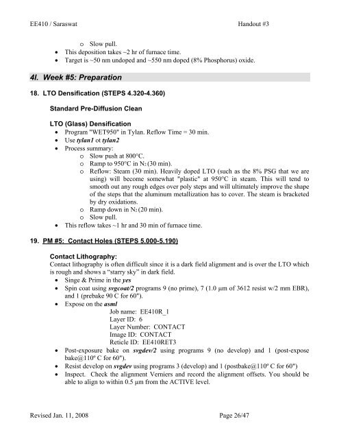
<strong>EE</strong><strong>410</strong> / <strong>Saraswat</strong> <strong>Handout</strong> <strong>#3</strong><br />
o Slow pull.<br />
• This deposition takes ~2 hr of furnace time.<br />
• Target is ~50 nm undoped and ~550 nm doped (8% Phosphorus) oxide.<br />
4I. Week #5: Preparation<br />
18. LTO Densification (STEPS 4.320-4.360)<br />
Standard Pre-Diffusion Clean<br />
LTO (Glass) Densification<br />
• Program "WET950" in Tylan. Reflow Time = 30 min.<br />
• Use tylan1 ot tylan2<br />
• Process summary:<br />
o Slow push at 800°C.<br />
o Ramp to 950°C in N2 (30 min).<br />
o Reflow: Steam (30 min). Heavily doped LTO (such as the 8% PSG that we are<br />
using) will become somewhat "plastic" at 950°C in steam. This will tend to<br />
smooth out any rough edges over poly steps and will ultimately improve the shape<br />
of the steps that the aluminum metallization has to cover. The steam is bracketed<br />
by dry oxidations.<br />
o Ramp down in N2 (20 min).<br />
o Slow pull.<br />
• This reflow takes ~1 hr and 30 min of furnace time.<br />
19. PM #5: Contact Holes (STEPS 5.000-5.190)<br />
Contact Lithography:<br />
Contact lithography is often difficult since it is a dark field alignment and is over the LTO which<br />
is rough and shows a “starry sky” in dark field.<br />
• Singe & Prime in the yes<br />
• Spin coat using svgcoat/2 programs 9 (no prime), 7 (1.0 µm of 3612 resist w/2 mm EBR),<br />
and 1 (prebake 90 C for 60").<br />
• Expose on the asml<br />
Job name: <strong>EE</strong><strong>410</strong>R_1<br />
Layer ID: 6<br />
Layer Number: CONTACT<br />
Image ID: CONTACT<br />
Reticle ID: <strong>EE</strong><strong>410</strong>RET3<br />
• Post-exposure bake on svgdev/2 using programs 9 (no develop) and 1 (post-expose<br />
bake@110º C for 60").<br />
• Resist develop on svgdev using programs 3 (develop) and 1 (postbake@110º C for 60")<br />
• Inspect. Check the alignment Verniers and record the alignment offsets. You should be<br />
able to align to within 0.5 µm from the ACTIVE level.<br />
Revised Jan. 11, 2008 Page 26/47


