

EE 410 / Saraswat Handout #3 - Stanford Nanofabrication Facility
EE 410 / Saraswat Handout #3 - Stanford Nanofabrication Facility
EE 410 / Saraswat Handout #3 - Stanford Nanofabrication Facility

You also want an ePaper? Increase the reach of your titles
YUMPU automatically turns print PDFs into web optimized ePapers that Google loves.
<strong>EE</strong><strong>410</strong> / <strong>Saraswat</strong> <strong>Handout</strong> <strong>#3</strong><br />
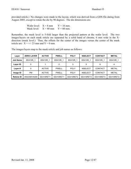
provided reticle.) No changes were made to the layout, which was derived from a GDS file dating from<br />
August 2005, except to rotate the die by 90 degrees. The die dimensions are:<br />
Wafer level: X = 8 mm Y = 16 mm.<br />
Mask level: X = 40 mm Y = 60 mm.<br />
Remember, the mask level is 5-fold larger than the projected pattern at the wafer level. The two<br />
images/layers on each mask reticle are separated by a solid band of chrome, 6 mm wide in the Xdirection<br />
(mask level.) Thus, the offsets for the center of the images versus the center of the mask<br />
reticle are: X = +/- 23 mm and Y = 0 mm.<br />
The images/layers map to the mask reticle and job names as follows:<br />
Layer ZERO LAYER ACTIVE PWELL POLY NSELECT CONTACT METAL<br />
Job Name <strong>EE</strong><strong>410</strong>R_1 <strong>EE</strong><strong>410</strong>R_1 <strong>EE</strong><strong>410</strong>R_1 <strong>EE</strong><strong>410</strong>R_1 <strong>EE</strong><strong>410</strong>R_1 <strong>EE</strong><strong>410</strong>R_1 <strong>EE</strong><strong>410</strong>R_1<br />
Layer ID 0 1 2 3 5 6 4<br />
Layer # 0 ACTIVE PWELL POLY NSELECT CONTACT METAL<br />
Image ID PM ACTIVE PWELL POLY NSELECT CONTACT METAL<br />
Reticle ID 45023981A009 <strong>EE</strong><strong>410</strong>RET1 <strong>EE</strong><strong>410</strong>RET1 <strong>EE</strong><strong>410</strong>RET2 <strong>EE</strong><strong>410</strong>RET3 <strong>EE</strong><strong>410</strong>RET3 <strong>EE</strong><strong>410</strong>RET2<br />
Revised Jan. 11, 2008 Page 12/47


