UPGRADING REPAIRING PCs
UPGRADING REPAIRING PCs UPGRADING REPAIRING PCs
24 Chapter 2—System Components and Configuration Table 2.4 Intel-Compatible Pentium-Class Processors Internal Register Data Bus Max. Processor CPU Clock Voltage Size Width Memory AMD K5 1.5–1.75x 3.5v 32-bit 64-bit 4GB AMD K6 2.5–4.5x 2.2–3.2v 32-bit 64-bit 4GB AMD K6-2 2.5–6x 1.9–2.4v 32-bit 64-bit 4GB AMD K6-3 3.5–4.5x 1.8–2.4v 32-bit 64-bit 4GB AMD Athlon 5–10x10 (nee K7) 1.6–1.8v 32-bit 64-bit 8TB AMD Athlon, 5–10x10 with performance enhancing cache (PEC) (code name “Thunderbird”) 1.8v 32-bit 64-bit 8TB AMD Duron9 6x–7.5x10 “Thunderbird” 1.6–1.8v 32-bit 64-bit 8TB Cyrix 6x86 2x 2.5–3.5v 32-bit 64-bit 4GB Cyrix 6x86MX/MII 2–3.5x 2.2–2.9v 32-bit 64-bit 4GB VIA Cyrix III 2.5–7x 2.2v 32-bit 64-bit 4GB Nexgen Nx586 2x 4v 32-bit 64-bit 4GB IDT Winchip 3–4x 3.3–3.5v 32-bit 64-bit 4GB IDT Winchip2/2A 2.33–4x 3.3–3.5v 32-bit 64-bit 4GB Rise mP6 2–3.5x 2.8v 32-bit 64-bit 4GB FPU = Floating-Point unit (internal math coprocessor) WT = Write-through cache (caches reads only) WB = Write-back cache (caches both reads and writes) Bus = Processor external bus speed (motherboard speed) Core = Processor internal core speed (CPU speed) MMX = Multimedia extensions, 57 additional instructions for graphics and sound processing 3DNow = MMX plus 21 additional instructions for graphics and sound processing SSE = Streaming SIMD (Single Instruction Multiple Data) Extensions, MMX plus 70 additional instructions for graphics and sound processing 1. The 386SL contains an integral-cache controller, but the cache memory must be provided outside the chip. 2. Intel later marketed SL Enhanced versions of the SX, DX, and DX2 processors. These processors were available in both 5v and 3.3v versions and included power-management capabilities. 3. The Enhanced mobile PII has an on-die L2 cache similar to the Celeron.
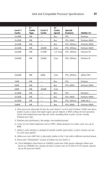
Intel and Compatible Processor Specifications 25 L1 L2 Level 1 Cache Level 2 Cache Special Cache Type Cache Speed Features Similar to4 16+8KB WB — Bus FPU Pentium 2x32KB WB — Bus FPU, MMX Pentium MMX 2x32KB WB — Bus FPU, 3DNow Pentium MMX 2x32KB WB 256KB Core FPU, 3DNow Pentium MMX 2x64KB WB 512KB6 1/37 Core FPU, 3DNow Pentium III8 2x64KB WB 256KB Core FPU, 3DNow Pentium III 2x64KB WB 64KB Core FPU, 3DNow Athlon PEC 16KB WB — Bus FPU Pentium 64KB WB — Bus FPU, MMX Pentium MMX 64KB WB 256KB Core 2x16KB WB — Bus FPU Pentium5 2x32KB WB — Bus FPU, MMX Pentium MMX 2x32KB WB — Bus FPU, 3DNow AMD K6-2 2x8KB WB — Bus FPU, MMX Pentium MMX 4. These processors physically fit into the same Socket 7 used by Intel Pentium 75MHz and above models except as noted, but might require special chipsets or BIOS settings for best operation. Check with motherboard and chip mfr. before installing them in place of your existing Pentium-class chip. 5. Pentium-class performance, but unique, non-standard pinout. 6. Cache size for initial shipments (3rd Q 1999). Athlon designed it to allow cache sizes up to 8MB. 7. Athlon’s cache interface is designed to handle variable speed ratios, so later versions can run L2 cache more quickly. 8. Athlon uses new AMD Slot A, physically similar to Slot 1 but with a different electrical pinout. 9. Duron and “Thunderbird” versions of Athlon use new Socket A. 10. Clock Multipliers listed based on 100MHz system bus (FSB) speeds; although Athlon and Duron use 200MHz bus, memory for these systems runs at PC100 or PC133 speeds, depending on the processor model.
- Page 1 and 2: UPGRADING AND REPAIRING PCs TECHNIC
- Page 3 and 4: Associate Publisher Greg Wiegand Se
- Page 5 and 6: Contents 1 General Technical Refere
- Page 7 and 8: Contents vii IDE Hard Drive Identif
- Page 9 and 10: Serial Port Configuration 172 Avoid
- Page 11 and 12: Contents xi Sound Quality Standards
- Page 13 and 14: About the Authors Scott Mueller is
- Page 15 and 16: watch, photograph, and (occasionall
- Page 17 and 18: Tell Us What You Think! As the read
- Page 19 and 20: Chapter 1 General Technical Referen
- Page 21 and 22: Understanding Bits, Nibbles, and By
- Page 23 and 24: Note Glossary of Essential Terms 5
- Page 25 and 26: Glossary of Essential Terms 7 Table
- Page 27 and 28: Glossary of Essential Terms 9 Table
- Page 29 and 30: Table 1.5 Hexadecimal/ASCII Convers
- Page 31 and 32: Hexadecimal/ASCII Conversions 13 Ta
- Page 33 and 34: Table 1.5 Hexadecimal/ASCII Convers
- Page 35: Hexadecimal/ASCII Conversions 17 Ta
- Page 38 and 39: 20 Chapter 2—System Components an
- Page 40 and 41: 22 Chapter 2—System Components an
- Page 44 and 45: 26 Chapter 2—System Components an
- Page 46 and 47: 28 Chapter 2—System Components an
- Page 48 and 49: 30 Chapter 2—System Components an
- Page 50 and 51: 32 Chapter 2—System Components an
- Page 52 and 53: 34 Chapter 2—System Components an
- Page 54 and 55: 36 Caution Chapter 2—System Compo
- Page 56 and 57: 38 Table 2.15 Troubleshooting Power
- Page 58 and 59: 40 Chapter 2—System Components an
- Page 60 and 61: 42 Chapter 2—System Components an
- Page 62 and 63: 44 modules can be divided by 9, but
- Page 64 and 65: 46 Chapter 2—System Components an
- Page 66 and 67: 48 Chapter 2—System Components an
- Page 68 and 69: 50 Other Add-On Card Configuration
- Page 70 and 71: 52 Chapter 2—System Components an
- Page 72 and 73: 54 Chapter 2—System Components an
- Page 74 and 75: 56 Chapter 2—System Components an
- Page 76 and 77: 58 Chapter 2—System Components an
- Page 78 and 79: 60 Chapter 2—System Components an
- Page 80 and 81: 62 Chapter 2—System Components an
- Page 82 and 83: 64 Chapter 2—System Components an
- Page 84 and 85: 66 Chapter 2—System Components an
- Page 87 and 88: Chapter 3 3 BIOS Configurations and
- Page 89 and 90: Where BIOS Updates Come From 71 Tab
- Page 91 and 92: How to Recover from a Failed BIOS U
Intel and Compatible Processor Specifications 25<br />
L1 L2<br />
Level 1 Cache Level 2 Cache Special<br />
Cache Type Cache Speed Features Similar to4 16+8KB WB — Bus FPU Pentium<br />
2x32KB WB — Bus FPU, MMX Pentium MMX<br />
2x32KB WB — Bus FPU, 3DNow Pentium MMX<br />
2x32KB WB 256KB Core FPU, 3DNow Pentium MMX<br />
2x64KB WB 512KB6 1/37 Core FPU, 3DNow Pentium III8 2x64KB WB 256KB Core FPU, 3DNow Pentium III<br />
2x64KB WB 64KB Core FPU, 3DNow Athlon PEC<br />
16KB WB — Bus FPU Pentium<br />
64KB WB — Bus FPU, MMX Pentium MMX<br />
64KB WB 256KB Core<br />
2x16KB WB — Bus FPU Pentium5 2x32KB WB — Bus FPU, MMX Pentium MMX<br />
2x32KB WB — Bus FPU, 3DNow AMD K6-2<br />
2x8KB WB — Bus FPU, MMX Pentium MMX<br />
4. These processors physically fit into the same Socket 7 used by Intel Pentium 75MHz and above<br />
models except as noted, but might require special chipsets or BIOS settings for best operation.<br />
Check with motherboard and chip mfr. before installing them in place of your existing<br />
Pentium-class chip.<br />
5. Pentium-class performance, but unique, non-standard pinout.<br />
6. Cache size for initial shipments (3rd Q 1999). Athlon designed it to allow cache sizes up to<br />
8MB.<br />
7. Athlon’s cache interface is designed to handle variable speed ratios, so later versions can run<br />
L2 cache more quickly.<br />
8. Athlon uses new AMD Slot A, physically similar to Slot 1 but with a different electrical pinout.<br />
9. Duron and “Thunderbird” versions of Athlon use new Socket A.<br />
10. Clock Multipliers listed based on 100MHz system bus (FSB) speeds; although Athlon and<br />
Duron use 200MHz bus, memory for these systems runs at PC100 or PC133 speeds, depending<br />
on the processor model.


