1.0 Introduction:
1.0 Introduction:
1.0 Introduction:

Create successful ePaper yourself
Turn your PDF publications into a flip-book with our unique Google optimized e-Paper software.
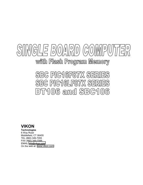
VIKON<br />
Technologies<br />
6 Way Road<br />
Middlefield, CT 06455<br />
TEL (860) 349-7055<br />
FAX (860) 349-7088<br />
EMAIL info@vikon.com<br />
On the web at: www.vikon.com
This manual applies to the the following Vikon Technologies products:<br />
Single Board Computers Assembled and Tested - SBC PIC16F872, SBC PIC16F877,<br />
SBC PIC16LF877, SBC PIC16LF876, and SBC PIC16F876.<br />
Single Board Computers Assembled and Tested with no Microcontroller or other integrated<br />
circuits - SBC 106<br />
Single Board Computers KIT – SBKIT PIC16F872 and SBKIT PIC16F877<br />
Single Board Computers KIT with no Microcontroller or other integrated circuits – SBKIT 106<br />
Single Board Computer Bare Board (no parts) - DT106<br />
Document Version – 1<br />
Revision – 2
Table of Contents<br />
<strong>1.0</strong> <strong>Introduction</strong>:.................................................................................................................. 1<br />
1.1 Features:.................................................................................................................... 1<br />
2.0 Product Variations ........................................................................................................ 2<br />
2.1 SBC PIC16F87x version differences:....................................................................... 2<br />
2.2 Manufacturing Options ............................................................................................. 2<br />
3.0 Parts List ....................................................................................................................... 3<br />
3.1 Options:..................................................................................................................... 3<br />
3.1.1 On board regulator circuit .......................................................................................... 3<br />
3.1.2 Important info when using VR1 and JP5 ....................................................................... 3<br />
3.1.3 I 2 C EEPROM Option ................................................................................................ 4<br />
3.1.4 Optional second oscillator for U1 timer 1 input: ............................................................. 4<br />
3.1.5 Optional real time clock circuit ................................................................................... 4<br />
3.1.6 Optional LCD /VFD interface..................................................................................... 4<br />
3.1.7 Optional RS-232 Serial Communications ...................................................................... 4<br />
3.1.8 Optional RS-485 Serial Communications ...................................................................... 4<br />
3.1.9 Brown-Out Circuit.................................................................................................... 4<br />
4.0 Headers and jumper info:.............................................................................................. 5<br />
5.0 IMPORTANT INFORMATION PLEASE READ:...................................................... 6<br />
5.1 In Circuit Programmers.................................................................................................... 6<br />
5.2 I 2 C Devices use C3 and C4 (RC3 & RC4 on PIC):................................................................. 6<br />
5.3 A4 (RA4) is pulled up on board using a 10K resistor.............................................................. 6<br />
5.4 Real Time Clock DS1302................................................................................................. 6<br />
6.0 Power Supply................................................................................................................7<br />
6.1 AC adapter precautions............................................................................................. 7<br />
6.2 Current requirements ....................................................................................................... 7<br />
7.0 General Information...................................................................................................... 7<br />
7.1 Handling Precautions:...................................................................................................... 7<br />
7.2 Connecting to external circuitry......................................................................................... 7<br />
7.3 Testing SBCs: ................................................................................................................ 8<br />
8.1 SimmStick Bus signals on 30 pin edge connector: ................................................................. 9<br />
8.2 LCD / VFD Header Pin Definitions: ................................................................................... 9<br />
8.3 Jumper Locations............................................................................................................ 9<br />
9.0 Compatability with In Circuit Debuggers................................................................... 10<br />
10. Software related information ...................................................................................... 11<br />
1<strong>1.0</strong> Additional Information: ............................................................................................ 14<br />
11.1 Issues with the Epic Plus Programmer ............................................................................. 14<br />
11.2 Loading and Isolation Problems with programming:........................................................... 14<br />
11.2 Using a stand alone board with a programming header:....................................................... 14
<strong>1.0</strong> <strong>Introduction</strong>:<br />
The SBC PIC16F87X series, SBC 106, and DT 106 board computer modules are based on the<br />
Microchip PICmicro PIC16F87X family of microcontrollers. Vikon Technologies offers several<br />
different variations of the module. These modules offer low cost and high performance.<br />
The modules can be used stand alone or with the SimmStick bus . They feature a SimmStick<br />
compatible edge connector.<br />
1.1 Features:<br />
• 28, and 40 pin footprints to suit all current PICmicro flash PIC1687x devices.<br />
• Alternative RS-232 or RS-485 Communications option.<br />
• Optional on board 78L05 Regulator for stand alone operation.<br />
• Optional EEProm. Same pinout as MicroChip 24LCxx family.<br />
• Optional 8570 RAM can be used as second EEProm location.<br />
• Brown out (power monitor /supervisor) integrated circuit can be installed if the user<br />
chooses to use one, the DT106 and SBC 106 can use the 40 or 28 pin older PICmicro<br />
devices that may require this circuit.<br />
• Provision for LCD 14 pin header and LCD contrast pot.<br />
• Crystal or Resonator Oscillator.<br />
• 40 pin header (40 pin dip compatible) at the top edge of the board.<br />
• Optional Dallas DS-1302 Real Time Clock.<br />
• SimmStick compatible, which means it is a Load/Run operation for Flash Micros if used in<br />
conjunction with a suitable programming platform such as the DT001.<br />
• 10 pin in circuit programming header allows various programmers (with appropriate<br />
cable) to program the PIC16F87X chips in circuit. Vikon offers the EPIC programmer with<br />
the optional cable.<br />
• PIC16F87X and PIC16LF87X offer multi channel A/D conversion up to 10 bits.<br />
1
• PIC16F87X / PIC16LF87X versions can be used as a development platform for other<br />
PICMicro parts such as the PIC16C62, PIC16C63, PIC16C64, PIC16C72, PIC16C73,<br />
PIC16C74, PIC16C774 and others (see Microchip Application Note: TB033).<br />
• Board can accept various PIC Micro parts - 28 pin and 40 pin.<br />
• Compatible with 1 to 4 line character LCD or VFD (emulator type) displays.<br />
SBC106 or DT106 Users:<br />
The Micro can be any of the flash 87x family and many other PICmicros that fit the 28 pin skinny<br />
Dip and 40 pin DIP footprints. You can even change Micro types if you install a 28 pin socket in<br />
the U5 position, and two 20 pin machine pin strips into the U1 position.<br />
2.0 Product Variations<br />
2.1 SBC PIC16F87x version differences:<br />
Microcontroller<br />
Part Number<br />
Pins Memory<br />
Flash / RAM /<br />
EEPROM<br />
Vdd<br />
range<br />
2<br />
Additional Features<br />
PIC16F872 28 2K/128/64 4-5.5V 5 ch. A/D, MSSP<br />
PIC16F877 40 8K/368/256 4-5.5V 8 ch. A/D, MSSP, USART, PSP<br />
PIC16LF876 28 8K/368/256 2.0-5.5V 5 ch. A/D, USART, MSSP, low power<br />
PIC16LF877 40 8K/368/256 2.0-5.5V 8 ch. A/D, MSSP, USART, PSP, low power<br />
PIC16F876 28 8K/368/256 4-5.5V 5 ch. A/D, USART, MSSP<br />
• LF parts are available up to 4Mhz only, F parts are available in 4 or 20Mhz versions.<br />
• For more information please consult the Microchip data sheets.<br />
2.2 Manufacturing Options<br />
The SBC PIC16F877, SBC PIC16LF876, SBC PIC16F872 and SBC PIC16LF877 are available<br />
with several manufacturing options. Depending on how you ordered the board you may have one<br />
or more of the following options.<br />
Board designated (or ordered) as “base version” boards have none of these options.<br />
Option Description of Option Notes<br />
RS232 RS232 level converter IC circuit If installed RS485 can not be<br />
installed.<br />
RS485 RS485 level converter IC If installed RS232 can not be<br />
PASSIVE232 Two resistors for a passive style RS232<br />
type interface. Not true RS232 specs.<br />
installed.<br />
Not true RS232 requires software<br />
based serial comms with inverted<br />
signals<br />
5VREG 5 Volt regulator circuit 100milliamp max only<br />
EEPROM I 2 C EEPROM 8 pin Available 512 bytes to 16K bytes<br />
EEPROM2 Second I 2 C EEPROM 8 pin Available 512 bytes to 16K bytes<br />
I 2 C-RAM I2C 8 pin RAM device Call for availability<br />
RTC Dallas Real Time Clock circuit<br />
LCD LCD 10K Pot and 14 pin header<br />
SIMMHEADER 30 pin straight or right angle header<br />
installed over edge connector.
3.0 Parts List<br />
Part designation on schematic shown in bold<br />
1. 1 X Capacitor C5 15pf – 27pf Ceramic (Depending on type & frequency of crystal)<br />
2. 1 X Capacitor C6 15pf – 27pf Ceramic (See data sheet for full details.)<br />
Note: A Crystal of a suitable value, or a 3 pin Resonator. If a crystal is fitted then C5 and C6 must be<br />
installed. If you use a Resonator, then you should not install these two caps if the resonator has internal<br />
capacitor.<br />
3. 1 X Crystal or Resonator X1 (frequency depends on board part number)<br />
4. 1 X Resistor R3 470 Ohms .25 watt<br />
Note: There is an option for a series resistor (R3) between OSC2 and the crystal. The 16F87x data<br />
sheet shows this resistor in Figure 12-2 on page 135 of the data sheet. Use a 470 ohm resistor there<br />
when running the chip in HS mode, or it will burn up the crystal very quickly. Most users should simply<br />
install the 470 Ohm resistor., Resonators and low frequency crystals may not need this resistor.<br />
5. 1 X Resistor R1 10K .25 watt<br />
6. 1 X Resistor R2 10K .25 watt Note on some SBC versions R2 may be replaced by a D2<br />
1N4148 or equivalent diode , these versions should not install a IC at U6 or the diode<br />
needs to be replaced by a 10K resistor.<br />
7. 1 X Resistor R4 10K .25 watt (installed only when a I 2 C device option installed)<br />
8. 1 X Resistor R5 10K .25 watt (installed only when a I 2 C device option installed)<br />
9. 1 X Resistor R6 10K .25 watt<br />
10. 1 X Capacitor C11 .01uf (or .1uf) Ceramic<br />
11. 1 X Capacitor C12 10uf Tantalum or Electro.<br />
12. 1 X Capacitor C13 .01uf (or .1uf) Ceramic<br />
13. 1 X Capacitor C14 .01uf (or .1uf) Ceramic<br />
3.1 Options:<br />
3.1.1 On board regulator circuit<br />
100 milliamp max:<br />
1. 1 X 780L5 +5 VR1 Voltage regulator in TO-92 case. (Optional)<br />
2. 1 X Capacitor C9 10uf Tantalum or Electro.<br />
3. 1 X Capacitor C10 .01uf (or .1uf) Ceramic<br />
Important! When using VFD displays or LED backlit LCD displays use an off board 5 volt<br />
regulator capable of handling the higher power requirements of these displays (typically<br />
greater than 300ma) !<br />
3.1.2 Important info when using VR1 and JP5<br />
JP5 is used to Isolate the +5V signal on the edge connector from the 78L05 regulator output if it<br />
is installed. Both outputs should never be used together. The track on the solder side of the board<br />
under JP5 needs to be cut to isolate the 78L05 regulator output. A test link and two male posts<br />
are used to reinstall the regulator output.<br />
Note: When running a LF part at lower voltages (below 5 volts) you may need to replace VR1<br />
with a lower voltage unit or not use VR1 at all and use an external source of regulated low voltage<br />
power.<br />
3
3.1.3 I 2 C EEPROM Option<br />
1. U4 - EEPROM 8 pin 24Cxx or 24LCxx<br />
2. U3 - EEPROM (2 nd device) or RAM options 8 pin<br />
3. 8 pin dip socket(s) 1 or two depending on options ordered<br />
4. 10K Resistors are installed at R4 and R5<br />
3.1.4 Optional second oscillator for U1 timer 1 input:<br />
1. C7 and C8 (22pf Ceramic)<br />
2. X2 32.768khz Crystal<br />
3.1.5 Optional real time clock circuit<br />
1. 1 X Dallas DS-1302 U8<br />
2. 1 X 32.768khz X3 Crystal with a load capacitance of 6pf. (For Optional DS-1302 Clock)<br />
Note: X3 may have a small 5 – 8 pf capacitor across it to compensate for crystal<br />
capacitance variations and improved timekeeping accuracy.<br />
3.1.6 Optional LCD /VFD interface<br />
1. 14 pin header<br />
2. 10K POT 1 (For Optional LCD only , not used by VFDs)<br />
3.1.7 Optional RS-232 Serial Communications<br />
1. 1 X Capacitor C1 1uf Electrolytic (PCB mount.) or Tant. @16 V.<br />
2. 1 X Capacitor C2 1uf Electrolytic (PCB mount.) or Tant. @16 V.<br />
3. 1 X Capacitor C3 1uf Electrolytic (PCB mount.) or Tant. @16 V.<br />
4. 1 X Capacitor C4 1uf Electrolytic (PCB mount.) or Tant. @16 V.<br />
5. 1 X U2 - MAX-232 or DS14C232 Integrated Circuit (or equivalent)<br />
Note the MAX232 and DS14C232 are designed for 5 volt operation, if you have a board<br />
capable of low voltage operation and intend to use it at a lower voltage, these parts will not<br />
function correctly.<br />
3.1.8 Optional RS-485 Serial Communications<br />
1 X U5 - DS75176B, MAX-485, LTC-1485 Integrated Circuit (or equivalent)<br />
Note: on boards designed for operation other than 5volts (2 – 5.5volts) such as PIC16LF87x you<br />
must use a device capable of operating at the lower voltage if you intend to operate the board at<br />
the lower voltage.<br />
Note: RS-232 and RS-485 Comms can't be installed together as the chip footprints overlap<br />
each other.<br />
3.1.9 Brown-Out Circuit<br />
Not installed or required on PIC16F87X boards:<br />
The power monitor / supervisor IC (U6) in a TO-92 package is used to stop the Micro operation<br />
becoming unpredictable during a power 'brown-out'. In most cases this isn't required. It's just an<br />
added precaution for reliable operation. The older PICmicros may well need this device. You<br />
don't need it for any PIC16F87x or PIC16LF87x chip and many of the newer PIC16C devices,<br />
consult your PICmicro data sheet for more information.<br />
4
If U6 is populated some compatible devices are Microchip MCP-120, Panasonic MN13811-S<br />
(open collector), MN1381-S (cmos), Motorola MC33064/P, Zetek ZM33064. The device should be<br />
a TO92 style package with a switching (level) voltage of 4.2 to 4.85 volts when operating at a 5<br />
volt supply. If you operate the board at lower voltages you must select a part with the appropriate<br />
voltage. Note if you must use U6 check to see if the part at R2 is a diode if it is replace with<br />
a 10K resistor.<br />
For DT106 or SBC106 users: By just simply ignoring the brown-out circuit and installing resistors<br />
R1 and R2, the circuit operation should be fine. R1, R2, and R3 must be installed at all times for<br />
normal operation. Yes, even if you don't use a brown-out circuit.<br />
4.0 Headers and jumper info:<br />
JP1:<br />
Serial Out Jumper block, default connected.<br />
JP2:<br />
Serial In Jumper block, default connected.<br />
JP1 and JP2 can easily be isolated or reversed, by cutting the tracks on the solder side of the<br />
board, and soldering in a 4 pin male header (2x2) to suit. Jumper links, or test links can be used<br />
to connect, isolate, or swap over the comms lines. The links horizontal will be the default, the<br />
links vertical will swap them over.<br />
JP3:<br />
Header block for unused gates of the MAX-232. These are spares, but can be useable if<br />
jumpered correctly for other handshaking RS-232 lines.<br />
JP4:<br />
VCC Isolate to 40 pin header J1. Default Isolated. If you wanted to run a target board from the<br />
DT106 board via J1, then it may need to have the +5V removed if it had it's own supply, as you<br />
can't have two +5V sources connected together.<br />
JP5:<br />
Used to Isolate the +5V signal on the edge connector from the 78L05 regulator output if it is<br />
installed. Both outputs should never be used together. The track on the solder side of the board<br />
under JP5 needs to be cut to isolate the 78L05 regulator output. A test link and two male posts<br />
are used to reinstall the regulator output.<br />
J1:<br />
40 pin header, pin for pin layout compatible with 40 pin Micro.<br />
Also read the notes on the J4 Programming header.<br />
J2: Real Time Clock:<br />
Used for Dallas DS-1302 to get power from a standby battery to it's VCC2.<br />
The Dallas DS-1302 (U8) requires a crystal (X3) with a load capacitance of 6pf.<br />
J3:<br />
The Real Time Clock control lines can be connected to here. Make sure you don't conflict with<br />
other signals used.<br />
J4:<br />
Programming header. Default connected through J4 on the solder side of the board.<br />
5
This header mates with J1, the 10 pin programming Header on the DT001 board, and if a 10 pin<br />
header cable is made up with flat ribbon cable, the board can be programmed via this cable. You<br />
have to cut the tracks on the solder side of the DT106 board, but make sure you don't cut the<br />
earth track (pins 9 and 10) The other 4 tracks can be cut.<br />
This allows the program/run switch on the DT001 board to be used. To return the header to a<br />
stand alone controller, 4 Test Links need to be used when the IDC crimp connector cable is<br />
removed. These must be placed across header J4, pins 1 and 2, 3 and 4, 5 and 6, and 7 and 8.<br />
This header pinout is the same as the Dr. Russ Reiss Configuration, however a suitable cable<br />
can be made up to match it with any ISP programmer.<br />
5.0 IMPORTANT INFORMATION PLEASE READ:<br />
5.1 In Circuit Programmers<br />
All programmers use pins RB7 and RB6 on the PIC (B7 & B6 on the SimmStick Bus) as well as<br />
the MCLR or reset lines. The MCLR or reset line will be brought up to a minimum of +12.5VDC to<br />
about +13.1VDC during programming. You must isolate any circuitry (including any on the<br />
SimmStick bus) that is connected to the Reset (MCLR) line or damage may occur to other<br />
circuitry or your programmer!<br />
You must also isolate B6 & B7 (RB6 & RB7) if they are being used as inputs, have a low<br />
impedance device connected to them, are connected to a bi-directional data bus (such as a LCD)<br />
or are being driven from a device output with a low impedance source, or you can not properly<br />
program the device in circuit. Best rule of thumb is to isolate them always. You can do this via J4<br />
however this does NOT isolate the SimmBus.<br />
5.2 I 2 C Devices use C3 and C4 (RC3 & RC4 on PIC):<br />
If you are using on board I 2 C EEPROM or RAM, please note that I/O lines C3 and C4 are used<br />
for this function. Any external circuitry attached to these lines may interfere with this. These lines<br />
appear on the SimmStick bus.<br />
If you are not using I 2 C devices they can be used as general I/O and they are pulled up to Vcc<br />
using 10K resistors at R4 and R5.<br />
5.3 A4 (RA4) is pulled up on board using a 10K resistor.<br />
5.4 Real Time Clock DS1302<br />
If you have a RTC IC installed at U8 it is a Dallas DS1302. You need wire the DS1302 I/O lines to<br />
your microcontroller’s I/O lines. The header J3 will need to be wired to three available I/O lines. If<br />
you plan on using battery back up , the external battery must be wired to J2.<br />
The DS1302 charges any battery attached to J2. You must use the correct type of battery or<br />
damage will occur to the battery and the circuit. Also an incorrect battery can be a safety<br />
hazard!<br />
Please read all data and application notes about the DS1302 before using! Available from<br />
Dallas Semiconductor.<br />
6
6.0 Power Supply<br />
When using this module stand alone or in a SimmStick bus, a voltage level of greater than 5 volts<br />
DC CAN NOT be applied to pin 7 of the SimmStick edge connector or if you are powering from<br />
pin 21 of J1!<br />
Power supplies must be regulated and filtered for proper operation. Unregulated and unfiltered<br />
power sources may damage the unit and provide unreliable operation, they will also violate any<br />
warranty!<br />
6.1 AC adapter precautions<br />
DO NOT USE AN AC ADAPTER OR POWER SUPPLY THAT PROVIDES NO<br />
AC POWER LINE ISOLATION – YOU MUST USE A TRANSFORMER TYPE<br />
UNIT THAT IS UL AND / OR CSA APPROVED! YOUR POWER SOURCE<br />
MUST BE ISOLATED FROM THE AC LINE.<br />
WHEN USING AC ADAPTORS - THE AC POWER ADAPTOR UNIT SHOULD BE MARKED:<br />
CLASS 2 TRANSFORMER or PLUG IN CLASS 2 TRANSFORMER. Failure to comply with<br />
this requirement may cause a unsafe or hazardous condition to occur!<br />
6.2 Current requirements<br />
The amount of current (power) depends on what options are installed on your board and what<br />
types of devices are being driven by the board (i.e. LEDS, LCD display etc…) The speed of the<br />
board will also determine some of the power requirements, example a 20Mhz clocked PIC<br />
requires more power than a 4Mhz clocked PIC.<br />
Consult device data sheets for power requirements.<br />
Typically a SBC PIC16F87X series module running at 20 Mhz requires less than 80 milliamps<br />
with most options and a LCD (no backlight power) attached.<br />
7.0 General Information<br />
7.1 Handling Precautions:<br />
When working with a circuit board please take normal anti-static handling procedure precautions.<br />
Keep unused boards in antistatic bags or packaging. Use antistatic mats or other devices at your<br />
workstation to reduce the chance of static electricity from your body discharging into the board.<br />
Always remove power when installing a board into a circuit or a SimmStick bus backplane.<br />
Always remove power when attaching or removing devices connected to any of the headers on<br />
the board.<br />
7.2 Connecting to external circuitry<br />
The I/O pins of the SBC module are connected directly to the PIC microcontroller with the<br />
exception of the RS232 and RS485 which are connected to level converter chips.<br />
Care should be taken that the maximum voltage for an input is not exceeded. Typically you<br />
should not drive an input greater than 5 volts (or the VDD supply) or go below ground (negative<br />
voltage). If the signal may exceed these limits a resistor should be placed in series with the input.<br />
This resistor should be high enough in value to limit the current that will flow through the input<br />
7
protection diodes on the PIC. How ever if the voltage is to high you may need some type of<br />
interface circuit. Also you may need optically coupled inputs for safety or isolation purposes.<br />
When using the PIC I/O as an output, it can sink or source up to 25 milliamps per output. When<br />
supplying multiple outputs at high current levels care must be taken the maximum chip power<br />
dissipation is not exceeded and the maximum combined current output is 200 milliamps.<br />
Consider using buffer ICs capable of supplying high currents such as ULN2803 / ULN2804 or<br />
ULN2003.<br />
When using the analog inputs of the analog to digital converter , noise on the analog input or Vref<br />
can affect conversion accuracy. If you are using VDD /VSS as Vref , noise on the power supply<br />
can be a factor.<br />
The PIC oscillator should not be used to drive other circuitry. If you want to drive multiple device<br />
with the same clock, use an external clock circuit to drive the PIC and the other devices. When<br />
using external clocks, remove the crystal or resonator and any associated capacitors.<br />
Finally if external signal sources are being used to supply counter, timer inputs, or interrupts you<br />
must make certain noise and glitches will not affect circuit operation. Short glitches or spikes can<br />
false trigger PIC’s internal circuitry.<br />
7.3 Testing SBCs:<br />
When ever you attach test equipment make sure you understand the loading of the equipment on<br />
the circuit (both from a DC and AC stand point). Be careful where you attach test equipment<br />
grounds. Always use proper probes and leads for your equipment.<br />
Please note that capacitive loading effects of a scope, frequency counter, logic analyzer, or meter<br />
test lead or probe when probing the PIC oscillator circuit can cause the crystal or resonator to<br />
stop oscillating or shift its operating frequency. In fact even a 10 to1 100Mhz probe with about<br />
14pf input cap. can cause a 20Mhz crystal on a PIC to shut down or not start up.<br />
Note when debugging with a scope, the PIC timer / counter inputs can miss trigger on short (fast)<br />
glitches that your equipment may not properly display. Even when your source is a slow pulse a<br />
fast glitch from some outside interference can cause this problem.<br />
Ground loops are source of many problems when connecting external signals, they may be<br />
further enhanced by test equipment grounding introduced into the circuit.<br />
8
8.0 Pinouts and Jumper Locations<br />
8.1 SimmStick Bus signals on 30 pin edge connector:<br />
Pin Description Pin Description Pin Description<br />
1 Serial Out 11 C4 and I 2 C SDA 21 B6<br />
2 Serial In 12 C7 / SI 22 B7<br />
3 N/C 13 C6 /SO 23 A0<br />
4 +VDC In Unregulated 14 C5 24 A1<br />
5 N/C 15 B0 25 A2<br />
6 N/C 16 B1 26 A3<br />
7 VDD power in<br />
(regulated +5VDC)<br />
17 B2 27 A4<br />
8 Reset (MCLR) 18 B3 28 A5<br />
9 Ground 19 B4 29 C2<br />
10 C3 and I 2 C SCL 20 B5 30 C3<br />
8.2 LCD / VFD Header Pin Definitions:<br />
Pin Micro – LCD Pin Micro - LCD Pin Micro - LCD<br />
1 - Ground 6 B3 - Enable 11 B4 – Data 4<br />
2 - Vcc 7 N/C 12 B5 – Data 6<br />
3 - Contrast Pot 8 N/C 13 B6 – Data 7<br />
4 B1 – R/S 9 N/C 14 B7 – Data 8<br />
5 B2 – Read/Write 10 N/C 15/16 N/C<br />
8.3 Jumper Locations<br />
9
9.0 Compatability with In Circuit Debuggers<br />
The SBC PIC16F87X , DT106, and SBC106 are compatible with various in circuit debuggers.<br />
Vikon Technologies offers the PIC-ICD. Both 28 pin and 40 pin versions can be debugged with<br />
the PIC-ICD. The PIC-ICD is an improved version of the MPLAB ICD and is fully compatible<br />
with Microchip’s MBLAB software. Therefore you get all the same debugging capability (plus<br />
more) as you do with the MBLAB ICD.<br />
The Microchip MPLAB ICD can also be used with these boards. Vikon supports these boards with<br />
the MPLAB ICD and has tested the boards with it. The following limitations have been observed.<br />
The following resources are not available when using the MPLAB ICD (or PIC-ICD), I/O pins RB6<br />
and RB7, MCLR (reset) , low voltage ICSP is disabled, one stack level is used, last 288 words of<br />
program memory is used, 6 file registers are used, and the first program memory location must<br />
be a NOP.<br />
Your circuits can not make use of RB6 and RB7 when the MPLAB ICD is used. Because the<br />
onboard LCD header uses these as Data pins to the LCD or VFD display the on board LCD<br />
header can not be used when the MPLAB ICD is being used.<br />
We have also observed that the in-circuit module can cause the PIC oscillator not to start<br />
properly when inserted into a SBC with a 20 Mhz crystal (in fact any crystals above 4Mhz<br />
may exhibit this). The 4Mhz versions appear to work properly. The fix may be to reduce the<br />
values of the C5 and C6 capacitors to about 10pf Or remove the crystal and capacitors C5 /C6<br />
and drive the PIC with a Crystal oscillator. The PIC-ICD has the ability to use a Oscillator you<br />
install on it and then set the PIC-ICD jumper to use it, in this case you do not have to<br />
modify your circuit.<br />
If U6 the on board power supervisor IC is installed it will not work with the MPLAB ICD.<br />
Please read the manual that was supplied with MPLAB ICD or PIC-ICD to understand the<br />
limitations.<br />
When using PIC BASIC Pro with either the MPLAB ICD or the PIC-ICD be sure to include<br />
the ICDDEFS.BAS file in your program:<br />
Include “ICDDEFS.BAS”<br />
When developing programs using Microchip’s assembler MPASM please follow the information<br />
and limitations as outlined in the PIC-ICD or MBLAB ICD manuals for proper operation with<br />
assembler generated code and the SBC PIC16F87X / DT106 / SBC106 products.<br />
10
10. Software related information<br />
You should always refer to the proper Microchip data sheet to obtain all the information about the<br />
device’s register layout and on board modules. Microchip also publishes application notes which<br />
may help you in understanding on how to use PICmicro devices.<br />
The serial I/O is located on RC6 - transmit data and RC7 - receive data. These are the pins used<br />
with the hardware’s USART. On PIC16F872 based boards there is no USART but you can use<br />
software based UART routines similar to other PIC devices (such as the PIC16F84). Of course<br />
you can use software UART even on devices with the hardware USART.<br />
For RS485 applications the data direction line is controlled by RB0. The board supports half<br />
duplex two wire only. The RS485 data lines are the same as above.<br />
PIC Basic Pro software based serial I/O work fine, just make sure you specify the correct port<br />
pins. In addition PIC Basic Pro supports hardware serial I/O on all except the PIC16F872 parts.<br />
When using standard PIC Basic (not the PRO version) only software base serial I/O is supported<br />
and only on Port B. You can of course access the hardware registers of the USART directly in<br />
PIC Basic or write an assembly routine and call it from PIC Basic.<br />
The I 2 C signals are located at Port C , RC3 is SCL (clock) and RC4 is SDA (data). All the<br />
PIC16F87X family devices feature a hardware MSSP module that supports I 2 C communications<br />
using hardware. Pic Basic and Pic Basic Pro feature a software I 2 C approach and do not use the<br />
MSSP. You can access the MSSP registers directly from PIC Basic or PIC Basic Pro and write<br />
your own routines to access the I 2 C bus. If you decide to use the software based routines in PIC<br />
Basic and Pro , make sure you specify the correct port and pin. In Pic Basic you modify an<br />
include file, in Pic Basic Pro it is specified as part of the command.<br />
The LCD header is directly accessible from PIC Basic Pro’s LCD routines but you must specify<br />
the correct DEFINEs in your program. Example PIC BASIC PRO code snippet below:<br />
DEFINE OSC 4 ‘4 Mhz oscillator<br />
’Define ports on SBC PIC16F87X , DT106 or SBC 106:<br />
DEFINE LCD_DREG PORTB<br />
DEFINE LCD_DBIT 4<br />
DEFINE LCD_RSREG PORTB<br />
DEFINE LCD_RSBIT 1<br />
DEFINE LCD_EREG PORTB<br />
DEFINE LCD_EBIT 3<br />
DEFINE LCD_BITS 4<br />
DEFINE LCD_LINES 2 ‘for two line displays<br />
DEFINE LCD_RWREG PORTB<br />
DEFINE LCD_RWBIT 2<br />
DEFINE LCD_COMMANDUS 2000<br />
DEFINE LCD_DATAUS 50<br />
pause 200 ‘wait about 200 milliseconds for LCD to initialize internally<br />
Lcdout $fe,1,$fe,2, "TEST PROGRAM"<br />
PIC Basic (not the Pro version) does not have LCD functions built in, but you can still access the<br />
LCD from a PIC Basic program:<br />
11
'PIC Basic (for non Pro version) LCD 2 line Display Test<br />
Symbol PortLCD = 6<br />
Symbol TrisB = $86<br />
Symbol Lcde = 3<br />
Symbol Rs = 1<br />
Symbol Rw = 2<br />
poke trisb,0<br />
low lcde<br />
low rw<br />
gosub lcdinit<br />
gosub lcdclr<br />
gosub lcdhome<br />
For B4 = 0 to 17 'send string to lcd one letter at a time<br />
Lookup B4,("VIKON TECHNOLOGIES"),B2 'get letter from string<br />
Gosub lcddata 'send letter in B2 to lcd<br />
Next B4<br />
b2=$c0 'second line<br />
gosub lcdcom<br />
For B4 = 0 to 19 'send string to lcd one letter at a time<br />
Lookup B4,("DISPLAY TEST PROGRAM"),B2 'get letter from string<br />
Gosub lcddata 'send letter in B2 to lcd<br />
Next B4<br />
End<br />
'===============================================================<br />
'SUBS<br />
' subroutine to initialize the lcd - uses B2 and B3<br />
lcdinit:<br />
Pause 15 'wait at least 15ms<br />
Poke PortLCD,$30 ' 3 shifted up initialize the lcd<br />
gosub lcdtog 'toggle the lcd enable line<br />
Pause 5 'wait at least 4.1ms<br />
Poke PortLCD,$30 'initialize the lcd<br />
gosub lcdtog 'toggle the lcd enable line<br />
Pause 1 'wait at least 100us<br />
Poke PortLCD,$30 'initialize the lcd<br />
gosub lcdtog 'toggle the lcd enable line<br />
Pause 1 'wait once more<br />
Poke PortLCD,$20 'put lcd into 4 bit mode<br />
gosub lcdtog 'toggle the lcd enable line<br />
B2 = $28 '4 bit mode, 2 lines, 5x7 font<br />
Gosub lcdcom 'send B2 to lcd<br />
B2 = $0c 'lcd display on, no cursor, no blink<br />
Gosub lcdcom 'send B2 to lcd<br />
B2 = $06 'lcd entry mode set, increment, no shift<br />
Goto lcdcom 'exit through send lcd command<br />
12
' subroutine to clear the lcd screen - uses B2 and B3<br />
lcdclr: B2 = 1 'set B2 to clear command and fall through to lcdcom<br />
goto lcdcomp:<br />
' return cursor home<br />
lcdhome: B2 = 2<br />
lcdcomp:<br />
gosub lcdcom<br />
pause 1<br />
return<br />
'COMMAND<br />
' subroutine to send a command to the lcd - uses B2 and B3<br />
lcdcom:<br />
B3 = B2 & $f0 'isolate top 4 bits<br />
Poke PortLCD,B3 'send top 4 bits to lcd<br />
gosub lcdtog 'toggle the lcd enable line<br />
B3 = B2 * 16 'shift bits up to B4-B7<br />
B3 = B3 & $f0<br />
Poke PortLCD,B3 'send 4 bits to lcd<br />
gosub lcdtog 'toggle the lcd enable line<br />
Pause 1 'wait 1ms for write to complete<br />
Return<br />
' subroutine to send data to the lcd - uses B2 and B3<br />
lcddata:<br />
low rw<br />
B3 = B2 & $f0 'isolate top 4 bits<br />
B3 = B3 + 2 'add in register select to indicate data<br />
Poke PortLCD,B3 'send upper 4 bits to lcd<br />
gosub lcdtog 'toggle the lcd enable line<br />
B3 = B2 * 16 'shift bits up to B4-B7<br />
B3 = B3 & $f0<br />
B3 = B3 + 2 'add in register select to indicate data<br />
Poke PortLCD,B3 'send lower 4 bits to lcd<br />
gosub lcdtog 'toggle the lcd enable line<br />
Pause 1 'wait 1ms for write to complete<br />
Return<br />
' subroutine to toggle the lcd enable line<br />
lcdtog:<br />
High Lcde 'set lcd enable line high<br />
Low Lcde 'set lcd enable line low<br />
Return<br />
13
1<strong>1.0</strong> Additional Information:<br />
11.1 Issues with the Epic Plus Programmer<br />
The EPIC Plus programmer is compatible with the SBCPIC16F87X SBC with the proper cable.<br />
If you purchased a bundle from Vikon Technologies with the EPIC Plus programmer and a<br />
SBCPIC16F87X you are supplied this cable. The cable attaches the EPIC Plus programming<br />
header to the J4 programming header on the SBC board. Note this is not a straight through cable<br />
and requires a custom cable.<br />
The EPIC Plus should only be attached when both its power and the SBC boards power is off.<br />
When the EPIC Plus is attached the SBC may not reset and run, you must remove the<br />
programming cable to free up the reset line. Also note that RB6 and RB7 on the PIC are the<br />
programming pins, if these bus signals have a low impedance source on them during<br />
programming you will get programming errors. These pins are brought out to the SimmStick bus<br />
and are used by the LCD. Both of which are a potential source of interference with programming.<br />
If you are not using the bi-directional bus capability of the LCD display, you should wire its R/W<br />
line so that the LCD bus will always in the write mode and not read, this helps in some situations.<br />
You can also try isolation resistors on RB6 and RB7 such that they are in series with your circuitry<br />
(if this does not affect your circuit performance or function). The programming line would connect<br />
directly to the pins on the PIC. Try values from 22K to 33K ohms. If all else fails you will need to<br />
isolate RB6 and RB7.<br />
Vikon Technologies offers an optional switched cable to help isolate RB7, RB6 and Reset lines<br />
during programming (contact Vikon or your dealer for more information and pricing). This requires<br />
modifying the board by cutting the circuit traces beneath J4 on pins 4-3, 6-5, and 8-7. When the<br />
switched cable is not in use, jumpers need to be placed on J4 pins 4-3, 6-5 and 8-7 for proper<br />
operation.<br />
11.2 Loading and Isolation Problems with programming:<br />
Using Slot one of the DT001 board:<br />
The SBCPIC16F87X / DT106 / SBC106 will program in much the same manner as the DT101<br />
using an 84, however there are some conflicts.<br />
As you have only 30 pins on the Simm Bus, some signals will be missing between the slot 1<br />
DT106, and slots 2 to 7.<br />
These would need to be manually jumpered from perhaps the J1 header to a second DT106<br />
board, if the full signals need to be transferred between SimmSticks.<br />
As the board has provision for peripherals on RB6 and RB7, which are programming pins, you<br />
would either need to remove these devices (LCD and JI I/O), or use the programming header<br />
principle.<br />
For instance, you could put the DT106 into Slot 2, install the programming header between the<br />
DT001 and DT106 board, remember to cut the correct tracks on the solder side of the DT106<br />
board, and you have full isolation of the LCD and J1 header.<br />
11.2 Using a stand alone board with a programming header:<br />
You install the header cable, cut the tracks so you have full isolation. You can then connect a 40<br />
14
wire header cable (on the solder side of the board) off to your target system. This can be any 87x<br />
target board. You just pop the 40 pin header into your board. Depending on VCC requirements,<br />
you may choose to use JP4 to isolate or extend the power to the target board.<br />
28 pin Skinny Dip:<br />
OK, there is no way you are going to get this matching up via a 40 pin header system, but it's not<br />
that hard to do.<br />
1) Crimp a special cable.<br />
2) Use a small proto board to give you a 40 pin input to a 28 pin output with male header pins,<br />
and 28 wires. and use crimp connectors in and out.<br />
15