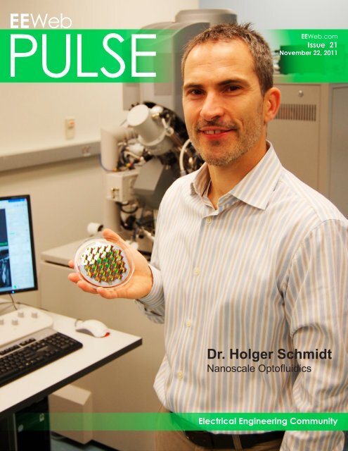
Dr. Holger Schmidt - EEWeb
Dr. Holger Schmidt - EEWeb
Dr. Holger Schmidt - EEWeb

Create successful ePaper yourself
Turn your PDF publications into a flip-book with our unique Google optimized e-Paper software.
<strong>EEWeb</strong><br />
PULSE<br />
<strong>EEWeb</strong>.com<br />
Issue 21<br />
November 22, 2011<br />
<strong>Dr</strong>. <strong>Holger</strong> <strong>Schmidt</strong><br />
Nanoscale Optofluidics<br />
Electrical Engineering Community
It’s all about<br />
connections. <strong>EEWeb</strong><br />
Electrical Engineering Community<br />
engineers<br />
hobbyists<br />
discussions<br />
power<br />
microcontroller<br />
Digi-Key is an authorized distributor for all supplier partners. New products added daily.<br />
© 2011 Digi-Key Corporation, 701 Brooks Ave. South, Thief River Falls, MN 56701, USA<br />
Contact Us For Advertising Opportunities<br />
The user-to-user forum is for everyone, from<br />
design engineers to hobbyists, to discuss<br />
technology, products, designs and more.<br />
Join the discussions that match your interest<br />
or offer your expertise to others.<br />
Join the discussion now at:<br />
students<br />
industry experts<br />
1.800.574.2791<br />
advertising@eeweb.com<br />
www.eeweb.com/advertising<br />
community<br />
wireless<br />
www.digikey.com/techxchange<br />
technical documents<br />
lighting<br />
sensor<br />
resources<br />
application notes<br />
white papers<br />
links<br />
reference designs
TABLE OF CONTENTS<br />
<strong>Dr</strong>. <strong>Holger</strong> <strong>Schmidt</strong> 4<br />
DIRECTOR, W.M. KECK CENTER FOR NANOSCALE OPTOFLUIDICS<br />
Interview with <strong>Dr</strong>. <strong>Holger</strong> <strong>Schmidt</strong> - Professor of Electrical Engineering, UC Santa Cruz.<br />
Single Molecules on a Chip 7<br />
BY HOLGER SCHMIDT<br />
Exploring chip-scale integration of nanotechnology and integrated optics for biomolecular<br />
science.<br />
Featured Products 10<br />
Tradeoffs in New Generation ADCs 12<br />
BY ED KOHLER AND JASON MESSIER WITH INTERSIL<br />
Analog-to-Digital Converters are becoming increasingly pervasive, and Kohler and Messier<br />
offer critical tradeoffs for product design success.<br />
Hey You, Get Into My Cloud 19<br />
BY ROB IRWIN WITH ALTIUM<br />
How web-based services will change the future of the electronic design process.<br />
RTZ - Return to Zero Comic 24<br />
<strong>EEWeb</strong> | Electrical Engineering Community Visit www.eeweb.com 3<br />
TABLE OF CONTENTS
INTERVIEW<br />
<strong>Dr</strong>. <strong>Holger</strong> <strong>Schmidt</strong><br />
W.M. Keck Center for Nanoscale Optofluidics<br />
How did you get into<br />
engineering and when did you<br />
start?<br />
My original degree is in physics.<br />
My M.S. thesis project dealt with<br />
semiconductor devices with<br />
direct applications in fiber-optic<br />
communications. After my PhD<br />
work in Electrical Engineering on a<br />
similar topic, I decided to develop<br />
new optical devices and methods<br />
with real-world applications.<br />
What are your favorite<br />
hardware tools that you use?<br />
I enjoy working with a variety of<br />
lasers, in particular ultrafast lasers<br />
that produce short optical pulses<br />
only about 100 femtoseconds long.<br />
With these lasers, we can study<br />
materials on time scales that cannot<br />
be reached electronically. We also<br />
have recently set up a dual beam<br />
electron/ion beam microscope in<br />
our W.M. Keck Center for Nanoscale<br />
Optofluidics. An optofluidic device<br />
combines integrated optics with<br />
microfluidics. This can be a<br />
fluidically tuneable optical device,<br />
for example a fluidic dye laser, in<br />
which the active laser dye solution<br />
is contained in a microchannel on<br />
a chip. It can also be a device that<br />
uses integrated optical elements<br />
(waveguides, filters, splitters) to<br />
investigate or manipulate particles<br />
in a microfluidic channel, for<br />
example an integrated biosensor.<br />
<strong>Dr</strong>. <strong>Holger</strong> <strong>Schmidt</strong> - Professor of Electrical Engineering; UC Santa Cruz<br />
This is an extremely versatile nanofabrication<br />
and nanocharacterization<br />
tool that is a lot of fun to work<br />
with and allows us to both sculpt and<br />
image objects on the nanoscale.<br />
What are your favorite<br />
software tools that you use?<br />
I mostly work with MATLAB,<br />
do some programming in C,<br />
and design optical waveguide<br />
structures using simulation<br />
packages from Photon Design.<br />
What is on your bookshelf?<br />
I have recently read The Master<br />
Switch: The Rise and Fall of<br />
Information Empires by Tim Wu<br />
which deals with the fascinating<br />
story of the people and companies<br />
that invented new communication<br />
technologies and how they deal<br />
with issues of information control.<br />
The Elegant Universe by Brian<br />
Greene also tells a great story<br />
on the cosmic scale, presenting<br />
an introduction to string theory<br />
and its implications. I also read<br />
contemporary and classic fiction,<br />
plus a lot of children’s books with<br />
my family. Most recently, I read<br />
Aaron Hawkins’ The Year Money<br />
Grew on Trees which tells a great<br />
coming-of-age story that shows<br />
how hard work, persistence,<br />
and a great group of friends can<br />
accomplish almost anything.<br />
<strong>EEWeb</strong> | Electrical Engineering Community Visit www.eeweb.com 4<br />
FEATURED INTERVIEW
INTERVIEW<br />
Do you have any tricks up<br />
your sleeve?<br />
In my view, the keys to achieving<br />
breakthroughs in the lab are a<br />
combination of good planning<br />
ahead of time, persistence, the<br />
ability to recognize problems or<br />
new directions, and a bit of luck at<br />
the right time.<br />
We need to stay<br />
one step ahead by<br />
providing cuttingedge<br />
training to<br />
our bright and<br />
motivated students.<br />
What has been your favorite<br />
project?<br />
For a number of years, I have had the<br />
vision of realizing optical quantum<br />
interference effects on a chip.<br />
Quantum coherence produces<br />
strange effects such as making<br />
opaque materials transparent,<br />
slowing light down, or making<br />
single photons “talk to each other.”<br />
Possible applications for quantum<br />
coherence devices include alloptical<br />
nonlinear devices (e.g.,<br />
switches) that work on the few to<br />
single photon level, optical storage<br />
and memory, extremely sensitive<br />
metrology devices (magnetometers,<br />
interferometer), or single photon<br />
light sources and detectors.<br />
In collaboration with our colleagues<br />
at BYU, we have recently succeeded<br />
in slowing light down over a 1,000<br />
times on a tiny silicon chip. Viewed<br />
differently, we have taken a 20 foot<br />
long optical pulse and compressed<br />
it to a fraction of an inch on a chip.<br />
Do you have any note-worthy<br />
engineering experiences?<br />
Being exposed to a one million<br />
volt spark from a Tesla coil (http://<br />
photon.soe.ucsc.edu/classes.htm )<br />
while standing in a metal suit that<br />
acted as a Faraday cage and NOT<br />
getting shocked was one of the<br />
most exhilarating experiences of my<br />
teaching career.<br />
What are you currently<br />
working on?<br />
We’re using laser optics in a<br />
number of ways. We are studying<br />
nanomagnets for next-generation<br />
data storage media, will attempt<br />
to stop light on a chip to create<br />
optical memory devices, and are<br />
developing optofluidic chips for<br />
biomolecular diagnostics such as<br />
virus detection at the point of care.<br />
We use different methods to make<br />
the magnets. We make our own<br />
magnets using electron beam<br />
lithography. A photoresist is<br />
patterned with nanoscale holes;<br />
magnetic material (e.g., nickel)<br />
is deposited, followed by a liftoff<br />
process. We also get samples<br />
from Western Digital, San Jose,<br />
formerly Hitachi Global Storage<br />
Technologies. These are metallic<br />
multilayers deposited on nanosize<br />
islands that were etched into a<br />
substrate wafer. Finally, we work<br />
with a group at the University of<br />
Chemnitz, Germany, which deposits<br />
magnetic layers on top of selfassembled<br />
silica nanospheres. The<br />
spheres produce ordered patterns<br />
as they are spread on a wafer which<br />
can make for a very quick and<br />
inexpensive patterning step. The<br />
main application we are interested<br />
in at the moment is bit-patterned<br />
magnetic storage media for nextgeneration<br />
hard drives. However,<br />
nanomagnets are also relevant for<br />
memory devices (MRAM) or other<br />
emerging spintronic applications.<br />
What direction do you see<br />
your business heading in the<br />
next few years?<br />
I see a lot of potential in optofluidic<br />
technology—the combination of<br />
microfluidics and integrated optics.<br />
It allows us to look at devices that<br />
have been used for optoelectronic<br />
and communication applications<br />
in a new light. Their combination<br />
with non-solid media such as gases<br />
and liquids poses new research<br />
questions, but also has a lot of<br />
applications in the life sciences,<br />
biomedicine, toxicology, pollution<br />
monitoring, and other fields.<br />
What challenges do you<br />
foresee in our industry?<br />
We need to stay one step ahead,<br />
which will provide cutting-edge<br />
training to our bright and motivated<br />
students. ■<br />
<strong>EEWeb</strong> | Electrical Engineering Community Visit www.eeweb.com 5<br />
FEATURED INTERVIEW
New Encoder for the<br />
Worst Case Environments<br />
Avago Technologies new AEAT-6600<br />
Hall E ect Magnetic Encoder delivers optimal<br />
solutions for Robotic, Industrial and Medical<br />
systems designers.<br />
• World’s highest resolution<br />
• 16-bit absolute positiion through SSI<br />
• Programmable Magnetic Rotary Encoder IC<br />
• 16-pin TSSOP package<br />
• Power down mode<br />
Avago Technologies Motion Control Products<br />
For more information and to request<br />
a free sample go to:<br />
www.avagotech.com/motioncontrol
PROJECT<br />
S ingle<br />
Molecules<br />
on a Chip<br />
The history of integrated photonics dates back to the<br />
late 1960s when researchers at Bell Labs proposed<br />
the use of thin film technology to create planar optical<br />
structures that would mimic the successful integration<br />
paradigm of integrated electronic circuits. The field<br />
grew rapidly along with the burgeoning area of fiberoptic<br />
communications. Even though early approaches<br />
to long-haul fiber links considered liquid-filled fibers,<br />
integrated optics was implemented almost exclusively<br />
in solid-state materials due to the challenges of guiding<br />
light through substances with low refractive indices<br />
such as gases and liquids. Unfortunately, this has<br />
prevented the creation of integrated optical devices<br />
and systems for a large class of areas, in particular the<br />
life sciences for which fluids (air, water) are the natural<br />
environment. It has only been over the past few years<br />
that rapid advances in microfluidics, silicon photonics,<br />
and integrated optics have converged into the new,<br />
burgeoning field of optofluidics, the combination of<br />
integrated optics and fluidics in a single system.<br />
The groups of <strong>Holger</strong> <strong>Schmidt</strong> at UC Santa Cruz<br />
and Aaron Hawkins at Brigham Young University<br />
have developed a unique approach to optofluidics<br />
that is based on creating micron-scale channels that<br />
simultaneously guide light and liquids on a silicon chip.<br />
By <strong>Dr</strong>. <strong>Holger</strong> <strong>Schmidt</strong><br />
The combination of these “liquid-core waveguides”<br />
with more conventional solid-state structures creates<br />
fully self-contained, planar chips that allow for the study<br />
and manipulation of fluids and particles therein with<br />
the convenience of off-the-shelf fiber optics equipment.<br />
Much of the early work focused on exploration of basic<br />
photonic properties such as low-loss light propagation,<br />
optical mode structure, and implementation of optical<br />
signal processing such as spectral filtering in the<br />
liquid-core waveguides. The greatest potential of the<br />
technology, however, lies in the application of these<br />
devices to fields that historically were off limits for<br />
integrated optics, for example molecular biology,<br />
medical diagnostics, toxicology, or gas spectroscopy. In<br />
particular, the demonstration of optical detection of single<br />
fluorescent molecules showed a sensitivity normally<br />
seen in expensive and bulky microscopy equipment,<br />
and provided much stimulation for new research and<br />
applications dealing with single particles on a chip.<br />
To this end, the W.M. Keck Foundation supported the<br />
creation of the Center for Nanoscale Optofluidics at<br />
UC Santa Cruz. Directed by Professor <strong>Holger</strong> <strong>Schmidt</strong>,<br />
the Center brings together faculty from five different<br />
departments (H. Noller, Molecular Biology; M. Akeson<br />
and D. Deamer, Biomolecular Engineering; J. Zhang,<br />
<strong>EEWeb</strong> | Electrical Engineering Community Visit www.eeweb.com 7<br />
FEATURED PROJECT
PROJECT<br />
single-mode fiber<br />
Figure 1: Cartoon of optofluidic chip; photograph of chip during experiment; scanning electron images of<br />
Waveguide cross sections with hollow and solid cores along with guided light mode.<br />
Chemistry; and W. Dunbar, Computer Engineering).<br />
In this Center, the researchers are able to take an<br />
interdisciplinary approach to exploring the use of<br />
nanoscale elements in conjunction with optofluidic<br />
waveguides to address problems in molecular biology,<br />
biophysics, and medical diagnostics.<br />
One focus area of research within the Center is the<br />
incorporation of nanopores into optofluidic devices.<br />
The concept of nanopore biophysics was proposed by<br />
D. Deamer who recognized that a molecule passing<br />
through a nanoscale hole in a membrane could partially<br />
block the opening, and therefore reduce the amount<br />
of electric (ionic) current flowing through that hole.<br />
Effectively, such a structure functions as an electric,<br />
single molecule detector that can distinguish molecular<br />
signatures on the picoampere level. Recently, the groups<br />
of Professors <strong>Schmidt</strong> and Noller have demonstrated the<br />
first detection of single ribosomes using nanopores that<br />
were incorporated into a dielectric layer that comprises<br />
the liquid-core optofluidic waveguide. Moreover, they<br />
multi-mode fiber<br />
were able to control the amount of nanoparticles that<br />
entered the fluidic channel by changing the applied<br />
electrical voltage. This opens up the possibility to use<br />
the nanopores as “smart gates” to introduce individual<br />
fluorescent particles into the liquid-core waveguides<br />
where they can then be investigated “on demand.”<br />
Additional collaborations are under way to apply this<br />
principle to quantum dot labeled DNA for genetic<br />
analysis and controlled nanopore translocation for DNA<br />
sequencing.<br />
Another focus area of the Center expands on the theme<br />
of particle control. Professor <strong>Schmidt</strong>’s group has<br />
recently developed new implementations of optical<br />
particle trapping (i.e., the control over a particle’s motion<br />
and position using optical forces). Using the intrinsic<br />
optical properties of the liquid-core waveguides, they<br />
were able to hold particles in place at any position along<br />
the fluidic channel. In addition, they used light beams<br />
to accumulate over 100 particles at a single spot within<br />
the waveguide, effectively creating the equivalent of an<br />
<strong>EEWeb</strong> | Electrical Engineering Community Visit www.eeweb.com 8<br />
FEATURED PROJECT
PROJECT<br />
Figure 2: Cut-open views of waveguide intersection<br />
with fluorescent particles (green) in light beam (red).<br />
optical leaf blower. Current efforts are directed at using<br />
optical forces to create optofluidic devices for particle<br />
sorting as well as to examine new trapping paradigms<br />
and the potential of moving particles between welldefined<br />
chemical microenvironments.<br />
A third thrust area deals with single molecule<br />
Figure 3: Optofludic waveguide chip with nanopore. Applied voltage is used<br />
to drive nanoparticles through Nanopore into fludic channel.<br />
spectroscopy for biomedical applications. The<br />
demonstrated ability to detect fluorescent signatures<br />
from single molecules opens up the possibility to<br />
observe and count individual, labeled bioparticles<br />
such as nucleic acids (DNA, RNA) and proteins. These<br />
play a central role in molecular diagnostics applied to<br />
infectious disease detection, genetic screening, and<br />
genomics-based personalized medicine. The ability<br />
to identify single molecules on an integrated platform<br />
has the potential to break with the current diagnostic<br />
paradigm of amplifying the genomic material to create<br />
detectable signals. <strong>Schmidt</strong>’s group is working with a<br />
number of clinical researchers to explore the potential of<br />
optofluidics as a diagnostic platform.<br />
This snapshot of the research pursued at the Keck<br />
Center at UCSC provides a glimpse at the potential<br />
of optofluidics. It opens new windows for optical and<br />
device engineers to use traditional engineering skills<br />
in new contexts that interface electrical engineering<br />
with chemists, biologists, toxicologists, and medical<br />
researchers. Thus, this emerging area provides an<br />
extremely stimulating environment for the development<br />
of new optical technology in the years to come. ■<br />
<strong>EEWeb</strong> | Electrical Engineering Community Visit www.eeweb.com 9<br />
FEATURED PROJECT
FEATURED PRODUCTS<br />
Stellaris® Robotic Evaluation Board<br />
The Stellaris® Robotic Evaluation Board (EVALBOT) is a robotic<br />
evaluation platform for the Stellaris LM3S9B92 microcontroller. The<br />
board also uses a range of Texas Instruments’ analog components<br />
for motor drive, power supply, and communications functions. After a<br />
few minutes of assembly, the EVALBOT’s electronics are ready-torun.<br />
When roaming, three AA batteries supply power to the EVALBOT.<br />
The EVALBOT automatically selects USB power when tethered to a<br />
PC as a USB device or when debugging. Test points are provided to<br />
all key EVALBOT signals. Two 20-pin headers enable future wireless<br />
communications using standardized Texas Instruments’ low-power embedded radio modules (EM boards).<br />
Additional microcontroller signals are available on break-out pads arranged in rows adjacent to the microcontroller.<br />
The EVALBOT has factory-installed quickstart software resident in on-chip Flash memory. For software debugging<br />
and Flash programming, an integrated In-Circuit Debug Interface (ICDI) requires only a single USB cable for debug<br />
and serial port functions.For more information, please click here.<br />
Capacitors for High Pulse Current Applications<br />
Vishay Intertechnology, Inc. introduced a new multilayer ceramic<br />
chip capacitor (MLCC) featuring an integrated resistor and low<br />
electrostrictive ceramic formulation. For high-pulse-current applications,<br />
the VJ controlled discharge capacitor (CDC) offers excellent reliability,<br />
high voltage ratings from 1,000 VDC to 1,500 VDC, and a capacitance<br />
range from 33 nF to 560 nF. The integration of a high-capacitance MLCC<br />
with a bleed resistor on its surface allows the VJ CDC to discharge<br />
more rapidly, while also reducing board space requirements and<br />
assembly costs. Typical applications for the device include detonation devices (munitions, pyrotechnics, blasting)<br />
and electronic fuzing. The capacitor released today is manufactured in Noble Metal Electrode (NME) technology<br />
with a wet build process. The VJ CDC features a low electrostrictive ceramic formulation for repeated charge and<br />
discharge cycles, allowing the device to achieve very high field reliability. For more information, please click here.<br />
RF Multi-Measurement Signal Analyzer<br />
Agilent Technologies Inc. announced that an innovative, new multimeasurement<br />
capability is being added to its 89600 VSA software,<br />
enabling simultaneous signal analysis of multiple carriers and signal<br />
formats for more efficient testing and deeper signal insight in wireless<br />
test. With wireless R&D and manufacturing engineers increasingly<br />
working with more than one signal at a time?whether for multi-format/<br />
multi-carrier devices or for viewing both uplink and downlink signals<br />
at the same time?analyzing one signal at a time is no longer efficient.<br />
Moreover, it fails to provide intelligence about the subtle interactions<br />
among dissimilar signals within a device. The 89600 VSA software’s new multi-measurement capability has been<br />
engineered to deliver the power of multiple signal analyzers with the convenience of a single, optimized user interface.<br />
The software’s advanced architecture will enable engineers to configure multiple measurements simultaneously.<br />
For more information, please click here.<br />
<strong>EEWeb</strong> | Electrical Engineering Community Visit www.eeweb.com 10<br />
FEATURED PRODUCTS
14-Bit, 500MSPS ADC<br />
ISLA214P50<br />
The ISLA214P50 is a 14-bit, 500MSPS analog-to-digital converter<br />
designed with Intersil’s proprietary FemtoCharge technology on<br />
a standard CMOS process. The ISLA214P50 is part of a<br />
pin-compatible portfolio of 12 to 16-bit A/Ds with maximum<br />
sample rates ranging from 130MSPS to 500MSPS.<br />
The device utilizes two time-interleaved 250MSPS unit ADCs to<br />
achieve the ultimate sample rate of 500MSPS. A single 500MHz<br />
conversion clock is presented to the converter, and all interleave<br />
clocking is managed internally. The proprietary Intersil Interleave<br />
Engine (I2E) performs automatic correction of offset, gain, and<br />
sample time mismatches between the unit ADCs to optimize<br />
performance.<br />
A serial peripheral interface (SPI) port allows for extensive<br />
configurability of the A/D. The SPI also controls the interleave<br />
correction circuitry, allowing the system to issue offline and<br />
continuous calibration commands as well as configure many<br />
dynamic parameters.<br />
Digital output data is presented in selectable LVDS or CMOS<br />
formats. The ISLA214P50 is available in a 72 Ld QFN package<br />
with an exposed paddle. Operating from a 1.8V supply,<br />
performance is specified over the full industrial temperature<br />
range (-40°C to +85°C).<br />
Key Specifications<br />
• SNR @ 500MSPS<br />
= 72.7dBFS f IN = 30MHz<br />
= 70.6dBFS f IN = 363MHz<br />
• SFDR @ 500MSPS<br />
= 84dBc f IN = 30MHz<br />
= 76dBc f IN = 363MHz<br />
• Total Power Consumption = 835mW @ 500MSPS<br />
CLKP<br />
CLKN<br />
VINP<br />
VINN<br />
VCM<br />
March 15, 2011<br />
FN7571.1<br />
AVSS AVDD<br />
SHA<br />
SHA<br />
NAPSLP<br />
RESETN<br />
CLKDIV<br />
CLOCK<br />
MANAGEMENT<br />
14-BIT<br />
250 MSPS<br />
ADC<br />
VREF<br />
Gain, Offset<br />
and Skew<br />
Adjustments<br />
14-BIT<br />
250 MSPS<br />
ADC<br />
VREF<br />
+<br />
–<br />
CLKDIVRSTP<br />
CLKDIVRSTN<br />
I2E<br />
SPI<br />
CONTROL<br />
CSB<br />
SCLK<br />
SDIO<br />
SDO<br />
OVDD<br />
DIGITAL<br />
ERROR<br />
CORRECTION<br />
RLVDS<br />
OVSS<br />
CLKOUTP<br />
CLKOUTN<br />
D[13:0]P<br />
D[13:0]N<br />
ORP<br />
ORN<br />
Get the Datasheet and Order Samples<br />
http://www.intersil.com<br />
Features<br />
• Automatic Fine Interleave Correction Calibration<br />
• Single Supply 1.8V Operation<br />
• Clock Duty Cycle Stabilizer<br />
• 75fs Clock Jitter<br />
• 700MHz Bandwidth<br />
• Programmable Built-in Test Patterns<br />
• Multi-ADC Support<br />
- SPI Programmable Fine Gain and Offset Control<br />
- Support for Multiple ADC Synchronization<br />
- Optimized Output Timing<br />
• Nap and Sleep Modes<br />
- 200µs Sleep Wake-up Time<br />
• Data Output Clock<br />
• DDR LVDS-Compatible or LVCMOS Outputs<br />
• User-accessible Digital Temperature Monitor<br />
Applications<br />
• Radar Array Processing<br />
• Software Defined Radios<br />
• Broadband Communications<br />
• High-Performance Data Acquisition<br />
• Communications Test Equipment<br />
Pin-Compatible Family<br />
MODEL RESOLUTION<br />
SPEED<br />
(MSPS)<br />
ISLA216P25 16 250<br />
ISLA216P20 16 200<br />
ISLA216P13 16 130<br />
ISLA214P50 14 500<br />
ISLA214P25 14 250<br />
ISLA214P20 14 200<br />
ISLA214P13 14 130<br />
ISLA212P50 12 500<br />
ISLA212P25 12 250<br />
ISLA212P20 12 200<br />
ISLA212P13 12 130<br />
Intersil (and design) is a registered trademark of Intersil Americas Inc. Copyright Intersil Americas Inc. 2011<br />
All Rights Reserved. All other trademarks mentioned are the property of their respective owners.
Tradeoffs<br />
in New-generation<br />
ADCs Jason<br />
<strong>Dr</strong>iven by a widening range of<br />
high-performance application<br />
requirements, Analog-to-Digital<br />
Converters (ADCs) are becoming<br />
an increasingly pervasive design<br />
element, and numerous tradeoffs<br />
between performance, cost, and<br />
complexity are critical factors for the<br />
overall success of product designs.<br />
Although there will never be a<br />
simple one-size-fits-all solution<br />
for ADCs, a number of ongoing<br />
technology trends in ADC design<br />
now offer designers the ability to<br />
closely tailor ADC selection to<br />
optimize cost and performance<br />
for their specific application<br />
requirements. This article is<br />
intended to provide an overview of<br />
these technology trends, along with<br />
some design examples to provide<br />
context for understanding the real-<br />
world tradeoffs between different<br />
approaches.<br />
ADC Trends: Balancing<br />
between SNR, Resolution,<br />
Sample Rates, and Power<br />
ADC designs must achieve an<br />
appropriate balance between<br />
given performance criterion,<br />
such as signal-to-noise (SNR),<br />
resolution, and sample rates while<br />
also conforming to often very tight<br />
power budgets.<br />
One overarching trend in ADC<br />
capabilities has been the ongoing<br />
push for higher resolution and SNR<br />
performance at a given sample<br />
rate. For example, for 500 megasamples<br />
per second (MSPS),<br />
today’s newest high-performance<br />
ADCs can provide 72.5dB at 14bits<br />
compared to previous ADC<br />
Edward Kohler<br />
Strategic Marketing Manager<br />
Messier<br />
Staff Applications Engineer<br />
capabilities that were limited to<br />
66-67dB at 12-bits. This progress,<br />
enabled by the advance of both<br />
state-of-the-art design techniques<br />
and semiconductor processing<br />
capabilities, represents essentially<br />
a 100 percent improvement in<br />
achievable signal-to-noise ratio,<br />
evolving over approximately five<br />
years.<br />
Another trending axis of<br />
improvement has been to increase<br />
the available maximum sample<br />
rate for a given resolution and SNR.<br />
As recently as one year ago, there<br />
were only two major ADC vendors<br />
offering 14-bit ADCs that provided<br />
sampling rates above 155 MSPS.<br />
Now, most ADC manufacturers are<br />
pushing sample rates to 250 MSPS<br />
with 14-bit devices that can deliver<br />
70dB or better SNR performance,<br />
<strong>EEWeb</strong> | Electrical Engineering Community Visit www.eeweb.com 12
TECHNICAL ARTICLE<br />
and some are providing a second<br />
generation that can deliver over<br />
73dB. Similarly, the maximum<br />
sample rate for 16-bit converters has<br />
been improved from 200 MSPS in<br />
2008 to 250 MSPS in late 2010 while<br />
maintaining SNR above 75dB. This<br />
continual improvement in sample<br />
rate of high-resolution ADCs is<br />
being driven by the increasing<br />
resolution and speed requirements<br />
of applications such as broadband<br />
communications test equipment<br />
and advanced medical imaging.<br />
Low-power operation is also an<br />
increasingly critical factor for many<br />
ADC applications. This is especially<br />
true for handheld devices that must<br />
live within a tight power budget as<br />
well as for designs that require many<br />
ADCs where the combined power<br />
usage becomes an important issue.<br />
As will be discussed in subsequent<br />
sections of this article, the ability to<br />
minimize power for a given level<br />
of SNR, resolution, and sample<br />
rate performance can be the vital<br />
linchpin issue in success of the<br />
overall product design, and at least<br />
one low-power ADC architecture<br />
has emerged to meet this need.<br />
Another arena of trending change<br />
within ADC designs is the variety<br />
of interface technologies for getting<br />
data on and off the chip. In the<br />
beginning, CMOS I/O was sufficient<br />
for supporting most applications.<br />
However, increasing performance<br />
requirements have led to an<br />
evolution of faster I/O approaches<br />
including DDR, LVDS, Serial LVDS,<br />
and potentially SERDES interfacing<br />
(While this article focuses primarily<br />
on the key performance and power<br />
tradeoffs, in a future article we will<br />
explore the ongoing ADC interface<br />
evolution in more depth).<br />
Scenario #1: Critical<br />
Goal: Achieving High SNR<br />
and Dynamic Range<br />
For many higher-performance<br />
applications, the overriding<br />
requirement is achievement of<br />
the SNR and dynamic range<br />
parameters without regard to power<br />
usage issues.<br />
Prime examples of these<br />
performance-first applications are<br />
mission-critical military designs<br />
such as radar signal processing.<br />
Among the key characteristics<br />
driving this type of design is the<br />
need to deal with both large and<br />
small signals simultaneously, and<br />
to be able to discriminate both,<br />
which requires excellent dynamic<br />
range and SNR performance. For<br />
instance, in a radar system, strong<br />
and weak return signals from both<br />
near and distant objects must be<br />
processed at the same time with<br />
consistent accuracy and speed. If<br />
the ADC does not have sufficient<br />
dynamic range, then the larger<br />
signals will completely dominate<br />
the entire range of the converter,<br />
and the system will not be able to<br />
see the weaker signals. Filtering<br />
out the large signals is typically not<br />
an option in these types of systems<br />
because of the inherently random<br />
and changing nature of the signal<br />
levels and mix.<br />
Another type of application that<br />
often falls into this category is<br />
high-performance measurement<br />
instrumentation, such as signal<br />
analyzers. The system designer<br />
typically has to create a robust set<br />
of capabilities, and a performance<br />
window that spans a wide range<br />
of signal sensitivity instead of pretailoring<br />
the box for a fixed set of<br />
parameters. Here again, building<br />
from the ground up around ADCs<br />
with maximum dynamic range and<br />
robust SNR characteristics at a high<br />
sample rate is the way to enable<br />
instrumentation platforms that can<br />
provide the widest performance<br />
window.<br />
Similar challenges exist in many<br />
communications applications such<br />
as wireless base stations that must<br />
distinguish between strong and<br />
weak signals to determine proper<br />
routing and handoff procedures.<br />
In all of these applications, the<br />
only option is to design with<br />
ADCs that provide the highest<br />
possible dynamic range and SNR<br />
characteristics at the required<br />
sampling rates.<br />
One advanced design approach<br />
that is proving very useful in these<br />
applications is the tight integration<br />
of multiple ADC cores that are<br />
interleaved using advanced on-chip<br />
hardware such as the proprietary<br />
Intersil Interleave Engine (I2E). In<br />
this approach, hybrid digital/analog<br />
background calibration techniques<br />
continuously adjust the gain, offset,<br />
and sample phase of the multiple<br />
interleaved ADC cores, removing<br />
inherent manufacturing mismatch<br />
as well as adjusting, in real-time,<br />
for any mismatches induced by<br />
temperature and voltage variations<br />
(See Figure 1).<br />
Interleaving lower-resolution<br />
ADCs at the system level (such as<br />
6-bit, 8-bit, or even 10-bit devices)<br />
has become a fairly standard<br />
practice, especially for time domain<br />
applications where spurious free<br />
dynamic range (SFDR) is not a<br />
major concern. However, for highperformance<br />
applications requiring<br />
<strong>EEWeb</strong> | Electrical Engineering Community Visit www.eeweb.com 13<br />
TECHNICAL ARTICLE
TECHNICAL ARTICLE<br />
converter resolutions of 12-bits<br />
and above, interleaving ADCs<br />
can become very complex and<br />
are best implemented at the chip<br />
level. Die-level interleaving of the<br />
ADC cores overcomes the dynamic<br />
variances in performance that<br />
become roadblocks when trying to<br />
interleave separate ADCs at higher<br />
resolutions. Well-controlled process<br />
matching as well as common voltage<br />
and temperature characteristics<br />
provide inherently better uniformity<br />
between the cores that cannot be<br />
achieved with separate devices.<br />
To achieve nearly perfect<br />
matching, the on-chip I2E<br />
calibration transparently fine<br />
tunes performance on the fly<br />
to ensure consistency and to<br />
eliminate variances. The real-time<br />
adjustments by the I2E make use of<br />
arbitrary application sample data to<br />
estimate and correct for interleave<br />
mismatch of gain, offset, and<br />
sample time skew. This enables the<br />
multiple cores to perform together<br />
as a single high-performance<br />
ADC that can effectively multiply<br />
the sample rate by the number of<br />
cores, all without requiring any<br />
Figure 1: Intersil Interleave Engine (I2E)<br />
12E: Offset/Gain/Phase Error<br />
Estimation and Correction<br />
compromises on dynamic range,<br />
SNR, or robustness.<br />
As shown in Figure 2, ADC<br />
architectures with advanced<br />
interleaving can provide the highest<br />
levels of resolution, at high sample<br />
rates, as compared to Sigma-Delta,<br />
SAR, or pipelined architectures<br />
without advanced interleaving. For<br />
example, Intersil’s ISLA214P50<br />
incorporates two time-interleaved<br />
14-bit 250MSPS ADCs to achieve<br />
the sample rate of 500MSPS with<br />
SNR performance of 72.7dBFS.<br />
Scenario #2: Need<br />
Flexibility for<br />
Tradeoffs between<br />
Performance, Power,<br />
& Design Complexity<br />
In these situations, the designer<br />
typically has some flexibility<br />
to approach the application in<br />
different ways, thereby enabling<br />
tradeoffs in ADC selection between<br />
performance, power, and other<br />
design considerations. For example,<br />
this category includes applications<br />
where the signal level might<br />
vary, but the variations are either<br />
predictable or manageable, such<br />
that the system could be designed<br />
to adjust and accommodate the<br />
variability.<br />
For instance, a point-to-point<br />
microwave communications<br />
link between two stations would<br />
typically involve less signal<br />
variation because it uses focused<br />
antennas with minimal blockage<br />
between the sending and receiving<br />
points. However, signal levels are<br />
occasionally impacted by weather<br />
conditions (e.g., rain, sleet). This<br />
allows for multiple approaches to<br />
the system design. One design<br />
option would be to use a high-end<br />
ADC such as described in the<br />
previous scenario with sufficiently<br />
wide dynamic range to simply<br />
capture and process the diminished<br />
signal on the fly. Alternatively, the<br />
designer could tradeoff by selecting<br />
an ADC with lower dynamic range<br />
and using gain control circuitry<br />
to adjust the signal path based on<br />
weather conditions so that the signal<br />
is always provided to the ADC at<br />
a consistent level. Of course, the<br />
efficacy of one approach versus<br />
the other would depend on specific<br />
application requirements, such as<br />
<strong>EEWeb</strong> | Electrical Engineering Community Visit www.eeweb.com 14<br />
TECHNICAL ARTICLE
TECHNICAL ARTICLE<br />
Resolution (bits, ~SNR)<br />
24<br />
22<br />
20<br />
18<br />
16<br />
14<br />
12<br />
10<br />
8<br />
Sigma-Delta<br />
ADC Architecture<br />
vs Resolution and Sample Rate<br />
SAR<br />
Pipeline<br />
0.1 0.5 1 5 10 50 100 500 1000 2000<br />
Sampling Rate (MHz)<br />
Pipeline with<br />
Interleaving<br />
Flash<br />
Figure 2: Comparison of ADC Architectures vs. Resolution and Sample rate<br />
the frequency and variability of the<br />
signal changes, as well as the power<br />
requirements for using a higher<br />
SNR ADC versus the external gain<br />
control circuitry.<br />
Another interesting application in<br />
this category could be laser range<br />
finders, where a signal of fixed<br />
strength is sent out in multiple<br />
directions and then both the<br />
strength and time signature of the<br />
return signals are used to perform<br />
distance measurements to create<br />
3D mapping of complex spaces.<br />
The signal measurements need to<br />
take into account both the surface<br />
reflectivity and the distance to the<br />
objects being measured. From a<br />
signal processing standpoint, a<br />
number of design tradeoffs come<br />
into play for such applications.<br />
For example, a higher-resolution<br />
ADC could be used to resolve the<br />
signals more quickly by eliminating<br />
the need to average when a lower<br />
resolution ADC is used, thereby<br />
allowing faster measurements<br />
with fewer pulses. With potentially<br />
millions of measurements required<br />
to map some locations, the amount<br />
of time per measurement can be<br />
a significant factor. On the other<br />
hand, the nature of laser mapping<br />
applications can require a certain<br />
degree of system portability or<br />
even require battery operated<br />
platforms for some outdoor<br />
applications such as mapping<br />
bridge supports. Depending on the<br />
specific application requirements,<br />
a designer might opt for lowerpower,<br />
lower-resolution ADCs in<br />
combination with external circuitry<br />
for averaging the results, or he<br />
or she might choose to build the<br />
system around higher-resolution<br />
ADCs to increase accuracy and<br />
speed while minimizing the number<br />
of measurements required.<br />
For these application areas that<br />
require a variety of tradeoffs in ADC<br />
capabilities, it can be advantageous<br />
to leverage pin-compatible families<br />
of devices that give the designer<br />
a broader range of choices than<br />
with single-point products. For<br />
example, a designer that needs to<br />
make tradeoffs between resolution<br />
and sample rate could start by<br />
prototyping with a 14-bit 500 MSPS<br />
part and, if needed, could move to<br />
a 16-bit 250 MSPS pin-compatible<br />
device within the same family<br />
without making any changes to the<br />
design.<br />
Similarly, if the designer needed<br />
to tradeoff SNR versus power for a<br />
given resolution and sample rate,<br />
it is helpful to use a pin-compatible<br />
family that provides multiple<br />
options. For instance, some families<br />
offer multiple performance grades<br />
that can provide two or more levels<br />
of SNR with the higher SNR coming<br />
at the price of increased power<br />
consumption. Product designs<br />
for increased battery life or higher<br />
performance can again be offered<br />
without making any changes to the<br />
underlying hardware.<br />
This flexibility allows designers<br />
to tailor and fine-tune the ADC<br />
capabilities to meet the specific<br />
application requirements without<br />
necessitating changes to the<br />
overall product design and support<br />
<strong>EEWeb</strong> | Electrical Engineering Community Visit www.eeweb.com 15<br />
TECHNICAL ARTICLE
TECHNICAL ARTICLE<br />
circuitry. The ability to leverage<br />
pin-compatible families also opens<br />
up options for marketing multiple<br />
versions of the same basic product<br />
design at different performance<br />
levels to meet a broader set of<br />
market requirements.<br />
Scenario #3: Minimizing<br />
Power Usage is the<br />
Critical Factor<br />
In this final group of applications,<br />
providing ultra low-power operation<br />
is the overarching factor for design<br />
success. Typical products in this<br />
category are handheld devices that<br />
need higher bandwidth combined<br />
with portability, such as military and<br />
law enforcement radios, ultrasonic<br />
non-destructive scanners, and<br />
Voltage passed<br />
between stages<br />
2x gain<br />
portable cable TV signal analyzers.<br />
Sometimes also included in this<br />
category are applications where<br />
the shear number of ADCs being<br />
deployed has a cumulative power<br />
usage impact that needs to be<br />
minimized, such as some wireline<br />
communication systems with<br />
thousands of ADCs, where the<br />
overall infrastructure’s power<br />
budget becomes an important<br />
factor.<br />
In all of these cases, designers<br />
need to have a given amount<br />
of dynamic range but must<br />
achieve that performance at the<br />
lowest possible power level.<br />
ADC manufacturers therefore<br />
must deliver the performance<br />
requirements with ultra low-power<br />
Traditional ADC<br />
1-bit to DEC<br />
chip level architectures. In addition,<br />
the ADC architectures should<br />
provide designers with the flexibility<br />
to minimize power requirements in<br />
the support circuitry and the overall<br />
design.<br />
A significant step forward in the<br />
creation of ultra low-power ADC<br />
implementations is represented<br />
by Intersil’s FemtoCharge®<br />
technology, which fundamentally<br />
changes the approach for pipelined<br />
signal processing designs.<br />
For any pipelined ADC signal<br />
processing chain, gain is required<br />
between stages. In conventional<br />
architectures, signals in each<br />
gain stage have traditionally been<br />
represented by voltages. In contrast,<br />
the FemtoCharge architecture shifts<br />
<strong>EEWeb</strong> | Electrical Engineering Community Visit www.eeweb.com 16<br />
2x gain<br />
2x gain<br />
1-bit DAC<br />
Stage N-1 Stage N +1<br />
1-bit ADC<br />
Charge passed<br />
between stages<br />
2*C fd<br />
Q<br />
V =<br />
C<br />
Femtocharge ADC<br />
C fd<br />
Stage N<br />
Stage N<br />
1-bit DAC<br />
Stage N-1 Stage N +1<br />
1-bit ADC<br />
1-bit to DEC<br />
Figure 3: Comparison of Voltage-based and Charge-based Pipeline Architectures<br />
1<br />
2<br />
C fd<br />
TECHNICAL ARTICLE
TECHNICAL ARTICLE<br />
the approach and represents signals<br />
using electrical charge. This may<br />
seem like a subtle difference but in<br />
practice, it has major implications<br />
for lowering power usage.<br />
In most pipelined ADC designs,<br />
the signal must be amplified from<br />
stage-to-stage to get the necessary<br />
conversion resolution. Voltagebased<br />
designs have two limitations.<br />
First, signal gain requires an<br />
operational amplifier (Op-Amp) and<br />
these have high power consumption<br />
and limit overall ADC performance<br />
due to the dual requirement of<br />
high speed and high accuracy.<br />
And second, voltage-based<br />
designs necessitate that the signal<br />
be recreated at each stage. By<br />
comparison, charge-based ADCs<br />
use the scaling of capacitance to<br />
achieve gain from stage-to-stage.<br />
In a capacitor, Voltage = Charge/<br />
Capacitance. Therefore the voltage<br />
gain needed in each successive<br />
stage can be created simply by<br />
reducing its capacitance in relation<br />
to the preceding stages. And, rather<br />
than having to recreate a voltagebased<br />
signal from scratch for each<br />
stage, in a charge-based pipeline,<br />
the original signal is conserved by<br />
simply transferring it from one stage<br />
to the next (See Figure 3).<br />
The FemtoCharge approach<br />
enables creation of high<br />
performance ADCs with ultra-lowpower<br />
characteristics. For example,<br />
the ISLA216P25IRZ, a 16-bit 250<br />
MSPS ADC, is the first and only<br />
16-bit converter with a sample rate<br />
over 175 MSPS that consumes less<br />
than one watt (786 mW at 250 MSPS).<br />
Furthermore, a charge-based<br />
ADC such as the ISLA214P50IRZ<br />
is not only the first 14-bit 500MSPS<br />
converter, but it also provides 73dB<br />
of SNR and consumes only 835-900<br />
mW, providing approximately 3dB<br />
more SNR at one third the power of<br />
its only competitor above 250 MSPS.<br />
Charge based designs are thereby<br />
giving system designers a whole<br />
new set of options for minimizing<br />
power without compromising<br />
performance.<br />
The Bottom Line: More<br />
Options Enable Better<br />
Design Tradeoffs<br />
Although new-generation product<br />
requirements continue to escalate<br />
and require more demanding<br />
signal processing at ever-lower<br />
power budgets, the good news for<br />
designers is that new-generation<br />
ADC architectures are staying<br />
ahead of the curve.<br />
New advances such as shared-die,<br />
multi-core interleaved architectures<br />
with transparent on-chip calibration<br />
now enable the creation of very<br />
high-resolution, high sampling rate<br />
ADCs that do not compromise SNR<br />
performance, while minimizing<br />
design complexity and power.<br />
In addition, breakthroughs such<br />
as FemtoCharge are enabling<br />
even greater power savings by<br />
fundamentally shifting the approach<br />
to pipelined ADC design.<br />
The bottom line for designers is<br />
a much broader set of options<br />
to choose from, which leads to<br />
better tradeoffs and more effective<br />
tailoring of the ADC functionality to<br />
meet overall design objectives.<br />
About the Authors<br />
Edward Kohler is Intersil’s strategic<br />
marketing manager for high-speed<br />
data converters and ADC drivers.<br />
To begin his career, Edward spent<br />
eight years developing high speed,<br />
charge domain, analog-to-digital<br />
converters and was one of the<br />
inventors of Intersil’s Femtocharge<br />
technology. He earned his<br />
bachelor’s and master’s degrees in<br />
electrical engineering at Michigan<br />
Technological University and the<br />
University of Michigan and his MBA<br />
from Yale University.<br />
Jason Messier works as a staff<br />
applications engineer in Intersil’s<br />
high-speed converter group. He<br />
holds a BSEE from Northeastern<br />
University, an MSEE from Carnegie<br />
Mellon University, and an MBA<br />
from Babson College. Jason spent<br />
eight years in the automatic test<br />
equipment industry before joining<br />
Intersil in 2006 to design and later<br />
support high-speed converters. ■<br />
<strong>EEWeb</strong> | Electrical Engineering Community Visit www.eeweb.com 17<br />
TECHNICAL ARTICLE
©2011 Silicon Laboratories Inc. All rights reserved.<br />
OPTOCOUPLERS<br />
ARE OLD TECHNOLOGY<br />
VACUUM TUBES<br />
1910–1958<br />
DIGITAL ISOLATION SOLUTIONS FROM<br />
SILICON LABS—ISOLATION TECHNOLOGY<br />
FOR THE 21ST CENTURY.<br />
You can’t design for the future with yesterday’s technology. With a robust product portfolio,<br />
a proven track record of industry innovation and an unwavering commitment to engineering<br />
excellence—Silicon Labs’ technology is ready to meet your isolation needs.<br />
Find out what you need to know to reduce EMI for medical applications:<br />
www.silabs.com/low-emi-medical<br />
OPTOCOUPLERS<br />
1960s–2009<br />
Say hello to the Silicon Labs’ family of digital isolator and ISOdriver solutions and say goodbye to the limitations<br />
of optocouplers. Silicon Labs’ isolators feature ultra low power consumption even at incredibly fast data<br />
rates, robust multi-channel and bi-directional communications and reliability unachievable with optocouplers.<br />
ISOdrivers combine our digital isolator technology with gate drivers, delivering up to 4 A peak output current.<br />
THE LOWEST POWER<br />
CONSUMPTION EVEN AT<br />
VERY HIGH DATA RATES<br />
Based on our patented RF isolation<br />
architecture, Silicon Labs’ digital<br />
isolators offer the lowest power<br />
consumption at data rates up to 150<br />
Mbps. Power consumption stays low<br />
even as data rates increase.<br />
ROTARY PHONES<br />
1920s–1980s<br />
VHS TAPES<br />
1970s–1990s<br />
ROBUST AND RELIABLE<br />
OPERATION THAT YOUR<br />
APPLICATIONS DEMAND<br />
Silicon Labs’ isolators and ISOdrivers<br />
lead the industry in data rate,<br />
propagation delay, RF immunity,<br />
ESD and jitter performance. And<br />
they excel in even the harshest<br />
environments.<br />
FLOPPY DISKS<br />
1980s–1990s<br />
MULTI-CHANNEL AND BI-<br />
DIRECTIONAL COMMUNICATIONS—<br />
IT’S ALL IN THE FAMILY<br />
Silicon Labs’ digital isolators are<br />
designed for a wide range of demanding<br />
applications. With a small footprint,<br />
up to 5 kV isolation and up to 6 channels,<br />
we’ve got a solution for all of your<br />
isolation needs.
HEY,<br />
YOU!<br />
Rob Irwin<br />
Product Manager<br />
You know it’s a brave new world when board design<br />
and cloud computing get mentioned in the same<br />
breath. But it seems that internet-based services and<br />
ecosystems—also known as “the cloud”—and electronic<br />
devices are colliding with ever-increasing force. Today<br />
electronic products have evolved beyond the box that<br />
houses the chips and boards, and developed intelligence<br />
that transcends their inbuilt logic and programming.<br />
Devices are now intimately connected to remote<br />
services, and indeed the true value of electronic devices<br />
is shifting from the device itself to the online systems that<br />
support it.<br />
On the surface it would seem that electronics designers<br />
should be able to go about their business largely as<br />
usual, connecting components to provide a hardware<br />
infrastructure and developing the embedded software<br />
that provides the base functionality. After all, the hardware<br />
still needs to be built and function. But this value shift has<br />
some subtle but profound implications on the industry<br />
moving forward.<br />
Get into<br />
my Cloud<br />
IDC has predicted that there will be 15 billion connected<br />
devices by 2015. Ericsson has put the figure at 50 billion<br />
devices by 2020. Whatever the real number, the fact is<br />
the market is going to demand a real lot of devices real<br />
quick, all of them connected to the cloud and utilizing<br />
sophisticated web services to provide functions and<br />
features we haven’t even thought of yet.<br />
The question is, who will create these devices and the<br />
ecosystems that support them, and how can they build<br />
the systems fast enough?<br />
A Problem of Scalability<br />
If we shuffle back in time a little to when analog was<br />
king, an electronic system was effectively the board and<br />
the components sitting on it. The design engineer’s job<br />
was essentially to electrically connect the components<br />
in many and varied forms in order to make the electrons<br />
flow in useful ways. Fast-forward to the microcontroller<br />
era and the job not only involved connecting the<br />
components, but also providing the ones and zeros<br />
<strong>EEWeb</strong> | Electrical Engineering Community Visit www.eeweb.com 19
TECHNICAL ARTICLE<br />
Connecting to<br />
other devices<br />
Embedded<br />
Software<br />
Connecting<br />
to people<br />
Programmable<br />
Logic<br />
Connecting to<br />
other ecosystems<br />
Figure 1: Today, the design of the humble PCB encompasses<br />
much more than the fixed components and copper it’s made of,<br />
relying on a complex interaction between hardware, software<br />
and online services to deliver features and functionality to the<br />
end user.<br />
that powered the processor and drove the system—the<br />
embedded software. The electronic system had evolved<br />
from a purely hardware problem, to a hardware and<br />
software problem.<br />
What we’re seeing now is the evolution of software<br />
development from being a purely embedded prospect,<br />
to one that is distributed between the intelligence built<br />
into a device and provided by its supporting online<br />
ecosystem. As well as that, the hardware itself is moving<br />
increasingly to reprogrammable platforms to cope with<br />
the rapid and ongoing development of devices beyond<br />
their initial release.<br />
What we have here is a problem of scalability. The<br />
challenges of marrying programmable hardware,<br />
embedded software, and web services can all be<br />
overcome with our current methodologies given time and<br />
suitable engineering and Web development resources.<br />
But if we’re to get 50 billion devices into production in the<br />
next ten years then we really need to radically rethink how<br />
we go about taking designs from concept to production.<br />
To Catch a Thief<br />
It’s interesting to reflect that one of the most important<br />
enabling elements in building today’s computers is in<br />
fact the computer itself. The earliest digital computers<br />
were designed with nothing much more than paper and<br />
drafting pens. But it wasn’t long before we pressed these<br />
basic machines into a service to aid us in building more<br />
complex computers. Repeat this cycle a few times and<br />
pretty soon you have a billion transistors on a chip and<br />
a complex system to support it—all delivered in a neat<br />
package with keyboard and mouse for a few hundred<br />
dollars. It’s fair to say computer-aided design (CAD) and<br />
electronics design automation (EDA) have revolutionized<br />
the process of capturing our ideas and turning them into<br />
manufactured products.<br />
As devices move into the realm of cloud connectivity,<br />
becoming far more complex distributed systems than<br />
we’ve ever designed before, it’s worth considering<br />
whether the cloud itself could provide a possible way<br />
forward in bringing scalability to next-generation device<br />
design. There’s an old saying that it takes a thief to catch<br />
a thief. In this case, perhaps it takes a cloud-based<br />
approach to design to build a mass market of cloudenabled<br />
devices.<br />
Taking EDA Into the Cloud<br />
Electronics design tool vendors have often been criticized<br />
for lagging the technology that they’re ostensibly charged<br />
with enabling. As devices become increasingly internetenabled,<br />
and depend more and more on back-end,<br />
cloud-based ecosystems to provide critical functionality,<br />
this criticism could justifiably be leveled again.<br />
That’s not to say EDA tool companies are ignoring the<br />
cloud. Many of the chip tool vendors are actively looking<br />
to provide some design functions, such as complex<br />
verification, as cloud-based services. So indeed, EDA<br />
companies are looking at how they can use the cloud as<br />
a way to deliver their tools in a more cost-effective and<br />
scalable way. While this is, on the surface, a reasonable<br />
course of action, it really ignores the bigger issue for<br />
EDA vendors when it comes to the cloud.<br />
<strong>EEWeb</strong> | Electrical Engineering Community Visit www.eeweb.com 20<br />
TECHNICAL ARTICLE
TECHNICAL ARTICLE<br />
It’s not really about tool vendors using the cloud to<br />
simply provide the tools and services they currently offer<br />
in a better or more efficient way. The real game changer<br />
comes in the broader product development arena, and<br />
it will happen when the tool vendors ask themselves one<br />
simple question: How can they use the cloud to help<br />
their customers design for the cloud, and not just design<br />
the devices that connect to it?<br />
If we hark back to the computer design example<br />
mentioned earlier, simply using the computer as a<br />
glorified drafting table (which was essentially the basis<br />
AltiumLive<br />
Subscriber AltiumLive<br />
Subscriber<br />
Data<br />
Access Controlled via AltiumLive ID<br />
AltiumLive<br />
ID<br />
AltiumLive<br />
Satellite Vault<br />
Data<br />
Access Controlled via AltiumLive ID<br />
Figure 2: Design tool company Altium has launched its<br />
AltiumLive online portal that connects directly to its Altium<br />
Designer software and Design Vault technology to bring web<br />
services directly into the electronics design space.<br />
of first board design programs) didn’t really raise the<br />
abstraction level at which we could design. It just let us<br />
do what we’d always done, only a bit faster and more<br />
conveniently. It wasn’t until we used the computational<br />
power and logic available to automate processes and<br />
help make and enforce design decisions that we were<br />
able to move forward at the pace necessary to make the<br />
digital age a reality.<br />
Similarly, electronics designers today need tools that<br />
allow them to harness their device design experience<br />
Local Access Only<br />
Access<br />
Permissions<br />
Not an<br />
AltiumLive<br />
Subscriber<br />
Company Network<br />
Access Controlled via AltiumLive ID<br />
Data<br />
AltiumLive<br />
Subscriber<br />
and extend it to the design of device ecosystems. What’s<br />
needed is a unification of device and web applications<br />
development within a single tool framework. When<br />
we start to apply the power inherent in connecting<br />
devices and applications to Web-based services and<br />
infrastructure to actually developing new, internetconnected<br />
devices, we’ll see the ‘internet of things’<br />
really start to take shape.<br />
Cloud-Based Design for Everyone<br />
A simple example of the power of device-to-cloud<br />
connectivity is the way Amazon’s Kindle book reader<br />
system synchronizes itself across multiple platforms.<br />
Regardless of which device you use—Kindle for PC,<br />
Kindle for iPad, the Kindle device itself—when you open<br />
any device you’ll be presented with the last page you<br />
were reading, regardless of which device you were last<br />
reading it on. Amazon uses a person’s Kindle account in<br />
the cloud to transparently synchronize this information<br />
across all devices in the ecosystem.<br />
Now Amazon is a large company with huge resources<br />
available, so it has the ability to push through the<br />
development of such a system with the tools currently<br />
available by gathering together hardware, software and<br />
web development teams, each working within their<br />
individual realms of expertise.<br />
But imagine if cloud connectivity and a range of cloud<br />
service building blocks and templates were standard<br />
parts of an electronic product developer’s design tool.<br />
And imagine if the design environment on the designer’s<br />
desktop was part of a larger, cloud-based ecosystem that<br />
provided automatic hosting and deployment services<br />
(among other things) that allowed designers to connect<br />
the devices they design directly to the cloud and utilize<br />
the services they create.<br />
With such a system, even developers with limited<br />
resources could bring the potential of cloud-based<br />
services and functions directly and easily to their<br />
products and the people using them.<br />
The Shape of Things to Come<br />
One could argue that the entire history of solid-state<br />
electronics has been one of unification. Multiple<br />
transistors were brought together on a single piece of<br />
silicon. Functional circuit blocks have been combined to<br />
create large-scale integrated circuits. Software has been<br />
<strong>EEWeb</strong> | Electrical Engineering Community Visit www.eeweb.com 21<br />
TECHNICAL ARTICLE
TECHNICAL ARTICLE<br />
unified with hardware to create programmable platforms.<br />
At each stage, the technology and the tools have evolved<br />
to raise the level of abstraction at which we can work. It’s<br />
this principle that has allowed us to achieve the many<br />
orders of magnitude increase in system complexity in<br />
the relative short lifetime of the industry.<br />
Today we’re reaching another technological turning<br />
point, and once again we need to unify processes<br />
and evolve the tools in order to progress. A number of<br />
companies and products have demonstrated the power<br />
of connecting devices to Web-based ecosystems.<br />
Increasingly, this cloud connectivity is automated and<br />
does not require human interaction. As we move forward,<br />
cloud connectivity will be a necessary part of all devices<br />
across the spectrum of markets from consumer and<br />
industrial through to military. This will happen because<br />
the potential of ubiquitous device connectivity is too<br />
great to ignore, similar to past state changes such as the<br />
digital and embedded software revolutions.<br />
For engineers and designers this will mean changing<br />
their mindsets to incorporate online components directly<br />
into the hardware and embedded design process right<br />
from the start of a project. For tool providers it means<br />
finding ways to utilize the cloud to provide “plug and<br />
play” access to online services, real-time connections<br />
into supply chain and manufacturing information via the<br />
web, and an expanded definition of design components<br />
to include functionality provided remotely to hardware<br />
devices via back-end, online ecosystems.<br />
Whichever way you look at it, electronics designers and<br />
engineers are headed for the cloud. The real question is,<br />
when they get there will they be able tap into that silver<br />
lining?<br />
About the Author<br />
Rob Irwin has a Bachelor of Engineering (Electrical)<br />
from the University of Sydney, Australia. He has over 20<br />
years of experience in the electronic design industry<br />
including several years as editor of Australian Electronics<br />
Engineering. Rob currently holds the position of Product<br />
Manager at Altium Limited. ■<br />
Altium Vault<br />
Design Space Supply Chain Space<br />
Flux_Triangulator.PrjPcb<br />
Feedback_Resonator.PrjPcb<br />
Coil Comparator.PrjPcb<br />
Schematics<br />
PCB<br />
Device Sheets<br />
Libraries<br />
Output Jobs<br />
Harness Definitions<br />
Annotation File<br />
Vault-Based Components<br />
Reusable Design Content<br />
Production Release Data<br />
Procurement<br />
Fabrication<br />
Assembly<br />
Testing<br />
Figure 3: Design tool company Altium’s Vault technology uses web-based services to connect components in the design<br />
space to the wider supply chain, allowing designers to get real-time price, availability, and other information on parts as they use<br />
them within the Altium Designer software.<br />
<strong>EEWeb</strong> | Electrical Engineering Community Visit www.eeweb.com 22<br />
TECHNICAL ARTICLE
BeStar®<br />
ACOUSTICS & SENSORS<br />
PRODUCTS<br />
Speakers<br />
Buzzers<br />
Piezo Elements<br />
Back-up Alarms<br />
Horns<br />
Sirens/Bells<br />
Beacons<br />
Microphones<br />
Sensors<br />
INDUSTRIES<br />
Automotive<br />
Durables<br />
Medical<br />
Industrial<br />
Mobile<br />
Fire / Safety<br />
Security<br />
Consumer<br />
Leisure<br />
Teamwork • Technology • Invention • Listen • Hear<br />
Preferred acoustic component<br />
supplier to OEMs worldwide<br />
bestartech.com | sales@bestartech.com | 520.439.9204<br />
QS9000 • TS/ISO16949 • ISO14001 • ISO13485 • ISO9001<br />
<strong>EEWeb</strong><br />
Electrical Engineering Community<br />
Contact Us For Advertising Opportunities<br />
1.800.574.2791<br />
advertising@eeweb.com<br />
www.eeweb.com/advertising
RETURN TO ZERO<br />
<strong>EEWeb</strong> | Electrical Engineering Community Visit www.eeweb.com 24<br />
RETURN TO ZERO
RETURN TO ZERO<br />
<strong>EEWeb</strong> | Electrical Engineering Community Visit www.eeweb.com 25<br />
RETURN TO ZERO