Quantifying Harmonic Distortion in Nonisolated ... - Power Electronics
Quantifying Harmonic Distortion in Nonisolated ... - Power Electronics
Quantifying Harmonic Distortion in Nonisolated ... - Power Electronics

Create successful ePaper yourself
Turn your PDF publications into a flip-book with our unique Google optimized e-Paper software.
de s i g nfeature<br />
Steve Sandler, Senior Eng<strong>in</strong>eer • danny Chow, Eng<strong>in</strong>eer<strong>in</strong>g Scientist • daniel Fu, Eng<strong>in</strong>eer<strong>in</strong>g Scientist<br />
AEi Systems, LLC, Los Angeles<br />
<strong>Quantify<strong>in</strong>g</strong> <strong>Harmonic</strong> <strong>Distortion</strong><br />
<strong>in</strong> <strong>Nonisolated</strong> Boost PFCs<br />
A detailed analysis of the<br />
total harmonic distortion for<br />
a nonisolated boost topology<br />
with average current-mode<br />
control us<strong>in</strong>g the UC1854A<br />
and the UCC3817.<br />
Vac<br />
+<br />
R FUSE<br />
IAC<br />
C81<br />
1.5 µF<br />
R01<br />
383 kΩ<br />
IN<br />
Bridge<br />
R02<br />
383 kΩ<br />
PK LIMIT<br />
+<br />
_<br />
R9<br />
2 kΩ<br />
R10<br />
10 kΩ<br />
REF<br />
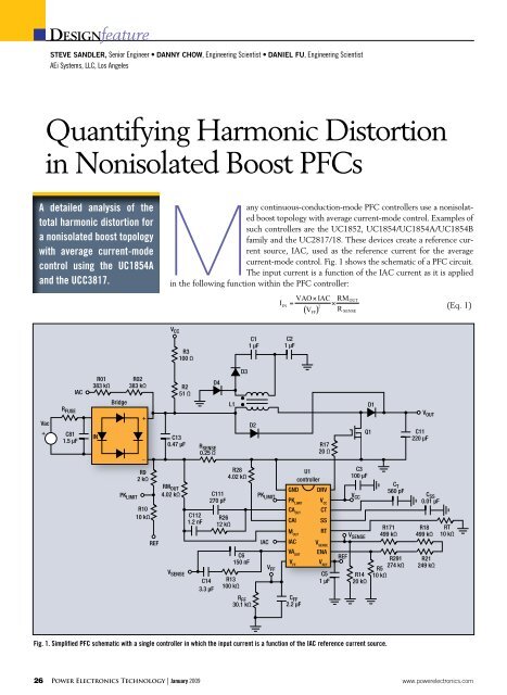
Many cont<strong>in</strong>uous-conduction-mode PFC controllers use a nonisolated<br />
boost topology with average current-mode control. Examples of<br />
such controllers are the UC1852, UC1854/UC1854A/UC1854B<br />
family and the UC2817/18. These devices create a reference cur-<br />
VFF<br />
rent source, IAC, used as the reference current for the average<br />
VFF current-mode control. Fig. 1 shows the schematic of a PFC circuit.<br />
The <strong>in</strong>put current is a function of the IAC current as it is applied<br />
<strong>in</strong> the follow<strong>in</strong>g function with<strong>in</strong> the PFC controller:<br />
V CC<br />
R3<br />
100 Ω<br />
R2<br />
51 Ω<br />
C13<br />
0.47 µF R SENSE<br />
0.25 Ω<br />
RM OUT<br />
4.02 kΩ<br />
V SENSE<br />
C112<br />
1.2 nF<br />
C14<br />
3.3 µF<br />
D4<br />
C111<br />
270 pF<br />
L1<br />
R26<br />
12 kΩ<br />
D3<br />
R28<br />
4.02 kΩ<br />
R13<br />
100 kΩ<br />
C6<br />
150 nF<br />
C1<br />
1 µF<br />
D2<br />
R FF<br />
30.1 kΩ<br />
26 <strong>Power</strong> <strong>Electronics</strong> Technology | January 2009 www.powerelectronics.com<br />
PK LIMIT<br />
IAC<br />
V FF<br />
C2<br />
1 µF<br />
U1<br />
controller<br />
GND DRV<br />
PKLIMIT CAOUT CAI<br />
MOUT IAC<br />
VAOUT VFF C FF<br />
2.2 µF<br />
FBR<br />
R17<br />
20 Ω<br />
V CC<br />
CT<br />
SS<br />
RT<br />
V SENSE<br />
ENA<br />
V REF<br />
C5<br />
1 µF<br />
C3<br />
100 µF<br />
Fig. 1. Simplified PFC schematic with a s<strong>in</strong>gle controller <strong>in</strong> which the <strong>in</strong>put current is a function of the IAC reference current source.<br />
REF<br />
V CC<br />
V SENSE<br />
D1<br />
Q1<br />
R14<br />
20 kΩ<br />
C T<br />
560 pF<br />
R171<br />
499 kΩ<br />
R5<br />
10 kΩ<br />
R291<br />
274 kΩ<br />
V OUT<br />
C11<br />
220 µF<br />
C SS<br />
0.01 µF<br />
R18<br />
499 kΩ<br />
R21<br />
249 kΩ<br />
(Eq. 1)<br />
RT<br />
10 kΩ<br />
VFF VFBR
ledflash<br />
Where:<br />
VAO = Output of the voltage-sens<strong>in</strong>g<br />
amplifier<br />
V FF = Scaled and filtered version of the<br />
<strong>in</strong>put voltage<br />
IAC = Current reference.<br />
Ideally, IAC is a scaled replica of the<br />
rectified <strong>in</strong>put voltage. This ultimately is<br />
the waveform that the current signal will<br />
follow.<br />
RM OUT = Term<strong>in</strong>at<strong>in</strong>g resistance for the<br />
multiplier output current.<br />
R SENSE = Input-current sens<strong>in</strong>g resistor.<br />
V FBR = Forward voltage of the <strong>in</strong>put<br />
rectifier diodes.<br />
V RMS = The AC <strong>in</strong>put voltage.<br />
V FF is used to stabilize the voltage-loop<br />
ga<strong>in</strong> aga<strong>in</strong>st <strong>in</strong>put-voltage variations.<br />
Conduction of IAC beg<strong>in</strong>s when the AC <strong>in</strong>put voltage<br />
exceeds the sum of two bridge-rectifier diodes and the voltage<br />
at the IAC p<strong>in</strong>, VIAC . The IAC p<strong>in</strong> is different for each<br />
controller, rang<strong>in</strong>g from as low as 0.5 V for the UC1854A/B, VFF VFF<br />
to a high of 6 V for the orig<strong>in</strong>al UC1854. This conduc- VFF<br />
VV FF FF<br />
tion angle can be determ<strong>in</strong>ed based on the <strong>in</strong>put voltage as VFF assumptions:<br />
VFBR = 0.75 V<br />
VFF<br />
VRMS = 85 V V<br />
RMS<br />
FF<br />
RIAC = 736 kΩ<br />
PRMS = 250 W<br />
VIAC = 1.4 V.<br />
Solv<strong>in</strong>g for θ<br />
FBR FBR<br />
FBR<br />
(Eq.2)<br />
(Eq.3)<br />
Thus, this is the angle at which current just beg<strong>in</strong>s flow<strong>in</strong>g<br />
through R AC. The <strong>in</strong>stantaneous current is then def<strong>in</strong>ed by:<br />
for angles from θ to π-θ and from θ+ to 2π-θ.<br />
(Eq.4)<br />
Due to the symmetrical nature of the waveform <strong>in</strong> both<br />
x and y directions, the Fourier coefficients can be evaluated<br />
with<strong>in</strong> a s<strong>in</strong>gle quadrant, us<strong>in</strong>g only A coefficients.<br />
FBR<br />
(Eq.5)<br />
Then, the peak magnitude of any harmonic from the fundamental<br />
to <strong>in</strong>f<strong>in</strong>ity can be determ<strong>in</strong>ed.<br />
RT1<br />
1 m (measurement?)<br />
V3<br />
Tran generators = SIN<br />
120 VPK<br />
A(1) = 1.5831 × 10⁻⁴<br />
A(2) = 0<br />
A(3) = 1.67082 × 10⁻⁶<br />
The Total <strong>Harmonic</strong> <strong>Distortion</strong> (THD) for any number of<br />
harmonics also can be determ<strong>in</strong>ed. For example, evaluat<strong>in</strong>g<br />
the THD up to the 13th Figure 2 AEi Systems<br />
harmonic:<br />
VV FF FF<br />
VF V<br />
VF BR<br />
FF<br />
BR<br />
VFBR Dist IAC = 1.406%.<br />
(Eq.6)<br />
www.powerelectronics.com January 2009 | <strong>Power</strong> <strong>Electronics</strong> Technology 27<br />
+<br />
R1<br />
100 MΩ<br />
L<strong>in</strong><br />
IN<br />
V6<br />
+<br />
B1<br />
Voltage<br />
V(3,4) > 0?<br />
I(R3):<br />
-I(R3)<br />
X2<br />
KBPC806<br />
+<br />
_<br />
FBR<br />
R2<br />
14.5 Ω<br />
Fig. 2. Schematic for the <strong>in</strong>put full-bridge diodes that contribute a THD of 1.54161%.<br />
R3<br />
1 MΩ<br />
VFF<br />
V FF<br />
D1<br />
unknown<br />
THD Due To THe Full-BrIDge DIoDeS<br />
Under this particular V operat<strong>in</strong>g condition, the THD is<br />
FF<br />
1.4%, based solely VFBRon the forward voltage of the <strong>in</strong>put rectifier<br />
diodes and the voltage at the VIAC p<strong>in</strong>. Fig. 2 shows the<br />
schematic of the <strong>in</strong>put full-bridge diodes. Individual harmonics<br />
can be evaluated as well.<br />
In Table 1 (page 30), the SPICE Fourier analysis results<br />
show that the THD is 1.54%.<br />
These results show that the majority of the THD is from<br />
the 3rd through the 9th harmonic,<br />
which is generally difficult to filter,<br />
while the higher order harmonics<br />
are generally filterable. There are no<br />
n<br />
A(n)<br />
A(1)<br />
even harmonics.<br />
VAo, VFF , rMouT AnD rSenSe ConTrIBuTIon To THD<br />
In addition to the full-bridge<br />
diodes, the ripples at the VAO<br />
and VFF p<strong>in</strong>s of the IC chip also<br />
<strong>in</strong>troduce distortion <strong>in</strong>to the system. The ripple at VAO is a<br />
function of the error amplifier frequency compensation. The<br />
VFF or VRMS ripple is a function of the specific controller. For<br />
%<br />
3 1.05541<br />
5 0.63226<br />
7 0.45057<br />
9 0.34935<br />
11 0.28472<br />
13 0.23979
ledflash<br />
example, the UC2817 uses an <strong>in</strong>ternal circuit to create the<br />
V FF signal with the addition of only a resistor and a capacitor.<br />
The UC1854A requires many additional components. The<br />
ripples at VAO and V FF are assumed to be 30 mV and 20 mV,<br />
respectively, based on simulation results. For the purposes<br />
here, the THD is therefore:<br />
VAO = 2.1 V<br />
VAO RIPPLE = 0.03 V<br />
V FFRIPPLE = 0.02 V<br />
K1 = 0.018<br />
RM OUT = 4020 Ω<br />
R SENSE = 0.15 Ω<br />
The distoration, <strong>in</strong>clud<strong>in</strong>g the VAO and VF terms, is<br />
def<strong>in</strong>ed <strong>in</strong> Eq. 7 (<strong>in</strong> box).<br />
Dist IAC = 2.09258%.<br />
V LINE<br />
85 to<br />
265<br />
V RMS<br />
AC2<br />
AC1<br />
IAC<br />
F1<br />
R21<br />
383 kΩ<br />
C14<br />
1.5 µF<br />
400 V<br />
R12<br />
2 kΩ<br />
R11<br />
10 kΩ<br />
R13<br />
383 kΩ<br />
D3<br />
V REF<br />
6 A<br />
600 V<br />
V CC<br />
R9<br />
4.02 kΩ<br />
R8<br />
12 kΩ<br />
D6<br />
(optional)<br />
R16<br />
100 Ω<br />
C13<br />
0.47 µF<br />
600 V<br />
R14<br />
0.25 Ω 5 W<br />
C8<br />
270 pF<br />
R7<br />
100 kΩ<br />
R15<br />
51 kΩ<br />
R10<br />
4.02 kΩ<br />
D5<br />
(optional)<br />
C9<br />
1.2 nF<br />
C7<br />
150 nF<br />
C15<br />
3.3 µF<br />
C6<br />
2.2 µF<br />
Fig. 3. Schematic for a PFC circuit us<strong>in</strong>g the uCC3817 as a controller.<br />
R6<br />
30 kΩ<br />
IAC<br />
D7<br />
L1<br />
1 mH<br />
High voltage —<br />
see EVM warn<strong>in</strong>gs<br />
and restrictions<br />
1<br />
2<br />
3<br />
4<br />
5<br />
6<br />
7<br />
8<br />
C10<br />
1 µF<br />
Now, the THD due to the full bridge, VAO, V FF , R SENSE<br />
and RM OUT is 2.09%.<br />
MAxIMuM DuTy-CyCle lIMITATIon To THD<br />
The next source of distortion is a result of the maximum<br />
duty cycle of the boost converter. The cont<strong>in</strong>uous-conduction<br />
transfer function of the boost topology is:<br />
(Eq.8)<br />
In the boost converter PFC, the output voltage is a constant,<br />
while the <strong>in</strong>put voltage changes <strong>in</strong> accordance with the<br />
s<strong>in</strong>usoidal signal. The m<strong>in</strong>imum <strong>in</strong>put voltage for the controller<br />
to regulate occurs at maximum duty cycle. Assum<strong>in</strong>g 97%<br />
maximum duty cycle,<br />
28 <strong>Power</strong> <strong>Electronics</strong> Technology | January 2009 www.powerelectronics.com<br />
D8<br />
GND<br />
PK LIMIT<br />
CA OUT<br />
CAI<br />
M OUT<br />
IAC<br />
VA OUT<br />
V FF<br />
Fig. 3 AEi Systems<br />
C11<br />
1 µF<br />
D2<br />
8 A, 600 V<br />
UCC3817<br />
DRV OUT<br />
V CC<br />
OVP/EN 10<br />
High temperature —<br />
see EVM warn<strong>in</strong>gs<br />
and restrictions<br />
16<br />
15<br />
CT 14<br />
SS 13<br />
RT 12<br />
V SENSE<br />
V REF<br />
11<br />
9<br />
D4<br />
Q1<br />
V REF<br />
D1<br />
6 A, 600 V<br />
R17<br />
20 Ω<br />
R3<br />
20 kΩ<br />
V CC<br />
C5<br />
1 µF<br />
V O<br />
C12<br />
220 µF<br />
450 V<br />
C3<br />
1 µF CER<br />
C2<br />
100 µF AI EI<br />
C4 0.01 µF<br />
R1<br />
12 kΩ<br />
R2<br />
499 kΩ<br />
C1 560 pF<br />
R19<br />
499 kΩ<br />
R20<br />
274 kΩ<br />
R5<br />
10 kΩ<br />
VO +<br />
V OUT<br />
385 Vdc<br />
V O<br />
GND<br />
High voltage —<br />
see EVM warn<strong>in</strong>gs<br />
and restrictions<br />
R4<br />
249 kΩ
ledflash<br />
V OUT = 380 V<br />
D MAX = 0.97<br />
V IN = V OUT (1-D MAX ) (Eq. 9)<br />
V IN = 11.4 V.<br />
The m<strong>in</strong>imum <strong>in</strong>put voltage for operation is 11.4 V.<br />
Therefore, the conduction angle due to the maximum duty<br />
cycle is:<br />
See Eq. 11 <strong>in</strong> box.<br />
(Eq. 10)<br />
θ = 0.10752°<br />
Now, the total harmonic distortion due to full-bridge<br />
diodes, V FF /VAO ripples, RM OUT , R SENSE and maximum<br />
duty cycle can be reformulated as shown <strong>in</strong> Eq. 12 (<strong>in</strong> box).<br />
The f<strong>in</strong>al THD for the system is 2.85%.<br />
THD AnAlySIS For Sluu077C (uCC3817)<br />
Referr<strong>in</strong>g to Fig. 3, the VAO RIPPLE is a function of C7<br />
along with R2 and R19. The pole created by R7 and C7 is<br />
approximately 10 Hz, so that the VAO RIPPLE equals:<br />
R2 = 499 kΩ<br />
R19 = 499 kΩ<br />
C7 = 0.15 µF<br />
For the output capacitor current:<br />
(Eq. 13)<br />
I OUT = 250/380 A<br />
C OUT = 250 uF<br />
F = 60 Hz<br />
(Eq.7)<br />
(Eq.11)<br />
(Eq. 14)<br />
(Eq. 15)<br />
(Eq. 16)<br />
C(1) = 0<br />
A(2) = 0.65789<br />
A(1) = 0<br />
B(2) = 0<br />
B(1) = 0<br />
The ripple voltage at the output capacitor, or any<br />
harmonic, is shown <strong>in</strong> Eq. 17.<br />
(Eq. 17)<br />
The VAO ripple at twice the l<strong>in</strong>e frequency, n=2, is<br />
calculated to be:<br />
www.powerelectronics.com January 2009 | <strong>Power</strong> <strong>Electronics</strong> Technology 29<br />
(Eq.12)
ledflash<br />
V LINE<br />
V1<br />
LSOURCE 25 nH<br />
V OFF = 0<br />
V AMPL = 120<br />
FREQ = 60<br />
U5<br />
In+<br />
VCC R161<br />
100 Ω<br />
R151<br />
24 kΩ<br />
RSOURCE 0.1 mΩ<br />
C8<br />
1.5 µF<br />
R11<br />
10<br />
MΩ<br />
KBPC808<br />
In-<br />
Out+ Out-<br />
number oF harmoniCS; 14 thd:1.54161%<br />
HarMonic frequency MagnituDe PHase norMal<br />
MagnituDe<br />
R12<br />
V<br />
383 kΩ<br />
RECT<br />
R13<br />
383 kΩ<br />
R181<br />
24 kΩ<br />
R15<br />
30.1<br />
kΩ<br />
V FF<br />
C5<br />
1.2<br />
nF<br />
R9<br />
12<br />
kΩ<br />
R7<br />
2 kΩ<br />
C9<br />
2.2<br />
µF<br />
R CURRENT SENSOR<br />
0.25 Ω<br />
C14<br />
0.47 µF<br />
IAC<br />
R2<br />
4.02<br />
kΩ M OUT<br />
+ –<br />
+ –<br />
D1<br />
HFA08TB60<br />
–<br />
+<br />
C15<br />
270<br />
pF<br />
CAO<br />
Limiter<br />
Ref 9<br />
R18<br />
10<br />
kΩ<br />
VREF PKLIMIT U7<br />
UCC2817 DRV +<br />
OUT<br />
–<br />
+<br />
–<br />
L1<br />
1 mH U8<br />
VIN Duty<br />
VOUT GND D<br />
BOOST2<br />
VAOUT VSENSE SS<br />
C1 R3<br />
2.2 µF 100 kΩ<br />
C2<br />
150 nF<br />
VAOUT VSENSE SS<br />
C4<br />
10 nF<br />
R4<br />
499 kΩ VOUT R5<br />
499 kΩ<br />
R6<br />
20 kΩ<br />
GND<br />
CAI<br />
R8<br />
4.02 kΩ<br />
RT<br />
OVP/EN<br />
Fig. 4. Sluu077C PFC circuit used for THD simulation exhibits a THD of 2.53871%.<br />
V FF<br />
V CC<br />
CT<br />
R19<br />
10 kΩ<br />
EN<br />
COUT 220 µF<br />
R10<br />
0.2 Ω<br />
MaxiMuM Duty (%) tHD (%)<br />
Table 2. For 85 V rMS <strong>in</strong>put and 250-W output power,<br />
the relationship between maximum duty cycle and<br />
total harmonic distortion as derived from MathCAD<br />
calculations.<br />
(Eq. 19)<br />
Then, we can solve VAO as a function<br />
of operat<strong>in</strong>g po<strong>in</strong>t (<strong>in</strong>put voltage and<br />
output power):<br />
D MAX = 0.97<br />
P OUT = 250 W<br />
K = 115<br />
VAO = 2.2 V<br />
F = 60 Hz<br />
C OUT = 250×10 -6<br />
C7 = 0.15 µF<br />
R FF = 30 kΩ<br />
C FF = 2.2 µF<br />
V RMS = 85 V.<br />
93 6.799<br />
95 4.064<br />
97 2.492<br />
99 2.132<br />
The nom<strong>in</strong>al THD of the application<br />
circuit shown <strong>in</strong> Fig. 4 is calculated<br />
to be 2.49% us<strong>in</strong>g the equations<br />
derived <strong>in</strong> this article. The THD result<br />
form a SPICE simulation is 2.54%.<br />
These results are very close and the differences<br />
are primarily due to the nonl<strong>in</strong>earity<br />
of the <strong>in</strong>put rectifier diodes,<br />
which is not <strong>in</strong>cluded <strong>in</strong> the equations<br />
for simplification.<br />
Dist IAC = 2.49237%<br />
Fourier components of transient<br />
response IAC<br />
DC component = 1.119095E-03.<br />
Typically, the range of maximum<br />
duty cycle of the UCC3817 is from 93%<br />
to 99% accord<strong>in</strong>g to its data sheet (see<br />
Table 2).<br />
The maximum duty cycle is the<br />
major contributor to the THD. The<br />
maximum duty cycle alone can <strong>in</strong>crease<br />
the THD by more than 100% when<br />
D MAX changes from 97% to 93%.<br />
30 <strong>Power</strong> <strong>Electronics</strong> Technology | January 2009 www.powerelectronics.com<br />
VCC C10<br />
20 µF<br />
R14<br />
274 kΩ<br />
R22<br />
10 kΩ<br />
(Eq. 18)<br />
Table 1. THD is slightly higher than the MathCAD calculation due to the nonl<strong>in</strong>ear characteristics of the diodes model.<br />
R20<br />
10 kΩ<br />
C12<br />
1 µF<br />
R17<br />
249 kΩ<br />
norMal<br />
PHase<br />
0 0 2.90541e-009 0 0 0 0<br />
1 60 0.000115736 179.802 179.802 1 0<br />
2 120 5.80794e-009 93.6039 93.6039 5.01826e-005 -86.198<br />
3 180 1.3533e-006 -2.0727 -2.0727 0.0116929 -181.87<br />
4 240 5.80859e-009 97.207 97.207 5.01882e-005 -82.595<br />
5 300 7.99073e-007 -3.1959 -3.1959 0.00690427 -183<br />
6 360 5.80877e-009 100.81 100.81 5.01898e-005 -78.992<br />
7 420 5.63648e-007 -3.9129 -3.9129 0.00487011 -183.71<br />
8 480 5.80895e-009 104.413 104.413 5.01913e-005 -75.389<br />
9 540 4.33166e-007 -4.0928 -4.0928 0.00374271 -183.89<br />
10 600 5.80912e-009 108.016 108.016 5.01928e-005 -71.786<br />
11 660 3.49991e-007 -3.6379 -3.6379 0.00302404 -183.44<br />
12 720 5.80935e-009 111.619 111.619 5.01948e-005 -68.183<br />
13 780 2.92229e-007 -2.4967 -2.4967 0.00252496 -182.3<br />
V OUT<br />
R16<br />
0.652 Ω