Keith Billings April 2003.indd - Power Electronics
Keith Billings April 2003.indd - Power Electronics
Keith Billings April 2003.indd - Power Electronics

You also want an ePaper? Increase the reach of your titles
YUMPU automatically turns print PDFs into web optimized ePapers that Google loves.
MAGNETIC COMPONENTS SPECIAL REPORT<br />
Designing Flyback Transformer for Discontinuous Mode<br />
Let’s return to the question, “Why Have an Air Gap?” initially<br />
posed in the <strong>Power</strong> Design article in the December<br />
2002 issue of <strong>Power</strong> <strong>Electronics</strong> Technology. In that article,<br />
we found that although an air gap won’t prevent saturation<br />
in true transformer applications, it does reduce the<br />
slope of the B/H loop, reducing permeability and inductance,<br />
and increasing the magnetizing current in the primary. We<br />
found even a small air gap benefi ts discontinuous forward<br />
designs, as the residual fl ux value will be nearer zero, allowing<br />
a larger working fl ux density range.<br />
Now, let’s examine one more example of the function<br />
of an air gap in a ferrite core, while providing a better understanding<br />
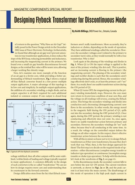
of fl yback transformers. Fig. 1 shows a typical<br />
off-line fl yback converter found in a low-power multiple<br />
output application. A major advantage of this topology is<br />
its low cost and simplicity. In multiple output applications,<br />
the addition of a secondary winding, a single diode, and an<br />
output capacitor is all that’s required for each additional<br />
isolated or common output. If one output is closed-loop<br />
<br />
<br />
<br />
<br />
<br />
<br />
<br />
<br />
<br />
Fig. 1. Typical off-line fl yback converter.<br />
voltage stabilized, then all other outputs will be semi-stabilized,<br />
(within limits of loading and voltage typically required<br />
in many applications). A common diffi culty in the design<br />
of such converters is the so-called “transformer.” We can see<br />
how its design requires more care and understanding than<br />
its counterpart in the forward converter.<br />
Design diffi culties stem from the fact that fl yback trans-<br />
<br />
<br />
<br />
<br />
<br />
<br />
<br />
<br />
<br />
<br />
<br />
<br />
<br />
By <strong>Keith</strong> <strong>Billings</strong>, DKB <strong>Power</strong> Inc., Ontario, Canada<br />
formers aren’t really transformers. More accurately, they’re<br />
inductors or chokes, depending on the mode of operation.<br />
They have additional windings called the secondaries. However,<br />
the secondary voltages aren’t related to the primary to<br />
secondary turn’s ratio, as they would normally be with a true<br />
transformer. Why is this?<br />
Look again at the phasing of the windings and diodes in<br />
Fig. 1. When Q1 is ON the input voltage is applied to the<br />
start of the primary winding (the dot end). This is positive,<br />
and an increasing current is fl owing in the primary (the<br />
magnetizing current). The phasing of the secondary windings<br />
and rectifi er diodes is such that the secondaries aren’t<br />
conducting during this period. Hence, the secondary windings<br />
effectively don’t exist, or at least the primary can’t “see”<br />
them. As a result, there’s no usable transformer action during<br />
the ON period of Q1.<br />
When Q1 turns OFF, the magnetizing current in the primary<br />
winding immediately stops. However, the core must<br />
now return to its previous condition of near-zero fl ux, and<br />
the voltage on all windings will reverse, creating the fl yback<br />
action. This brings the secondary windings and diodes into<br />
conduction and a decreasing (demagnetizing current) now<br />
fl ows in the secondaries. In other words, the energy stored<br />
in the magnetic fi eld during the ON period of Q1, spills<br />
out into the secondary during the OFF period of Q1. Once<br />
again, during this OFF period, the primary winding is not<br />
conducting and effectively does not exist. So, once again,<br />
there’s no usable transformer action between primary and<br />
secondary. However, the secondary windings do “see” each<br />
other, because they’re all conducting at the same time. As<br />
a result, the voltage on the controlled output defi nes the<br />
voltage on all other outputs. In this respect, there’s effective<br />
transformer action between the secondaries.<br />
With all this in mind, we know not to try to design fl yback<br />
transformers as if they were transformers, because they don’t<br />
work that way. What, then, is the best design approach for<br />
them? The fi rst step is to decide on the required mode of operation—either<br />
discontinuous (complete energy transfer or<br />
inductor type operation) or continuous (incomplete energy<br />
transfer or choke type operation). To help with this decision,<br />
let’s look at the waveforms of Fig. 2, on page 45.<br />
In the discontinuous mode, the secondary current falls to<br />
zero before the next Q1 ON period. The current waveform<br />
is sawtooth, as shown in Figs. 2a or<br />
2b, and the peak current<br />
is at least twice the mean current. The disadvantage of<br />
this mode of operation is the high peak ripple current in<br />
<strong>Power</strong> <strong>Electronics</strong> Technology <strong>April</strong> 2003 42<br />
www.powerelectronics.com
Fig. 2. (a)Discontinuous mode (boundry conditions); (b) Discontinuous<br />
mode (working condition with safety margin); ( c) Continuous mode<br />
(higher power condition).<br />
the transformer windings, diodes, transistors, and caps.<br />
Hence, this mode is more suitable for low power applications.<br />
Advantages are no dc component in the transformer;<br />
no reverse recovery problems in the output rectifi er diodes<br />
(they’re OFF before Q1 turns ON again) less turns; and no<br />
right-half-plane-zero in the transfer function [1] .<br />
In the continuous mode, the secondary current is greater<br />
than zero when Q1 turns ON for the next period. You can see<br />
<br />
<br />
<br />
<br />
POWER DESIGNS<br />
this in Fig. 2c. The main advantage is reduced ripple current.<br />
Unfortunately, the transformer must now support a dc current<br />
component. The output diodes are conducting when Q1<br />
turns ON (presenting diode reverse recovery problems), and<br />
it requires more turns while there’s a right-half-plane -zero<br />
in the transfer function. However, the advantage of much<br />
reduced ripple currents makes this mode more suitable for<br />
higher power applications.<br />
You can defi ne the mode of operation by adjusting the<br />
inductance. In this example, you can do this by adjusting the<br />
size of the air gap. Low inductance leads to the discontinuous<br />
mode, while large inductance leads to the continuous<br />
conduction mode. In general, the inductance may be adjusted<br />
by changing the turns, core material (permeability) or the<br />
size of the air gap, or a combination of these.<br />
Design Example—Discontinuous Mode<br />
At this stage, the design approach is best illustrated by considering<br />
a specifi c example. Assume a discontinuous mode<br />
of operation has been chosen (also known as the complete<br />
energy transfer mode) with 50 kHz operating frequency<br />
and a power of 100W. The ON period of Q1 is to be 40%<br />
of the total period or 8 µs and the OFF period will be 12 µs.<br />
This provides a 2 µs margin to ensure the mode remains<br />
discontinuous. As shown in Fig. 2b, other values can be used.<br />
CIRCLE 234 on Reader Service Card freeproductinfo.net/pet<br />
www.powerelectronics.com 45<br />
<strong>Power</strong> <strong>Electronics</strong> Technology <strong>April</strong> 2003
POWER DESIGNS<br />
This 40% conduction period occurs at<br />
the minimum input voltage of 100Vdc<br />
and full load. A gapped ferrite core is<br />
used, which has a center pole area of<br />
say 100 mm².<br />
At 100V input and 100W power, the<br />
time averaged primary input current<br />
will be 1A. The mean current in Q1 and<br />
the primary winding (P1), during the<br />
8 µs 40% ON period is 2.5A. The peak<br />
input current is twice the average or<br />
5A in this example (see this waveform<br />
in Fig. 2b).<br />
The required primary inductance<br />
can now be calculated using formula<br />
L(di/dt) = V, where di = 5A, dt = 8 µs<br />
and V = 100V. L will be 160 µH (see<br />
equations , on page 48).<br />
Now, Now t the<br />
minimum primary turns<br />
can be calculated. They are defi ned by<br />
the need to support the applied volt<br />
seconds ∆B—not by the inductance!<br />
The applied volt seconds equate to the<br />
parameter ∆B on the B/H loop shown<br />
in Fig. 3. This change in magnetic fl ux<br />
density ∆B will be maintained irre-<br />
spective of the size of the air gap—it<br />
generates within the primary winding<br />
the back mmf required to offset the<br />
applied volt seconds.<br />
We’ll choose a maximum core flux<br />
density of 0.2 Tesla to provide a good<br />
working margin on the saturation<br />
level of 0.35 Tesla. (Higher fl ux values<br />
will increase core loss but will result<br />
in less copper loss because less turns<br />
are required, and conversely). The<br />
optimum choice is where copper and<br />
core loss are equal. This is an iterative<br />
process, and cannot be fi nalized at this<br />
stage; it must be checked in the fi nal<br />
design. The following formula will<br />
yield the minimum primary turns for<br />
the chosen parameters:<br />
V t<br />
N min = × V t<br />
B × Ae A<br />
(See equations)<br />
Using the chosen values in the<br />
above formula, we fi nd the minimum<br />
primary turns are 40.<br />
Similarly, the secondary turns are<br />
defi ned by the need for the secondary<br />
CIRCLE 235 on Reader Service Card freeproductinfo.net/pet<br />
current to fall to zero before the next<br />
ON period of Q1. Once again, the turns<br />
are not calculated by transformer action,<br />
although they are a function of<br />
the required secondary voltage (see<br />
Figs. 2a and 2b). Fig. 2a shows the<br />
boundary condition where the secondary<br />
current just falls to zero just before<br />
the next ON period. Fig. 2b shows<br />
a better condition with more working<br />
margin where the current falls to<br />
zero in 10 µs, 2 µs before the next ON<br />
period. This allows for some load and<br />
tolerance variations but also increases<br />
the peak current slightly.<br />
Assume the secondary voltage is to<br />
be 20V. The fl yback period is 60% (12<br />
µs), and the time averaged secondary<br />
current for 100W output will be 5A.<br />
We have chosen to make secondary<br />
conduction period 10 µs. Hence, the<br />
mean current during the secondary<br />
conduction period of 10 µs is 10A,<br />
and the peak current is 20A. In this<br />
simplifi ed example, we’ve not made<br />
any allowance for diode drop and effi -<br />
ciency loss. Note the high output ripple<br />
current, peaking at 20A. Clearly, this<br />
isn’t a practical design and shows why<br />
the discontinuous mode is normally<br />
limited to low power applications.<br />
However, if the output voltage was to<br />
be larger—1000V, for example (you<br />
can do this with the flyback topology)—then<br />
the peak current would be<br />
only 400mA, which is fi ne.<br />
The secondary inductance required<br />
for 20V output and 10 µs conduction<br />
period may now be calculated in the<br />
same way as the primary inductance.<br />
Vs is now 20V and di/dt is 2A/µs.<br />
Evaluating, we get 10 µH (see appendix).<br />
Since the gap has already<br />
been defi ned by the primary design,<br />
we must now select the secondary<br />
turns to get this value of inductance<br />
in the secondary.<br />
The primary inductance (Lp) is<br />
160 µH for 40 turns, and inductance<br />
ratios as N² so 10 turns will give 10<br />
µH (see appendix). Less turns may be<br />
used, resulting in the current dropping<br />
to zero in a shorter fl yback period,<br />
moving more into the discontinuous<br />
mode, increasing the peak secondary<br />
current, and providing a wider zero<br />
<strong>Power</strong> <strong>Electronics</strong> Technology <strong>April</strong> 2003 46<br />
www.powerelectronics.com
Fig. 3. Top right quadrant of the B/H loop of the gapped core.<br />
<br />
<br />
<br />
<br />
<br />
POWER DESIGNS<br />
current margin. Conversely, more secondary turns may not<br />
allow the secondary current to reach zero during the fl yback<br />
period, and the continuous mode of operation will be entered.<br />
Neither the primary or secondary turns are defi ned<br />
by transformer action. However, if additional secondary<br />
windings are to be provided, their voltages will be defi ned by<br />
the transformer ratio between the various outputs, because<br />
they all conduct at the same time.<br />
To specify the output voltage, the control loop is closed<br />
to the chosen output and adjusts the duty ratio to maintain<br />
the output voltage at the chosen value for variations in input<br />
voltage and reduced loading. Increasing the loading beyond<br />
the designed 100W moves the action into the continuous<br />
mode. While this is possible, it complicates the design of<br />
both transformer and control loop because it introduces<br />
a RHP zero into the transfer function and introduces a dc<br />
component into the windings. If the control loop fails, the<br />
output voltage goes to a high and uncontrolled value, thus,<br />
overvoltage protection is a wise precaution.<br />
To optimize the design, calculate the core and copper<br />
loss at full load. They should be near equal for optimum<br />
design. If necessary, adjust the chosen fl ux value and turns<br />
to obtain this equality. Remember: Increasing the fl ux will<br />
increase core loss and decrease copper loss, since there will<br />
be less turns.<br />
CIRCLE 236 on Reader Service Card freeproductinfo.net/pet<br />
www.powerelectronics.com 47<br />
<strong>Power</strong> <strong>Electronics</strong> Technology <strong>April</strong> 2003
POWER DESIGNS<br />
We can now wind the transformer.<br />
The primary is wound using a wire<br />
gauge to fi ll less than 50% of the bobbin<br />
area to allow for insulation. The<br />
rest of the space is used for the secondaries.<br />
Several smaller diameter strands<br />
may be used in parallel to reduce skin<br />
effects.<br />
At the moment of turn OFF of Q1,<br />
the primary current (more correctly,<br />
ampere turns product) must commutate<br />
to the secondary. Any leakage<br />
inductance opposes this action, and a<br />
large voltage overshoot will be generated<br />
on the primary needing aggressive<br />
snubbing action. This problem is<br />
reduced by interleaving primary and<br />
secondary as you would in a forward<br />
transformer design.<br />
When fi nished, the core is fi tted using<br />
an elastic band to hold it together,<br />
and the core gap adjusted to obtain<br />
the required primary inductance of<br />
160 µH. For a better understanding,<br />
consider the action of the core gap in<br />
a somewhat different way. Energy is<br />
stored in the magnetic fi eld during the<br />
ON period of Q1 and transferred to the<br />
secondary during the OFF period of<br />
Q1. Fig. 3 shows the top right quadrant<br />
of the B/H loop of the gapped core,<br />
with the working value of fl ux density<br />
swing ∆B imposed on it. The area to<br />
the left of the B/H loop is proportional<br />
to the stored energy per cycle, while the<br />
much smaller area contained within<br />
the B/H loop is an indication of core<br />
loss (not to scale). In general,<br />
power = f × Ve ∫ H dB<br />
Equations<br />
Primary Inductance<br />
L<br />
P<br />
V P × ∆<br />
t<br />
=<br />
∆I<br />
Where:<br />
L P =Primary inductance (µH)<br />
V P = Primary voltage (V)<br />
∆t = Q1 ON time (µs)<br />
∆I = Peak primary current (A)<br />
Primary turns<br />
V P t<br />
NP<br />
=<br />
B Ae<br />
V t × V t<br />
B × A<br />
Where:<br />
t = Q1 ON time (µs)<br />
B = Peak fl ux density (tesla)<br />
Ae = effective area of center pole (mm2 )<br />
N = Minimum primary turns<br />
P<br />
Inductance factor<br />
LP<br />
AL<br />
= 2<br />
NP<br />
Where:<br />
A = Inductance of a single turn (µH)<br />
L<br />
2 Secondary inductance L = N × AL<br />
S S<br />
Where:<br />
L = Secondary inductance (µH)<br />
S<br />
N = Secondary turns<br />
S<br />
Secondary turns<br />
LS<br />
NS<br />
=<br />
AL<br />
Primary stored/transferred energy per<br />
2 cycle j = ½ L I (joules)<br />
P P<br />
Where:<br />
I = Peak primary current (A)<br />
P<br />
L = primary inductance (H)<br />
P<br />
CIRCLE 237 on Reader Service Card freeproductinfo.net/pet CIRCLE 238 on Reader Service Card freeproductinfo.net/pet<br />
<strong>Power</strong> <strong>Electronics</strong> Technology <strong>April</strong> 2003 48<br />
www.powerelectronics.com
2 Transferred power P = f × (½L I )= (W)<br />
P P<br />
Where:<br />
f = Frequency (Hz)<br />
2<br />
µ r × N P ×<br />
× Ae<br />
Air Gap =<br />
LP<br />
Where:<br />
Air gap = (mm)<br />
µr = 4 π × 10-7 N = Primary turns<br />
P<br />
Ae = Pole area (mm2 )<br />
L = Primary inductance (mH)<br />
P<br />
Increasing the Air Gap<br />
Increasing the air gap will swing the<br />
B/H loop more to the right, increasing<br />
the area and hence the stored energy.<br />
Most of the energy is stored in the air<br />
gap because this is the lowest permeability<br />
part of the magnetic path, getting<br />
something-for-nothing.<br />
The remnant fl ux (Br) also reduces<br />
as the core gap increases, slightly increasing<br />
the usable fl ux working range.<br />
The peak primary current increases as<br />
the inductance reduces. Since stored<br />
energy is proportional to Lp × Ip²,<br />
energy still increases with the larger<br />
gap—even though inductance falls.<br />
Below the B/H loop is shown the<br />
primary magnetizing current during<br />
the ON time of Q1. In pecked form, it<br />
shows the effective secondary demagnetizing<br />
current as would be refl ected<br />
to the primary winding in terms of<br />
ampere-turns. Of course, it does not<br />
actually fl ow in the primary. The ac<br />
fl ux swing ∆B remains constant irrespective<br />
of the core gap: It is a function<br />
of applied primary volt seconds. The<br />
peak current and stored energy are the<br />
dependant variables set by the size of<br />
the air gap. So now we see one more<br />
application for the air gap.<br />
For multiple outputs, simply sum<br />
the total output power and use this<br />
value in the equations when calculating<br />
the primary and secondary inductance<br />
of the main controlled output. The<br />
secondary currents will sort themselves<br />
out, depending on the loading applied<br />
POWER DESIGNS<br />
to each output.<br />
Even while ignoring the transformer<br />
action, (because it’s not a design<br />
parameter), it still exists. The fl yback<br />
voltage is refl ected back to the primary<br />
winding during the OFF period of<br />
Q1. Hence, reducing secondary turns<br />
increases secondary peak currents and<br />
increases the voltage stress on Q1 during<br />
the OFF period.<br />
Look for the follow-up article in the<br />
next issue of PETech. It will cover the<br />
transformer design for the continuous<br />
mode (or incomplete energy transfer<br />
choke mode). PETech<br />
<strong>Keith</strong> <strong>Billings</strong> is president of DKB <strong>Power</strong><br />
Inc., dkbp@rogers.com.<br />
Reference<br />
1. <strong>Keith</strong> <strong>Billings</strong>, “Switchmode <strong>Power</strong><br />
Supply Handbook,” McGraw-Hill ISBN<br />
0-07-006719-8.<br />
For more information on this article,<br />
CIRCLE 339 on Reader Service Card<br />
CIRCLE 239 on Reader Service Card freeproductinfo.net/pet<br />
www.powerelectronics.com 49<br />
<strong>Power</strong> <strong>Electronics</strong> Technology <strong>April</strong> 2003