- Page 1 and 2:
DESIGN OF A CUSTOM ASIC INCORPORATI
- Page 3 and 4:
ABSTRACT The vast majority of today
- Page 5 and 6:
LIST OF ABBREVIATIONS AND SYMBOLS A
- Page 7 and 8:
ISO International Organization for
- Page 9 and 10:
SI Serial In SO Serial Out SOF Star
- Page 11 and 12:
ACKNOWLEDGEMENTS I would like to ex
- Page 13 and 14:
2.4 Types of Devices...............
- Page 15 and 16:
4.3.5 Communication Speed Different
- Page 17 and 18:
5.3.21.1 Synchronization Test (test
- Page 19 and 20:
5.3 Resource Utilization...........
- Page 21 and 22:
LIST OF FIGURES 2.1 1 - Wire® Netw
- Page 23 and 24:
4.12 Read-Data Time Slot...........
- Page 25 and 26:
6.4 DS1996 Address Registers ......
- Page 27 and 28:
manufacturing process. Structured o
- Page 29 and 30:
describes the 1 - Wire® and CAN co
- Page 31 and 32:
2.2 1 - Wire® Overview The basis o
- Page 33 and 34:
All 1 - Wire® masters described in
- Page 35 and 36:
attachments, microcontroller with b
- Page 37 and 38:
Figure 2.3 Bidirectional port pin w
- Page 39 and 40:
2.3.3 Synthesizable 1 - Wire® Bus
- Page 41 and 42:
Figure 2.7 UART/RS232 Serial Port I
- Page 43 and 44:
hardware. Through control registers
- Page 45 and 46:
Table 2.2 1 - Wire® Bus Operations
- Page 47 and 48:
2.3.6 1 - Wire® Search Algorithm F
- Page 49 and 50:
detected. This ‘read two bits’
- Page 51 and 52:
in Figure 2.15. Alternatively, the
- Page 53 and 54:
of the bit, then write the desired
- Page 55 and 56:
2.4.2 Device Functions and Typical
- Page 57 and 58:
and development (R&D) investments b
- Page 59 and 60:
2.5 Network Types and Precedents As
- Page 61 and 62:
2.5.2 1 - Wire® Network Topologies
- Page 63 and 64:
2.5.3 1 - Wire® Network Limitation
- Page 65 and 66:
with a single selected slave. If an
- Page 67 and 68:
user group was founded in March of
- Page 69 and 70:
protocol on multiple media for maxi
- Page 71 and 72:
ecessive bit and the monitored stat
- Page 73 and 74:
specification: Start-Of-Frame, Arbi
- Page 75 and 76:
Cyclic Redundancy Check (CRC) Field
- Page 77 and 78:
Arbitration FieldThe Arbitration Fi
- Page 79 and 80:
SOF SOF Bit 28 Bit 27 Arbitration f
- Page 81 and 82:
Afterwards it starts transmitting s
- Page 83 and 84:
Figure 3.9 Structure of the Interfr
- Page 85 and 86:
error occurs, an Error Frame is gen
- Page 87 and 88:
Table 3.4 Error Flag Output Timing
- Page 89 and 90:
3.5.2 Error-Passive A node becomes
- Page 91 and 92:
where tNBT is the Nominal Bit Time
- Page 93 and 94:
Figure 3.12 Propagation Delay Betwe
- Page 95 and 96:
3.6.4 Synchronization t t t t (3.
- Page 97 and 98:
opposite value is inserted into the
- Page 99 and 100:
many systems, the bus length will b
- Page 101 and 102:
CHAPTER 4 THE CHALLENGES OF INTERFA
- Page 103 and 104:
In June 2004, Maxim Integrated Prod
- Page 105 and 106:
Wearable sensor technology is a new
- Page 107 and 108:
In traditional bus architectures, o
- Page 109 and 110:
Figure 4.3 Centralized arbiter with
- Page 111 and 112:
For the initial prototype design pr
- Page 113 and 114:
the ID of 31 transmits a ‘0’ (d
- Page 115 and 116:
Recently, a technique has been prop
- Page 117 and 118:
procedure, then the address claim p
- Page 119 and 120:
paradigms are prevalent in the desi
- Page 121 and 122:
systems possess a higher flexibilit
- Page 123 and 124:
fixed identifier and hence a fixed
- Page 125 and 126:
348sm Cm 47 8 smbit 11-bit hea
- Page 127 and 128:
est-case latency occurs when the bu
- Page 129 and 130:
to break the 1 - Wire® network int
- Page 131 and 132:
ow, is most critical for power deli
- Page 133 and 134:
computations have device-specific p
- Page 135 and 136:
Table 4.7 Example results with N 2
- Page 137 and 138:
4.3.5 Communication Speed Different
- Page 139 and 140:
anging” a port pin on a microproc
- Page 141 and 142:
From Figure 5.1, the block I/O pins
- Page 143 and 144:
5.2.2 Command Register In addition
- Page 145 and 146:
specifies the selected bit value to
- Page 147 and 148:
with i > m. This process is repeate
- Page 149 and 150:
Figure 5.6 Interrupt Register. OW_
- Page 151 and 152:
the INTR pin will be pulled high si
- Page 153 and 154:
master reset occurs. Table 5.2 show
- Page 155 and 156:
EN_FOW: Enable Force One Wire. Sett
- Page 157 and 158:
READ_ROM - Used to read the 64-bit
- Page 159 and 160:
5.2.8.1 Single Search ROM (single_s
- Page 161 and 162:
5.2.8.3 Scratchpad Memory (scratchp
- Page 163 and 164:
5.2.8.4 Command Recognition (cmd_re
- Page 165 and 166:
TBF - The Transmit Buffer provides
- Page 167 and 168:
compensate for the propagation dela
- Page 169 and 170:
Figure 5.15 CAN Module memory map [
- Page 171 and 172: ‘0’, fast speed mode will be us
- Page 173 and 174: COMP-SEL: Comparator Select. When t
- Page 175 and 176: Figure 5.18 CAN Status Register. B
- Page 177 and 178: that buffer is given to the CPU and
- Page 179 and 180: Acceptance Mask Registers (accepted
- Page 181 and 182: SJW1, SJW0: Synchronization Jump Wi
- Page 183 and 184: TSEG22 - TSEG10: Time Segment Bits.
- Page 185 and 186: The transmit clock (ttxclk) is used
- Page 187 and 188: 5.3.13 CAN Module Transmit Buffer I
- Page 189 and 190: Figure 5.28 CAN Transmit Data Segme
- Page 191 and 192: 5.3.20 CAN Node Overview As stated
- Page 193 and 194: Read Digital InputsRead the value o
- Page 195 and 196: the clock high time is either 5 µs
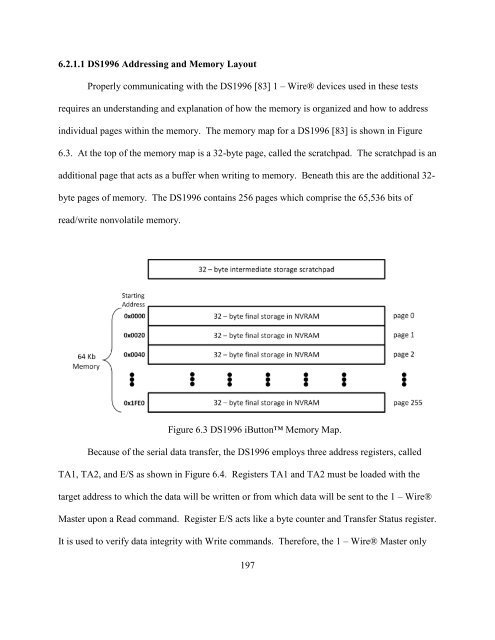
- Page 197 and 198: Yes Perform A/D Conversion on AN0 W
- Page 199 and 200: and GP2 and GP5 as outputs. With th
- Page 201 and 202: external INT pin, and then branches
- Page 203 and 204: Read MCP2515 Rx Buffer for Digital
- Page 205 and 206: When a valid message is received, t
- Page 207 and 208: Table 5.19 Resource Utilization. Re
- Page 209 and 210: For this test, only one CAN node wa
- Page 211 and 212: an Error Frame to be generated. Aft
- Page 213 and 214: messages, acknowledge messages, or
- Page 215 and 216: 5.3.21.4 Send Basic Frame Test (sen
- Page 217 and 218: going from one node to 30 nodes (se
- Page 219 and 220: Table 6.1 Resource Utilization. Rev
- Page 221: 6.2.1 Test Verification and Overvie
- Page 225 and 226: system configuration used for this
- Page 227 and 228: or not depends on the number of rec
- Page 229 and 230: 6.4. There are two receiving CAN no
- Page 231 and 232: CHAPTER 7 CONCLUSIONS AND FUTURE WO
- Page 233 and 234: a communication bus reset will occu
- Page 235 and 236: For the synthesizable CAN Controlle
- Page 237 and 238: additional CAN nodes were added to
- Page 239 and 240: Fall-Through Stack A LOW level on t
- Page 241 and 242: In conclusion, the prototype system
- Page 243 and 244: REFERENCES [1] IBM ASIC Products Ap
- Page 245 and 246: [22] “CAN - a brief tutorial for
- Page 247 and 248: [44] Microchip MCP2515 - Stand-Alon
- Page 249 and 250: [67] K. Tindell and A. Burns, “Gu
- Page 251 and 252: [88] “Verilog - A Language Refere