Explanation of Format - Smithsonian - The Chip Collection
Explanation of Format - Smithsonian - The Chip Collection
Explanation of Format - Smithsonian - The Chip Collection

Create successful ePaper yourself
Turn your PDF publications into a flip-book with our unique Google optimized e-Paper software.
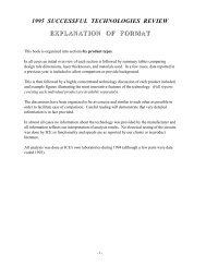
1996 SUCCESSFUL TECHNOLOGIES REVIEW<br />
EXPLANATION OF FORMAT<br />
This report is organized into sections by product types.<br />
In all cases an initial overview <strong>of</strong> each section is followed by summary tables comparing<br />
design rule dimensions, layer thicknesses, and materials used. In a few cases, data reported in<br />
a previous year is included to allow comparison or provide background.<br />
This is then followed by a highly concentrated technology discussion <strong>of</strong> each product included,<br />
and example figures illustrating the features <strong>of</strong> the technology. (Full reports covering each<br />
individual product are available separately).<br />
<strong>The</strong> discussions have been organized to be as concise and similar to each other as possible in<br />
order to facilitate ease <strong>of</strong> comparison. Careful reading will demonstrate that very detailed<br />
information is in fact provided.<br />
In almost all cases no information about the technology was provided by the manufacturer and<br />
all information reflects our interpretation <strong>of</strong> analysis results. No electrical testing <strong>of</strong> the circuits<br />
was done by ICE so functionality and speeds are as reported by our clients or in product<br />
literature.<br />
All analysis was done at ICE's own laboratories during 1995 or early 1996 (although a few<br />
parts were date coded 1994).<br />
- i -
OVERVIEW OF TECHNOLOGY STATUS<br />
JANUARY 1996<br />
It needs to be pointed out at the start that our comments below are based on technology we’ve<br />
actually seen appearing in real products, not the public announcements or discoveries that<br />
receive the bulk <strong>of</strong> the publicity in the press.<br />
<strong>The</strong> best illustration <strong>of</strong> this may again be in the area <strong>of</strong> DRAMs where it seems we’ve been<br />
deluged with announcements and advertisements for 64 Mbit devices for over three years —<br />
and in fact performed our first analysis on two types two years ago — but have seen nothing<br />
since until now. It was therefore very interesting to finally see the new Samsung 160 mm2 die<br />
version <strong>of</strong> this product, date coded week 52 <strong>of</strong> 1995, and compare it to the Hitachi part dated<br />
coded week 51 <strong>of</strong> 1993, almost exactly two years previous. Design rules were not improved<br />
although cell and die size were. We thus draw the conclusion that although manufacturers <strong>of</strong><br />
these product types have undoubtedly not been totally inactive, the priorities were obviously<br />
affected very significantly by the terrific markets for 16 Mbit parts and below.<br />
In fact, this lethargy in bringing larger capacity more advanced technology versions <strong>of</strong> memory<br />
devices into full production seems to have included the entire memory business.<br />
For example, the first 4 Mb SRAM we analyzed was done in 1992, on a part date coded week<br />
51 <strong>of</strong> 1991, over four years ago(!), and it had a die size smaller than the Toshiba part included<br />
here (date coded week 9 <strong>of</strong> 1995)!<br />
Somewhat similar comments can be made about EPROM.<br />
Obviously, there seems to have been much more emphasis on functional adaptations (wide<br />
organizations) than in technology advancements.<br />
This is entirely opposite to what has happened in the microprocessor arena where Intel alone<br />
has made more process technology advancements than the entire memory industry in the last<br />
year or two! In fact, from the first Pentium class device analyzed in 1993 (date code 9328) to<br />
- ii -
the 120 MHz/133 MHz devices analyzed in 1995 (presumably fabbed in mid-1995) these<br />
products have evolved from a really primitive example <strong>of</strong> process technology to a<br />
technological prowess that is the equivalent <strong>of</strong> the best we’ve seen. It clearly demonstrates that<br />
the wake-up call issued by IBM has been heard at Intel and may have resulted in waking up the<br />
giant, so to speak.<br />
Not that the other manufacturers in this business segment have been sitting idly by. IBM has<br />
made significant strides as well and Motorola is not far behind.<br />
In contrast, non-U.S. manufacturers <strong>of</strong>fering products in the microprocessor area have shown<br />
no evidence whatsoever in seriously addressing these changes in process technology, and we<br />
include the Hitachi SH2 as an example <strong>of</strong> this. NEC has been the most aggressive in the past,<br />
but we’ve seen no recent examples <strong>of</strong> their capability.<br />
- iii -
TABLE OF MOST<br />
AGGRESSIVE FEATURE SIZES<br />
<strong>The</strong> following table shows the most aggressive features ICE observed in 1995.<br />
FEATURE SIZES<br />
- iv -<br />
PRODUCT<br />
Largest die 190mm2 Hitachi SH2 Microprocessor<br />
Min metal 6 width 7.0μm IBM PC601+ Microprocessor<br />
Min metal 6 space 2.5μm IBM PC601+ Microprocessor<br />
Min metal 5 width 0.9μm IBM PC601+ Microprocessor<br />
Min metal 5 space 0.8μm IBM PC601+ Microprocessor<br />
Min metal 4 width 0.9μm IBM PC601+ Microprocessor<br />
Min metal 4 space 0.9μm IBM PC601+ Microprocessor<br />
Min metal 3 width 0.7μm Intel Pentium<br />
Min metal 3 space 0.5μm Intel Pentium<br />
Min metal 2 width 0.45μm IBM PC601+ Microprocessor<br />
Min metal 2 space 0.5μm Intel Pentium and NEC 1 Mb SRAM<br />
Min metal 1 width 0.3μm NEC 16 Mb DRAM<br />
Min metal 1 space 0.4μm Intel Pentium and Hitachi 1 Mb SRAM<br />
Min poly width (not as gate) 0.2μm Samsung 64 Mb DRAM<br />
Min via (metal to metal) 0.6μm Intel Pentium, Samsung and Galvantech<br />
1 Mb SRAMs<br />
Min contact (metal to silicon) 0.5μm Intel Pentium and Motorola PC603<br />
Min gate length N-channel/P-channel 0.25μm/0.25μm IBM PC601+ Microprocessor<br />
Min DRAM cell size 1.2μm 2 Samsung 64 Mb DRAM<br />
Min SRAM cell size 14.25μm2 Samsung 1 Mb SRAM<br />
Most levels <strong>of</strong> metal 6 IBM PC601+ Microprocessor<br />
Most levels <strong>of</strong> poly 5 Samsung 64 Mb DRAM<br />
Rated (ICE) most complex process Samsung 64 Mb DRAM<br />
Rated (ICE) most advanced technology IBM PC601+ Microprocessor
INDEX<br />
- v -<br />
Page<br />
<strong>Explanation</strong> <strong>of</strong> <strong>Format</strong> i<br />
Overview <strong>of</strong> Technology ii<br />
Table <strong>of</strong> Most Aggressive Feature Sizes iv<br />
Section 1 - DRAMs<br />
• Overview 1 - 1<br />
• Table 1-1 Horizontal Dimensions<br />
• Table 1-2 Vertical Dimensions<br />
• Table 1-3 Die Materials<br />
• Products<br />
- Samsung KM48V8100AS-6 64 Mbit DRAM 1 - 2<br />
- Fujitsu MB8116100-60PJ 16 Mbit DRAM 1 - 7<br />
- Mitsubishi M5M416400BTP-7 16 Mbit DRAM 1 - 11<br />
- NEC 4217400-60 16 Mbit DRAM 1 - 15<br />
Section 2 - SRAMs<br />
• Overview 2 - 1<br />
• Table 2-1 Horizontal Dimensions<br />
• Table 2-2 Vertical Dimensions<br />
• Table 2-3 Die Materials<br />
• Products<br />
- Toshiba TC554161FTL-70L 4 Mbit (256K x 16) SRAM 2 - 2<br />
- Samsung KM732V588 1 Mbit (32K x 32) SRAM 2 - 5<br />
- Galvantech GVT7132C32Q-7 1 Mbit (32K x 32) SRAM 2 - 9<br />
- Hitachi HM67W1664JP-12 1 Mbit (64K x 16) SRAM 2 - 12<br />
- NEC μPD461018LG5-A12 1 Mbit (64K x 18) SRAM 2 - 16<br />
- Motorola MCM67C618 1 Mbit (64K x 18) SRAM 2 - 20<br />
Section 3 - EPROM<br />
• Overview 3 - 1<br />
• Table 3-1 Horizontal Dimensions<br />
• Table 3-2 Vertical Dimensions<br />
• Table 3-3 Die Materials<br />
• Products<br />
- Xicor X28C010J-20 1 Mbit EEPROM 3 - 2<br />
- Hitachi HN58C1001P-12 1 Mbit EEPROM 3 - 5<br />
- Atmel AT27C010-45 4 Mbit EPROM 3 - 8<br />
- ISSI IS27HC010-30 1 Mbit EPROM 3 - 11
INDEX (continued)<br />
Section 4 - Programable Devices<br />
• Overview 4 - 1<br />
• Table 4-1 Horizontal Dimensions<br />
• Table 4-2 Vertical Dimensions<br />
• Table 4-3 Die Materials<br />
• Products<br />
- Xilinx XC5210 FPGA 4 - 2<br />
- Altera EPF81500ARC240-4 PLA 4 - 5<br />
- Altera EPM7256EQC160-20 EPLD 4- 8<br />
- Actel A1460A FPGA 4 - 11<br />
- Hitachi HG62G027 ASIC 4 - 14<br />
Section 5 - Microprocessors<br />
• Overview 5 - 1<br />
• Table 5-1 Horizontal Dimensions<br />
• Table 5-2 Vertical Dimensions<br />
• Table 5-3 Die Materials<br />
• Products<br />
- Intel A80502-120/133 "PENTIUM" 64-bit CPU (CISC) 5 - 2<br />
- IBM Power PC 601+ 64-bit CPU (RISC) 5 - 6<br />
- Motorola Power PC603 64-bit CPU (RISC) 5 - 10<br />
- AMD Am486DX4-100 32-bit CPU (CISC) 5 - 13<br />
- Hitachi SH-2 32-bit CPU (RISC) 5 - 16<br />
- vi -