PROGRAMMABLE ASICs
PROGRAMMABLE ASICs
PROGRAMMABLE ASICs

You also want an ePaper? Increase the reach of your titles
YUMPU automatically turns print PDFs into web optimized ePapers that Google loves.
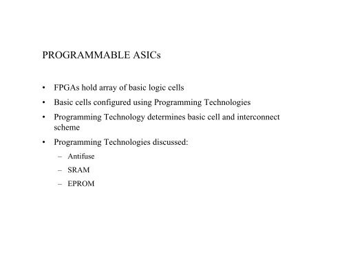
<strong>PROGRAMMABLE</strong> <strong>ASICs</strong><br />
• FPGAs hold array of basic logic cells<br />
• Basic cells configured using Programming Technologies<br />
• Programming Technology determines basic cell and interconnect<br />
scheme<br />
• Programming Technologies discussed:<br />
– Antifuse<br />
– SRAM<br />
– EPROM
Antifuse<br />
Actel antifuse<br />
• programming current (about 5 mA)<br />
• ( PLICE‘)<br />
• oxide–nitride–oxide ( ONO ) dielectric<br />
• Activator<br />
• in-system programming ( ISP )<br />
• gang programmers<br />
• one-time programmable (OTP) FPGAs
Metal–Metal Antifuse<br />
• QuickLogic metal–metal antifuse ( ViaLink‘)<br />
• alloy of tungsten, titanium, and silicon<br />
• bulk resistance of about 500 m W cm
Resistance values for the QuickLogic metal–metal antifuse
Static RAM<br />
Xilinx SRAM (static RAM)<br />
configuration cell<br />
• use in reconfigurable hardware<br />
• use of programmable read-only<br />
memory or PROM to hold<br />
configuration
EPROM and EEPROM Technology<br />
An EPROM transistor<br />
(a) With a high (> 12 V) programming voltage, V PP , applied to the drain,<br />
electrons gain enough energy to “jump” onto the floating gate (gate1)<br />
(b) Electrons stuck on gate1 raise the threshold voltage so that the transistor is<br />
always off for normal operating voltages<br />
(c) UV light provides enough energy for the electrons stuck on gate1 to “jump”<br />
back to the bulk, allowing the transistor to operate normally
FPGAs in Use<br />
• inventory<br />
• risk inventory or safety supply<br />
• just-in-time ( JIT )<br />
• printed-circuit boards ( PCBs )<br />
• pin locking or I/O locking
<strong>PROGRAMMABLE</strong> ASIC LOGIC CELLS<br />
Basic logic cell can be based on<br />
• Multiplexer<br />
• Look-up table<br />
• Programmable array logic
ACT 1 Logic Module<br />
The Actel ACT architecture<br />
(a) Organization of the basic logic cells<br />
(b) The ACT 1 Logic Module (LM, the Actel basic logic cell). The ACT 1 family uses just one<br />
type of LM. ACT 2 and ACT 3 FPGA families both use two different types of LM<br />
(c) An example LM implementation using pass transistors (without any buffering)<br />
(d) An example logic macro. Connect logic signals to some or all of the LM inputs, the<br />
remaining inputs to VDD or GND
Shannon’s Expansion Theorem<br />
• We can use the Shannon expansion theorem to expand F = A · F (A =<br />
'1') + A' · F (A = '0')<br />
• Example: F = A' · B + A · B · C' + A' · B' · C = A · (B · C') + A' · (B + B' · C)<br />
• F (A = '1') = B · C' is the cofactor of F with respect to ( wrt ) A or F A<br />
• If we expand F wrt B, F = A' · B + A · B · C' + A' · B' · C = B · (A' + A · C') +<br />
B' · (A' · C)<br />
• Eventually we reach the unique canonical form , which uses only minterms<br />
• (A minterm is a product term that contains all the variables of F—such as A ·<br />
B' · C)
example: F = (A · B) + (B' · C) + D<br />
• Expand F wrt B: F = B · (A + D) + B' · (C + D) = B · F2 +<br />
B' · F1<br />
• F = 2:1 MUX, with B selecting between two inputs: F (A<br />
= '1') and F (A = '0')<br />
• F also describes the output of the ACT 1 LM<br />
• Now we need to split up F1 and F2<br />
• Expand F2 wrt A, and F1 wrt C: F2 = A + D = (A · 1) +<br />
(A' · D); F1 = C + D = (C · 1) + (C' · D)<br />
• A, B, C connect to the select lines and '1' and D are the<br />
inputs of the MUXes in the ACT 1 LM<br />
• Connections: A0 = D, A1 = '1', B0 = D, B1 = '1', SA = C,<br />
SB = A, S0 = '0', and S1 = B
Timing Model and Critical Path<br />
(a) The C-Module for<br />
combinational logic<br />
(b) The ACT 2 S-Module<br />
(c) The ACT 3 S-Module<br />
(d) The equivalent circuit (without<br />
buffering) of the SE<br />
(sequential element)<br />
(e) The SE configured as a<br />
positive-edge–triggered D flip-<br />
flop
Timing views from inside and outside the Actel ACT S-module<br />
(a) Timing parameters for a<br />
'Std' speed grade ACT 3<br />
(b) Flip-flop timing<br />
(c) An example of flip-flop<br />
timing based on ACT 3<br />
parameters
Actel Logic Module Analysis<br />
• Actel uses a fine-grain architecture which allows you to use almost all<br />
of the FPGA<br />
• Synthesis can map logic efficiently to a fine-grain architecture<br />
• Physical symmetry simplifies place-and-route (swapping equivalent<br />
pins on opposite sides of the LM to ease routing)<br />
• Matched to small antifuse programming technology<br />
• LMs balance efficiency of implementation and efficiency of utilization<br />
• A simple LM reduces performance, but allows fast and robust placeand-route
XC3000 CLB (configurable logic block )
• A 32-bit look-up table ( LUT )<br />
• CLB propagation delay is fixed (the LUT access time) and independent of the logic<br />
function<br />
• 7 inputs to the XC3000 CLB: 5 CLB inputs (A–E), and 2 flip-flop outputs (QX and<br />
QY)<br />
• 2 outputs from the LUT (F and G). Since a 32-bit LUT requires only five variables to<br />
form a unique address (32 = 2 5 ), there are several ways to use the LUT:<br />
• Use 5 of the 7 possible inputs (A–E, QX, QY) with the entire 32-bit LUT (the CLB<br />
outputs (F and G) are then identical)<br />
• Split the 32-bit LUT in half to implement 2 functions of 4 variables each; choose 4<br />
input variables from the 7 inputs (A–E, QX, QY). You have to choose 2 of the inputs<br />
from the 5 CLB inputs (A–E); then one function output connects to F and the other<br />
output connects to G.<br />
• You can split the 32-bit LUT in half, using one of the 7 input variables as a select<br />
input to a 2:1 MUX that switches between F and G (to implement some functions of<br />
6 and 7 variables).
XC4000 Logic Block<br />
The Xilinx XC4000 family CLB (configurable logic block). ( Source: Xilinx.)
XC5200 Logic Block<br />
The Xilinx XC5200 family Logic Cell (LC) and configurable logic block (CLB).<br />
( Source: Xilinx.)
Xilinx LCA timing model (XC5210-6)
Altera FLEX<br />
(a) Chip floorplan<br />
(b) Logic Array Block (LAB)<br />
(c) Details of the Logic Element (LE)
Altera MAX<br />
Features:<br />
(a)<br />
Organization of<br />
logic and<br />
interconnect<br />
(b) LAB (Logic<br />
Array Block)<br />
(c) Macrocell<br />
• Logic expanders and expander terms ( helper terms) increase term efficiency<br />
• Shared logic expander ( shared expander, intranet) and parallel expander<br />
(internet)<br />
• Deterministic architecture allows deterministic timing before logic assignment<br />
• Any use of two-pass logic breaks deterministic timing<br />
• Programmable inversion increases term efficiency
Timing Model - Altera MAX