FDG6331L Integrated Load Switch - Guy Carpenter
FDG6331L Integrated Load Switch - Guy Carpenter
FDG6331L Integrated Load Switch - Guy Carpenter

You also want an ePaper? Increase the reach of your titles
YUMPU automatically turns print PDFs into web optimized ePapers that Google loves.
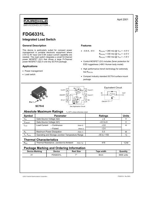
<strong>FDG6331L</strong><br />
<strong>Integrated</strong> <strong>Load</strong> <strong>Switch</strong><br />
General Description<br />
This device is particularly suited for compact power<br />
management in portable electronic equipment where<br />
2.5V to 8V input and 0.8A output current capability are<br />
needed. This load switch integrates a small N-Channel<br />
power MOSFET (Q1) that drives a large P-Channel<br />
power MOSFET (Q2) in one tiny SC70-6 package.<br />
Applications<br />
• Power management<br />
• <strong>Load</strong> switch<br />
Pin 1<br />
SC70-6<br />
Vin,R1<br />
ON/OFF<br />
R1,C1<br />
4<br />
5<br />
6<br />
Q2<br />
Features<br />
April 2001<br />
• –0.8 A, –8 V. RDS(ON) = 260 mΩ @ VGS = –4.5 V<br />
RDS(ON) = 330 mΩ @ VGS = –2.5 V<br />
RDS(ON) = 450 mΩ @ VGS = –1.8 V<br />
• Control MOSFET (Q1) includes Zener protection for<br />
ESD ruggedness (>6KV Human body model)<br />
• High performance trench technology for extremely<br />
low RDS(ON)<br />
• Compact industry standard SC70-6 surface mount<br />
package<br />
©2001 Fairchild Semiconductor Corporation <strong>FDG6331L</strong> Rev B(W)<br />
Q1<br />
See Application Circuit<br />
Absolute Maximum Ratings TA=25 o C unless otherwise noted<br />
3<br />
2<br />
1<br />
Vout,C1<br />
Vout,C1<br />
R2<br />
Equivalent Circuit<br />
IN + V – OUT<br />
DROP<br />
ON/OFF<br />
Symbol Parameter Ratings Units<br />
VIN Gate-Source Voltage (Q2) ± 8 V<br />
VON/OFF Gate-Source Voltage (Q1) –0.5 to 8 V<br />
I<strong>Load</strong> <strong>Load</strong> Current – Continuous (Note 2) –0.8 A<br />
– Pulsed (Note 2) –2.4<br />
PD Maximum Power Dissipation (Note 1) 0.3 W<br />
TJ, TSTG Operating and Storage Junction Temperature Range –55 to +150 °C<br />
Thermal Characteristics<br />
RθJA Thermal Resistance, Junction-to-Ambient (Note 1a) 415 °C/W<br />
Package Marking and Ordering Information<br />
Device Marking Device Reel Size Tape width Quantity<br />
.31 <strong>FDG6331L</strong> 7’’ 8mm 3000 units<br />
<strong>FDG6331L</strong>
Electrical Characteristics T A = 25°C unless otherwise noted<br />
Symbol Parameter Test Conditions Min Typ Max Units<br />
Off Characteristics<br />
BVIN Vin Breakdown Voltage VON/OFF = 0 V, ID = –250 µA 8 V<br />
I<strong>Load</strong> Zero Gate Voltage Drain Current VIN = –6.4 V, VON/OFF = 0 V –1 µA<br />
IFL Leakage Current, Forward VON/OFF = 0 V, VIN = 8 V 100 nA<br />
IRL Leakage Current, Reverse VON/OFF = 0 V, VIN = –8 V –100 nA<br />
On Characteristics (Note 2)<br />
VON/OFF (th) Gate Threshold Voltage VIN = VON/OFF, ID = –250 µA 0.4 0.9 1.5 V<br />
RDS(on)<br />
RDS(on)<br />
Static Drain–Source<br />
On–Resistance (Q2)<br />
Static Drain–Source<br />
On–Resistance (Q1)<br />
VIN = 4.5 V, ID = –0.8 A<br />
VIN =2.5 V, ID = –0.7 A<br />
VIN = 1.8 V, ID = –0.6 A<br />
VIN = 4.5 V, ID = 0.4A<br />
VIN = 2.7 V, ID = 0.2 A<br />
155<br />
193<br />
248<br />
310<br />
380<br />
260<br />
330<br />
450<br />
400<br />
500<br />
Drain–Source Diode Characteristics and Maximum Ratings<br />
IS Maximum Continuous Drain–Source Diode Forward Current –0.25 A<br />
VSD Drain–Source Diode Forward<br />
Voltage<br />
VON/OFF = 0 V, IS = –0.25 A(Note 2) –1.2 V<br />
Notes:<br />
1. RθJA is the sum of the junction-to-case and case-to-ambient thermal resistance where the case thermal reference is defined as the solder mounting surface of<br />
the drain pins. RθJC is guaranteed by design while RθJA is determined by the user’s board design.<br />
2. Pulse Test: Pulse Width < 300µs, Duty Cycle < 2.0%.<br />
<strong>FDG6331L</strong> <strong>Load</strong> <strong>Switch</strong> Application Circuit<br />
IN Q2<br />
OUT<br />
R1<br />
ON/OFF<br />
Q1<br />
R2<br />
C1<br />
LOAD<br />
External Component Recommendation:<br />
For additional in-rush current control, R2 and C1 can be added. For more information, see application note AN1030.<br />
mΩ<br />
mΩ<br />
<strong>FDG6331L</strong> Rev B (W)<br />
<strong>FDG6331L</strong>
Typical Characteristics<br />
-V DROP, (V)<br />
-V DROP, (V)<br />
1<br />
0.8<br />
0.6<br />
0.4<br />
0.2<br />
V IN = -1.8V<br />
V ON/OFF = -1.5-8V<br />
PW = 300us, D < 2%<br />
T J = 125 O C<br />
T J = 25 O C<br />
0<br />
0 0.4 0.8 1.2<br />
-IL, (A)<br />
1.6 2 2.4<br />
1<br />
0.8<br />
0.6<br />
0.4<br />
0.2<br />
Figure 1. Conduction Voltage Drop<br />
Variation with <strong>Load</strong> Current.<br />
V IN = -4.5V<br />
V ON/OFF = -1.5-8V<br />
PW = 300us, D < 2%<br />
T J = 125 O C<br />
T J = 25 O C<br />
0<br />
0 0.4 0.8 1.2<br />
-IL, (A)<br />
1.6 2 2.4<br />
Figure 3. Conduction Voltage Drop<br />
Variation with <strong>Load</strong> Current.<br />
R DS(ON), ON-RESISTANCE (Ω)<br />
-V DROP, (V)<br />
0.6<br />
0.5<br />
0.4<br />
0.3<br />
0.2<br />
0.1<br />
1<br />
0.8<br />
0.6<br />
0.4<br />
0.2<br />
V IN = -2.5V<br />
V ON/OFF = -1.5-8V<br />
PW = 300us, D < 2%<br />
T J = 125 O C<br />
T J = 25 O C<br />
0<br />
0 0.4 0.8 1.2<br />
-IL, (A)<br />
1.6 2 2.4<br />
Figure 2. Conduction Voltage Drop<br />
Variation with <strong>Load</strong> Current.<br />
T J = 25 O C<br />
T J = 125 O C<br />
I L = -1A<br />
V ON/OFF = 1.5 - 8V<br />
PW = 300us, D < 2%<br />
0<br />
1.25 2 2.75 3.5 4.25 5<br />
-VIN, INPUT VOLTAGE (V)<br />
Figure 4. On-Resistance Variation<br />
With Input Voltage<br />
<strong>FDG6331L</strong> Rev B (W)<br />
<strong>FDG6331L</strong>
TRADEMARKS<br />
The following are registered and unregistered trademarks Fairchild Semiconductor owns or is authorized to use and is<br />
not intended to be an exhaustive list of all such trademarks.<br />
ACEx<br />
Bottomless<br />
CoolFET<br />
CROSSVOLT<br />
DenseTrench<br />
DOME<br />
EcoSPARK<br />
E 2 CMOS TM<br />
EnSigna TM<br />
FACT<br />
FACT Quiet Series<br />
DISCLAIMER<br />
LIFE SUPPORT POLICY<br />
FAIRCHILD’S PRODUCTS ARE NOT AUTHORIZED FOR USE AS CRITICAL COMPONENTS IN LIFE SUPPORT<br />
DEVICES OR SYSTEMS WITHOUT THE EXPRESS WRITTEN APPROVAL OF FAIRCHILD SEMICONDUCTOR CORPORATION.<br />
As used herein:<br />
1. Life support devices or systems are devices or<br />
systems which, (a) are intended for surgical implant into<br />
the body, or (b) support or sustain life, or (c) whose<br />
failure to perform when properly used in accordance<br />
with instructions for use provided in the labeling, can be<br />
reasonably expected to result in significant injury to the<br />
user.<br />
PRODUCT STATUS DEFINITIONS<br />
Definition of Terms<br />
2. A critical component is any component of a life<br />
support device or system whose failure to perform can<br />
be reasonably expected to cause the failure of the life<br />
support device or system, or to affect its safety or<br />
effectiveness.<br />
Datasheet Identification Product Status Definition<br />
Advance Information<br />
Preliminary<br />
No Identification Needed<br />
Obsolete<br />
FAST ®<br />
FASTr<br />
GlobalOptoisolator<br />
GTO<br />
HiSeC<br />
ISOPLANAR<br />
LittleFET<br />
MicroFET<br />
MICROWIRE<br />
OPTOLOGIC<br />
OPTOPLANAR<br />
FAIRCHILD SEMICONDUCTOR RESERVES THE RIGHT TO MAKE CHANGES WITHOUT FURTHER<br />
NOTICE TO ANY PRODUCTS HEREIN TO IMPROVE RELIABILITY, FUNCTION OR DESIGN. FAIRCHILD<br />
DOES NOT ASSUME ANY LIABILITY ARISING OUT OF THE APPLICATION OR USE OF ANY PRODUCT<br />
OR CIRCUIT DESCRIBED HEREIN; NEITHER DOES IT CONVEY ANY LICENSE UNDER ITS PATENT<br />
RIGHTS, NOR THE RIGHTS OF OTHERS.<br />
Formative or<br />
In Design<br />
First Production<br />
Full Production<br />
Not In Production<br />
PACMAN<br />
POP<br />
PowerTrench ®<br />
QFET<br />
QS<br />
QT Optoelectronics<br />
Quiet Series<br />
SILENT SWITCHER<br />
SMART START<br />
Star* Power<br />
Stealth<br />
SuperSOT-3<br />
SuperSOT-6<br />
SuperSOT-8<br />
SyncFET<br />
TinyLogic<br />
UHC<br />
UltraFET®<br />
VCX<br />
This datasheet contains the design specifications for<br />
product development. Specifications may change in<br />
any manner without notice.<br />
This datasheet contains preliminary data, and<br />
supplementary data will be published at a later date.<br />
Fairchild Semiconductor reserves the right to make<br />
changes at any time without notice in order to improve<br />
design.<br />
This datasheet contains final specifications. Fairchild<br />
Semiconductor reserves the right to make changes at<br />
any time without notice in order to improve design.<br />
This datasheet contains specifications on a product<br />
that has been discontinued by Fairchild semiconductor.<br />
The datasheet is printed for reference information only.<br />
®<br />
Rev. H1