STEPPER MOTOR DRIVER VID66-06 - Guy Carpenter
STEPPER MOTOR DRIVER VID66-06 - Guy Carpenter
STEPPER MOTOR DRIVER VID66-06 - Guy Carpenter

You also want an ePaper? Increase the reach of your titles
YUMPU automatically turns print PDFs into web optimized ePapers that Google loves.
A Company of Wellgain Group<br />
Stepper Motor Driver<br />
(For four motors)<br />
© 2005 Data Instrumentation Technology<br />
E-mail: vid.info@wellgain.com Website:http://www.vid.wellgain.com/<br />
Type:<strong>VID66</strong><strong>06</strong><br />
Revision: 1<br />
Page:1/6<br />
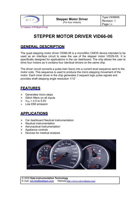
<strong>STEPPER</strong> <strong>MOTOR</strong> <strong>DRIVER</strong> <strong>VID66</strong>-<strong>06</strong><br />
GENERAL DESCRIPTION<br />
The quad stepping motor driver <strong>VID66</strong>-<strong>06</strong> is a monolithic CMOS device intended to be<br />
used as an interface circuit to ease the use of the stepper motor VID29-XX. It is<br />
specifically designed for applications in the car dashboard. The chip allows the user to<br />
drive four motors as it contains four identical drivers on the same chip.<br />
The driver circuit converts a pulse train f(scx) into a current level sequence sent to the<br />
motor coils. This sequence is used to produce the micro stepping movement of the<br />
motor. Each inner driver in the chip generates 2 sequent logic pulse signals and<br />
provides shaft stepping angle resolution 1/12°.<br />
FEATURES<br />
Generates micro steps<br />
Glitch filters on all inputs<br />
VDD = 4.5 to 5.5V<br />
Low EMI emission<br />
APPLICATIONS<br />
Car dashboard Nautical instrumentation<br />
Nautical instrumentation<br />
Aeronautical instrumentation<br />
Appliance controls<br />
Devices for medical analysis
A Company of Wellgain Group<br />
Stepper Motor Driver<br />
(For four motors)<br />
TYPICAL OPERATING CONFIGURATION<br />
MCU<br />
RESET<br />
f(scx)A<br />
CW/CCWA<br />
f(scx)B<br />
CW/CCWB<br />
f(scx)C<br />
CW/CCWC<br />
f(scx)D<br />
CW/CCWD<br />
PIN CONFIGURATION<br />
<strong>VID66</strong><strong>06</strong><br />
OUT<br />
A<br />
OUT<br />
B<br />
OUT<br />
C<br />
OUT<br />
© 2005 Data Instrumentation Technology<br />
E-mail: vid.info@wellgain.com Website:http://www.vid.wellgain.com/<br />
D<br />
Type:<strong>VID66</strong><strong>06</strong><br />
Revision: 1<br />
Page:2/6
A Company of Wellgain Group<br />
PIN DESCRIPTION<br />
Stepper Motor Driver<br />
(For four motors)<br />
© 2005 Data Instrumentation Technology<br />
E-mail: vid.info@wellgain.com Website:http://www.vid.wellgain.com/<br />
Type:<strong>VID66</strong><strong>06</strong><br />
Revision: 1<br />
Page:3/6<br />
Unused inputs must always be tied to a defined logic voltage level .<br />
Pin Number<br />
SOP - 28<br />
Name I/O Function<br />
1/15 VDD V Positive supply voltage<br />
12 VSS V Negative supply voltage<br />
28/3/14/17 f(scx) A/B/C/D I Stepping frequency; Driver A / B / C / D<br />
27/2/13/16 CW/CCW A/B/C/D I Direction of rotation; Driver A / B / C / D<br />
26 RESET I Reset for the four drivers<br />
4/5/6/7 OUT 3A/4A/2A/1A O Output driver A<br />
8/9/10/11 OUT 1D/2D/4D/3D O Output driver D<br />
18/19/20/21 OUT 3C/4C/2C/1C O Output driver C<br />
22/23/24/25 OUT 1B/2B/4B/3B O Output driver B<br />
OPERATING CONDITIONS<br />
Parameter Symbol<br />
Test<br />
Conditions<br />
Min Typ Max Units<br />
Operating temperature TA -40 +105 ℃<br />
Thermal impedance Rti SOP 80 ℃/W<br />
Supply voltage VDD 4.5 5 5.5 V<br />
Input voltage at any pin VIN VSS VDD V<br />
ELECTRICAL CHARACTERISTICS<br />
VDD = 4.5~5.5V, TA = -40~105°C, unless otherwise specified<br />
Parameter Symbol Test Conditions Min Typ Max Units<br />
Typical supply<br />
current<br />
IC<br />
VDD=5V,ω=200°/S,<br />
TA=25℃,RB25=280Ω<br />
76 mA<br />
Worst case supply<br />
current<br />
ICMAX<br />
VDD=5.5V,RESET=VSS,<br />
TA=-40℃,RB-40=190Ω<br />
200 mA<br />
Quiescent supply<br />
current<br />
ICC<br />
All inputs at VDD or VSS,<br />
no load<br />
300 μA<br />
Low<br />
voltage<br />
level input VIL VDD=4.5~5.5V VSS 1.35 V<br />
High<br />
voltage<br />
level input VIH VDD=4.5~5.5V 3.15 VDD V<br />
Input leakage IIN VIN=VSS or VDD -10 10 μA
A Company of Wellgain Group<br />
LOAD CHARACTERISTICS<br />
Stepper Motor Driver<br />
(For four motors)<br />
© 2005 Data Instrumentation Technology<br />
E-mail: vid.info@wellgain.com Website:http://www.vid.wellgain.com/<br />
Type:<strong>VID66</strong><strong>06</strong><br />
Revision: 1<br />
Page:4/6<br />
Parameter Symbol Test Conditions Min Typ Max Units<br />
Coil resistance<br />
RB25<br />
RB-40<br />
RB105<br />
VID29-XX,TA=25℃<br />
VID29-XX,TA=-40℃<br />
VID29-XX,TA=105℃<br />
260<br />
190<br />
350<br />
280 300<br />
Phase inductance L25 VID29-XX,TA=25℃ 0.4 H<br />
TIMING CHARACTERISTICS<br />
VDD = 4.5~5.5V, TA = -40~105°C, trise and tfall ≤ 20ns, input signal swing VSS to VDD<br />
Parameter Symbol Test Conditions Min Typ Max Units<br />
Signal pulse width tw high or low 450 ns<br />
Input frequency f(scx)<br />
Driver input limit 1.1 MHz<br />
Motor speed limit<br />
(=600°/s)<br />
1.1<br />
7.2<br />
MHz<br />
KHz<br />
Setup time to<br />
f(scx)<br />
ts high or low 100 ns<br />
RESET release<br />
time to f(scx)<br />
DELAY TIMING WAVEFORMS<br />
ABSOLUTE MAXIMUM RATINGS<br />
trr 100 ns<br />
Parameter Symbol Conditions<br />
Voltage VDD to VSS VDD -0.3~+6V<br />
Voltage at any pin to VDD VMAX +0.3V<br />
Voltage at any pin to VSS VMIN -0.3V<br />
Current at OUTs 1-4 IOUTMAX ±35mA<br />
Max. junction temperature Tj 150℃<br />
Operating temp. range TA -40~+105℃<br />
Storage temp. range TSTO -65~+125℃<br />
Ω<br />
Ω<br />
Ω
A Company of Wellgain Group<br />
HANDING PROCEDURES<br />
Stepper Motor Driver<br />
(For four motors)<br />
© 2005 Data Instrumentation Technology<br />
E-mail: vid.info@wellgain.com Website:http://www.vid.wellgain.com/<br />
Type:<strong>VID66</strong><strong>06</strong><br />
Revision: 1<br />
Page:5/6<br />
Stresses beyond these listed maximum ratings may cause permanent damage to the<br />
device. Exposure to conditions beyond specified operating conditions may affect<br />
device reliability or cause malfunction.<br />
The device has built-in protection against high static voltages or electric fields; however,<br />
anti-static precautions must be taken as for any other CMOS component. Unless<br />
otherwise specified, proper operation can only occur when all terminal voltages are<br />
kept within the supply voltage range. Unused inputs must always be tied to a defined<br />
logic voltage level unless otherwise specified.<br />
CIRCUIT PROTECTIONS<br />
To filter fast voltage transients, it is highly recommended to connect two 100nF ceramic<br />
capacitors to the power supply pins, one on either side and as close as possible to the<br />
chip.<br />
Moreover, to protect the chip against latch-up, a 5uF capacitor per motor connected<br />
should be added. Thus, for 4 motors, typically a 22uF capacitor must be used, either<br />
electrolytic or tantalum. Note this capacitor can be placed close to the voltage<br />
regulator.<br />
RECOMMENDED POWER UP<br />
In order to power up the circuit in a defined manner, it is recommended to keep the<br />
RESET input low while the VDD voltage is raising. After a delay of about 1ms, the<br />
RESET can be released (i.e. set high). Depending on the micro controller used, an<br />
external pull-down resistor might be required to properly set the RESET state at low<br />
during the start-up.<br />
FUNCTIONAL DESCRIPTION<br />
The rising edge of the f(scx) input signal moves the rotor by one micro step.<br />
The input signal "CW/CCW" (clockwise / counterclockwise) controls the direction of<br />
rotation of the motor.
A Company of Wellgain Group<br />
Stepper Motor Driver<br />
(For four motors)<br />
INPUT GLITCH FILTER & LEVEL SHIFTER<br />
© 2005 Data Instrumentation Technology<br />
E-mail: vid.info@wellgain.com Website:http://www.vid.wellgain.com/<br />
Type:<strong>VID66</strong><strong>06</strong><br />
Revision: 1<br />
Page:6/6<br />
All logic inputs of this driver are armed with a glitch filter to avoid erroneous information<br />
due to spikes and glitches on the input signal lines. All negative or positive pulses of<br />
less than 20 ns width are ignored.<br />
A minimum signal pulse width (positive or negative) of 450 ns guarantees correct<br />
function over the full temperature range.<br />
All logic inputs also feature a level shifter, which allows for operation of the circuit at a<br />
higher supply voltage (VDD) than the circuits driving the inputs. This is in order to drive<br />
the VID motors at a higher torque level.<br />
PACKAGE DIMENSIONS