Optoelectronics with Carbon Nanotubes
Optoelectronics with Carbon Nanotubes Optoelectronics with Carbon Nanotubes
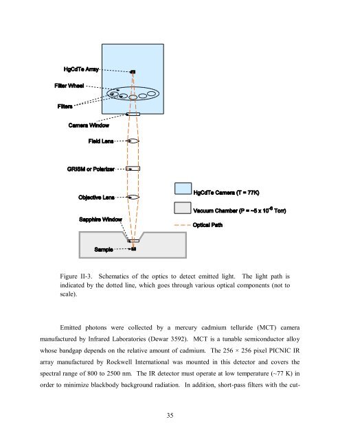
Figure II-3. Schematics of the optics to detect emitted light. The light path is indicated by the dotted line, which goes through various optical components (not to scale). Emitted photons were collected by a mercury cadmium telluride (MCT) camera manufactured by Infrared Laboratories (Dewar 3592). MCT is a tunable semiconductor alloy whose bandgap depends on the relative amount of cadmium. The 256 × 256 pixel PICNIC IR array manufactured by Rockwell International was mounted in this detector and covers the spectral range of 800 to 2500 nm. The IR detector must operate at low temperature (~77 K) in order to minimize blackbody background radiation. In addition, short-pass filters with the cut- 35
off wavelengths of 2150 nm, 2000 nm and 1800 nm were used to further improve the signal-to- noise ratio. It was found that most pixels on the array saturate after two seconds of integration with the 2150 nm filter. Hence, most measurements were taken with one-second integration time per frame. The optical system was calibrated for the spectral-dependent transmission or efficiency of all optical components using a black-body source with a known temperature. Spectra were measured by dispersing a point-source emission spatially with the GRISM, which was calibrated by krypton and xenon light sources chosen for their strong spectral lines within the detection window. The resulting wavelength resolution was better than 7 nm, with a systematic measurement error no larger than 7 nm. 4. Electroluminescence measurements The electrical transport and light emission properties were all measured in vacuum (~5 ×10 -6 Torr) to avoid oxidation and burning of the devices at high current. Light emission intensity as a function of applied voltage was measured by sweeping the applied voltage slowly while the IR detector recorded photon counts frame by frame. The total sweeping time was typically about two minutes. Current was measured simultaneously and was synchronized to the photon measurement. Photon signals were integrated spatially from multiple pixels to account for any de-focusing or movement of the stage during the measurement. Finally, the background was subtracted from each frame against neighboring pixels without signals, and also linearly against the beginning and end frames without any applied voltage to correct for any drifting in the response of the chip. For spectroscopy, it was often necessary to integrate the spatially (i.e. spectroscopically) dispersed signal across many frames in order to obtain a reasonable signal-to-noise ratio. The applied voltage was kept constant throughout the measurement period of tens to hundreds of seconds, while light image frames with one-second integration time were continuously taken. The current was also recorded throughout. Both the spectrum and the current were then averaged for analysis, and the background was subtracted from the spectral data in a similar manner as from the intensity data. 36
- Page 1 and 2: Stony Brook University The official
- Page 3 and 4: Stony Brook University The Graduate
- Page 5 and 6: diodes nonetheless show a rectifyin
- Page 7 and 8: Table of Contents Abstract ........
- Page 9 and 10: Chapter I List of Figures Figure
- Page 11 and 12: Figure V-3 Source-drain electric
- Page 13 and 14: My parents have been steadfast supp
- Page 15 and 16: This work explores both fundamental
- Page 17 and 18: In fact, we typically have no knowl
- Page 19 and 20: (a) (b) Figure I-2 (a) Energy dispe
- Page 21 and 22: (a) (b) metallic Figure I-4. One-di
- Page 23 and 24: optical absorption peaks for differ
- Page 25 and 26: elax rapidly to lower non-radiative
- Page 27 and 28: The disorder-induced band (D-band)
- Page 29 and 30: The saturation limit for semiconduc
- Page 31 and 32: (a) (b) Figure I-7. (a) A schematic
- Page 33 and 34: assisted tunneling through Schottky
- Page 35 and 36: majority carriers that gain enough
- Page 37 and 38: conventional ambipolar emission. Th
- Page 39 and 40: on quartz, which remains a signific
- Page 41 and 42: Chapter II Methods 1. Materials One
- Page 43 and 44: diameter (< 2 nm) SWNTs at IBM T. J
- Page 45 and 46: devices were annealed in vacuum at
- Page 47: 3. Experimental set-up The optical
- Page 51 and 52: Chapter III Unipolar, High-Bias Emi
- Page 53 and 54: Figure III-1. Semi-log plot of drai
- Page 55 and 56: wetting with CNTs 57 and a relative
- Page 57 and 58: Figure III-4. (Main panel) Electrol
- Page 59 and 60: By plotting the current as a functi
- Page 61 and 62: phonon temperature in broadening. S
- Page 63 and 64: found multiple tubes bound together
- Page 65 and 66: where i is the phonon mode, Tsub is
- Page 67 and 68: The main panel of Figure III-10 sho
- Page 69 and 70: the effect following Perebeinos’
- Page 71 and 72: the optical phonon population is no
- Page 73 and 74: (a) Figure III-13. (a) Spectra from
- Page 75 and 76: DOP = I║ / (I┴ + I║) = 0.77.
- Page 77 and 78: inding energy for perpendicular exc
- Page 79 and 80: 3. Conclusions We have examined the
- Page 81 and 82: In a split-gate scheme, a new level
- Page 83 and 84: 3. Electroluminescence mechanism an
- Page 85 and 86: After calibrating our detection sys
- Page 87 and 88: (a) (b) Figure IV-3. Electrolumines
- Page 89 and 90: observed by increasing the VGS valu
- Page 91 and 92: We claimed in Chapter III that in t
- Page 93 and 94: Let us finally comment on the effic
- Page 95 and 96: Chapter V The Polarized Carbon Nano
- Page 97 and 98: (a) (b) Figure V-1. (a) SEM image o
Figure II-3. Schematics of the optics to detect emitted light. The light path is<br />
indicated by the dotted line, which goes through various optical components (not to<br />
scale).<br />
Emitted photons were collected by a mercury cadmium telluride (MCT) camera<br />
manufactured by Infrared Laboratories (Dewar 3592). MCT is a tunable semiconductor alloy<br />
whose bandgap depends on the relative amount of cadmium. The 256 × 256 pixel PICNIC IR<br />
array manufactured by Rockwell International was mounted in this detector and covers the<br />
spectral range of 800 to 2500 nm. The IR detector must operate at low temperature (~77 K) in<br />
order to minimize blackbody background radiation. In addition, short-pass filters <strong>with</strong> the cut-<br />
35


