Optoelectronics with Carbon Nanotubes
Optoelectronics with Carbon Nanotubes Optoelectronics with Carbon Nanotubes
Furthermore, the fraction of spectral weight transfer is expected to depend on the nanotube diameter, which was also observed in a PLE experiment 29 . The appearance of such a phonon side band is another strong evidence for the dominance of excitonic transitions in SWNT light emission and absorption. In Perebeinos’ theoretical work, some of the spectral weight was also found to be transferred to the coupling to the RBM phonons, which is very close to the exciton line because of the low energy of the RBM phonons near the Γ point 39 . More recently, an updated theoretical work taking multiphonon sidebands into account also suggested the presence of a sideband due to RBM phonons, in addition to a prominent sideband due to the LO phonon coupling with the bright exciton 45 . The presence of an exciton-phonon sideband has also been observed in metallic SWNTs using Raleigh scattering spectroscopy 46 , highlighting the importance of excitons even in metallic tubes in which screening plays a greater role and exciton binding energy should be smaller. Given the prominent characteristics of phonon modes in SWNTs and their strong coupling to excitons, phonons are expected to play an important part in EL as well. 5. Transport mechanism in semiconducting SWNT devices In EL, carrier transport is an essential aspect of the operating principle because it is by electrically exciting carriers in a device that a CNT generates light. Here, we discuss electrical transfer characteristics of SWNTs, with the main focus on semiconducting tubes, since this work explores EL originating from excitation of carriers across the bandgap. Electrical emission from metallic tubes has also been observed and will be touched on briefly in the subsequent section on the history of EL theory and observations. One of the remarkable characteristics of carbon nanotubes is their extraordinary ability to withstand a current density exceeding 10 9 A/cm 2 47-49 . For metallic nanotubes, the current- carrying capability seems to hit a limit at 25 μA by Joule self-heating 50 and by the scattering of optical phonons 49, 51-53 . Since the inelastic optical phonon scattering length is about 10-15 nm 54 , a SWNT can carry even more current, up to 100 μA 55 if the channel is shorter than that characteristic length. 15
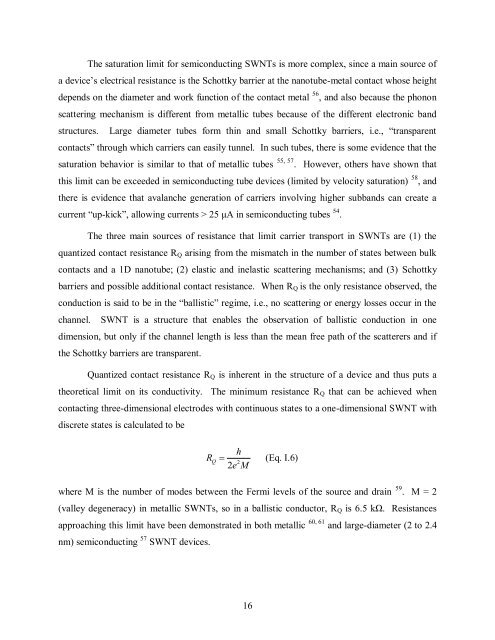
The saturation limit for semiconducting SWNTs is more complex, since a main source of a device’s electrical resistance is the Schottky barrier at the nanotube-metal contact whose height depends on the diameter and work function of the contact metal 56 , and also because the phonon scattering mechanism is different from metallic tubes because of the different electronic band structures. Large diameter tubes form thin and small Schottky barriers, i.e., “transparent contacts” through which carriers can easily tunnel. In such tubes, there is some evidence that the saturation behavior is similar to that of metallic tubes 55, 57 . However, others have shown that this limit can be exceeded in semiconducting tube devices (limited by velocity saturation) 58 , and there is evidence that avalanche generation of carriers involving higher subbands can create a current “up-kick”, allowing currents > 25 μA in semiconducting tubes 54 . The three main sources of resistance that limit carrier transport in SWNTs are (1) the quantized contact resistance RQ arising from the mismatch in the number of states between bulk contacts and a 1D nanotube; (2) elastic and inelastic scattering mechanisms; and (3) Schottky barriers and possible additional contact resistance. When RQ is the only resistance observed, the conduction is said to be in the “ballistic” regime, i.e., no scattering or energy losses occur in the channel. SWNT is a structure that enables the observation of ballistic conduction in one dimension, but only if the channel length is less than the mean free path of the scatterers and if the Schottky barriers are transparent. Quantized contact resistance RQ is inherent in the structure of a device and thus puts a theoretical limit on its conductivity. The minimum resistance RQ that can be achieved when contacting three-dimensional electrodes with continuous states to a one-dimensional SWNT with discrete states is calculated to be R Q h (Eq. I.6) 2 2eM where M is the number of modes between the Fermi levels of the source and drain 59 . M = 2 (valley degeneracy) in metallic SWNTs, so in a ballistic conductor, RQ is 6.5 kΩ. Resistances approaching this limit have been demonstrated in both metallic 60, 61 and large-diameter (2 to 2.4 nm) semiconducting 57 SWNT devices. 16
- Page 1 and 2: Stony Brook University The official
- Page 3 and 4: Stony Brook University The Graduate
- Page 5 and 6: diodes nonetheless show a rectifyin
- Page 7 and 8: Table of Contents Abstract ........
- Page 9 and 10: Chapter I List of Figures Figure
- Page 11 and 12: Figure V-3 Source-drain electric
- Page 13 and 14: My parents have been steadfast supp
- Page 15 and 16: This work explores both fundamental
- Page 17 and 18: In fact, we typically have no knowl
- Page 19 and 20: (a) (b) Figure I-2 (a) Energy dispe
- Page 21 and 22: (a) (b) metallic Figure I-4. One-di
- Page 23 and 24: optical absorption peaks for differ
- Page 25 and 26: elax rapidly to lower non-radiative
- Page 27: The disorder-induced band (D-band)
- Page 31 and 32: (a) (b) Figure I-7. (a) A schematic
- Page 33 and 34: assisted tunneling through Schottky
- Page 35 and 36: majority carriers that gain enough
- Page 37 and 38: conventional ambipolar emission. Th
- Page 39 and 40: on quartz, which remains a signific
- Page 41 and 42: Chapter II Methods 1. Materials One
- Page 43 and 44: diameter (< 2 nm) SWNTs at IBM T. J
- Page 45 and 46: devices were annealed in vacuum at
- Page 47 and 48: 3. Experimental set-up The optical
- Page 49 and 50: off wavelengths of 2150 nm, 2000 nm
- Page 51 and 52: Chapter III Unipolar, High-Bias Emi
- Page 53 and 54: Figure III-1. Semi-log plot of drai
- Page 55 and 56: wetting with CNTs 57 and a relative
- Page 57 and 58: Figure III-4. (Main panel) Electrol
- Page 59 and 60: By plotting the current as a functi
- Page 61 and 62: phonon temperature in broadening. S
- Page 63 and 64: found multiple tubes bound together
- Page 65 and 66: where i is the phonon mode, Tsub is
- Page 67 and 68: The main panel of Figure III-10 sho
- Page 69 and 70: the effect following Perebeinos’
- Page 71 and 72: the optical phonon population is no
- Page 73 and 74: (a) Figure III-13. (a) Spectra from
- Page 75 and 76: DOP = I║ / (I┴ + I║) = 0.77.
- Page 77 and 78: inding energy for perpendicular exc
The saturation limit for semiconducting SWNTs is more complex, since a main source of<br />
a device’s electrical resistance is the Schottky barrier at the nanotube-metal contact whose height<br />
depends on the diameter and work function of the contact metal 56 , and also because the phonon<br />
scattering mechanism is different from metallic tubes because of the different electronic band<br />
structures. Large diameter tubes form thin and small Schottky barriers, i.e., “transparent<br />
contacts” through which carriers can easily tunnel. In such tubes, there is some evidence that the<br />
saturation behavior is similar to that of metallic tubes 55, 57 . However, others have shown that<br />
this limit can be exceeded in semiconducting tube devices (limited by velocity saturation) 58 , and<br />
there is evidence that avalanche generation of carriers involving higher subbands can create a<br />
current “up-kick”, allowing currents > 25 μA in semiconducting tubes 54 .<br />
The three main sources of resistance that limit carrier transport in SWNTs are (1) the<br />
quantized contact resistance RQ arising from the mismatch in the number of states between bulk<br />
contacts and a 1D nanotube; (2) elastic and inelastic scattering mechanisms; and (3) Schottky<br />
barriers and possible additional contact resistance. When RQ is the only resistance observed, the<br />
conduction is said to be in the “ballistic” regime, i.e., no scattering or energy losses occur in the<br />
channel. SWNT is a structure that enables the observation of ballistic conduction in one<br />
dimension, but only if the channel length is less than the mean free path of the scatterers and if<br />
the Schottky barriers are transparent.<br />
Quantized contact resistance RQ is inherent in the structure of a device and thus puts a<br />
theoretical limit on its conductivity. The minimum resistance RQ that can be achieved when<br />
contacting three-dimensional electrodes <strong>with</strong> continuous states to a one-dimensional SWNT <strong>with</strong><br />
discrete states is calculated to be<br />
R<br />
Q<br />
h<br />
(Eq. I.6)<br />
2<br />
2eM<br />
where M is the number of modes between the Fermi levels of the source and drain 59 . M = 2<br />
(valley degeneracy) in metallic SWNTs, so in a ballistic conductor, RQ is 6.5 kΩ. Resistances<br />
approaching this limit have been demonstrated in both metallic 60, 61 and large-diameter (2 to 2.4<br />
nm) semiconducting 57 SWNT devices.<br />
16


