Optoelectronics with Carbon Nanotubes
Optoelectronics with Carbon Nanotubes Optoelectronics with Carbon Nanotubes
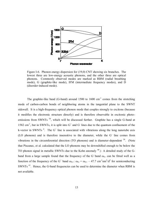
Figure I-6. Phonon energy dispersion for (19,0) CNT showing six branches. The lowest three are low-energy acoustic phonons, and the other three are optical phonons. Commonly observed modes are marked as RBM (radial breathing mode), G (graphite-like mode), IFM (intermediate frequency modes), and D (disorder-induced mode). The graphite-like band (G-band) around 1500 to 1600 cm -1 comes from the stretching mode of carbon-carbon bonds of neighboring atoms in the tangential plane to the SWNT sidewall. It is a high-frequency optical phonon mode that couples strongly to excitons (because it modifies the electronic structure directly) and is therefore observable in excitonic photo- emissions from SWNTs 39 , which will be discussed further. Graphite has a single G-band at 1582 cm -1 , but in SWNTs, it is split into G + and G - lines due to the quantum confinement of the k-vector in SWNTs 6 . The G + line is associated with vibrations along the long nanotube axis (LO phonons) and is therefore insensitive to the diameter, while the G - line comes from vibrations in the circumferential direction (TO phonons) and is diameter-dependent 38 . (Note that Piscanec, et al. calculated that the LO phonons may be downshifted enough to be below the TO phonon signal in metallic SWNTs due to the Kohn anomaly 40 .) A detailed study of the G- band from a large sample found that the frequency of the G - band ωG- can be fitted well as a function of the frequency of the G + band ωG+: ωG- = ωG+ – 47.7 cm -1 nm 2 /d 2 for semiconducting SWNTs 41 . Hence, the G-band frequencies can be used to determine the diameter when RBM is not available. 13
The disorder-induced band (D-band) is observed at 1300 to 1400 cm -1 and originates from symmetry breaking that occurs because of impurities, structural defects, etc., which couples the laser photons with the phonons near the K and K’ points of the Brillouin zone (Figure I-6). It is the most common second-order feature, which appears as a result of relaxing the selection-rule in sp 2 -hybridized carbon structures 38 . Because it is dependent on the presence of disorders, its relative intensity with respect to the G-band is used to gauge the structural integrity of a single tube or the purity of bulk nanotube samples. For example, this line could be virtually absent in chemical-vapor deposition (CVD) grown SWNTs that have not gone through additional chemical processing 42 . The CVD process is discussed in greater detail in the Methods section. There are other lines from second-order phonon processes that are commonly seen. One of them is the G’-band (or 2D-band) at 2600 cm -1 , which is the first overtone of the D-band. Another common second-order phonon signature is the IFMs (intermediate frequency modes) that show up as low-intensity features between RBM and the D-band. They can be explained as double-resonant processes involving two phonons that connect two electronic states 38 . While these and other second-order processes are commonly observed in RRS, it is the G-band that has been of utmost interest in spectral features of SWNT emission because of the strong coupling of the high-frequency optical phonons to excitons. 4. Exciton-phonon coupling in SWNTs Distinct satellite peaks to a main electronic-level transition (E11 and/or E22) have been observed in photoluminescence excitation (PLE) 29, 30, 43 , PL 44 , and photoconductivity (PC) spectra 27 , the strongest one being at approximately 200 meV from the main peak and showing a characteristic asymmetric shape. Perebeinos, et al. theoretically investigated the role of coupling between excitons and phonons in optical absorption by solving the Bethe-Salpeter equation with Hamiltonian that takes into account electron-phonon interactions 39 . They found that a significant fraction (8% for a (17, 0) tube) of the total spectral weight is transferred to exciton- phonon complexes, especially to the coupling of excitons and optical LO phonons at about 200 meV from the main peak, with an asymmetric lineshape. For free-carrier transitions, coupling to the phonons was found to merely modify the main peak somewhat, without creating a side band. 14
- Page 1 and 2: Stony Brook University The official
- Page 3 and 4: Stony Brook University The Graduate
- Page 5 and 6: diodes nonetheless show a rectifyin
- Page 7 and 8: Table of Contents Abstract ........
- Page 9 and 10: Chapter I List of Figures Figure
- Page 11 and 12: Figure V-3 Source-drain electric
- Page 13 and 14: My parents have been steadfast supp
- Page 15 and 16: This work explores both fundamental
- Page 17 and 18: In fact, we typically have no knowl
- Page 19 and 20: (a) (b) Figure I-2 (a) Energy dispe
- Page 21 and 22: (a) (b) metallic Figure I-4. One-di
- Page 23 and 24: optical absorption peaks for differ
- Page 25: elax rapidly to lower non-radiative
- Page 29 and 30: The saturation limit for semiconduc
- Page 31 and 32: (a) (b) Figure I-7. (a) A schematic
- Page 33 and 34: assisted tunneling through Schottky
- Page 35 and 36: majority carriers that gain enough
- Page 37 and 38: conventional ambipolar emission. Th
- Page 39 and 40: on quartz, which remains a signific
- Page 41 and 42: Chapter II Methods 1. Materials One
- Page 43 and 44: diameter (< 2 nm) SWNTs at IBM T. J
- Page 45 and 46: devices were annealed in vacuum at
- Page 47 and 48: 3. Experimental set-up The optical
- Page 49 and 50: off wavelengths of 2150 nm, 2000 nm
- Page 51 and 52: Chapter III Unipolar, High-Bias Emi
- Page 53 and 54: Figure III-1. Semi-log plot of drai
- Page 55 and 56: wetting with CNTs 57 and a relative
- Page 57 and 58: Figure III-4. (Main panel) Electrol
- Page 59 and 60: By plotting the current as a functi
- Page 61 and 62: phonon temperature in broadening. S
- Page 63 and 64: found multiple tubes bound together
- Page 65 and 66: where i is the phonon mode, Tsub is
- Page 67 and 68: The main panel of Figure III-10 sho
- Page 69 and 70: the effect following Perebeinos’
- Page 71 and 72: the optical phonon population is no
- Page 73 and 74: (a) Figure III-13. (a) Spectra from
- Page 75 and 76: DOP = I║ / (I┴ + I║) = 0.77.
Figure I-6. Phonon energy dispersion for (19,0) CNT showing six branches. The<br />
lowest three are low-energy acoustic phonons, and the other three are optical<br />
phonons. Commonly observed modes are marked as RBM (radial breathing<br />
mode), G (graphite-like mode), IFM (intermediate frequency modes), and D<br />
(disorder-induced mode).<br />
The graphite-like band (G-band) around 1500 to 1600 cm -1 comes from the stretching<br />
mode of carbon-carbon bonds of neighboring atoms in the tangential plane to the SWNT<br />
sidewall. It is a high-frequency optical phonon mode that couples strongly to excitons (because<br />
it modifies the electronic structure directly) and is therefore observable in excitonic photo-<br />
emissions from SWNTs 39 , which will be discussed further. Graphite has a single G-band at<br />
1582 cm -1 , but in SWNTs, it is split into G + and G - lines due to the quantum confinement of the<br />
k-vector in SWNTs 6 . The G + line is associated <strong>with</strong> vibrations along the long nanotube axis<br />
(LO phonons) and is therefore insensitive to the diameter, while the G - line comes from<br />
vibrations in the circumferential direction (TO phonons) and is diameter-dependent 38 . (Note<br />
that Piscanec, et al. calculated that the LO phonons may be downshifted enough to be below the<br />
TO phonon signal in metallic SWNTs due to the Kohn anomaly 40 .) A detailed study of the G-<br />
band from a large sample found that the frequency of the G - band ωG- can be fitted well as a<br />
function of the frequency of the G + band ωG+: ωG- = ωG+ – 47.7 cm -1 nm 2 /d 2 for semiconducting<br />
SWNTs 41 . Hence, the G-band frequencies can be used to determine the diameter when RBM is<br />
not available.<br />
13


