Optoelectronics with Carbon Nanotubes
Optoelectronics with Carbon Nanotubes Optoelectronics with Carbon Nanotubes
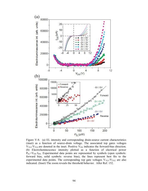
We also note that the onset of the forward-biased emission coincides with the current onset, while the onset of the reverse-biased emission lags behind the current onset. This is discussed in more detail for V-8 (b) inset below, and additionally in the investigation of electroluminescence width. It should be noted that we do not observe a significant influence of the split gate in the intensity characteristics of the emitted light in the reverse direction; on the negative VDS side, the intensity is almost identical for all the split-gate settings at any given VDS value. Although there is a potential drop between the top gates, the field created by the VTGS biasing does not appear to be greater than the impact excitation threshold, since there is little dependence on that parameter. In contrast, a single-tube device operated as a unipolar emitter shows a clear dependence on bottom global gate voltage (not shown), which is reasonable because the light generation depends of the degree of band bending at contacts that controls the carrier injection rate (see Figure IV-5 inset for schematics). From such split-gate effects and the differences between the forward and reverse biases, we can conclude that the CNT film device functions as a light- emitting diode. 93
(a) (b) Figure V-8. (a) EL intensity and corresponding drain-source current characteristics (inset) as a function of source-drain voltage. The associated top gates voltages VTG1/VTG2 are denoted in the inset. Positive VDS indicates the forward-bias direction. (b) Electroluminescence intensity plotted as a function of electrical power PEL=VDS·IDS. Experimental data points are represented by symbols (open symbols: forward bias, solid symbols: reverse bias), the lines represent best fits to the experimental data points. The corresponding top gate voltages VTG1/VTG2 are also indicated. (Inset) The zoom reveals the threshold behavior. After Ref. 152. 94
- Page 55 and 56: wetting with CNTs 57 and a relative
- Page 57 and 58: Figure III-4. (Main panel) Electrol
- Page 59 and 60: By plotting the current as a functi
- Page 61 and 62: phonon temperature in broadening. S
- Page 63 and 64: found multiple tubes bound together
- Page 65 and 66: where i is the phonon mode, Tsub is
- Page 67 and 68: The main panel of Figure III-10 sho
- Page 69 and 70: the effect following Perebeinos’
- Page 71 and 72: the optical phonon population is no
- Page 73 and 74: (a) Figure III-13. (a) Spectra from
- Page 75 and 76: DOP = I║ / (I┴ + I║) = 0.77.
- Page 77 and 78: inding energy for perpendicular exc
- Page 79 and 80: 3. Conclusions We have examined the
- Page 81 and 82: In a split-gate scheme, a new level
- Page 83 and 84: 3. Electroluminescence mechanism an
- Page 85 and 86: After calibrating our detection sys
- Page 87 and 88: (a) (b) Figure IV-3. Electrolumines
- Page 89 and 90: observed by increasing the VGS valu
- Page 91 and 92: We claimed in Chapter III that in t
- Page 93 and 94: Let us finally comment on the effic
- Page 95 and 96: Chapter V The Polarized Carbon Nano
- Page 97 and 98: (a) (b) Figure V-1. (a) SEM image o
- Page 99 and 100: oth electrons and holes can be inje
- Page 101 and 102: In the reverse direction (i.e., neg
- Page 103 and 104: 4. Electroluminescence characterist
- Page 105: and drain pads (marked “S” and
- Page 109 and 110: We attribute the observation of the
- Page 111 and 112: (a) (b) (c) Figure V-9. Electrolumi
- Page 113 and 114: measurements (i.e. additional chemi
- Page 115 and 116: (a) (b) Figure V-10. Full-width at
- Page 117 and 118: mechanisms are the same for differe
- Page 119 and 120: experiment, solid line: cosine squa
- Page 121 and 122: emission observed at higher current
- Page 123 and 124: Bibliography 1. Avouris, P.; Chen,
- Page 125 and 126: 30. Miyauchi, Y.; Maruyama, S., Ide
- Page 127 and 128: 56. Chen, Z.; Appenzeller, J.; Knoc
- Page 129 and 130: 85. Marty, L.; Adam, E.; Albert, L.
- Page 131 and 132: 112. Steiner, M.; Freitag, M.; Pere
- Page 133 and 134: 140. Grüneis, A.; Saito, R.; Samso
(a)<br />
(b)<br />
Figure V-8. (a) EL intensity and corresponding drain-source current characteristics<br />
(inset) as a function of source-drain voltage. The associated top gates voltages<br />
VTG1/VTG2 are denoted in the inset. Positive VDS indicates the forward-bias direction.<br />
(b) Electroluminescence intensity plotted as a function of electrical power<br />
PEL=VDS·IDS. Experimental data points are represented by symbols (open symbols:<br />
forward bias, solid symbols: reverse bias), the lines represent best fits to the<br />
experimental data points. The corresponding top gate voltages VTG1/VTG2 are also<br />
indicated. (Inset) The zoom reveals the threshold behavior. After Ref. 152.<br />
94


