MAC7100 Microcontroller Family Product Brief - Freescale ...
MAC7100 Microcontroller Family Product Brief - Freescale ...
MAC7100 Microcontroller Family Product Brief - Freescale ...

You also want an ePaper? Increase the reach of your titles
YUMPU automatically turns print PDFs into web optimized ePapers that Google loves.
<strong>Freescale</strong> Semiconductor<br />
<strong>Product</strong> <strong>Brief</strong><br />
<strong>MAC7100</strong> microcontrollers (MCUs) are members of a<br />
pin-compatible family of 32-bit Flash-memory-based<br />
devices developed specifically for embedded automotive<br />
applications. The pin-compatible family concept enables<br />
users to select between different memory and peripheral<br />
options for scalable designs. All <strong>MAC7100</strong> devices are<br />
composed of an ARM7TDMI-S 32-bit central<br />
processing unit, up to 1 Mbyte of high performance<br />
embedded Flash memory for program storage, an<br />
optional 32 Kbytes of embedded Flash for data and/or<br />
program storage, and up to 48 Kbytes of RAM.<br />
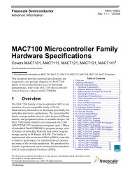
As shown in Table 1 and Figure 1, the <strong>MAC7100</strong> family<br />
is implemented with a variety of on-chip peripherals. An<br />
enhanced DMA (eDMA) controller executes in parallel<br />
with the CPU to improve the performance of data<br />
transfers between memory and many of the peripherals.<br />
DMA transfers may be triggered by various peripheral<br />
events, such as data frame transmission or reception,<br />
elapsed timer periods, and analog-to-data conversion<br />
completions. The peripheral set includes enhanced<br />
asynchronous serial communications interfaces (eSCI)<br />
with Local Interconnect Network (LIN) support<br />
hardware to reduce interrupt overhead, serial peripheral<br />
interfaces (DSPI) with flexible chip selects and fast baud<br />
This document contains information on a new product. Specifications and information herein<br />
are subject to change without notice.<br />
© <strong>Freescale</strong> Semiconductor, Inc., 2004. All rights reserved.<br />
• Preliminary<br />
<strong>MAC7100</strong>PB<br />
Rev. 2, 09/2004<br />
<strong>MAC7100</strong> <strong>Microcontroller</strong> <strong>Family</strong><br />
<strong>Product</strong> <strong>Brief</strong><br />
32-bit Embedded Controller Division<br />
1<br />
Table of Contents<br />
Block Diagram.........................................................3<br />
2 Features..................................................................4<br />
3 Modes of Operation ................................................8<br />
3.1 Chip Configuration Modes...................................8<br />
3.2 Low-Power Modes ...............................................9<br />
4 Functional Overview ...............................................9<br />
4.1 32-bit ARM7TDMI-S RISC Core..........................9<br />
4.2 Enhanced Direct Memory Access (eDMA) and<br />
Channel Multiplexer (DMA MUX) ......................10<br />
4.3 External Interface Module (EIM)........................10<br />
4.4 Common Flash Module (CFM) ..........................10<br />
4.5 Interrupt Controller (INTC).................................10<br />
4.6 Port Integration Module (PIM) ...........................11<br />
4.7 Analog-to-Digital Converters (ATD) ...................11<br />
4.8 CAN 2.0 Software Compatible (FlexCAN)<br />
Modules.............................................................12<br />
4.9 Enhanced Modular I/O Subsystem (eMIOS) .....12<br />
4.10 Serial Peripheral Interfaces (DSPI) ...................12<br />
4.11 Enhanced Serial Communications Interfaces<br />
(eSCI) ................................................................13<br />
4.12 Inter-Integrated Circuit (I 2C) Bus Module ..........13<br />
4.13 Periodic Interrupt Timer (PIT) Module ...............13<br />
4.14 Miscellaneous Control Module (MCM) and<br />
Cross-Bar Switch (XBS) ....................................13<br />
4.15 System Services Module (SSM)........................14<br />
4.16 Voltage Regulator Module (VREG)....................14<br />
4.17 System Clocks (OSC and CRG)......14<br />
4.18 Development Support......................15<br />
5 Documentation and Ordering..............15
ate switching, inter-integrated circuit (I 2 C) bus controllers, FlexCAN interfaces with flexible message<br />
buffering, an enhanced modular I/O subsystem (eMIOS) with sixteen high-performance 16-bit timers, one<br />
or two sixteen-channel 10-bit analog-to-digital converters (ATD), general-purpose timers (Programmable<br />
Interrupt Timer (PIT)) and two special-purpose timers (Real Time Interrupt (RTI) and Software Watchdog<br />
Timer (SWT)). The peripherals share a large number of general purpose input-output (GPIO) pins, all of<br />
which are bidirectional and available with interrupt capability to trigger wake-up from low-power chip<br />
modes.<br />
Internal data paths between the CPU core, eDMA, memory and peripherals are all 32 bits wide, further<br />
improving performance for 32-bit applications. Some devices also offer a 16-bit wide external data bus with<br />
22 address lines, allowing access of up to 4 MBytes of external address space. The inclusion of a programmable<br />
2<br />
Device<br />
Program Flash<br />
Data Flash<br />
SRAM<br />
External Bus<br />
ATD<br />
Modules (1)<br />
A<br />
B<br />
Table 1. <strong>MAC7100</strong> <strong>Family</strong> Device Derivatives<br />
A<br />
B<br />
CAN<br />
Modules<br />
C<br />
D<br />
A<br />
B<br />
eSCI<br />
Modules<br />
C<br />
D<br />
DSPI<br />
Modules (2)<br />
A<br />
B<br />
I 2 C Module<br />
eMIOS Module<br />
Timer Module<br />
<strong>MAC7100</strong> <strong>Microcontroller</strong> <strong>Family</strong> <strong>Product</strong> <strong>Brief</strong>, Rev. 2<br />
General-Purpose<br />
Input/Output Ports/Pins<br />
A B C D E F G H I<br />
MAC7101<br />
10 16 12 10 16 16 16 16 – 112 144 LQFP<br />
MAC7111 16 16 16 16 16 16 16 – – 112 144 LQFP<br />
MAC7121 (3) 10 15 1 11 16 16 16 – – 85 112 LQFP<br />
512 KBytes<br />
32 KBytes<br />
32 KBytes<br />
MAC7131 16 16 16 16 16 16 16 16 – 128 208 BGA<br />
MAC7141 4 16 – 10 16 16 10 – – 72 100 LQFP<br />
MAC7112<br />
16 16 16 16 16 16 16 – – 112 144 LQFP<br />
256 KBytes<br />
16 KBytes<br />
MAC7122 (3) 10 15 1 11 16 16 16 – – 85 112 LQFP<br />
MAC7142 4 16 – 10 16 16 10 – – 72 100 LQFP<br />
MAC7104<br />
10 16 12 10 16 16 16 16 112 144 LQFP<br />
384 KBytes<br />
24 KBytes<br />
16 channels, 16-bit<br />
10 channels, 24-bit<br />
MAC7114 16 16 16 16 16 16 16 – – 112 144 LQFP<br />
MAC7124 (3) 10 15 1 11 16 16 16 – – 85 112 LQFP<br />
MAC7134 16 16 16 16 16 16 16 16 – 128 208 BGA<br />
MAC7144 4 16 – 10 16 16 10 – – 72 100 LQFP<br />
MAC7105<br />
10 16 12 10 16 16 16 16 – 112 144 LQFP<br />
768 KBytes<br />
40 KBytes<br />
MAC7115 16 16 16 16 16 16 16 – – 112 144 LQFP<br />
MAC7125 (3) 10 15 1 11 16 16 16 – – 85 112 LQFP<br />
MAC7135 (4) (4) 16 16 16 16 16 16 16 16 16 144 208 BGA<br />
MAC7106<br />
10 16 12 10 16 16 16 16 – 112 144 LQFP<br />
1 MByte<br />
48 KBytes<br />
MAC7116 16 16 16 16 16 16 16 – – 112 144 LQFP<br />
MAC7126 (3) 10 15 1 11 16 16 16 – – 85 112 LQFP<br />
MAC7136 (4) (4) 16 16 16 16 16 16 16 16 16 144 208 BGA<br />
NOTES:<br />
1. 16 channels, 8/10-bit, per module.<br />
2. Up to four chip selects available per module, unless noted otherwise.<br />
3. Up to three chip selects available.<br />
4. Up to eight chip selects available.<br />
Preliminary <strong>Freescale</strong> Semiconductor<br />
Total (max.)<br />
Package
<strong>MAC7100</strong> <strong>Microcontroller</strong> <strong>Family</strong> <strong>Product</strong> <strong>Brief</strong>, Rev. 2<br />
Block Diagram<br />
PLL module allows power consumption and performance to be adjusted to suit operational requirements. Both<br />
E-ICE and Nexus 2 interfaces are implemented to support development and debug tool chains.<br />
<strong>MAC7100</strong> devices include an on-chip multi-output voltage regulator, thus requiring only a single external<br />
3.3V to 5V power supply. The maximum operating range of devices in the family covers a junction<br />
temperature of –40° C to 150° C and CPU clock frequencies up to 50 MHz (below 105° C, frequency is<br />
limited to 40 MHz @ 150° C). Packaging options range from 100-pin LQFP up to 208-pin MAP BGA.<br />
1 Block Diagram<br />
JTAG<br />
Standard <strong>Product</strong> Platform (SPP)<br />
E-ICE<br />
NEXUS II<br />
ARM7 TDMI-S<br />
FLASH Controller<br />
Program FLASH<br />
Data FLASH<br />
SRAM Controller<br />
SRAM<br />
EIM<br />
INTC<br />
Figure 1. <strong>MAC7100</strong> Device Block Diagram<br />
<strong>Freescale</strong> Semiconductor Preliminary<br />
3<br />
XBS<br />
VREG<br />
OSC & CRG<br />
SSM<br />
DMA MUX<br />
ATD A<br />
MCM<br />
eDMA<br />
AIPS<br />
Note: Refer to Table 1 for details of peripheral and memory configurations<br />
PIT<br />
PIM<br />
eMIOS<br />
ATD B<br />
Intelligent Peripheral<br />
Subsystem (IPS)<br />
I 2 C<br />
DSPI A<br />
DSPI B<br />
eSCI A<br />
eSCI B<br />
eSCI C<br />
eSCI D<br />
FlexCAN A<br />
FlexCAN B<br />
FlexCAN C<br />
FlexCAN D
Features<br />
2 Features<br />
As shown in Figure 1, <strong>MAC7100</strong> family devices are organized into two major blocks:<br />
• Standard <strong>Product</strong> Platform (SPP) — The SPP consists of the ARM7TDMI-S processor core and<br />
an enhanced direct memory access controller connected to a high-performance 32-bit bus through<br />
a cross-bar bus switch to the rest of the chip modules. The SPP also contains an interrupt<br />
controller, SRAM controller, Flash memory controller, external bus interface, peripheral bus<br />
bridge, and miscellaneous control module.<br />
• Intelligent Peripheral Subsystem (IPS) — The IPS consists of the voltage regulator, oscillator,<br />
clock and reset generator, port integration module, DMA request multiplexer, analog to digital<br />
converter(s), enhanced modular I/O subsystem, enhanced serial communications controllers,<br />
serial peripheral interfaces, FlexCAN controllers, an inter-integrated circuit (I 2 C) bus controller,<br />
programmable interrupt timer, and system services module.<br />
The primary features of <strong>MAC7100</strong> integrated processors include the following:<br />
• General <strong>MAC7100</strong> family features<br />
— Up to 50 MHz operating frequency<br />
— RISC core, eDMA, and memory connected via high performance 32-bit bus<br />
— Separate 32-bit bus interface for slower system peripherals<br />
— External bus interface available to support off-chip devices (on selected devices only)<br />
• 32-bit ARM7TDMI-S RISC core<br />
— Supports 32-bit and 16-bit (THUMB) instruction sets for code size efficiency<br />
— 32 bit wide data path<br />
— Alternate general-purpose registers<br />
— Byte (8-bit), halfword (16-bit), and word (32-bit) data types supported<br />
• Enhanced Direct Memory Access (eDMA) and Channel Multiplexer (DMA MUX)<br />
— Supports transfers between system memories, external devices, peripheral modules (ATD,<br />
DSPI, eMIOS, eSCI, and I 2 C), and general-purpose I/O using a dual-address transfer protocol<br />
— DMA MUX allows assignment of any DMA request source to any available eDMA channel<br />
— Programmable transfer control descriptors stored in local eDMA memory<br />
— Programmable source and destination address with configurable offset<br />
— Programmable transfer size and nesting via 32-bit major and 16-bit minor loop counters<br />
— Different final source and destination addresses allow circular queue operation<br />
— Programmable priority levels for each channel<br />
— Bandwidth control for each channel<br />
— Independently programmable read/write sizes<br />
— Periodic triggering of up to 8 channels<br />
• Memory options<br />
— Up to 1 Mbyte program Flash EEPROM<br />
– 50 MHz single-cycle non-sequential access for aligned halfword and aligned word data<br />
– State machine controlled program/erase operations<br />
– Internal programming voltage generator<br />
– Small Flash sector protection sizes<br />
– Configurable flexible Flash protection fields<br />
4<br />
<strong>MAC7100</strong> <strong>Microcontroller</strong> <strong>Family</strong> <strong>Product</strong> <strong>Brief</strong>, Rev. 2<br />
Preliminary<br />
<strong>Freescale</strong> Semiconductor
– Protection violation flag<br />
– 10,000 program / erase cycle endurance<br />
– 15-year data retention<br />
— 32 Kbyte data Flash EEPROM<br />
– 16-bit wide memory accessed via peripheral bus interface<br />
– Relocatable to page zero to provide data Flash boot operation<br />
– State machine controlled program/erase operations<br />
– Internal programming voltage generator<br />
– Up to 8 protected sectors in the data Flash<br />
– 10,000 program / erase cycle endurance<br />
– 15-year data retention<br />
— Up to 48 Kbyte RAM<br />
– Single cycle accesses to RAM for byte, halfword, and word reads and writes<br />
• Interrupt Controller (INTC)<br />
— 64 vectored interrupt sources<br />
— 44 peripheral, 17 DMA, 1 software watchdog timer, 2 external sources<br />
— 16 programmable interrupt priorities for every source, even in low-power modes<br />
— Multiple level interrupt nesting, with hardware support for first nesting level<br />
— Normal and Fast interrupt support<br />
• General purpose input/output<br />
— Up to 144 port pins shared with peripherals<br />
— All ports are 16 bits wide, with pins bidirectional and independently selectable<br />
— Wake-up interrupt available on all port pins<br />
• Analog-to-Digital Converter(s) (ATD)<br />
— One or two ATD modules<br />
— 16 analog input channels per ATD module<br />
— 10-bit resolution with ± 2 counts accuracy<br />
—7µS minimum conversion time<br />
— Internal sample and hold circuitry<br />
— Programmable input sample time for various source impedances<br />
— Queued conversion sequences supported by eDMA controller<br />
— Unused analog channels can be used as digital I/O<br />
— External and on-chip sample triggers, including periodic triggering via the PIT module<br />
— Synchronized sampling between ATD modules using external or on-chip triggers<br />
• CAN 2.0 software compatible modules (FlexCAN)<br />
— Up to four CAN modules<br />
— Full implementation of the CAN 2.0 protocol specification<br />
— Programmable bit rate up to 1M bps<br />
— Up to 32 flexible message buffers of 0 to 8 bytes data length for each module<br />
— All message buffers configurable for either Rx/Tx<br />
— Unused message buffer space can be used as general purpose RAM<br />
— Supports standard or extended messages<br />
— Time stamp, based on a 16-bit free-running counter<br />
<strong>MAC7100</strong> <strong>Microcontroller</strong> <strong>Family</strong> <strong>Product</strong> <strong>Brief</strong>, Rev. 2<br />
Features<br />
<strong>Freescale</strong> Semiconductor Preliminary<br />
5
Features<br />
6<br />
— Maskable interrupts, including low-power mode wake up on bus activity<br />
— Programmable I/O modes<br />
• Enhanced Modular I/O Subsystem (eMIOS)<br />
— 16 unified channels, each of which can be enabled for eDMA service<br />
— Three 16-bit counter buses, with synchronization between timebases<br />
— One global prescaler plus prescaler available on each channel<br />
— Channels can be individually disabled to assist with power saving<br />
— Fourteen channel operating modes available:<br />
– General-purpose input/output<br />
– Single-action input capture<br />
– Single-action output compare<br />
– Input pulse width measurement<br />
– Input period measurement<br />
– Double-action output compare<br />
– Pulse/edge accumulation<br />
– Pulse/edge counting<br />
– Quadrature decode<br />
– Windowed programmable time accumulation<br />
– Modulus counter<br />
– Output pulse width modulation<br />
– Output pulse width modulation, center aligned<br />
– Output pulse width and frequency modulation<br />
• Serial Peripheral Interfaces (DSPI)<br />
— Up to two DSPI modules<br />
— Full duplex, synchronous transfers<br />
— Master or slave operation<br />
— Programmable master bit rates<br />
— Programmable clock polarity and phase<br />
— End-of-transmission interrupt flag<br />
— Flexible baud rates available<br />
— Programmable data frames from 4 bits to 16 bits<br />
— Up to 8 chip select lines enable 256 external devices to be selected using external multiplexer<br />
— Two DMA request signals per module for message frame support<br />
— Separate transmit and receive FIFOs for improved system performance<br />
— Queueing operation possible through use of eDMA controller channels<br />
— Fast switching between SPI slave device types via transfer attributes coupled with data<br />
— General purpose I/O functionality on pins when not used for DSPI<br />
• Enhanced Serial Communications Interfaces (eSCI)<br />
— Up to four eSCI modules<br />
— Standard non-return-to-zero (NRZ) mark/space format<br />
— Full-duplex operation<br />
— Software selectable word length (8- or 9-bit words)<br />
— 10/11- or 13/14-bit break character formats available<br />
— 13-bit programmable baud-rate modulus counter<br />
<strong>MAC7100</strong> <strong>Microcontroller</strong> <strong>Family</strong> <strong>Product</strong> <strong>Brief</strong>, Rev. 2<br />
Preliminary<br />
<strong>Freescale</strong> Semiconductor
<strong>MAC7100</strong> <strong>Microcontroller</strong> <strong>Family</strong> <strong>Product</strong> <strong>Brief</strong>, Rev. 2<br />
Features<br />
— Separately enabled transmitter and receiver<br />
— Separate receiver and transmitter CPU interrupt requests<br />
— Programmable transmitter output polarity<br />
— Two receiver wake-up methods<br />
— Interrupt-driven operation with eight flags<br />
— Receiver framing error detection<br />
— Hardware parity checking<br />
— 1/16-bit time noise reduction<br />
— Two DMA request lines per module (one each for receive and transmit data)<br />
— Support for LIN bus protocol (version 1.2 and version 2.0).<br />
– Full LIN master node autonomous message frame handling.<br />
– Frame hardware significantly reduces interrupt overhead.<br />
– LIN message header generation.<br />
– Slave timeout detection.<br />
– Optional CRC message checking.<br />
– Detection and flagging of LIN errors.<br />
• Inter-Integrated Circuit (I 2 C) Bus module<br />
— Two wire bi-directional serial bus for on-board communications<br />
— Compatibility with I 2 C Bus standard<br />
— Multi-master operation<br />
— Software-programmable for one of 256 different serial clock frequencies<br />
— Interrupt-driven byte-by-byte data transfer<br />
— Arbitration-lost interrupt with automatic mode switching from master to slave<br />
— Calling address identification interrupt<br />
— Start and stop signal generation/detection<br />
— Repeated START signal generation<br />
— Acknowledge bit generation/detection<br />
— Bus-busy detection<br />
— Two DMA request lines to receive and transmit data<br />
• Periodic Interrupt Timer (PIT) Module<br />
— Independent timeout periods for each of the ten 24-bit timers<br />
— One real-time interrupt (RTI) timer to wake up the CPU in wait mode or pseudo-stop mode<br />
— Eight timers that can be configured to generate DMA trigger pulses<br />
— Four timers that can be configured to generate interrupts instead of triggers<br />
— Two timers that can be configured to generate ATD trigger pulses<br />
• Miscellaneous Control Module (MCM)<br />
— Program-visible information regarding the device configuration and revision<br />
— SPP module configuration and reset status<br />
— Software watchdog timer with programmable, staged response<br />
— Wake-up control for exiting sleep modes<br />
— Cross-bar switch remapping<br />
— Address information for faulted memory accesses<br />
<strong>Freescale</strong> Semiconductor Preliminary<br />
7
Modes of Operation<br />
8<br />
• System Services Module (SSM)<br />
— Memory sizes and status<br />
— Device mode and security status<br />
— eDMA status<br />
— Reserved address space protection<br />
— Debug status port configuration<br />
• Development support<br />
— Real-time instruction trace support via Nexus II interface<br />
— Selectable Nexus port position on 208-pin MAP BGA and 144-pin LQFP packaged device<br />
— ARM Embedded ICE debug interface<br />
— JTAG Test Access Port (TAP) interface<br />
— Debug mode access to CPU registers<br />
— Real Time memory access<br />
— Hardware Breakpoints<br />
• Clock generation<br />
— Selectable Standard Pierce or low-power Amplitude Loop Controlled (ALC) Pierce oscillator<br />
— Phase-locked loop clock frequency multiplier<br />
— Self-clocking mode available in absence of external clock<br />
— Low power 0.5 to 16 MHz crystal oscillator reference clock<br />
— Clock generation and monitor, reset control, and software watchdog timer (SWT)<br />
• I/O lines with 5 V input and drive capability, 5 V ATD converter inputs<br />
• 2.5 V logic supply, with internal 5 V to 2.5 V Regulator<br />
• 208-pin MAP BGA, 144-pin LQFP, 112-pin LQFP, and 100-pin LQFP package options<br />
3 Modes of Operation<br />
3.1 Chip Configuration Modes<br />
Devices in the MAC700 family operate in several different modes, depending on the particular application<br />
and stage of development. There are 6 modes available for <strong>MAC7100</strong> devices, as determined via external<br />
input during reset as well as the security state of the on-chip program Flash memory. The selected mode<br />
affects the memory map, debug features, and security features:<br />
• Normal Single-Chip Mode<br />
— All debug features available<br />
— Boot from program Flash<br />
• Normal Expanded Mode<br />
— All debug features available<br />
— Boot from off-chip device using the external bus interface<br />
— Program and data Flash memory available<br />
• Secured Single-Chip Mode<br />
— No debug features available<br />
— No external bus interface<br />
<strong>MAC7100</strong> <strong>Microcontroller</strong> <strong>Family</strong> <strong>Product</strong> <strong>Brief</strong>, Rev. 2<br />
Preliminary<br />
<strong>Freescale</strong> Semiconductor
— Boot from program Flash<br />
— JTAG lockout recovery available<br />
• Secured Expanded Mode<br />
— All debug features available.<br />
— Boot from off-chip device using the external bus interface<br />
— Program and data Flash memory not available<br />
• Data Flash Boot Mode<br />
— All debug features available<br />
— Boot from data Flash<br />
• Secured Data Flash Boot Mode<br />
— No debug features available<br />
— No external bus interface<br />
— Boot from data Flash<br />
— JTAG lockout recovery available<br />
3.2 Low-Power Modes<br />
<strong>MAC7100</strong> <strong>Microcontroller</strong> <strong>Family</strong> <strong>Product</strong> <strong>Brief</strong>, Rev. 2<br />
Functional Overview<br />
There are three low-power modes available:<br />
• Stop Mode (provides the lowest power consumption)<br />
This is a mode in which all MCU clocks are stopped for maximum power savings. Typically, when<br />
stop mode is requested, each module puts itself in a known state and then sends a stop acknowledge<br />
signal to inform the clock module that it can stop the clocks.<br />
• Pseudo-Stop Mode<br />
The oscillator continues to run and most of the system and peripheral clocks are stopped. If the<br />
respective enable bits are set, the SWT and RTI will continue to run, otherwise they also stop.<br />
• Doze Mode<br />
This is a mode in which the CPU bus is kept alive and a global doze mode request is sent to all<br />
peripherals asking them to enter low power mode. Typically, when doze mode is requested, each<br />
peripheral can be enabled to enter low power mode or continue normal operation.<br />
4 Functional Overview<br />
The following is a brief summary of the functional blocks in the <strong>MAC7100</strong> devices. For more details refer<br />
to the <strong>MAC7100</strong> <strong>Microcontroller</strong> <strong>Family</strong> Reference Manual (<strong>MAC7100</strong>RM).<br />
4.1 32-bit ARM7TDMI-S RISC Core<br />
The <strong>MAC7100</strong> family is implemented with an ARM7 CPU. This is a 32-bit RISC core with a three-stage<br />
pipeline for high instruction throughput. The core used across the family is the ARM7TDMI-S, which<br />
supports both 32-bit and 16-bit (THUMB) instruction sets for optimum code density. No architectural<br />
modifications have been made to this core during implementation, enabling the <strong>MAC7100</strong> family to<br />
remain compliant to the ARM ISA V4T and existing tool chains. The core is implemented to support big<br />
endian memory systems.<br />
<strong>Freescale</strong> Semiconductor Preliminary<br />
9
Functional Overview<br />
4.2 Enhanced Direct Memory Access (eDMA) and<br />
Channel Multiplexer (DMA MUX)<br />
The implementation of the eDMA on the <strong>MAC7100</strong> family is targeted towards cost-sensitive applications<br />
while providing a high level of functionality. The eDMA executes in parallel with the CPU, which enables<br />
transfers of data between the memory, peripherals, and off-chip devices with little intervention from the<br />
core; thus increasing system performance as well as simplifying software development. The eDMA is<br />
capable of performing complex data transfers with minimal intervention from a host processor via 16<br />
programmable DMA channels. The hardware microarchitecture includes the eDMA engine (which<br />
performs source / destination address calculations and data movement operations), and a dedicated<br />
memory array containing transfer control descriptors. The SRAM-based implementation is utilized to<br />
minimize overall module size.<br />
4.3 External Interface Module (EIM)<br />
The EIM connects the device to off-chip resources and is not available in all <strong>MAC7100</strong> packages. Two<br />
components make up this module: a user-programmable chip select module and the bus controller. The bus<br />
controller uses a simple, flexible bus protocol that supports a variety of external memory devices with little<br />
or no external logic needed, and is based on the external bus of the 68K/Coldfire® family of devices. All<br />
transfers on the external bus are controlled by the MCU masters (CPU or eDMA).<br />
The EIM supports a normal three clock-cycle access, but a two cycle fast termination can also be used if<br />
the transfer acknowledge signal is asserted before the rising edge of the second CLKOUT cycle. The EIM<br />
also provides support for burst transfers of up to 16 bytes of data with the proper external support logic.<br />
4.4 Common Flash Module (CFM)<br />
The CFM provides up to 1 Mbyte of 32-bit program Flash memory and 32 Kbytes of 16-bit data Flash<br />
memory. The Flash memory serves as electrically erasable and programmable, non-volatile memory. It is<br />
ideal for program and data storage for single-chip applications allowing for field reprogramming without<br />
requiring external programming voltage sources. For more information on the non-volatile memory<br />
options on <strong>MAC7100</strong> devices, refer to Table 1.<br />
4.5 Interrupt Controller (INTC)<br />
<strong>MAC7100</strong> family devices implement an Interrupt Controller (INTC) Module which supports 64 interrupt<br />
requests. The INTC is a highly-programmable controller, collecting interrupt requests, mapping the<br />
requests into 16 priority levels, and then signalling the ARM processor when a properly enabled unmasked<br />
request is active. In response to the service routine’s memory mapped interrupt acknowledge read cycle,<br />
the INTC returns a unique vector for each interrupt request and automatically manages masking of lower<br />
level requests. As any interrupt source can be assigned to any of the sixteen priority levels, and the INTC<br />
enables the definition of which priority levels are assigned to fast or normal interrupts, each interrupt<br />
source can be selected to generate either a fast or normal interrupt to the core by its assigned level.<br />
10<br />
<strong>MAC7100</strong> <strong>Microcontroller</strong> <strong>Family</strong> <strong>Product</strong> <strong>Brief</strong>, Rev. 2<br />
Preliminary<br />
<strong>Freescale</strong> Semiconductor
4.6 Port Integration Module (PIM)<br />
<strong>MAC7100</strong> <strong>Microcontroller</strong> <strong>Family</strong> <strong>Product</strong> <strong>Brief</strong>, Rev. 2<br />
Functional Overview<br />
The Port Integration Module (PIM) provides the interface between the physical pins and either the general<br />
purpose I/O signals or the various peripherals which provide alternate signal functions. <strong>MAC7100</strong> devices<br />
implement up to 9 ports, each of which is up to 16-bits wide (all pins are not available in some packages).<br />
Each pin can be independently configured to be either in port mode or peripheral mode. When peripheral<br />
mode is selected, the pin’s output and configuration are both controlled by the peripheral module. Each pin<br />
is also capable of being used as an interrupt source with a filter available to help eliminate instances of<br />
noise-generated false interrupts. For some devices, GPIO Port H is available rather than Port C; the PIM<br />
enables swapping of Port H and Port C in the address map to assist transparent porting of code between<br />
various devices. Following a reset into any mode other than normal or secured expanded mode, all pins are<br />
configured as general purpose inputs. Following a reset into normal or secured expanded mode, some pins<br />
are controlled by the External Interface Module (EIM) and are not available for general purpose functions.<br />
In order to improve software performance, all pins can be controlled either in a port-wise or bit-wise<br />
manner in general purpose I/O mode. Registers are provided which allow each pin to be independently<br />
controlled by writing to a separate register. Mirror registers are also available to simplify read and write<br />
operations by accessing all pins in a port at one time.<br />
4.7 Analog-to-Digital Converters (ATD)<br />
The Analog-to-Digital Converter (ATD) Module is a 16-channel, multiplexed input, successive<br />
approximation analog-to-digital converter with a programmable resolution of 8 or 10 bits. <strong>MAC7100</strong><br />
devices implement one or two Analog to Digital (ATD) Converter modules; refer to Table 1 for the ATD<br />
configuration of a specific device.<br />
The ATD modules may be serviced by the eDMA in order to improve overall system performance. Two<br />
DMA request channels may be used by each of the ATDs (on devices with two ATDs): one channel per<br />
ATD to move conversion command words to the ATD command registers, and one channel per ATD to<br />
move conversion results out of the ATD result registers.The conversion command word is used to define<br />
parameters such as the mode of conversion, the channel to be converted and the length of the conversion.<br />
By defining a number of conversion words in the MCUs system memory, it is possible to build a<br />
predefined sequence of conversions which will be executed without the intervention of the CPU. It is also<br />
possible for the CPU to write the conversion command word and to read the conversion results directly<br />
without the need to use the eDMA.<br />
<strong>MAC7100</strong> ATD modules include the ability to trigger a conversion sequence based on either an external<br />
signal or by one of two internal signals, SYSTRG0 or SYSTRG1. In order to use an external trigger source<br />
to initiate a conversion, any one of the analog channels can be used as an off-chip trigger. The internal<br />
trigger signal lines are connected to the Programmable Interrupt Timer (PIT), which provides two<br />
dedicated programmable 24-bit timers to trigger the ATD. The counter associated with the SYSTRGn<br />
signals can be programmed with the desired conversion trigger periods. This counter will count down from<br />
the preloaded value to zero at the rate defined by the system clock frequency. When the counter reaches<br />
zero the trigger signal is asserted to the ATD, then it is reloaded and the count down continues. For those<br />
devices that implement two ATD modules, when it is necessary to perform synchronous conversion by<br />
both, ATD_A and ATD_B can use the same external source, with one channel from each module assigned<br />
as the input for this trigger. Alternatively, both modules can use the same internal system trigger.<br />
<strong>Freescale</strong> Semiconductor Preliminary<br />
11
Functional Overview<br />
4.8 CAN 2.0 Software Compatible (FlexCAN) Modules<br />
There are up to four FlexCAN modules on <strong>MAC7100</strong> devices; refer to Table 1 for the number of FlexCAN<br />
channels implemented on a specific device. The CAN protocol is primarily, but not only, designed to be<br />
used as a vehicle serial data bus, meeting the specific requirements of this application: real-time processing,<br />
reliable operation in the EMI environment of a vehicle, cost-effectiveness, and required bandwidth. The<br />
FlexCAN module is a full implementation of the CAN protocol specification, Version 2.0 B, which<br />
supports both standard and extended message frames. A flexible number of message buffers (up to 32 MBs)<br />
is also supported, which are stored in an embedded RAM dedicated to the FlexCAN module (up to 544<br />
bytes capability).<br />
On <strong>MAC7100</strong> devices, the clock source for the FlexCAN can be selected to be derived either from the PLL<br />
clock or the oscillator clock. The FlexCAN also implements a low pass filter which can be used to wake<br />
up the device when activity is detected on the bus, while also enabling rejection of bus noise to help<br />
eliminate instances of false wake. <strong>MAC7100</strong> devices implement 32 mailboxes on each CAN module.<br />
4.9 Enhanced Modular I/O Subsystem (eMIOS)<br />
The Enhanced Modular I/O Subsystem (eMIOS) provides functionality to generate or measure time-based<br />
events. The eMIOS module implemented on <strong>MAC7100</strong> family devices has 16 unified timer channels<br />
(UCs), each with a 16-bit counter. Each UC is identical and can be configured to provide a wide range of<br />
timer functions. The module implements 3 counter busses for inter-channel synchronization and sharing<br />
common time bases.<br />
Each of the UCs has a single input/output signal associated with it, resulting in a module with 16 external<br />
signals available for the user. The eMIOS module can be independently disabled. Disabling the module<br />
turns off the clock to the module, although some of the module registers remain available to be accessed<br />
by the core via the peripheral bus.<br />
4.10 Serial Peripheral Interfaces (DSPI)<br />
<strong>MAC7100</strong> devices implement up to two (Deserial) Serial Peripheral Interface modules (DSPI). Only the<br />
SPI configuration is implemented in the <strong>MAC7100</strong> family of devices. Refer to Table 1 for the number of<br />
DSPI channels implemented on a specific device. Each DSPI supports up to eight peripheral chip select<br />
lines, offering selection of up to 8 external devices without external hardware, expandable to 256 with an<br />
external demultiplexer. One of the chip select signals can be used to provide a strobe for the other chip<br />
selects in order to eliminate decoding glitches generated when the chip selects change. This allows<br />
glitch-free selection of up to 128 external devices via external hardware.<br />
The DSPI is implemented with separate transmit and receive FIFOs with a depth of up to four entries.<br />
These FIFOs can be accessed either by the CPU or the eDMA to enable queued operations to be performed.<br />
Each DSPI has a separate DMA request channel for the transmit and the receive sides of the module. For<br />
queued operations the SPI queues reside in system RAM external to the DSPI. Data transfers between the<br />
queues and the DSPI FIFOs are accomplished through the use of the eDMA controller or through host<br />
software. Each queue entry contains both configuration information and data, enabling fast baud rate and<br />
chip select switching between frames with no CPU overhead and no SPI channel dead time.<br />
12<br />
<strong>MAC7100</strong> <strong>Microcontroller</strong> <strong>Family</strong> <strong>Product</strong> <strong>Brief</strong>, Rev. 2<br />
Preliminary<br />
<strong>Freescale</strong> Semiconductor
<strong>MAC7100</strong> <strong>Microcontroller</strong> <strong>Family</strong> <strong>Product</strong> <strong>Brief</strong>, Rev. 2<br />
Functional Overview<br />
4.11 Enhanced Serial Communications Interfaces (eSCI)<br />
There are up to four Enhanced Serial Communications Interfaces (eSCI) implemented on <strong>MAC7100</strong><br />
devices. Refer to Table 1 for the number of eSCI channels implemented on a specific device. The eSCI<br />
provides full duplex, asynchronous, NRZ serial communication with remote devices, including other<br />
MPUs. The eSCI transmitter and receiver operate independently, although they use the same baud rate<br />
generator. The CPU monitors the status of the eSCI, writes the data to be transmitted, and processes<br />
received data. The enhancement offered by this module over other <strong>Freescale</strong> SCIs is the inclusion of<br />
additional features which support a Local Interconnect Network (LIN) bus master, and complies with the<br />
LIN 2.0 specification. LIN master mode enables handling message frames rather than individual data<br />
packets, thus significantly reducing interrupt overhead (for example, from 13 individual interrupts to one).<br />
4.12 Inter-Integrated Circuit (I 2 C) Bus Module<br />
The Inter-Integrated Circuit Bus (I 2 C or IIC) is a two-wire bidirectional serial bus that provides a simple<br />
and efficient method of data exchange between devices. It minimizes the number of external connections<br />
between devices and does not require an external address decoder. The I 2 C bus is suitable for applications<br />
requiring occasional communications over a short distance between a number of devices. It also provides<br />
flexibility, allowing additional devices to be connected to the bus for further expansion and system<br />
development. The interface is designed to operate at up to 100 Kbps with maximum bus loading and<br />
timing. <strong>MAC7100</strong> family devices are capable of operating at higher baud rates, up to a maximum of the<br />
module clock divided by 20, with reduced bus loading. The maximum communication length and the<br />
number of devices that can be connected are limited by the maximum bus capacitance of 400 pF.<br />
4.13 Periodic Interrupt Timer (PIT) Module<br />
The PIT is an array of timers that can be used to generate interrupts and trigger eDMA channels. It also<br />
provides a dedicated Real-Time Interrupt (RTI) timer, which runs on a separate clock and can be used for<br />
system wake-up from low-power modes.<br />
The PIT provides eleven programmable timers offering a range of functions. All of the timers are 24-bit<br />
wide down-counters. Once zero is reached, a trigger can be generated, then the counter is reloaded with<br />
the start value and continues to be decremented. The value of the decrementer can be read at any time. The<br />
eleven timers provide one Real Time Interrupt (RTI), four general purpose timers, four eDMA trigger<br />
timers, and two timers used to trigger ATD conversions.<br />
4.14 Miscellaneous Control Module (MCM) and Cross-Bar<br />
Switch (XBS)<br />
The Miscellaneous Control Module (MCM) provides several control functions for the <strong>MAC7100</strong> family<br />
Standard <strong>Product</strong> Platform (SPP), including program-visible information regarding configuration and<br />
revision levels, a reset status register, a software watchdog timer, wake-up control for exiting sleep modes,<br />
the control registers for the crossbar switch, and generic access error information for the processor core.<br />
<strong>Freescale</strong> Semiconductor Preliminary<br />
13
Functional Overview<br />
The software watchdog timer (SWT) is contained within the MCM and supports either interrupt or reset<br />
generation on the occurrence of a time-out event. The SWT also supports a windowed time period,<br />
requiring the writing of the watchdog key within a specified time window. The source for the SWT clock<br />
is controlled by the clock and reset generator module (CRG).<br />
The MCM also configures the crossbar switch (XBS) address map to steer access to the crossbar slave<br />
ports in order to provide remapping operations. Following reset, the mapping is determined by the chip<br />
mode entered. Following reset the Flash, external bus, and RAM can be remapped as necessary.<br />
4.15 System Services Module (SSM)<br />
The SSM contains information on device configuration and the status of the eDMA controller.<br />
4.16 Voltage Regulator Module (VREG)<br />
The voltage regulator (VREG) module provides the internal voltage for the on-chip logic, which enables<br />
devices in the <strong>MAC7100</strong> family to be supplied with a single 5V power supply source. The VREG module<br />
is a dual output voltage regulator providing two 2.5 V (typical) supplies that differ in the amount of current<br />
that can be sourced by each. The regulator input voltage range is from 3.3 V up to 5 V. In low-power modes<br />
of operation the voltage regulator output can be reduced in order to further assist with power saving. The<br />
VREG can also be shut down by connecting the V DD R pin to V SS R.<br />
4.17 System Clocks (OSC and CRG)<br />
The Pierce oscillator (OSC) coupled with the Clock and Reset Generator (CRG) provide the internal clock<br />
signals for the core and all peripheral modules. The system clock can be supplied to the MCU in several<br />
ways, enabling support for a range of system operating frequencies:<br />
• From the oscillator, with a frequency set by an external, 16 MHz maximum, crystal reference<br />
• From the on-chip phase-locked loop, using the oscillator clock as a reference<br />
• From the PLL in self-clocking mode<br />
The clock generated by the oscillator or the phase-locked loop (PLL) provides the main system clock<br />
frequency, fSYS . The system clock is used throughout the device to drive the core and the memories. The<br />
IPS peripherals use a clock equal to fSYS ÷ 2.<br />
The program Flash memory is supplied by both fSYS and fSYS ÷ 2. fSYS is used for access to the Flash<br />
controller, but the interleaved Flash arrays operate at half the system frequency to allow enough time to<br />
access the array, enabling the memory controller to achieve close to single-cycle access times.<br />
The CAN modules may be configured to utilize either the peripheral clock (fSYS ÷ 2) or the oscillator clock<br />
(OSCCLK). This allows the user to select the CAN clock based on the required jitter performance.<br />
The Periodic Interrupt Timer (PIT) and Software Watchdog Timer (SWT) can be configured to run from<br />
the oscillator or the PLL generated clock. This allows these functions to continue to run during low-power<br />
operating modes if required.<br />
14<br />
<strong>MAC7100</strong> <strong>Microcontroller</strong> <strong>Family</strong> <strong>Product</strong> <strong>Brief</strong>, Rev. 2<br />
Preliminary<br />
<strong>Freescale</strong> Semiconductor
4.18 Development Support<br />
<strong>MAC7100</strong> <strong>Microcontroller</strong> <strong>Family</strong> <strong>Product</strong> <strong>Brief</strong>, Rev. 2<br />
Documentation and Ordering<br />
The <strong>MAC7100</strong> family of devices offers debugging with the EmbeddedICE (E-ICE) and a NEXUS 2 Plus<br />
interface. EmbeddedICE offers debug features such as setting breakpoints or watchpoints, modifying and<br />
reading memory contents. EmbeddedICE uses the standard JTAG serial interface and Test Access Port<br />
(TAP) and is compatible with existing ARM tool chains. The NEXUS interface provides real-time<br />
program trace capability and also uses the JTAG port, while also providing an auxiliary port for additional<br />
debug capabilities. The auxiliary port can be provided in two pin positions depending on the device and<br />
package. In the 208 MAP BGA and 144 LQFP package, it is possible for the NEXUS port to be available<br />
on either the low byte of Port A or the low byte of Port E. On smaller packages, the Nexus port is available<br />
only in the Port E position.<br />
5 Documentation and Ordering<br />
Table 2 lists the documents that provide a complete description of the <strong>MAC7100</strong> microcontroller family<br />
and are required to design properly with devices in the family. Documentation is available from a local<br />
<strong>Freescale</strong> Semiconductor sales office or distributor, the <strong>Freescale</strong> Literature Distribution Center, or<br />
through the <strong>Freescale</strong> web site at http://www.freescale.com. Figure 2 shows an example orderable part<br />
number and description that is used to completely specify a <strong>MAC7100</strong> family device.<br />
Table 2. <strong>MAC7100</strong> <strong>Family</strong> Documentation<br />
Document Name Order Number<br />
<strong>MAC7100</strong> <strong>Microcontroller</strong> <strong>Family</strong> Reference Manual <strong>MAC7100</strong>RM<br />
<strong>MAC7100</strong> Hardware Specifications <strong>MAC7100</strong>EC<br />
ARM Architecture Reference Manual (Second Edition) ARM DDI 0100E<br />
ARM7TDMI-S (Rev 4) Technical Reference Manual (Issue A) ARM DDI 0234A<br />
LIN Specification 2.0<br />
CAN protocol specification, Version 2.0 B<br />
Qualification Status 00<br />
Core Code 00<br />
Core Number 00<br />
Generation / <strong>Family</strong> 00<br />
Package Option (1)<br />
FU = 100 LQFP<br />
PV = 112 / 144 LQFP<br />
VF = 208 MAP BGA<br />
M AC 7 1 0 1 C PV 50 xx<br />
1. Package Option 2. Temperature Option<br />
C = –40°C to 85°C<br />
V = –40°C to 105°C<br />
M = –40°C to 125°C<br />
Figure 2. Orderable Part Number Example<br />
Optional Package Identifiers<br />
Speed (MHz)<br />
Package Identifier<br />
Temperature Range (2)<br />
Device Number<br />
<strong>Freescale</strong> Semiconductor Preliminary<br />
15
How to Reach Us:<br />
Home Page:<br />
www.freescale.com<br />
E-mail:<br />
support@freescale.com<br />
USA/Europe or Locations Not Listed:<br />
<strong>Freescale</strong> Semiconductor<br />
Technical Information Center, CH370<br />
1300 N. Alma School Road<br />
Chandler, Arizona 85224<br />
+1-800-521-6274 or +1-480-768-2130<br />
support@freescale.com<br />
Europe, Middle East, and Africa:<br />
<strong>Freescale</strong> Halbleiter Deutschland GmbH<br />
Technical Information Center<br />
Schatzbogen 7<br />
81829 Muenchen, Germany<br />
+44 1296 380 456 (English)<br />
+46 8 52200080 (English)<br />
+49 89 92103 559 (German)<br />
+33 1 69 35 48 48 (French)<br />
support@freescale.com<br />
Japan:<br />
<strong>Freescale</strong> Semiconductor Japan Ltd.<br />
Technical Information Center<br />
3-20-1, Minami-Azabu, Minato-ku<br />
Tokyo 106-0047, Japan<br />
0120 191014 or +81 3 3440 3569<br />
support.japan@freescale.com<br />
Asia/Pacific:<br />
<strong>Freescale</strong> Semiconductor Hong Kong Ltd.<br />
Technical Information Center<br />
2 Dai King Street<br />
Tai Po Industrial Estate<br />
Tai Po, N.T., Hong Kong<br />
+800 2666 8080<br />
support.asia@freescale.com<br />
For Literature Requests Only:<br />
<strong>Freescale</strong> Semiconductor Literature Distribution Center<br />
P.O. Box 5405<br />
Denver, Colorado 80217<br />
1-800-441-2447 or 303-675-2140<br />
Fax: 303-675-2150<br />
LDCFor<strong>Freescale</strong>Semiconductor@hibbertgroup.com<br />
Information in this document is provided solely to enable system and<br />
software implementers to use <strong>Freescale</strong> Semiconductor products. There are<br />
no express or implied copyright licenses granted hereunder to design or<br />
fabricate any integrated circuits or integrated circuits based on the<br />
information in this document.<br />
<strong>Freescale</strong> Semiconductor reserves the right to make changes without further<br />
notice to any products herein. <strong>Freescale</strong> Semiconductor makes no warranty,<br />
representation or guarantee regarding the suitability of its products for any<br />
particular purpose, nor does <strong>Freescale</strong> Semiconductor assume any liability<br />
arising out of the application or use of any product or circuit, and specifically<br />
disclaims any and all liability, including without limitation consequential or<br />
incidental damages. “Typical” parameters that may be provided in <strong>Freescale</strong><br />
Semiconductor data sheets and/or specifications can and do vary in different<br />
applications and actual performance may vary over time. All operating<br />
parameters, including “Typicals”, must be validated for each customer<br />
application by customer’s technical experts. <strong>Freescale</strong> Semiconductor does<br />
not convey any license under its patent rights nor the rights of others.<br />
<strong>Freescale</strong> Semiconductor products are not designed, intended, or authorized<br />
for use as components in systems intended for surgical implant into the body,<br />
or other applications intended to support or sustain life, or for any other<br />
application in which the failure of the <strong>Freescale</strong> Semiconductor product could<br />
create a situation where personal injury or death may occur. Should Buyer<br />
purchase or use <strong>Freescale</strong> Semiconductor products for any such unintended<br />
or unauthorized application, Buyer shall indemnify and hold <strong>Freescale</strong><br />
Semiconductor and its officers, employees, subsidiaries, affiliates, and<br />
distributors harmless against all claims, costs, damages, and expenses, and<br />
reasonable attorney fees arising out of, directly or indirectly, any claim of<br />
personal injury or death associated with such unintended or unauthorized<br />
use, even if such claim alleges that <strong>Freescale</strong> Semiconductor was negligent<br />
regarding the design or manufacture of the part.<br />
<strong>Freescale</strong> and the <strong>Freescale</strong> logo are trademarks of <strong>Freescale</strong><br />
Semiconductor, Inc. All other product or service names are the property<br />
of their respective owners. The ARM POWERED logo is a registered<br />
trademark of ARM Limited. ARM7TDMI-S is a trademark of ARM Limited.<br />
© <strong>Freescale</strong> Semiconductor, Inc. 2004. All rights reserved.<br />
<strong>MAC7100</strong>PB<br />
Rev. 2<br />
09/2004