Brushless DC Motor Control Made Easy - Microchip
Brushless DC Motor Control Made Easy - Microchip
Brushless DC Motor Control Made Easy - Microchip

You also want an ePaper? Increase the reach of your titles
YUMPU automatically turns print PDFs into web optimized ePapers that Google loves.
Author: Ward Brown<br />
<strong>Microchip</strong> Technology Inc.<br />
INTRODUCTION<br />
This application note discusses the steps of developing<br />
several controllers for brushless motors. We cover sensored,<br />
sensorless, open loop, and closed loop design.<br />
There is even a controller with independent voltage and<br />
speed controls so you can discover your motor’s characteristics<br />
empirically.<br />
The code in this application note was developed with<br />
the <strong>Microchip</strong> PIC16F877 PICmicro ® Microcontroller, in<br />
conjuction with the In-Circuit Debugger (ICD). This<br />
combination was chosen because the ICD is inexpensive,<br />
and code can be debugged in the prototype hardware<br />
without need for an extra programmer or<br />
emulator. As the design develops, we program the tar-<br />
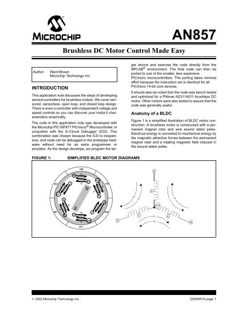
FIGURE 1: SIMPLIFIED BL<strong>DC</strong> MOTOR DIAGRAMS<br />
101<br />
001<br />
com<br />
S<br />
<strong>Brushless</strong> <strong>DC</strong> <strong>Motor</strong> <strong>Control</strong> <strong>Made</strong> <strong>Easy</strong><br />
b<br />
B<br />
N<br />
c<br />
A<br />
S<br />
a<br />
100<br />
N<br />
com<br />
a<br />
S 110<br />
N<br />
S<br />
011<br />
N<br />
com<br />
c<br />
S<br />
b<br />
N<br />
C<br />
010<br />
C<br />
AN857<br />
get device and exercise the code directly from the<br />
MPLAB ® environment. The final code can then be<br />
ported to one of the smaller, less expensive,<br />
PICmicro microcontrollers. The porting takes minimal<br />
effort because the instruction set is identical for all<br />
PICmicro 14-bit core devices.<br />
It should also be noted that the code was bench tested<br />
and optimized for a Pittman N2311A011 brushless <strong>DC</strong><br />
motor. Other motors were also tested to assure that the<br />
code was generally useful.<br />
Anatomy of a BL<strong>DC</strong><br />
Figure 1 is a simplified illustration of BL<strong>DC</strong> motor construction.<br />
A brushless motor is constructed with a permanent<br />
magnet rotor and wire wound stator poles.<br />
Electrical energy is converted to mechanical energy by<br />
the magnetic attractive forces between the permanent<br />
magnet rotor and a rotating magnetic field induced in<br />
the wound stator poles.<br />
© 2002 <strong>Microchip</strong> Technology Inc. DS00857A-page 1<br />
6<br />
3<br />
c<br />
a<br />
A<br />
2<br />
5<br />
com<br />
b<br />
1<br />
4<br />
B
AN857<br />
In this example there are three electromagnetic circuits<br />
connected at a common point. Each electromagnetic<br />
circuit is split in the center, thereby permitting the permanent<br />
magnet rotor to move in the middle of the<br />
induced magnetic field. Most BL<strong>DC</strong> motors have a<br />
three-phase winding topology with star connection. A<br />
motor with this topology is driven by energizing 2<br />
phases at a time. The static alignment shown in<br />
Figure 2, is that which would be realized by creating an<br />
electric current flow from terminal A to B, noted as path<br />
1 on the schematic in Figure 1. The rotor can be made<br />
to rotate clockwise 60 degrees from the A to B alignment<br />
by changing the current path to flow from terminal<br />
C to B, noted as path 2 on the schematic. The suggested<br />
magnetic alignment is used only for illustration<br />
purposes because it is easy to visualize. In practice,<br />
maximum torque is obtained when the permanent magnet<br />
rotor is 90 degrees away from alignment with the<br />
stator magnetic field.<br />
The key to BL<strong>DC</strong> commutation is to sense the rotor<br />
position, then energize the phases that will produce the<br />
most amount of torque. The rotor travels 60 electrical<br />
degrees per commutation step. The appropriate stator<br />
current path is activated when the rotor is 120 degrees<br />
from alignment with the corresponding stator magnetic<br />
field, and then deactivated when the rotor is 60 degrees<br />
from alignment, at which time the next circuit is activated<br />
and the process repeats. Commutation for the<br />
rotor position, shown in Figure 1, would be at the completion<br />
of current path 2 and the beginning of current<br />
path 3 for clockwise rotation. Commutating the electri-<br />
FIGURE 2: SENSOR VERSUS DRIVE TIMING<br />
A<br />
B<br />
C<br />
Sensor A<br />
Sensor B<br />
+V<br />
Float<br />
-V<br />
+V<br />
Float<br />
-V<br />
+V<br />
Float<br />
Sensor C<br />
-V<br />
H<br />
L<br />
H<br />
L<br />
H<br />
L<br />
...1<br />
cal connections through the six possible combinations,<br />
numbered 1 through 6, at precisely the right moments<br />
will pull the rotor through one electrical revolution.<br />
In the simplified motor of Figure 1, one electrical revolution<br />
is the same as one mechanical revolution. In<br />
actual practice, BL<strong>DC</strong> motors have more than one of<br />
the electrical circuits shown, wired in parallel to each<br />
other, and a corresponding multi-pole permanent magnetic<br />
rotor. For two circuits there are two electrical revolutions<br />
per mechanical revolution, so for a two circuit<br />
motor, each electrical commutation phase would cover<br />
30 degrees of mechanical rotation.<br />
Sensored Commutation<br />
The easiest way to know the correct moment to commutate<br />
the winding currents is by means of a position<br />
sensor. Many BL<strong>DC</strong> motor manufacturers supply<br />
motors with a three-element Hall effect position sensor.<br />
Each sensor element outputs a digital high level for 180<br />
electrical degrees of electrical rotation, and a low level<br />
for the other 180 electrical degrees. The three sensors<br />
are offset from each other by 60 electrical degrees so<br />
that each sensor output is in alignment with one of the<br />
electromagnetic circuits. A timing diagram showing the<br />
relationship between the sensor outputs and the<br />
required motor drive voltages is shown in Figure 2.<br />
6 5 4 3 2 1 6...<br />
Code 101 001 011 010 110 100 101 001<br />
DS00857A-page 2 © 2002 <strong>Microchip</strong> Technology Inc.
The numbers at the top of Figure 2 correspond to the<br />
current phases shown in Figure 1. It is apparent from<br />
Figure 2 that the three sensor outputs overlap in such<br />
a way as to create six unique three-bit codes corresponding<br />
to each of the drive phases. The numbers<br />
shown around the peripheral of the motor diagram in<br />
Figure 1 represent the sensor position code. The north<br />
pole of the rotor points to the code that is output at that<br />
rotor position. The numbers are the sensor logic levels<br />
where the Most Significant bit is sensor C and the Least<br />
Significant bit is sensor A.<br />
Each drive phase consists of one motor terminal driven<br />
high, one motor terminal driven low, and one motor terminal<br />
left floating. A simplified drive circuit is shown in<br />
Figure 3. Individual drive controls for the high and low<br />
drivers permit high drive, low drive, and floating drive at<br />
each motor terminal. One precaution that must be<br />
taken with this type of driver circuit is that both high side<br />
and low side drivers must never be activated at the<br />
same time. Pull-up and pull-down resistors must be<br />
placed at the driver inputs to ensure that the drivers are<br />
off immediately after a microcontoller RESET, when the<br />
microcontroller outputs are configured as high impedance<br />
inputs.<br />
Another precaution against both drivers being active at<br />
the same time is called dead time control. When an output<br />
transitions from the high drive state to the low drive<br />
state, the proper amount of time for the high side driver<br />
to turn off must be allowed to elapse before the low side<br />
driver is activated. Drivers take more time to turn off<br />
than to turn on, so extra time must be allowed to elapse<br />
so that both drivers are not conducting at the same<br />
time. Notice in Figure 3 that the high drive period and<br />
low drive period of each output, is separated by a floating<br />
drive phase period. This dead time is inherent to the<br />
three phase BL<strong>DC</strong> drive scenario, so special timing for<br />
dead time control is not necessary. The BL<strong>DC</strong> commutation<br />
sequence will never switch the high-side device<br />
and the low-side device in a phase, at the same time.<br />
FIGURE 3: THREE PHASE BRIDGE<br />
A High<br />
control<br />
A Low<br />
control<br />
+VM<br />
-VM<br />
B High<br />
control<br />
To A<br />
B Low<br />
control<br />
AN857<br />
At this point we are ready to start building the motor<br />
commutation control code. Commutation consists of<br />
linking the input sensor state with the corresponding<br />
drive state. This is best accomplished with a state table<br />
and a table offset pointer. The sensor inputs will form<br />
the table offset pointer, and the list of possible output<br />
drive codes will form the state table. Code development<br />
will be performed with a PIC16F877 in an ICD. I have<br />
arbitrarily assigned PORTC as the motor drive port and<br />
PORTE as the sensor input port. PORTC was chosen<br />
as the driver port because the ICD demo board also<br />
has LED indicators on that port so we can watch the<br />
slow speed commutation drive signals without any<br />
external test equipment.<br />
Each driver requires two pins, one for high drive and<br />
one for low drive, so six pins of PORTC will be used to<br />
control the six motor drive MOSFETS. Each sensor<br />
requires one pin, so three pins of PORTE will be used<br />
to read the current state of the motor’s three-output<br />
sensor. The sensor state will be linked to the drive state<br />
by using the sensor input code as a binary offset to the<br />
drive table index. The sensor states and motor drive<br />
states from Figure 2 are tabulated in Table 1.<br />
© 2002 <strong>Microchip</strong> Technology Inc. DS00857A-page 3<br />
+VM<br />
-VM<br />
C High<br />
control<br />
To B<br />
C Low<br />
control<br />
+VM<br />
-VM<br />
To C
AN857<br />
TABLE 1: CW SENSOR AND DRIVE BITS BY PHASE ORDER<br />
Pin RE2 RE1 RE0 RC5 RC4 RC3 RC2 RC1 RC0<br />
Phase<br />
Sensor<br />
C<br />
Sensor<br />
B<br />
Sensor<br />
A<br />
C High<br />
Drive<br />
Sorting Table 1 by sensor code binary weight results in Table 2. Activating the motor drivers, according to a state table<br />
built from Table 2, will cause the motor of Figure 1 to rotate clockwise.<br />
TABLE 2: CW SENSOR AND DRIVE BITS BY SENSOR ORDER<br />
Counter clockwise rotation is accomplished by driving current through the motor coils in the direction opposite of that<br />
for clockwise rotation. Table 3 was constructed by swapping all the high and low drives of Table 2. Activating the motor<br />
coils, according to a state table built from Table 3, will cause the motor to rotate counter clockwise. Phase numbers in<br />
Table 3 are preceded by a slash denoting that the EMF is opposite that of the phases in Table 2.<br />
TABLE 3: CCW SENSOR AND DRIVE BITS<br />
C Low<br />
Drive<br />
B High<br />
Drive<br />
B Low<br />
Drive<br />
A High<br />
Drive<br />
1 1 0 1 0 0 0 1 1 0<br />
2 1 0 0 1 0 0 1 0 0<br />
3 1 1 0 1 0 0 0 0 1<br />
4 0 1 0 0 0 1 0 0 1<br />
5 0 1 1 0 1 1 0 0 0<br />
6 0 0 1 0 1 0 0 1 0<br />
The code segment for determining the appropriate drive word from the sensor inputs is shown in Figure 4.<br />
A Low<br />
Drive<br />
Pin RE2 RE1 RE0 RC5 RC4 RC3 RC2 RC1 RC0<br />
Phase<br />
Sensor<br />
C<br />
Sensor<br />
B<br />
Sensor<br />
A<br />
C High<br />
Drive<br />
C Low<br />
Drive<br />
B High<br />
Drive<br />
B Low<br />
Drive<br />
A High<br />
Drive<br />
6 0 0 1 0 1 0 0 1 0<br />
4 0 1 0 0 0 1 0 0 1<br />
5 0 1 1 0 1 1 0 0 0<br />
2 1 0 0 1 0 0 1 0 0<br />
1 1 0 1 0 0 0 1 1 0<br />
3 1 1 0 1 0 0 0 0 1<br />
A Low<br />
Drive<br />
Pin RE2 RE1 RE0 RC5 RC4 RC3 RC2 RC1 RC0<br />
Phase<br />
Sensor<br />
C<br />
Sensor<br />
B<br />
Sensor<br />
A<br />
C High<br />
Drive<br />
C Low<br />
Drive<br />
B High<br />
Drive<br />
B Low<br />
Drive<br />
A High<br />
Drive<br />
/6 0 0 1 1 0 0 0 0 1<br />
/4 0 1 0 0 0 0 1 1 0<br />
/5 0 1 1 1 0 0 1 0 0<br />
/2 1 0 0 0 1 1 0 0 0<br />
/1 1 0 1 0 0 1 0 0 1<br />
/3 1 1 0 0 1 0 0 1 0<br />
A Low<br />
Drive<br />
DS00857A-page 4 © 2002 <strong>Microchip</strong> Technology Inc.
FIGURE 4: COMMUTATION CODE SEGMENT<br />
#define DrivePort PORTC<br />
#define SensorMask B’00000111’<br />
#define SensorPort PORTE<br />
#define DirectionBit PORTA, 1<br />
Commutate<br />
movlw SensorMask ;retain only the sensor bits<br />
andwf SensorPort ;get sensor data<br />
xorwf LastSensor, w ;test if motion sensed<br />
btfsc STATUS, Z ;zero if no change<br />
return ;no change - return<br />
xorwf LastSensor, f ;replace last sensor data with current<br />
btfss DirectionBit ;test direction bit<br />
goto FwdCom ;bit is zero - do forward commutation<br />
;reverse commutation<br />
movlw HIGH RevTable ;get MS byte to table<br />
movwf PCLATH ;prepare for computed GOTO<br />
movlw LOW RevTable ;get LS byte of table<br />
goto Com2<br />
FwdCom ;forward commutation<br />
movlw HIGH FwdTable ;get MS byte of table<br />
movwf PCLATH ;prepare for computed GOTO<br />
movlw LOW FwdTable ;get LS byte of table<br />
Com2<br />
addwf LastSensor, w ;add sensor offset<br />
btfsc STATUS, C ;page change in table?<br />
incf PCLATH, f ;yes - adjust MS byte<br />
call GetDrive ;get drive word from table<br />
movwf DriveWord ;save as current drive word<br />
return<br />
GetDrive<br />
movwf PCL<br />
FwdTable<br />
retlw B’00000000’ ;invalid<br />
retlw B’00010010’ ;phase 6<br />
retlw B’00001001’ ;phase 4<br />
retlw B’00011000’ ;phase 5<br />
retlw B’00100100’ ;phase 2<br />
retlw B’00000110’ ;phase 1<br />
retlw B’00100001’ ;phase 3<br />
retlw B’00000000’ ;invalid<br />
RevTable<br />
retlw B’00000000’ ;invalid<br />
retlw B’00100001’ ;phase /6<br />
retlw B’00000110’ ;phase /4<br />
retlw B’00100100’ ;phase /5<br />
retlw B’00011000’ ;phase /2<br />
retlw B’00001001’ ;phase /1<br />
retlw B’00010010’ ;phase /3<br />
retlw B’00000000’ ;invalid<br />
AN857<br />
© 2002 <strong>Microchip</strong> Technology Inc. DS00857A-page 5
AN857<br />
Before we try the commutation code with our motor, lets<br />
consider what happens when a voltage is applied to a<br />
<strong>DC</strong> motor. A greatly simplified electrical model of a <strong>DC</strong><br />
motor is shown in Figure 5.<br />
FIGURE 5: <strong>DC</strong> MOTOR EQUIVALENT<br />
CIRCUIT<br />
When the rotor is stationary, the only resistance to current<br />
flow is the impedance of the electromagnetic coils.<br />
The impedance is comprised of the parasitic resistance<br />
of the copper in the windings, and the parasitic inductance<br />
of the windings themselves. The resistance and<br />
inductance are very small by design, so start-up currents<br />
would be very large, if not limited.<br />
When the motor is spinning, the permanent magnet<br />
rotor moving past the stator coils induces an electrical<br />
potential in the coils called Back Electromotive Force,<br />
or BEMF. BEMF is directly proportional to the motor<br />
speed and is determined from the motor voltage constant<br />
KV .<br />
EQUATION 1:<br />
In an ideal motor, R and L are zero, and the motor will<br />
spin at a rate such that the BEMF exactly equals the<br />
applied voltage.<br />
The current that a motor draws is directly proportional<br />
to the torque load on the motor shaft. <strong>Motor</strong> current is<br />
determined from the motor torque constant KT. EQUATION 2:<br />
R<br />
L<br />
<strong>Motor</strong><br />
RPM = KV x Volts<br />
BEMF = RPM / KV Torque = K T x Amps<br />
BEMF<br />
An interesting fact about K T and K V is that their product<br />
is the same for all motors. Volts and Amps are<br />
expressed in MKS units, so if we also express K T in<br />
MKS units, that is N-M/Rad/Sec, then the product of K V<br />
and K T is 1.<br />
EQUATION 3:<br />
K V * K T = 1<br />
This is not surprising when you consider that the units<br />
of the product are [1/(V*A)]*[(N*M)/(Rad/Sec)], which is<br />
the same as mechanical power divided by electrical<br />
power.<br />
If voltage were to be applied to an ideal motor from an<br />
ideal voltage source, it would draw an infinite amount of<br />
current and accelerate instantly to the speed dictated<br />
by the applied voltage and KV . Of course no motor is<br />
ideal, and the start-up current will be limited by the parasitic<br />
resistance and inductance of the motor windings,<br />
as well as the current capacity of the power source.<br />
Two detrimental effects of unlimited start-up current<br />
and voltage are excessive torque and excessive current.<br />
Excessive torque can cause gears to strip, shaft<br />
couplings to slip, and other undesirable mechanical<br />
problems. Excessive current can cause driver MOS-<br />
FETS to blow out and circuitry to burn.<br />
We can minimize the effects of excessive current and<br />
torque by limiting the applied voltage at start-up with<br />
pulse width modulation (PWM). Pulse width modulation<br />
is effective and fairly simple to do. Two things to consider<br />
with PWM are, the MOSFET losses due to switching,<br />
and the effect that the PWM rate has on the motor.<br />
Higher PWM frequencies mean higher switching<br />
losses, but too low of a PWM frequency will mean that<br />
the current to the motor will be a series of high current<br />
pulses instead of the desired average of the voltage<br />
waveform. Averaging is easier to attain at lower frequencies<br />
if the parasitic motor inductance is relatively<br />
high, but high inductance is an undesirable motor characteristic.<br />
The ideal frequency is dependent on the<br />
characteristics of your motor and power switches. For<br />
this application, the PWM frequency will be approximately<br />
10 kHz.<br />
DS00857A-page 6 © 2002 <strong>Microchip</strong> Technology Inc.
We are using PWM to control start-up current, so why<br />
not use it as a speed control also? We will use the analog-to-digital<br />
converter (A<strong>DC</strong>), of the PIC16F877 to<br />
read a potentiometer and use the voltage reading as<br />
the relative speed control input. Only 8 bits of the A<strong>DC</strong><br />
are used, so our speed control will have 256 levels. We<br />
want the relative speed to correspond to the relative<br />
potentiometer position. <strong>Motor</strong> speed is directly proportional<br />
to applied voltage, so varying the PWM duty<br />
cycle linearly from 0% to 100% will result in a linear<br />
speed control from 0% to 100% of maximum RPM.<br />
Pulse width is determined by continuously adding the<br />
A<strong>DC</strong> result to the free running Timer0 count to determine<br />
when the drivers should be on or off. If the addition<br />
results in an overflow, then the drivers are on,<br />
otherwise they are off. An 8-bit timer is used so that the<br />
A<strong>DC</strong> to timer additions need no scaling to cover the full<br />
range. To obtain a PWM frequency of 10 kHz Timer0<br />
must be running at 256 times that rate, or 2.56 MHz.<br />
The minimum prescale value for Timer0 is 1:2, so we<br />
need an input frequency of 5.12 MHz. The input to<br />
Timer0 is FOSC/4. This requires an FOSC of 20.48 MHz.<br />
That is an odd frequency, and 20 MHz is close enough,<br />
so we will use 20 MHz resulting in a PWM frequency of<br />
9.77 kHz.<br />
AN857<br />
There are several ways to modulate the motor drivers.<br />
We could switch the high and low side drivers together,<br />
or just the high or low driver while leaving the other<br />
driver on. Some high side MOSFET drivers use a<br />
capacitor charge pump to boost the gate drive above<br />
the drain voltage. The charge pump charges when the<br />
driver is off and discharges into the MOSFET gate<br />
when the driver is on. It makes sense then to switch the<br />
high side driver to keep the charge pump refreshed.<br />
Even though this application does not use the charge<br />
pump type drivers, we will modulate the high side driver<br />
while leaving the low side driver on. There are three<br />
high side drivers, any one of which could be active<br />
depending on the position of the rotor. The motor drive<br />
word is 6-bits wide, so if we logically AND the drive<br />
word with zeros in the high driver bit positions, and 1’s<br />
in the low driver bit positions, we will turn off the active<br />
high driver regardless which one of the three it is.<br />
We have now identified 4 tasks of the control loop:<br />
• Read the sensor inputs<br />
• Commutate the motor drive connections<br />
• Read the speed control A<strong>DC</strong><br />
• PWM the motor drivers using the A<strong>DC</strong> and Timer0<br />
addition results<br />
At 20 MHz clock rate, control latency, caused by the<br />
loop time, is not significant so we will construct a simple<br />
polled task loop. The control loop flow chart is shown in<br />
Figure 6 and code listings are in Appendix B.<br />
© 2002 <strong>Microchip</strong> Technology Inc. DS00857A-page 7
AN857<br />
FIGURE 6: SENSORED DRIVE FLOWCHART<br />
No<br />
Initialize<br />
A<strong>DC</strong><br />
Ready<br />
?<br />
No<br />
Add ADRESH to<br />
TMR0<br />
Carry?<br />
No<br />
Mask Drive<br />
Word<br />
Output Drive<br />
Word<br />
Sensor<br />
Change<br />
Yes<br />
Save Sensor<br />
Code<br />
Commutate<br />
Read new A<strong>DC</strong><br />
Set A<strong>DC</strong> GO<br />
DS00857A-page 8 © 2002 <strong>Microchip</strong> Technology Inc.<br />
Yes<br />
Yes
Sensorless <strong>Motor</strong> <strong>Control</strong><br />
It is possible to determine when to commutate the<br />
motor drive voltages by sensing the back EMF voltage<br />
on an undriven motor terminal during one of the drive<br />
phases. The obvious cost advantage of sensorless<br />
control is the elimination of the Hall position sensors.<br />
There are several disadvantages to sensorless control:<br />
• The motor must be moving at a minimum rate to<br />
generate sufficient back EMF to be sensed<br />
• Abrupt changes to the motor load can cause the<br />
BEMF drive loop to go out of lock<br />
• The BEMF voltage can be measured only when<br />
the motor speed is within a limited range of the<br />
ideal commutation rate for the applied voltage<br />
• Commutation at rates faster than the ideal rate<br />
will result in a discontinuous motor response<br />
If low cost is a primary concern and low speed motor<br />
operation is not a requirement and the motor load is not<br />
expected to change rapidly then sensorless control<br />
may be the better choice for your application.<br />
Determining the BEMF<br />
The BEMF, relative to the coil common connection<br />
point, generated by each of the motor coils, can be<br />
expressed as shown in Equation 4 through Equation 6.<br />
EQUATION 4:<br />
EQUATION 5:<br />
EQUATION 6:<br />
B BEMF = sin ( α )<br />
⎛ 2π⎞<br />
CBEMF = sin ⎜α<br />
- —<br />
3<br />
⎟<br />
⎝ ⎠<br />
⎛ ⎞<br />
A<br />
4π<br />
BEMF = sin ⎜α<br />
- — ⎟<br />
⎝ 3<br />
⎠<br />
AN857<br />
FIGURE 7: BEMF EQUIVALENT<br />
CIRCUIT<br />
Figure 7 shows the equivalent circuit of the motor with<br />
coils B and C driven while coil A is undriven and available<br />
for BEMF measurement. At the commutation frequency<br />
the L's are negligible. The R's are assumed to<br />
be equal. The L and R components are not shown in<br />
the A branch since no significant current flows in this<br />
part of the circuit so those components can be ignored.<br />
© 2002 <strong>Microchip</strong> Technology Inc. DS00857A-page 9<br />
V<br />
B<br />
B BEMF<br />
C BEMF<br />
R<br />
R<br />
L<br />
L<br />
A BEMF<br />
COM A<br />
C
AN857<br />
The BEMF generated by the B and C coils in tandem,<br />
as shown in Figure 7, can be expressed as shown in<br />
Equation 7.<br />
EQUATION 7:<br />
The sign reversal of CBEMF is due to moving the reference<br />
point from the common connection to ground.<br />
Recall that there are six drive phases in one electrical<br />
revolution. Each drive phase occurs +/- 30 degrees<br />
around the peak back EMF of the two motor windings<br />
being driven during that phase. At full speed the<br />
applied <strong>DC</strong> voltage is equivalent to the RMS BEMF<br />
voltage in that 60 degree range. In terms of the peak<br />
BEMF generated by any one winding, the RMS BEMF<br />
voltage across two of the windings can be expressed<br />
as shown in Equation 8.<br />
EQUATION 8:<br />
BEMF BC = B BEMF - C BEMF<br />
π<br />
2<br />
3 ⎛ ⎛<br />
2π<br />
⎞⎞<br />
BEMFRMS = — ∫ ⎜ sin (α) - sin ⎜ α - — ⎟ ⎟ dα<br />
π<br />
⎝<br />
⎝<br />
3<br />
⎠⎠<br />
π<br />
6<br />
3<br />
BEMFRMS = +<br />
π ⎜<br />
⎛<br />
π<br />
⎝ 2<br />
BEMF RMS = 1.6554<br />
3π<br />
⎞<br />
⎟<br />
4 ⎠<br />
2<br />
We will use this result to normalize the BEMF diagrams<br />
presented later, but first lets consider the expected<br />
BEMF at the undriven motor terminal.<br />
Since the applied voltage is pulse width modulated, the<br />
drive alternates between on and off throughout the<br />
phase time. The BEMF, relative to ground, seen at the<br />
A terminal when the drive is on, can be expressed as<br />
shown in Equation 9.<br />
EQUATION 9:<br />
BEMF A = [V - (B BEMF - C BEMF )]R<br />
BEMFA = V - BBEMF + CBEMF 2<br />
Notice that the winding resistance cancels out, so<br />
resistive voltage drop, due to motor torque load, is not<br />
a factor when measuring BEMF.<br />
The BEMF, relative to ground, seen at the A terminal<br />
when the drive is off can be expressed as shown in<br />
Equation 10.<br />
EQUATION 10:<br />
C BEMF + ABEMF - CBEMF + ABEMF DS00857A-page 10 © 2002 <strong>Microchip</strong> Technology Inc.<br />
2R<br />
BEMF A = A BEMF - C BEMF<br />
-
Figure 8 is a graphical representation of the BEMF formulas<br />
computed over one electrical revolution. To<br />
avoid clutter, only the terminal A waveform, as would<br />
be observed on a oscilloscope is displayed and is<br />
denoted as BEMF(drive on). The terminal A waveform<br />
is flattened at the top and bottom because at those<br />
points the terminal is connected to the drive voltage or<br />
ground. The sinusoidal waveforms are the individual<br />
coil BEMFs relative to the coil common connection<br />
point. The 60 degree sinusoidal humps are the BEMFs<br />
of the driven coil pairs relative to ground. The entire<br />
graph has been normalized to the RMS value of the coil<br />
pair BEMFs.<br />
FIGURE 8: BEMF AT 100% DRIVE<br />
Vollts (Normalized to <strong>DC</strong> Drive)<br />
1.5<br />
1<br />
0.5<br />
0<br />
-0.5<br />
-1<br />
Notice that the BEMF(drive on) waveform is fairly linear<br />
and passes through a voltage that is exactly half of the<br />
applied voltage at precisely 60 degrees which coincides<br />
with the zero crossing of the coil A BEMF waveform.<br />
This implies that we can determine the rotor<br />
electrical position by detecting when the open terminal<br />
voltage equals half the applied voltage.<br />
What happens when the PWM duty cycle is less than<br />
100%? Figure 9 is a graphical representation of the<br />
BEMF formulas computed over one electrical revolution<br />
when the effective applied voltage is 50% of that<br />
shown in Figure 8. The entire graph has been normalized<br />
to the peak applied voltage.<br />
BL<strong>DC</strong> <strong>Motor</strong> Waveforms<br />
(PWM at 100% Duty Cycle)<br />
-30 30 90 150 210 270 330<br />
Electrical Degrees<br />
AN857<br />
B<br />
C<br />
A<br />
ABS(B-C)<br />
ABS(C-A)<br />
ABS(A-B)<br />
BEMF(drive on)<br />
© 2002 <strong>Microchip</strong> Technology Inc. DS00857A-page 11
AN857<br />
FIGURE 9: BEMF AT 50% DRIVE<br />
Vollts (Normalized to <strong>DC</strong> Drive)<br />
1.5<br />
1<br />
0.5<br />
0<br />
-0.5<br />
-1<br />
As expected the BEMF waveforms are all reduced proportionally<br />
but notice that the BEMF on the open terminal<br />
still equals half the applied voltage midway through<br />
the 60 degree drive phase. This occurs only when the<br />
drive voltage is on. Figure 10 shows a detail of the open<br />
terminal BEMF when the drive voltage is on and when<br />
the drive voltage is off. At various duty cycles, notice<br />
that the drive on curve always equals half the applied<br />
voltage at 60 degrees.<br />
BL<strong>DC</strong> <strong>Motor</strong> Waveforms<br />
(PWM at 50% Duty Cycle)<br />
-30 30 90 150 210 270 330<br />
Electrical Degrees<br />
B<br />
C<br />
A<br />
ABS(B-C)<br />
ABS(C-A)<br />
ABS(A-B)<br />
BEMF(drive on)<br />
DS00857A-page 12 © 2002 <strong>Microchip</strong> Technology Inc.
FIGURE 10: DRIVE ON VS. DRIVE OFF BEMF<br />
Voltage (Normalized to <strong>DC</strong> Drive)<br />
Voltage (Normalized to <strong>DC</strong> Drive)<br />
1<br />
0.5<br />
Floating Terminal Back EMF<br />
(PWM at 100% Duty Cycle)<br />
0<br />
30 90<br />
Electrical Degrees<br />
1<br />
0.5<br />
Floating Terminal Back EMF<br />
(PWM at 75% Duty Cycle)<br />
0<br />
30 90<br />
Electrical Degrees<br />
BEMF(drive on)<br />
BEMF(drive off)<br />
BEMF(drive on)<br />
BEMF(drive off)<br />
How well do the predictions match an actual motor?<br />
Figure 11 is shows the waveforms present on terminal<br />
A of a Pittman N2311A011 brushless motor at various<br />
PWM duty cycle configurations. The large transients,<br />
especially prevalent in the 100% duty cycle waveform,<br />
are due to flyback currents caused by the motor winding<br />
inductance.<br />
Floating Terminal Back EMF<br />
(PWM at 60% Duty Cycle)<br />
0<br />
30 90<br />
Electrical Degrees<br />
AN857<br />
© 2002 <strong>Microchip</strong> Technology Inc. DS00857A-page 13<br />
Voltage (Normalized to <strong>DC</strong> Drive)<br />
Voltage (Normalized to <strong>DC</strong> Drive)<br />
1<br />
0.5<br />
1<br />
0.5<br />
Floating Terminal Back EMF<br />
(PWM at 10% Duty Cycle)<br />
0<br />
30 90<br />
Electrical Degrees<br />
BEMF(drive on)<br />
BEMF(drive off)<br />
BEMF(drive on)<br />
BEMF(drive off)
AN857<br />
FIGURE 11: PITTMAN BEMF WAVEFORMS<br />
100% Duty Cycle 50% Duty Cycle<br />
75% Duty Cycle<br />
The rotor position can be determined by measuring the<br />
voltage on the open terminal when the drive voltage is<br />
applied and then comparing the result to one half of the<br />
applied voltage.<br />
Recall that motor speed is proportional to the applied<br />
voltage. The formulas and graphs presented so far represent<br />
motor operation when commutation rate coincides<br />
with the effective applied voltage. When the<br />
commutation rate is too fast then commutation occurs<br />
early and the zero crossing point occurs later in the<br />
drive phase. When the commutation rate is too slow<br />
then commutation occurs late and the zero crossing<br />
point occurs earlier in the drive phase. We can sense<br />
and use this shift in zero crossing to adjust the commutation<br />
rate to keep the motor running at the ideal speed<br />
for the applied voltage and load torque.<br />
10% Duty Cycle<br />
DS00857A-page 14 © 2002 <strong>Microchip</strong> Technology Inc.
Open Loop Speed <strong>Control</strong><br />
An interesting property of brushless <strong>DC</strong> motors is that<br />
they will operate synchronously to a certain extent. This<br />
means that for a given load, applied voltage, and commutation<br />
rate the motor will maintain open loop lock<br />
with the commutation rate provided that these three<br />
variables do not deviate from the ideal by a significant<br />
amount. The ideal is determined by the motor voltage<br />
and torque constants. How does this work? Consider<br />
that when the commutation rate is too slow for an<br />
applied voltage, the BEMF will be too low resulting in<br />
more motor current. The motor will react by accelerating<br />
to the next phase position then slow down waiting<br />
for the next commutation. In the extreme case the<br />
motor will snap to each position like a stepper motor<br />
until the next commutation occurs. Since the motor is<br />
able to accelerate faster than the commutation rate,<br />
rates much slower than the ideal can be tolerated without<br />
losing lock but at the expense of excessive current.<br />
Now consider what happens when commutation is too<br />
fast. When commutation occurs early the BEMF has<br />
not reached peak resulting in more motor current and a<br />
greater rate of acceleration to the next phase but it will<br />
arrive there too late. The motor tries to keep up with the<br />
commutation but at the expense of excessive current.<br />
If the commutation arrives so early that the motor can<br />
not accelerate fast enough to catch the next commutation,<br />
lock is lost and the motor spins down. This happens<br />
abruptly not very far from the ideal rate. The<br />
abrupt loss of lock looks like a discontinuity in the motor<br />
response which makes closed loop control difficult. An<br />
alternative to closed loop control is to adjust the commutation<br />
rate until self locking open loop control is<br />
achieved. This is the method we will use in our application.<br />
When the load on a motor is constant over it’s operating<br />
range then the response curve of motor speed relative<br />
to applied voltage is linear. If the supply voltage is well<br />
regulated, in addition to a constant torque load, then<br />
the motor can be operated open loop over it’s entire<br />
speed range. Consider that with pulse width modulation<br />
the effective voltage is linearly proportional to the<br />
PWM duty cycle. An open loop controller can be made<br />
by linking the PWM duty cycle to a table of motor speed<br />
values stored as the time of commutation for each drive<br />
phase. We need a table because revolutions per unit<br />
time is linear, but we need time per revolution which is<br />
not linear. Looking up the time values in a table is much<br />
faster than computing them repeatedly.<br />
AN857<br />
The program that we use to run the motor open loop is<br />
the same program we will use to automatically adjust<br />
the commutation rate in response to variations in the<br />
torque load. The program uses two potentiometers as<br />
speed control inputs. One potentiometer, we’ll call it the<br />
PWM potentiometer, is directly linked to both the PWM<br />
duty cycle and the commutation time lookup table. The<br />
second potentiometer, we’ll call this the Offset potentiometer,<br />
is used to provide an offset to the PWM duty<br />
cycle determined by the PWM potentiometer. An analog-to-digital<br />
conversion of the PWM potentiometer<br />
produces a number between 0 and 255. The PWM duty<br />
cycle is generated by adding the PWM potentiometer<br />
reading to a free running 8-bit timer. When the addition<br />
results in a carry the drive state is on, otherwise it is off.<br />
The PWM potentiometer reading is also used to access<br />
the 256 location commutation time lookup table. The<br />
Offset potentiometer also produces a number between<br />
0 and 255. The Most Significant bit of this number is<br />
inverted making it a signed number between -128 and<br />
127. This offset result, when added to the PWM potentiometer,<br />
becomes the PWM duty cycle threshold, and<br />
controls the drive on and off states described previously.<br />
Closed Loop Speed <strong>Control</strong><br />
Closed loop speed control is achieved by unlinking the<br />
commutation time table index from the PWM duty cycle<br />
number. The PWM potentiometer is added to a fixed<br />
manual threshold number between 0 and 255. When<br />
this addition results in a carry, the mode is switched to<br />
automatic. On entering Automatic mode the commutation<br />
index is initially set to the PWM potentiometer<br />
reading. Thereafter, as long as Automatic mode is still<br />
in effect, the commutation table index is automatically<br />
adjusted up or down according to voltages read at<br />
motor terminal A at specific times. Three voltage readings<br />
are taken.<br />
FIGURE 12: BEMF SAMPLE TIMES<br />
© 2002 <strong>Microchip</strong> Technology Inc. DS00857A-page 15
AN857<br />
The first reading is taken during drive phase 4 when terminal<br />
A is actively driven high. This is the applied voltage.<br />
The next two readings are taken during drive<br />
phase 5 when terminal A is floating. The first reading is<br />
taken when ¼ of the commutation time has elapsed<br />
and the second reading is taken when ¾ of the commutation<br />
time has elapsed. We'll call these readings 1 and<br />
2 respectively. The commutation table index is adjusted<br />
according to the following relationship between the<br />
applied voltage reading and readings 1 and 2:<br />
• Index is unchanged if Reading 1 > Applied Voltage/2<br />
and Reading 2 < Applied Voltage/2<br />
• Index is increased if Reading 1 < Applied Voltage/<br />
2<br />
• Index is decreased if Reading 1 > Applied Voltage/2<br />
and Reading 2 > Applied Voltage/2<br />
The motor rotor and everything it is connected to has a<br />
certain amount of inertia. The inertia delays the motor<br />
response to changes in voltage load and commutation<br />
time. Updates to the commutation time table index are<br />
delayed to compensate for the mechanical delay and<br />
allow the motor to catch up.<br />
Acceleration and Deceleration Delay<br />
The inertia of the motor and what it is driving, tends to<br />
delay motor response to changes in the drive voltage.<br />
We need to compensate for this delay by adding a<br />
matching delay to the control loop. The control loop<br />
delay requires two time constants, a relatively slow one<br />
for acceleration, and a relatively fast one for deceleration.<br />
Consider what happens in the control loop when the<br />
voltage to the motor suddenly rises, or the motor load<br />
is suddenly reduced. The control senses that the motor<br />
rotation is too slow and attempts to adjust by making<br />
the commutation time shorter. Without delay in the control<br />
loop, the next speed measurement will be taken<br />
before the motor has reacted to the adjustment, and<br />
another speed adjustment will be made. Adjustments<br />
continue to be made ahead of the motor response until<br />
eventually, the commutation time is too short for the<br />
applied voltage, and the motor goes out of lock. The<br />
acceleration timer delay prevents this runaway condition.<br />
Since the motor can tolerate commutation times<br />
that are too long, but not commutation times that are<br />
too short, the acceleration time delay can be longer<br />
than required without serious detrimental effect.<br />
Consider what happens in the control loop when the<br />
voltage to the motor suddenly falls, or the motor load is<br />
suddenly increased. If the change is sufficiently large,<br />
commutation time will immediately be running too short<br />
for the motor conditions. The motor cannot tolerate this,<br />
and loss of lock will occur. To prevent loss of lock, the<br />
loop deceleration timer delay must be short enough for<br />
the control loop to track, or precede the changing motor<br />
condition. If the time delay is too short, then the control<br />
loop will continue to lengthen the commutation time<br />
ahead of the motor response resulting in over compensation.<br />
The motor will eventually slow to a speed that<br />
will indicate to the BEMF sensor that the speed is too<br />
slow for the applied voltage. At that point, commutation<br />
deceleration will cease, and the commutation change<br />
will adjust in the opposite direction governed by the<br />
acceleration time delay. Over compensation during<br />
deceleration will not result in loss of lock, but will cause<br />
increased levels of torque ripple and motor current until<br />
the ideal commutation time is eventually reached.<br />
Determining The Commutation Time<br />
Table Values<br />
The assembler supplied with MPLAB performs all calculations<br />
as 32-bit integers. To avoid the rounding<br />
errors that would be caused by integer math, we will<br />
use a spreadsheet, such as Excel, to compute the table<br />
entries then cut and paste the results to an include file.<br />
The spreadsheet is setup as shown in Table 4.<br />
TABLE 4: COMMUTATION TIME TABLE VALUES<br />
Variable Name Number or Formula Description<br />
Phases 12 Number of commutation phase changes in one<br />
mechanical revolution.<br />
FOSC 20 MHz Microcontroller clock frequency<br />
FOSC_4 FOSC/4 Microcontroller timers source clock<br />
Prescale 4 Timer 1 prescale<br />
MaxRPM 8000 Maximum expected speed of the motor at full<br />
applied voltage<br />
MinRPM (60*FOSC_4)/Phases*Prescale*65535)+1 Limitation of 16-bit timer<br />
Offset -345 This is the zero voltage intercept on the RPM axis.<br />
A property normalized to the 8-bit A to D converter.<br />
Slope (MaxRPM-Offset)/255 Slope of the RPM to voltage input response curve<br />
normalized to the 8-bit A to D converter.<br />
DS00857A-page 16 © 2002 <strong>Microchip</strong> Technology Inc.
The body of the spreadsheet starts arbitrarily at row 13.<br />
Row 12 contains the column headings. The body of the<br />
spreadsheet is constructed as follows:<br />
• Column A is the commutation table index number<br />
N. The numbers in column A are integers from 0<br />
to 255.<br />
• Column B is the RPM that will result by using the<br />
counter values at index number N. The formula in<br />
column B is: =IF(Offset+A13*Slope>MinRPM,Offset+A13*Slope,MinRPM).<br />
• Column C is the duration of each commutation<br />
phase expressed in seconds. The formula for column<br />
C is: =60/(Phases*B13).<br />
• Column D is the duration of each commutation<br />
phase expressed in timer counts. The formula for<br />
column D is: =C13*FOSC_4/Prescale.<br />
FIGURE 13: PWM LOOKUP TABLE GENERATOR<br />
AN857<br />
The range of commutation phase times at a reasonable<br />
resolution requires a 16-bit timer. The timer counts from<br />
0 to a compare value then automatically resets to 0.<br />
The compare values are stored in the commutation<br />
time table. Since the comparison is 16 bits and tables<br />
can only handle 8 bits the commutation times will be<br />
stored in two tables accessed by the same index.<br />
• Column E is the most significant byte of the 16-bit<br />
timer compare value. The formula for column E is:<br />
=CONCATENATE("retlw high D'”,INT(D13),”'”).<br />
• Column F is the least significant byte of the 16-bit<br />
timer compare value. The formula for column F is:<br />
=CONCATENATE(“retlw low D'”,INT(D13),”'”).<br />
When all spreadsheet formulas have been entered in<br />
row 13, the formulas can be dragged down to row 268<br />
to expand the table to the required 256 entries. Columns<br />
E and F will have the table entries in assembler<br />
ready format. An example of the table spreadsheet is<br />
shown in Figure 13.<br />
© 2002 <strong>Microchip</strong> Technology Inc. DS00857A-page 17
AN857<br />
Using Open Loop <strong>Control</strong> to Determine<br />
<strong>Motor</strong> Characteristics<br />
You can measure the motor characteristics by operating<br />
the motor in Open Loop mode, and measuring the<br />
motor current at several applied voltages. You can then<br />
chart the response curve in a spreadsheet, such as<br />
Excel, to determine the slope and offset numbers.<br />
Finally, plug the maximum RPM and offset numbers<br />
back into the table generator spreadsheet to regenerate<br />
the RPM tables.<br />
To operate the motor in Open Loop mode:<br />
• Set the manual threshold number (ManThresh)<br />
to 0xFF. This will prevent the Auto mode from taking<br />
over.<br />
• When operating the motor in Open Loop mode,<br />
start by adjusting the offset control until the motor<br />
starts to move. You may also need to adjust the<br />
PWM control slightly above minimum.<br />
• After the motor starts, you can increase the PWM<br />
control to increase the motor speed. The RPM<br />
and voltage will track, but you will need to adjust<br />
the offset frequently to optimize the voltage for the<br />
selected RPM.<br />
• Optimize the voltage by adjusting the offset for<br />
minimum current.<br />
FIGURE 14: MOTOR RESPONSE SCOPE DETERMINATION<br />
To obtain the response offset with Excel ® , enter the<br />
voltage (left column), and RPM (right column) pairs in<br />
adjacent columns of the spreadsheet. Use the chart<br />
wizard to make an X-Y scatter chart. When the chart is<br />
finished, right click on the response curve and select<br />
the pop-up menu “add trendline. . .” option. Choose the<br />
linear regression type and, in the Options tab, check<br />
the “display equation on chart” option. An example of<br />
the spreadsheet is shown in Figure 14.<br />
DS00857A-page 18 © 2002 <strong>Microchip</strong> Technology Inc.
Constructing The Sensorless <strong>Control</strong><br />
Code<br />
At this point we have all the pieces required to control<br />
a sensorless motor. We can measure BEMF and the<br />
applied voltage then compare them to each other to<br />
determine rotor position. We can vary the effective<br />
applied voltage with PWM and control the speed of the<br />
motor by timing the commutation phases. Some measurement<br />
events must be precisely timed. Other measurement<br />
events need not to interfere with each other.<br />
The A<strong>DC</strong> must be switched from one source to another<br />
and allow for sufficient acquisition time. Some events<br />
must happen rapidly with minimum latency. These<br />
include PWM and commutation.<br />
We can accomplish everything with a short main loop<br />
that calls a state table. The main loop will handle PWM<br />
and commutation and the state table will schedule<br />
reading the two potentiometers, the peak applied voltage<br />
and the BEMF voltages at two times when the<br />
attached motor terminal is floating. Figure A-1 through<br />
Figure A-10, in Appendix A, is the resulting flow chart<br />
of sensorless motor control. Code listings are in<br />
Appendix C and Appendix D.<br />
AN857<br />
© 2002 <strong>Microchip</strong> Technology Inc. DS00857A-page 19
AN857<br />
APPENDIX A: SENSORLESS CONTROL FLOWCHART<br />
FIGURE A-1: MAIN LOOP<br />
Call Commutate<br />
Set Drive-On<br />
Flag<br />
Yes<br />
Yes<br />
Sensorless <strong>Control</strong><br />
Initialize<br />
Is Timer1<br />
Compare Flag<br />
Set?<br />
No<br />
Is Full On<br />
Flag Set?<br />
No<br />
Add PWM<br />
Threshold to<br />
Timer0<br />
Yes Carry<br />
?<br />
No<br />
Call Drive<strong>Motor</strong><br />
Call LockTest<br />
Call StateMachine<br />
Clear Drive-On<br />
Flag<br />
DS00857A-page 20 © 2002 <strong>Microchip</strong> Technology Inc.
FIGURE A-2: MOTOR COMMUTATION<br />
PhaseIndex = 6<br />
Yes<br />
Commutate<br />
Is Timer1<br />
Clear on Compare<br />
Enabled?<br />
No<br />
Decrement<br />
PhaseIndex<br />
Is<br />
PhaseIndex<br />
=0?<br />
No<br />
Drive Word =<br />
Table Entry@PhaseIndex<br />
Drive<strong>Motor</strong><br />
Commutate End<br />
AN857<br />
© 2002 <strong>Microchip</strong> Technology Inc. DS00857A-page 21<br />
Yes
AN857<br />
FIGURE A-3: MOTOR DRIVER CONTROL<br />
No<br />
AND DriveWord<br />
with OffMask<br />
FIGURE A-4: PHASE DRIVE PERIOD<br />
Drive<strong>Motor</strong><br />
Get Stored<br />
DriveWord<br />
Is<br />
DriveOnFlag<br />
Set?<br />
OR DriveWord<br />
with SpeedStatus<br />
Output DriveWord<br />
to motor drive port<br />
Drive<strong>Motor</strong> End<br />
SetTimer<br />
Yes<br />
High byte of Timer1 compare=<br />
High byte Table@RPMIndex<br />
Low byte of Timer1 compare=<br />
Low byte Table@RPMIndex<br />
SetTimer End<br />
DS00857A-page 22 © 2002 <strong>Microchip</strong> Technology Inc.
FIGURE A-5: MOTOR SPEED LOCKED WITH COMMUTATION RATE<br />
LT3<br />
No<br />
On Cycle<br />
LockTest<br />
Is PWM<br />
cycle start<br />
flag set?<br />
Which half<br />
of PWM cycle<br />
is longest?<br />
No Is Drive<br />
Active?<br />
Yes Off Cycle<br />
No<br />
Reset AutoRPM<br />
Flag<br />
Clear PWM<br />
cycle start flag<br />
Decrement<br />
RampTimer<br />
Is<br />
RampTimer<br />
Zero?<br />
No<br />
Is<br />
A<strong>DC</strong>RPM > Manual<br />
Threshold?<br />
Yes<br />
LT2<br />
Set AutoRPM<br />
Flag<br />
AN857<br />
© 2002 <strong>Microchip</strong> Technology Inc. DS00857A-page 23<br />
Yes<br />
Yes
AN857<br />
FIGURE A-6: MOTOR SPEED LOCKED WITH COMMUTATION RATE (CONT.)<br />
LT3<br />
SpeedStatus =<br />
Speed Too Slow<br />
RampTimer =<br />
AccelerateDelay<br />
AutoRPM?<br />
Yes<br />
Increment RPMIndex<br />
Limit to maximum<br />
LT2<br />
Is<br />
BEMF1 <<br />
VSupply/2<br />
?<br />
No No<br />
RPMIndex = A<strong>DC</strong>RPM<br />
LockTest End<br />
Is<br />
BEMF2 <<br />
VSupply/2<br />
?<br />
SpeedStatus =<br />
Speed Too Fast<br />
RampTimer =<br />
DecelerateDelay<br />
AutoRPM?<br />
Decrement RPMIndex<br />
Limit to minimum<br />
SpeedStatus =<br />
Speed Locked<br />
RampTimer =<br />
DecelerateDelay<br />
DS00857A-page 24 © 2002 <strong>Microchip</strong> Technology Inc.<br />
No<br />
No<br />
Yes Yes<br />
Yes
FIGURE A-7: MOTOR CONTROL STATE MACHINE<br />
No<br />
No<br />
Is<br />
motor<br />
in Phase 1<br />
?<br />
Yes<br />
Start A<strong>DC</strong><br />
Change A<strong>DC</strong><br />
input to Offset Pot<br />
State = RPMRead<br />
Is<br />
motor<br />
in Phase 2<br />
?<br />
Yes<br />
Start A<strong>DC</strong><br />
Change A<strong>DC</strong><br />
input to <strong>Motor</strong><br />
Terminal A<br />
Yes<br />
State = OffsetRead<br />
Yes<br />
StateMachine<br />
State =<br />
RPMSetup<br />
?<br />
State =<br />
RPMSetup<br />
?<br />
State =<br />
OffsetSetup<br />
?<br />
State =<br />
OffsetRead<br />
?<br />
AN857<br />
© 2002 <strong>Microchip</strong> Technology Inc. DS00857A-page 25<br />
No<br />
No<br />
No<br />
Yes<br />
Is A<strong>DC</strong><br />
Done?<br />
A<strong>DC</strong>RPM = A<strong>DC</strong><br />
Result<br />
State = OffsetSetup<br />
Yes<br />
Is A<strong>DC</strong><br />
Done?<br />
Yes<br />
No<br />
A<strong>DC</strong>Offset = A<strong>DC</strong> Result<br />
Invert msb of A<strong>DC</strong> Offset<br />
PWMThreshold =<br />
A<strong>DC</strong>RPM + A<strong>DC</strong>Offset<br />
Limit PWMThreshold<br />
to Max or Min<br />
SM4 SM1 SM2 SM3<br />
No<br />
Yes<br />
No
AN857<br />
FIGURE A-8: MOTOR CONTROL STATE MACHINE (CONT.)<br />
SM4 SM1 SM2 SM3<br />
No<br />
No<br />
Is<br />
motor<br />
in Phase 4<br />
?<br />
Yes<br />
Call SetTimer<br />
State = Vldle<br />
Is<br />
motor drive<br />
active<br />
?<br />
Yes<br />
Wait for A<strong>DC</strong><br />
acquisition time<br />
Start A<strong>DC</strong><br />
State = VRead<br />
Yes<br />
Yes<br />
State =<br />
VSetup<br />
?<br />
No<br />
State =<br />
Vldle<br />
?<br />
No<br />
State =<br />
VRead<br />
?<br />
No<br />
Is<br />
PWMThreshold<br />
= 0?<br />
DS00857A-page 26 © 2002 <strong>Microchip</strong> Technology Inc.<br />
Yes<br />
No<br />
Yes<br />
Is<br />
PWMThreshold<br />
>0xFD?<br />
No<br />
Set<br />
FullOnFlag<br />
State = VSetup<br />
Clear SpeedStatus<br />
Set A<strong>DC</strong> input<br />
to PWM Pot<br />
State = RPMSetup<br />
Clear<br />
FullOnFlag<br />
SM4 SM5 SM3<br />
Yes<br />
Is A<strong>DC</strong><br />
Done?<br />
Yes<br />
No<br />
VSupply = A<strong>DC</strong> Result<br />
State = BEMFSetup
FIGURE A-9: MOTOR CONTROL STATE MACHINE (CONT.)<br />
SM4 SM5 SM3<br />
No<br />
No<br />
Is<br />
motor<br />
in Phase 5<br />
?<br />
Is<br />
this the start<br />
of the longest PWM<br />
half cycle<br />
?<br />
Disable Timer1<br />
clear on compare<br />
Save current<br />
compare word<br />
(commutation time)<br />
No<br />
Yes<br />
Yes<br />
Set compare word<br />
to 1/4 current<br />
commutation time<br />
State = BEMFIdle<br />
Is<br />
A<strong>DC</strong><br />
Done?<br />
Yes<br />
DeltaV1 =<br />
VSupply/2 - A<strong>DC</strong> result<br />
Yes<br />
Yes<br />
State =<br />
BEMFSetup<br />
?<br />
No<br />
State =<br />
BEMFSetup<br />
?<br />
No<br />
State =<br />
BEMFRead<br />
?<br />
No<br />
AN857<br />
© 2002 <strong>Microchip</strong> Technology Inc. DS00857A-page 27<br />
Yes<br />
Timer1<br />
compare?<br />
Yes<br />
Force motor<br />
drive active<br />
Wait for A<strong>DC</strong><br />
acquisition time<br />
Start A<strong>DC</strong><br />
Set compare word<br />
to 3/4 current<br />
commutation time<br />
State = BEMFRead<br />
SM4 State = BEMF2Idle<br />
SM6 SM3<br />
No
AN857<br />
FIGURE A-10: MOTOR CONTROL STATE MACHINE (CONT.)<br />
SM4 SM6 SM3<br />
No<br />
Is A<strong>DC</strong><br />
Done?<br />
Yes<br />
DeltaV2 =<br />
VSupply/2 - A<strong>DC</strong> result<br />
State = RPMSetup<br />
Yes<br />
State =<br />
BEMF2Idle<br />
?<br />
No<br />
State =<br />
BEMF2Read<br />
?<br />
No<br />
Invalid State:<br />
Set A<strong>DC</strong> input to<br />
PWM Pot<br />
State = RPMSetup<br />
StateMachine End<br />
Timer1<br />
Compare<br />
?<br />
Force motor<br />
drive active<br />
Wait for A<strong>DC</strong><br />
acquisition time<br />
Start A<strong>DC</strong><br />
Change A<strong>DC</strong><br />
input to PWM Pot<br />
Set Timer1 compare<br />
word to saved<br />
commutation time<br />
Change compare<br />
mode to clear<br />
Timer1 on compare<br />
State = BEMF2Read<br />
DS00857A-page 28 © 2002 <strong>Microchip</strong> Technology Inc.<br />
Yes<br />
Yes<br />
No
APPENDIX B: SCHEMATICS<br />
FIGURE B-1: SCHEMATIC A - MOTOR DRIVERS<br />
AN857<br />
© 2002 <strong>Microchip</strong> Technology Inc. DS00857A-page 29
AN857<br />
FIGURE B-2: SCHEMATIC B - CONTROLLER<br />
DS00857A-page 30 © 2002 <strong>Microchip</strong> Technology Inc.
Software License Agreement<br />
AN857<br />
The software supplied herewith by <strong>Microchip</strong> Technology Incorporated (the “Company”) for its PICmicro® Microcontroller is<br />
intended and supplied to you, the Company’s customer, for use solely and exclusively on <strong>Microchip</strong> PICmicro Microcontroller products.<br />
The software is owned by the Company and/or its supplier, and is protected under applicable copyright laws. All rights are reserved.<br />
Any use in violation of the foregoing restrictions may subject the user to criminal sanctions under applicable laws, as well as to civil<br />
liability for the breach of the terms and conditions of this license.<br />
THIS SOFTWARE IS PROVIDED IN AN “AS IS” CONDITION. NO WARRANTIES, WHETHER EXPRESS, IMPLIED OR STATU-<br />
TORY, INCLUDING, BUT NOT LIMITED TO, IMPLIED WARRANTIES OF MERCHANTABILITY AND FITNESS FOR A PARTICU-<br />
LAR PURPOSE APPLY TO THIS SOFTWARE. THE COMPANY SHALL NOT, IN ANY CIRCUMSTANCES, BE LIABLE FOR<br />
SPECIAL, INCIDENTAL OR CONSEQUENTIAL DAMAGES, FOR ANY REASON WHATSOEVER.<br />
APPENDIX C: SENSORED CODE<br />
;**********************************************************************<br />
; *<br />
; Filename: sensored.asm *<br />
; Date: 11 Feb. 2002 *<br />
; File Version: 1.0 *<br />
; *<br />
; Author: W.R. Brown *<br />
; Company: <strong>Microchip</strong> Technology Incorporated *<br />
; *<br />
; *<br />
;**********************************************************************<br />
; *<br />
; Files required: p16f877.inc *<br />
; *<br />
; *<br />
; *<br />
;**********************************************************************<br />
; *<br />
; Notes: Sensored brushless motor control Main loop uses 3-bit *<br />
; sensor input as index for drive word output. PWM based on *<br />
; Timer0 controls average motor voltage. PWM level is determined *<br />
; PWM level is determined from A<strong>DC</strong> reading of potentiometer. *<br />
; *<br />
;**********************************************************************<br />
list p=16f877 ; list directive to define processor<br />
#include ; processor specific variable definitions<br />
__CONFIG _CP_OFF & _WDT_OFF & _BODEN_ON & _PWRTE_ON & _HS_OSC & _WRT_ENABLE_OFF & _LVP_ON &<br />
_DEBUG_OFF & _CPD_OFF<br />
;**********************************************************************<br />
;*<br />
;* Define variable storage<br />
;*<br />
CBLOCK 0x20<br />
A<strong>DC</strong> ; PWM threshold is A<strong>DC</strong> result<br />
LastSensor ; last read motor sensor data<br />
DriveWord ; six bit motor drive data<br />
EN<strong>DC</strong><br />
© 2002 <strong>Microchip</strong> Technology Inc. DS00857A-page 31
AN857<br />
;**********************************************************************<br />
;*<br />
;* Define I/O<br />
;*<br />
#define OffMask B’11010101’<br />
#define DrivePort PORTC<br />
#define DrivePortTris TRISC<br />
#define SensorMask B’00000111’<br />
#define SensorPort PORTE<br />
#define DirectionBit PORTA,1<br />
;**********************************************************************<br />
org 0x000 ; startup vector<br />
nop ; required for ICD operation<br />
clrf PCLATH ; ensure page bits are cleared<br />
goto Initialize ; go to beginning of program<br />
ORG 0x004 ; interrupt vector location<br />
retfie ; return from interrupt<br />
;**********************************************************************<br />
;*<br />
;* Initialize I/O ports and peripherals<br />
;*<br />
Initialize<br />
clrf DrivePort ; all drivers off<br />
banksel TRISA<br />
; setup I/O<br />
clrf DrivePortTris ; set motor drivers as outputs<br />
movlw B’00000011’ ; A/D on RA0, Direction on RA1, <strong>Motor</strong> sensors on RE<br />
movwf TRISA ;<br />
; setup Timer0<br />
movlw B’11010000’ ; Timer0: Fosc, 1:2<br />
movwf OPTION_REG<br />
; Setup A<strong>DC</strong> (bank1)<br />
movlw B’00001110’ ; A<strong>DC</strong> left justified, AN0 only<br />
movwf A<strong>DC</strong>ON1<br />
banksel A<strong>DC</strong>ON0<br />
; setup A<strong>DC</strong> (bank0)<br />
movlw B’11000001’ ; A<strong>DC</strong> clock from int RC, AN0, A<strong>DC</strong> on<br />
movwf A<strong>DC</strong>ON0<br />
reading<br />
bsf A<strong>DC</strong>ON0,GO ; start A<strong>DC</strong><br />
clrf LastSensor ; initialize last sensor reading<br />
call Commutate ; determine present motor position<br />
clrf A<strong>DC</strong> ; start speed control threshold at zero until first A<strong>DC</strong><br />
;**********************************************************************<br />
;*<br />
;* Main control loop<br />
;*<br />
Loop<br />
call ReadA<strong>DC</strong> ; get the speed control from the A<strong>DC</strong><br />
incfsz A<strong>DC</strong>,w ; if A<strong>DC</strong> is 0xFF we’re at full speed - skip timer add<br />
goto PWM ; add Timer0 to A<strong>DC</strong> for PWM<br />
PWM<br />
movf DriveWord,w ; force on condition<br />
goto Drive ; continue<br />
DS00857A-page 32 © 2002 <strong>Microchip</strong> Technology Inc.
Drive<br />
movf A<strong>DC</strong>,w ; restore A<strong>DC</strong> reading<br />
addwf TMR0,w ; add it to current Timer0<br />
movf DriveWord,w ; restore commutation drive data<br />
btfss STATUS,C ; test if A<strong>DC</strong> + Timer0 resulted in carry<br />
andlw OffMask ; no carry - suppress high drivers<br />
movwf DrivePort ; enable motor drivers<br />
call Commutate ; test for commutation change<br />
goto Loop ; repeat loop<br />
ReadA<strong>DC</strong><br />
;**********************************************************************<br />
;*<br />
;* If the A<strong>DC</strong> is ready then read the speed control potentiometer<br />
;* and start the next reading<br />
;*<br />
btfsc A<strong>DC</strong>ON0,NOT_DONE ; is A<strong>DC</strong> ready?<br />
return ; no - return<br />
movf ADRESH,w ; get A<strong>DC</strong> result<br />
bsf A<strong>DC</strong>ON0,GO ; restart A<strong>DC</strong><br />
movwf A<strong>DC</strong> ; save result in speed control threshold<br />
return ;<br />
;**********************************************************************<br />
;*<br />
;* Read the sensor inputs and if a change is sensed then get the<br />
;* corresponding drive word from the drive table<br />
;*<br />
Commutate<br />
movlw SensorMask ; retain only the sensor bits<br />
andwf SensorPort,w ; get sensor data<br />
xorwf LastSensor,w ; test if motion sensed<br />
btfsc STATUS,Z ; zero if no change<br />
return ; no change - back to the PWM loop<br />
xorwf LastSensor,f ; replace last sensor data with current<br />
btfss DirectionBit ; test direction bit<br />
goto FwdCom ; bit is zero - do forward commutation<br />
; reverse commutation<br />
movlw HIGH RevTable ; get MS byte of table<br />
movwf PCLATH ; prepare for computed GOTO<br />
movlw LOW RevTable ; get LS byte of table<br />
goto Com2<br />
FwdCom ; forward commutation<br />
movlw HIGH FwdTable ; get MS byte of table<br />
movwf PCLATH ; prepare for computed GOTO<br />
movlw LOW FwdTable ; get LS byte of table<br />
Com2<br />
addwf LastSensor,w ; add sensor offset<br />
btfsc STATUS,C ; page change in table?<br />
incf PCLATH,f ; yes - adjust MS byte<br />
call GetDrive ; get drive word from table<br />
movwf DriveWord ; save as current drive word<br />
return<br />
GetDrive<br />
movwf PCL<br />
AN857<br />
© 2002 <strong>Microchip</strong> Technology Inc. DS00857A-page 33
AN857<br />
;**********************************************************************<br />
;*<br />
;* The drive tables are built based on the following assumptions:<br />
;* 1) There are six drivers in three pairs of two<br />
;* 2) Each driver pair consists of a high side (+V to motor) and low side (motor to ground) drive<br />
;* 3) A 1 in the drive word will turn the corresponding driver on<br />
;* 4) The three driver pairs correspond to the three motor windings: A, B and C<br />
;* 5) Winding A is driven by bits and where is A’s high side drive<br />
;* 6) Winding B is driven by bits and where is B’s high side drive<br />
;* 7) Winding C is driven by bits and where is C’s high side drive<br />
;* 8) Three sensor bits constitute the address offset to the drive table<br />
;* 9) A sensor bit transitions from a 0 to 1 at the moment that the corresponding<br />
;* winding’s high side forward drive begins.<br />
;* 10) Sensor bit corresponds to winding A<br />
;* 11) Sensor bit corresponds to winding B<br />
;* 12) Sensor bit corresponds to winding C<br />
;*<br />
FwdTable<br />
retlw B’00000000’ ; invalid<br />
retlw B’00010010’ ; phase 6<br />
retlw B’00001001’ ; phase 4<br />
retlw B’00011000’ ; phase 5<br />
retlw B’00100100’ ; phase 2<br />
retlw B’00000110’ ; phase 1<br />
retlw B’00100001’ ; phase 3<br />
retlw B’00000000’ ; invalid<br />
RevTable<br />
retlw B’00000000’ ; invalid<br />
retlw B’00100001’ ; phase /6<br />
retlw B’00000110’ ; phase /4<br />
retlw B’00100100’ ; phase /5<br />
retlw B’00011000’ ; phase /2<br />
retlw B’00001001’ ; phase /1<br />
retlw B’00010010’ ; phase /3<br />
retlw B’00000000’ ; invalid<br />
END ; directive ’end of program’<br />
DS00857A-page 34 © 2002 <strong>Microchip</strong> Technology Inc.
APPENDIX D: SENSORLESS CODE<br />
;**********************************************************************<br />
; *<br />
; Filename: snsrless.asm *<br />
; Date: 14 Jan. 2002 *<br />
; File Version: 1.0 *<br />
; *<br />
; Author: W.R. Brown *<br />
; Company: <strong>Microchip</strong> Technology Incorporated *<br />
; *<br />
; *<br />
;**********************************************************************<br />
; *<br />
; Files required: p16f877.inc *<br />
; *<br />
; *<br />
; *<br />
;**********************************************************************<br />
; *<br />
; Notes: Sensorless brushless motor control *<br />
; *<br />
; Closed loop 3 phase brushless <strong>DC</strong> motor control. *<br />
; Two potentiometers control operation. One potentiometer (A0) *<br />
; controls PWM (voltage) and RPM (from table). The other *<br />
; potentiometer (A1) provides a PWM offset to the PWM derived *<br />
; from A0. Phase A motor terminal is connected via voltage *<br />
; divider to A3. This is read while the drive is on during *<br />
; phase 4. The result is the peak applied voltage (Vsupply). *<br />
; A3 is also read while the drive is on at two times during *<br />
; phase 5. The result is the BEMF voltage. The BEMF voltage is *<br />
; read at the quarter (t1) and mid (t2) points of the phase 5 *<br />
; period. BEMF is compared to VSupply/2. If BEMF is above *<br />
; VSupply/2 at t1 and below VSupply/2w at t2 then no speed *<br />
; adjustment is made. If BEMF is high at both t1 and t2 then *<br />
; the speed is reduced. If BEMF is low at t1 and t2 then the *<br />
; speed is increased. *<br />
; *<br />
;**********************************************************************<br />
;<br />
list P = PIC16F877<br />
include "p16f877.inc"<br />
__CONFIG _CP_OFF & _WRT_ENABLE_OFF & _HS_OSC & _WDT_OFF & _PWRTE_ON & _BODEN_ON<br />
; Acceleration/Deceleration Time = RampRate * 256 * 256 * Timer0Timer0 prescale / Fosc<br />
#define AccelDelay D’100’ ; determines full range acceleration time<br />
#define DecelDelay D’10’ ; determines full range deceleration time<br />
AN857<br />
Software License Agreement<br />
The software supplied herewith by <strong>Microchip</strong> Technology Incorporated (the “Company”) for its PICmicro® Microcontroller is<br />
intended and supplied to you, the Company’s customer, for use solely and exclusively on <strong>Microchip</strong> PICmicro Microcontroller products.<br />
The software is owned by the Company and/or its supplier, and is protected under applicable copyright laws. All rights are reserved.<br />
Any use in violation of the foregoing restrictions may subject the user to criminal sanctions under applicable laws, as well as to civil<br />
liability for the breach of the terms and conditions of this license.<br />
THIS SOFTWARE IS PROVIDED IN AN “AS IS” CONDITION. NO WARRANTIES, WHETHER EXPRESS, IMPLIED OR STATU-<br />
TORY, INCLUDING, BUT NOT LIMITED TO, IMPLIED WARRANTIES OF MERCHANTABILITY AND FITNESS FOR A PARTICU-<br />
LAR PURPOSE APPLY TO THIS SOFTWARE. THE COMPANY SHALL NOT, IN ANY CIRCUMSTANCES, BE LIABLE FOR<br />
SPECIAL, INCIDENTAL OR CONSEQUENTIAL DAMAGES, FOR ANY REASON WHATSOEVER.<br />
#define ManThresh 0x3f ; Manual threshold is the PWM potentiomenter<br />
; reading above which RPM is adjusted automatically<br />
#define AutoThresh 0x100-ManThresh<br />
© 2002 <strong>Microchip</strong> Technology Inc. DS00857A-page 35
AN857<br />
OffMask equ B’11010101’ ; PWM off kills the high drives<br />
Invalid equ B’00000000’ ; invalid<br />
Phase1 equ B’00100001’ ; phase 1 C high, A low<br />
Phase2 equ B’00100100’ ; phase 2 C high, B low<br />
Phase3 equ B’00000110’ ; phase 3 A high, B low<br />
Phase4 equ B’00010010’ ; phase 4 A high, C low<br />
Phase5 equ B’00011000’ ; phase 5 B high, C low<br />
Phase6 equ B’00001001’ ; phase 6 B high, A low<br />
#define CARRY STATUS,C<br />
#define ZERO STATUS,Z<br />
#define subwl sublw<br />
;*********************************************************************************<br />
;*<br />
;* Define I/O Ports<br />
;*<br />
#define ReadIndicator PORTB,0 ; diagnostic scope trigger for BEMF readings<br />
#define DrivePort PORTC ; motor drive and lock status<br />
;*********************************************************************************<br />
;*<br />
;* Define RAM variables<br />
;*<br />
CBLOCK 0x20<br />
STATE ; Machine state<br />
PWMThresh ; PWM threshold<br />
PhaseIndx ; Current motor phase index<br />
Drive ; <strong>Motor</strong> drive word<br />
RPMIndex ; RPM Index workspace<br />
A<strong>DC</strong>RPM ; A<strong>DC</strong> RPM value<br />
A<strong>DC</strong>Offset ; Delta offset to A<strong>DC</strong> PWM threshold<br />
PresetHi ; speed control timer compare MS byte<br />
PresetLo ; speed control timer compare LS byte<br />
Flags ; general purpose flags<br />
Vsupply ; Supply voltage A<strong>DC</strong> reading<br />
DeltaV1 ; Difference between expected and actual BEMF at T/4<br />
DeltaV2 ; Difference between expected and actual BEMF at T/2<br />
CCPSaveH ; Storage for phase time when finding DeltaV<br />
CCPSaveL ; Storage for phase time when finding DeltaV<br />
CCPT2H ; Workspace for determining T/2 and T/4<br />
CCPT2L ; Workspace for determining T/2 and T/4<br />
RampTimer ; Timer0 post scaler for accel/decel ramp rate<br />
xCount ; general purpose counter workspace<br />
Status ; relative speed indicator status<br />
EN<strong>DC</strong><br />
DS00857A-page 36 © 2002 <strong>Microchip</strong> Technology Inc.
;*********************************************************************************<br />
;*<br />
;* Define Flags<br />
;*<br />
#define DriveOnFlag Flags,0 ; Flag for invoking drive disable mask when clear<br />
#define AutoRPM Flags,1 ; RPM timer is adjusted automatically<br />
; Flags,3 ; Undefined<br />
#define FullOnFlag Flags,4 ; PWM threshold is set to maximum drive<br />
#define Tmr0Ovf Flags,5 ; Timer0 overflow flag<br />
#define Tmr0Sync Flags,6 ; Second Timer0 overflow flag<br />
; Flags,7 ; undefined<br />
#define BEMF1Low DeltaV1,7 ; BEMF1 is low if DeltaV1 is negative<br />
#define BEMF2Low DeltaV2,7 ; BEMF2 is low if DeltaV2 is negative<br />
;*********************************************************************************<br />
;*<br />
;* Define State machine states and index numbers<br />
;*<br />
AN857<br />
sRPMSetup equ D’0’ ; Wait for Phase1, Set A<strong>DC</strong> GO, RA1->A<strong>DC</strong><br />
sRPMRead equ sRPMSetup+1 ; Wait for A<strong>DC</strong> nDONE, Read A<strong>DC</strong>->RPM<br />
sOffsetSetup equ sRPMRead+1 ; Wait for Phase2, Set A<strong>DC</strong> GO, RA3->A<strong>DC</strong><br />
sOffsetRead equ sOffsetSetup+1 ; Wait for A<strong>DC</strong> nDONE, Read A<strong>DC</strong>->A<strong>DC</strong>Offset<br />
sVSetup equ sOffsetRead+1 ; Wait for Phase4, Drive On, wait 9 uSec, Set A<strong>DC</strong> GO<br />
sVIdle equ sVSetup+1 ; Wait for Drive On, wait Tacq, set A<strong>DC</strong> GO<br />
sVRead equ sVIdle+1 ; Wait for A<strong>DC</strong> nDONE, Read A<strong>DC</strong>->Vsupply<br />
sBEMFSetup equ sVRead+1 ; Wait for Phase5, set Timer1 compare to half phase time<br />
sBEMFIdle equ sBEMFSetup+1 ; Wait for Timer1 compare, Force Drive on and wait 9 uSec,<br />
; Set A<strong>DC</strong> GO, RA0->A<strong>DC</strong><br />
sBEMFRead equ sBEMFIdle+1 ; Wait for A<strong>DC</strong> nDONE, Read A<strong>DC</strong>->Vbemf<br />
sBEMF2Idle equ sBEMFRead+1 ; Wait for Timer1 compare, Force Drive on and wait 9 uSec,<br />
; Set A<strong>DC</strong> GO, RA0->A<strong>DC</strong><br />
sBEMF2Read equ sBEMF2Idle+1 ; Wait for A<strong>DC</strong> nDONE, Read A<strong>DC</strong>->Vbemf<br />
;*********************************************************************************<br />
;*<br />
;* The A<strong>DC</strong> input is changed depending on the STATE<br />
;* Each STATE assumes a previous input selection and changes the selection<br />
;* by XORing the control register with the appropriate A<strong>DC</strong> input change mask<br />
;* defined here:<br />
;*<br />
A<strong>DC</strong>0to1 equ B’00001000’ ; changes A<strong>DC</strong>ON0 from 000 to 001<br />
A<strong>DC</strong>1to3 equ B’00010000’ ; changes A<strong>DC</strong>ON0 from 001 to 011<br />
A<strong>DC</strong>3to0 equ B’00011000’ ; changes A<strong>DC</strong>ON0 from 011 to 000<br />
;*********************************************************************************<br />
;**************************** PROGRAM STARTS HERE ********************************<br />
;*********************************************************************************<br />
org 0x000<br />
nop<br />
goto Initialize<br />
org 0x004<br />
bsf Tmr0Ovf ; Timer0 overflow flag used by accel/decel timer<br />
bsf Tmr0Sync ; Timer0 overflow flag used to synchronize code execution<br />
bcf INTCON,T0IF<br />
retfie ;<br />
Initialize<br />
clrf PORTC ; all drivers off<br />
clrf PORTB<br />
© 2002 <strong>Microchip</strong> Technology Inc. DS00857A-page 37
AN857<br />
banksel TRISA<br />
; setup I/O<br />
clrf TRISC ; motor drivers on PORTC<br />
movlw B’00001011’ ; A/D on RA0 (PWM), RA1 (Speed) and RA3 (BEMF)<br />
movwf TRISA ;<br />
movlw B’11111110’ ; RB0 is locked indicator<br />
movwf TRISB<br />
; setup Timer0<br />
movlw B’11010000’ ; Timer0: Fosc, 1:2<br />
movwf OPTION_REG<br />
bsf INTCON,T0IE ; enable Timer0 interrupts<br />
; Setup A<strong>DC</strong><br />
movlw B’00000100’ ; A<strong>DC</strong> left justified, AN0, AN1<br />
movwf A<strong>DC</strong>ON1<br />
banksel PORTA<br />
movlw B’10000001’ ; A<strong>DC</strong> clk = Fosc/32, AN0, A<strong>DC</strong> on<br />
movwf A<strong>DC</strong>ON0<br />
; setup Timer 1<br />
movlw B’00100001’ ; 1:4 prescale, internal clock, timer on<br />
movwf T1CON<br />
; setup Timer 1 compare<br />
movlw 0xFF ; set compare to maximum count<br />
movwf CCPR1L ; LS compare register<br />
movwf CCPR1H ; MS compare register<br />
movlw B’00001011’ ; Timer 1 compare mode, special event - clears timer1<br />
movwf CCP1CON<br />
; initialize RAM<br />
clrf PWMThresh<br />
movlw D’6’<br />
movwf PhaseIndx<br />
clrf Flags<br />
clrf Status ;<br />
clrf STATE ; LoopIdle->STATE<br />
bcf INTCON,T0IF ; ensure Timer0 overflow flag is cleared<br />
bsf INTCON,GIE ; enable interrupts<br />
MainLoop<br />
;*****************************************************************<br />
;<br />
; PWM, Commutation, State machine loop<br />
;<br />
;*****************************************************************<br />
PWM<br />
PWM02<br />
btfsc PIR1,CCP1IF ; time for phase change?<br />
call Commutate ; yes - change motor drive<br />
bsf DriveOnFlag ; pre-set flag<br />
btfsc FullOnFlag ; is PWM level at maximum?<br />
goto PWM02 ; yes - only commutation is necessary<br />
movf PWMThresh,w ; get PWM threshold<br />
addwf TMR0,w ; compare to Timer0<br />
btfss CARRY ; drive is on if carry is set<br />
bcf DriveOnFlag ; timer has not reached threshold, disable drive<br />
call Drive<strong>Motor</strong> ; output drive word<br />
call LockTest<br />
call StateMachine ; service state machine<br />
goto MainLoop ; repeat loop<br />
DS00857A-page 38 © 2002 <strong>Microchip</strong> Technology Inc.
StateMachine<br />
movlw SMTableEnd-SMTable-1 ; STATE table must have 2^n entries<br />
andwf STATE,f ; limit STATE index to state table<br />
movlw high SMTable ; get high byte of table address<br />
movwf PCLATH ; prepare for computed goto<br />
movlw low SMTable ; get low byte of table address<br />
addwf STATE,w ; add STATE index to table root<br />
btfsc CARRY ; test for page change in table<br />
incf PCLATH,f ; page change adjust<br />
movwf PCL ; jump into table<br />
AN857<br />
SMTable ; number of STATE table entries MUST be evenly divisible by 2<br />
goto RPMSetup ; Wait for Phase1, Set A<strong>DC</strong> GO, RA1->A<strong>DC</strong>, clear Timer0 overflow<br />
goto RPMRead ; Wait for A<strong>DC</strong> nDONE, Read A<strong>DC</strong>->RPM<br />
goto OffsetSetup ; Wait for Phase2, Set A<strong>DC</strong> GO, RA3->A<strong>DC</strong><br />
goto OffsetRead ; Wait for A<strong>DC</strong> nDONE, Read A<strong>DC</strong>->A<strong>DC</strong>Offset<br />
goto VSetup ; Wait for Phase4<br />
goto VIdle ; Wait for Drive On, wait Tacq, set A<strong>DC</strong> GO<br />
goto VRead ; Wait for A<strong>DC</strong> nDONE, Read A<strong>DC</strong>->Vsupply<br />
goto BEMFSetup ; Wait for Phase5, set Timer1 compare to half phase time<br />
goto BEMFIdle ; When Timer1 compares force Drive on, Set A<strong>DC</strong> GO after Tacq,<br />
RA0->A<strong>DC</strong><br />
goto BEMFRead ; Wait for A<strong>DC</strong> nDONE, Read A<strong>DC</strong>->Vbemf<br />
goto BEMF2Idle ; When Timer1 compares force Drive on, Set A<strong>DC</strong> GO after Tacq,<br />
RA0->A<strong>DC</strong><br />
goto BEMF2Read ; Wait for A<strong>DC</strong> nDONE, Read A<strong>DC</strong>->Vbemf<br />
; fill out table with InvalidStates to make number of table entries evenly divisible by 2<br />
goto InvalidState ; invalid state - reset state machine<br />
goto InvalidState ; invalid state - reset state machine<br />
goto InvalidState ; invalid state - reset state machine<br />
goto InvalidState ; invalid state - reset state machine<br />
SMTableEnd<br />
;~~~~~~~~~~~~~~~~~~~~~~~~~~~~~~~~~~~~~~~~~~~~~~~~~~~~~~~~~~~~~~~~~~~~~~~~~~~~~~~~~~~~~~~~~~~~~~~~<br />
RPMSetup ; Wait for Phase1, Set A<strong>DC</strong> GO, RA1->A<strong>DC</strong>, clear Timer0 overflow<br />
movlw Phase1 ; compare Phase1 word...<br />
xorwf Drive,w ; ...with current drive word<br />
btfss ZERO ; ZERO if equal<br />
return ; not Phase1 - remain in current STATE<br />
bsf A<strong>DC</strong>ON0,GO ; start A<strong>DC</strong><br />
movlw A<strong>DC</strong>0to1 ; prepare to change A<strong>DC</strong> input<br />
xorwf A<strong>DC</strong>ON0,f ; change from AN0 to AN1<br />
incf STATE,f ; next STATE<br />
bcf Tmr0Sync ; clear Timer0 overflow<br />
return ; back to Main Loop<br />
;~~~~~~~~~~~~~~~~~~~~~~~~~~~~~~~~~~~~~~~~~~~~~~~~~~~~~~~~~~~~~~~~~~~~~~~~~~~~~~~~~~~~~~~~~~~~~~~~<br />
RPMRead ; Wait for A<strong>DC</strong> nDONE, Read A<strong>DC</strong>->RPM<br />
btfsc A<strong>DC</strong>ON0,GO ; is A<strong>DC</strong> conversion finished?<br />
return ; no - remain in current STATE<br />
movf ADRESH,w ; get A<strong>DC</strong> result<br />
movwf A<strong>DC</strong>RPM ; save in RPM<br />
incf STATE,f ; next STATE<br />
return ; back to Main Loop<br />
;~~~~~~~~~~~~~~~~~~~~~~~~~~~~~~~~~~~~~~~~~~~~~~~~~~~~~~~~~~~~~~~~~~~~~~~~~~~~~~~~~~~~~~~~~~~~~~~~<br />
© 2002 <strong>Microchip</strong> Technology Inc. DS00857A-page 39
AN857<br />
OffsetSetup ; Wait for Phase2, Set A<strong>DC</strong> GO, RA3->A<strong>DC</strong><br />
movlw Phase2 ; compare Phase2 word...<br />
xorwf Drive,w ; ...with current drive word<br />
btfss ZERO ; ZERO if equal<br />
return ; not Phase2 - remain in current STATE<br />
bsf A<strong>DC</strong>ON0,GO ; start A<strong>DC</strong><br />
movlw A<strong>DC</strong>1to3 ; prepare to change A<strong>DC</strong> input<br />
xorwf A<strong>DC</strong>ON0,f ; change from AN1 to AN3<br />
incf STATE,f ; next STATE<br />
return ; back to Main Loop<br />
;~~~~~~~~~~~~~~~~~~~~~~~~~~~~~~~~~~~~~~~~~~~~~~~~~~~~~~~~~~~~~~~~~~~~~~~~~~~~~~~~~~~~~~~~~~~~~~~~<br />
OffsetRead ; Wait for A<strong>DC</strong> nDONE, Read A<strong>DC</strong>->A<strong>DC</strong>Offset<br />
btfsc A<strong>DC</strong>ON0,GO ; is A<strong>DC</strong> conversion finished?<br />
return ; no - remain in current STATE<br />
movf ADRESH,w ; get A<strong>DC</strong> result<br />
xorlw H’80’ ; complement MSB for +/- offset<br />
movwf A<strong>DC</strong>Offset ; save in offset<br />
addwf A<strong>DC</strong>RPM,w ; add offset to PWM result<br />
btfss A<strong>DC</strong>Offset,7 ; is offset a negative number?<br />
goto OverflowTest ; no - test for overflow<br />
btfss CARRY ; underflow?<br />
andlw H’00’ ; yes - force minimum<br />
goto Threshold ;<br />
OverflowTest<br />
btfsc CARRY ; overflow?<br />
movlw H’ff’ ; yes - force maximum<br />
Threshold<br />
DriveOff<br />
movwf PWMThresh ; PWM threshold is RPM result plus offset<br />
btfsc ZERO ; is drive off?<br />
goto DriveOff ; yes - skip voltage measurements<br />
bcf FullOnFlag ; pre-clear flag in preparation of compare<br />
sublw 0xFD ; full on threshold<br />
btfss CARRY ; CY = 0 if PWMThresh > FullOn<br />
bsf FullOnFlag ; set full on flag<br />
incf STATE,f ; next STATE<br />
return ; back to Main Loop<br />
clrf Status ; clear speed indicators<br />
movlw B’11000111’ ; reset A<strong>DC</strong> input to AN0<br />
andwf A<strong>DC</strong>ON0,f ;<br />
clrf STATE ; reset state machine<br />
return<br />
;~~~~~~~~~~~~~~~~~~~~~~~~~~~~~~~~~~~~~~~~~~~~~~~~~~~~~~~~~~~~~~~~~~~~~~~~~~~~~~~~~~~~~~~~~~~~~~~~<br />
VSetup ; Wait for Phase4<br />
movlw Phase4 ; compare Phase4 word...<br />
xorwf Drive,w ; ...with current Phase drive word<br />
btfss ZERO ; ZERO if equal<br />
return ; not Phase4 - remain in current STATE<br />
call SetTimer ; set timer value from RPM table<br />
incf STATE,f ; next STATE<br />
return ; back to Main Loop<br />
;~~~~~~~~~~~~~~~~~~~~~~~~~~~~~~~~~~~~~~~~~~~~~~~~~~~~~~~~~~~~~~~~~~~~~~~~~~~~~~~~~~~~~~~~~~~~~~~~<br />
DS00857A-page 40 © 2002 <strong>Microchip</strong> Technology Inc.
VIdle ; Wait for Drive On, wait Tacq, set A<strong>DC</strong> GO<br />
btfss DriveOnFlag ; is Drive active?<br />
return ; no - remain in current STATE<br />
call Tacq ; motor Drive is active - wait A<strong>DC</strong> Tacq time<br />
bsf A<strong>DC</strong>ON0,GO ; start A<strong>DC</strong><br />
incf STATE,f ; next STATE<br />
return ; back to Main Loop<br />
AN857<br />
;~~~~~~~~~~~~~~~~~~~~~~~~~~~~~~~~~~~~~~~~~~~~~~~~~~~~~~~~~~~~~~~~~~~~~~~~~~~~~~~~~~~~~~~~~~~~~~~~<br />
VRead ; Wait for A<strong>DC</strong> nDONE, Read A<strong>DC</strong>->Vsupply<br />
btfsc A<strong>DC</strong>ON0,GO ; is A<strong>DC</strong> conversion finished?<br />
return ; no - remain in current STATE<br />
movf ADRESH,w ; get A<strong>DC</strong> result<br />
movwf Vsupply ; save as supply voltage<br />
incf STATE,f ; next STATE<br />
bcf Tmr0Sync ; clear Timer0 overflow<br />
return ; back to Main Loop<br />
;~~~~~~~~~~~~~~~~~~~~~~~~~~~~~~~~~~~~~~~~~~~~~~~~~~~~~~~~~~~~~~~~~~~~~~~~~~~~~~~~~~~~~~~~~~~~~~~~<br />
BEMFSetup ; Wait for Phase5, set Timer1 compare to half phase time<br />
BEMFS1<br />
movlw Phase5 ; compare Phase5 word...<br />
xorwf Drive,w ; ...with current drive word<br />
btfss ZERO ; ZERO if equal<br />
return ; not Phase5 - remain in current STATE<br />
btfss Tmr0Sync ; synchronize with Timer0<br />
return ;<br />
btfss PWMThresh,7 ; if PWMThresh > 0x80 then ON is longer than OFF<br />
goto BEMFS1 ; OFF is longer and motor is currently off - compute now<br />
btfss DriveOnFlag ; ON is longer - wait for drive cycle to start<br />
return ; not started - wait<br />
bcf CCP1CON,0 ; disable special event on compare<br />
movf CCPR1H,w ; save current capture compare state<br />
movwf CCPSaveH ;<br />
movwf CCPT2H ; save copy in workspace<br />
movf CCPR1L,w ; low byte<br />
movwf CCPSaveL ; save<br />
movwf CCPT2L ; and save copy<br />
bcf CARRY ; pre-clear carry for rotate<br />
rrf CCPT2H,f ; divide phase time by 2<br />
rrf CCPT2L,f ;<br />
bcf CARRY ; pre-clear carry<br />
rrf CCPT2H,w ; divide phase time by another 2<br />
movwf CCPR1H ; first BEMF reading at phase T/4<br />
rrf CCPT2L,w ;<br />
movwf CCPR1L ;<br />
incf STATE,f ; next STATE<br />
return ; back to Main Loop<br />
;~~~~~~~~~~~~~~~~~~~~~~~~~~~~~~~~~~~~~~~~~~~~~~~~~~~~~~~~~~~~~~~~~~~~~~~~~~~~~~~~~~~~~~~~~~~~~~~~<br />
© 2002 <strong>Microchip</strong> Technology Inc. DS00857A-page 41
AN857<br />
BEMFIdle ; When Timer1 compares force Drive on, Set A<strong>DC</strong> GO after Tacq, RA0-<br />
>A<strong>DC</strong><br />
btfss PIR1,CCP1IF ; timer compare?<br />
return ; no - remain in current STATE<br />
bsf DriveOnFlag ; force drive on for BEMF reading<br />
call Drive<strong>Motor</strong> ; activate motor drive<br />
bsf ReadIndicator ; Diagnostic<br />
call Tacq ; wait A<strong>DC</strong> acquisition time<br />
bsf A<strong>DC</strong>ON0,GO ; start A<strong>DC</strong><br />
bcf ReadIndicator ; Diagnostic<br />
; setup to capture BEMF at phase 3/4 T<br />
movf CCPT2H,w<br />
addwf CCPR1H,f ; next compare at phase 3/4 T<br />
movf CCPT2L,w ;<br />
addwf CCPR1L,f ; set T/2 lsb<br />
btfsc CARRY ; test for carry into MSb<br />
incf CCPR1H,f ; perform carry<br />
bcf PIR1,CCP1IF ; clear timer compare interrupt flag<br />
incf STATE,f ; next STATE<br />
return ; back to Main Loop<br />
;~~~~~~~~~~~~~~~~~~~~~~~~~~~~~~~~~~~~~~~~~~~~~~~~~~~~~~~~~~~~~~~~~~~~~~~~~~~~~~~~~~~~~~~~~~~~~~~~<br />
BEMFRead ; Wait for A<strong>DC</strong> nDONE, Read A<strong>DC</strong>->Vbemf<br />
btfsc A<strong>DC</strong>ON0,GO ; is A<strong>DC</strong> conversion finished?<br />
return ; no - remain in current STATE<br />
rrf Vsupply,w ; divide supply voltage by 2<br />
subwf ADRESH,w ; Vbemf - Vsupply/2<br />
movwf DeltaV1 ; save error voltage<br />
incf STATE,f ; next STATE<br />
return ; back to Main Loop<br />
;~~~~~~~~~~~~~~~~~~~~~~~~~~~~~~~~~~~~~~~~~~~~~~~~~~~~~~~~~~~~~~~~~~~~~~~~~~~~~~~~~~~~~~~~~~~~~~~~<br />
BEMF2Idle ; When Timer1 compares force Drive on, Set A<strong>DC</strong> GO after Tacq, RA0-<br />
>A<strong>DC</strong><br />
btfss PIR1,CCP1IF ; timer compare?<br />
return ; no - remain in current STATE<br />
bsf DriveOnFlag ; force drive on for BEMF reading<br />
call Drive<strong>Motor</strong> ; activate motor drive<br />
bsf ReadIndicator ; Diagnostic<br />
call Tacq ; wait A<strong>DC</strong> acquisition time<br />
bsf A<strong>DC</strong>ON0,GO ; start A<strong>DC</strong><br />
bcf ReadIndicator ; Diagnostic<br />
movlw A<strong>DC</strong>3to0 ; prepare to change A<strong>DC</strong> input<br />
xorwf A<strong>DC</strong>ON0,f ; change from AN3 to AN0<br />
; restore Timer1 phase time and special event compare mode<br />
movf CCPSaveH,w<br />
movwf CCPR1H ; next compare at phase T<br />
movf CCPSaveL,w ;<br />
movwf CCPR1L ; set T lsb<br />
bcf PIR1,CCP1IF ; clear timer compare interrupt flag<br />
bsf CCP1CON,0 ; enable special event on compare<br />
incf STATE,f ; next STATE<br />
return ; back to Main Loop<br />
;~~~~~~~~~~~~~~~~~~~~~~~~~~~~~~~~~~~~~~~~~~~~~~~~~~~~~~~~~~~~~~~~~~~~~~~~~~~~~~~~~~~~~~~~~~~~~~~~<br />
DS00857A-page 42 © 2002 <strong>Microchip</strong> Technology Inc.
BEMF2Read ; Wait for A<strong>DC</strong> nDONE, Read A<strong>DC</strong>->Vbemf<br />
btfsc A<strong>DC</strong>ON0,GO ; is A<strong>DC</strong> conversion finished?<br />
return ; no - remain in current STATE<br />
rrf Vsupply,w ; divide supply voltage by 2<br />
subwf ADRESH,w ; Vbemf - Vsupply/2<br />
movwf DeltaV2 ; save error voltage<br />
clrf STATE ; reset state machine to beginning<br />
return ; back to Main Loop<br />
AN857<br />
;~~~~~~~~~~~~~~~~~~~~~~~~~~~~~~~~~~~~~~~~~~~~~~~~~~~~~~~~~~~~~~~~~~~~~~~~~~~~~~~~~~~~~~~~~~~~~~~~<br />
InvalidState ; trap for invalid STATE index<br />
movlw B’11000111’ ; reset A<strong>DC</strong> input to AN0<br />
andwf A<strong>DC</strong>ON0,f ;<br />
clrf STATE<br />
return<br />
;________________________________________________________________________________________________<br />
Tacq<br />
;*****************************************************************<br />
;<br />
; Software delay for A<strong>DC</strong> acquisition time<br />
; Delay time = Tosc*(3+3*xCount)<br />
;<br />
;*****************************************************************<br />
movlw D’14 ; 14 equates to approx 9 uSec delay<br />
movwf xCount ;<br />
decfsz xCount,f ;<br />
goto $-1 ; loop here until time complete<br />
return<br />
LockTest<br />
;*****************************************************************<br />
;<br />
; T is the commutation phase period. Back EMF is measured on the<br />
; floating motor terminal at two times during T to determine<br />
; the approximate zero crossing of the BEMF. BEMF low means that<br />
; the measured BEMF is below (supply voltage)/2.<br />
; If BEMF is low at 1/4 T then accelerate.<br />
; If BEMF is high at 1/4 T and low at 3/4 T then speed is OK.<br />
; If BEMF is high at 1/4 T and 3/4 T then decelerate.<br />
;<br />
; Lock test computation is synchronized to the PWM clock such<br />
; that the computation is performed during the PWM ON or OFF<br />
; time whichever is longer.<br />
;<br />
;*****************************************************************<br />
; synchronize test with start of Timer0<br />
btfss Tmr0Ovf ; has Timer0 wrapped around?<br />
return ; no - skip lock test<br />
btfss PWMThresh,7 ; if PWMThresh > 0x80 then ON is longer than OFF<br />
goto LT05 ; OFF is longer and motor is currently off - compute now<br />
btfss DriveOnFlag ; ON is longer - wait for drive cycle to start<br />
return ; not started - wait<br />
© 2002 <strong>Microchip</strong> Technology Inc. DS00857A-page 43
AN857<br />
LT05<br />
bcf Tmr0Ovf ; clear synchronization flag<br />
decfsz RampTimer,f ; RampTimer controls the acceleration/deceleration rate<br />
return<br />
; use lock results to control RPM only if not manual mode<br />
bsf AutoRPM ; preset flag<br />
movf A<strong>DC</strong>RPM,w ; compare RPM potentiometer...<br />
addlw AutoThresh ; ...to the auto control threshold<br />
btfss CARRY ; CARRY is set if RPM is > auto threshold<br />
bcf AutoRPM ; not in auto range - reset flag<br />
btfss BEMF1Low ; is first BEMF below Supply/2<br />
goto LT20 ; no - test second BEMF<br />
LT10<br />
; accelerate if BEMF at 1/4 T is below Supply/2<br />
LT20<br />
movlw B’10000000’ ; indicate lock test results<br />
movwf Status ; status is OR’d with drive word later<br />
movlw AccelDelay ; set the timer for acceleration delay<br />
movwf RampTimer ;<br />
btfss AutoRPM ; is RPM in auto range?<br />
goto Man<strong>Control</strong> ; no - skip RPM adjustment<br />
incfsz RPMIndex,f ; increment the RPM table index<br />
return ; return if Index didn’t wrap around<br />
decf RPMIndex,f ; top limit is 0xFF<br />
return<br />
btfsc BEMF2Low ; BEMF1 was high...<br />
goto ShowLocked ; ... and BEMF2 is low - show locked<br />
; decelerate if BEMF at 3/4 T is above Supply/2<br />
movlw B’01000000’ ; indicate lock test results<br />
movwf Status ; status is OR’d with drive word later<br />
movlw DecelDelay ; set the timer for deceleration delay<br />
movwf RampTimer ;<br />
btfss AutoRPM ; is RPM in auto range?<br />
goto Man<strong>Control</strong> ; no - skip RPM adjustment<br />
decfsz RPMIndex,f ; set next lower RPM table index<br />
return ; return if index didn’t wrap around<br />
incf RPMIndex,f ; bottom limit is 0x01<br />
return<br />
ShowLocked<br />
movlw B’11000000’ ; indicate lock test results<br />
movwf Status ; status is OR’d with drive word later<br />
movlw DecelDelay ; set the timer for deceleration delay<br />
movwf RampTimer ;<br />
btfsc AutoRPM ; was RPM set automatically?<br />
return ; yes - we’re done<br />
DS00857A-page 44 © 2002 <strong>Microchip</strong> Technology Inc.
Man<strong>Control</strong><br />
movf A<strong>DC</strong>RPM,w ; get RPM potentiometer reading...<br />
movwf RPMIndex ; ...and set table index directly<br />
return<br />
Commutate<br />
;*****************************************************************<br />
;<br />
; Commutation is triggered by PIR1 flag.<br />
; This flag is set when timer1 equals the compare register.<br />
; When BEMF measurement is active the compare time is not<br />
; cleared automatically (special event trigger is off).<br />
; Ignore the PIR1 flag when special trigger is off<br />
; because the flag is for BEMF measurement.<br />
; If BEMF measurement is not active then decrement phase table<br />
; index and get the drive word from the table. Save the<br />
; drive word in a global variable and output to motor drivers.<br />
;<br />
;*****************************************************************<br />
AN857<br />
btfss CCP1CON,0 ; is special event on compare enabled?<br />
return ; no - this is a BEMF measurement, let state machine handle this<br />
bcf PIR1,CCP1IF ; clear interrupt flag<br />
movlw high OnTable ; set upper program counter bits<br />
movwf PCLATH<br />
decfsz PhaseIndx,w ; decrement to next phase<br />
goto $+2 ; skip reset if not zero<br />
movlw D’6’ ; phase counts 6 to 1<br />
movwf PhaseIndx ; save the phase index<br />
addlw LOW OnTable<br />
btfsc CARRY ; test for possible page boundary<br />
incf PCLATH,f ; page boundary adjust<br />
call GetDrive<br />
movwf Drive ; save motor drive word<br />
Drive<strong>Motor</strong><br />
movf Drive,w ; restore motor drive word<br />
btfss DriveOnFlag ; test drive enable flag<br />
andlw OffMask ; kill high drive if PWM is off<br />
iorwf Status,w ; show speed indicators<br />
movwf DrivePort ; output to motor drivers<br />
return<br />
GetDrive<br />
movwf PCL ; computed goto<br />
OnTable<br />
retlw Invalid<br />
retlw Phase6<br />
retlw Phase5<br />
retlw Phase4<br />
retlw Phase3<br />
retlw Phase2<br />
retlw Phase1<br />
retlw Invalid<br />
SetTimer<br />
© 2002 <strong>Microchip</strong> Technology Inc. DS00857A-page 45
AN857<br />
;*****************************************************************<br />
;<br />
; This sets the CCP module compare registers for timer 1.<br />
; The motor phase period is the time it takes timer 1<br />
; to count from 0 to the compare value. The CCP module<br />
; is configured to clear timer 1 when the compare occurs.<br />
; Get the timer1 compare variable from two lookup tables, one<br />
; for the compare high byte and the other for the low byte.<br />
;<br />
;*****************************************************************<br />
call SetTimerHigh<br />
movwf CCPR1H ; Timer1 High byte preset<br />
call SetTimerLow<br />
movwf CCPR1L ; Timer1 Low byte preset<br />
return<br />
SetTimerHigh<br />
movlw high T1HighTable ; lookup preset values<br />
movwf PCLATH ; high bytes first<br />
movlw low T1HighTable ;<br />
addwf RPMIndex,w ; add table index<br />
btfsc STATUS,C ; test for table page crossing<br />
incf PCLATH,f ;<br />
movwf PCL ; lookup - result returned in W<br />
SetTimerLow<br />
movlw high T1LowTable ; repeat for lower byte<br />
movwf PCLATH ;<br />
movlw low T1LowTable ;<br />
addwf RPMIndex,w ; add table index<br />
btfsc STATUS,C ; test for table page crossing<br />
incf PCLATH,f ;<br />
movwf PCL ; lookup - result returned in W<br />
#include "BL<strong>DC</strong>spd4.inc"<br />
end<br />
DS00857A-page 46 © 2002 <strong>Microchip</strong> Technology Inc.
Note the following details of the code protection feature on PICmicro ® MCUs.<br />
• The PICmicro family meets the specifications contained in the <strong>Microchip</strong> Data Sheet.<br />
• <strong>Microchip</strong> believes that its family of PICmicro microcontrollers is one of the most secure products of its kind on the market today,<br />
when used in the intended manner and under normal conditions.<br />
• There are dishonest and possibly illegal methods used to breach the code protection feature. All of these methods, to our knowledge,<br />
require using the PICmicro microcontroller in a manner outside the operating specifications contained in the data sheet.<br />
The person doing so may be engaged in theft of intellectual property.<br />
• <strong>Microchip</strong> is willing to work with the customer who is concerned about the integrity of their code.<br />
• Neither <strong>Microchip</strong> nor any other semiconductor manufacturer can guarantee the security of their code. Code protection does not<br />
mean that we are guaranteeing the product as “unbreakable”.<br />
• Code protection is constantly evolving. We at <strong>Microchip</strong> are committed to continuously improving the code protection features of<br />
our product.<br />
If you have any further questions about this matter, please contact the local sales office nearest to you.<br />
Information contained in this publication regarding device<br />
applications and the like is intended through suggestion only<br />
and may be superseded by updates. It is your responsibility to<br />
ensure that your application meets with your specifications.<br />
No representation or warranty is given and no liability is<br />
assumed by <strong>Microchip</strong> Technology Incorporated with respect<br />
to the accuracy or use of such information, or infringement of<br />
patents or other intellectual property rights arising from such<br />
use or otherwise. Use of <strong>Microchip</strong>’s products as critical components<br />
in life support systems is not authorized except with<br />
express written approval by <strong>Microchip</strong>. No licenses are conveyed,<br />
implicitly or otherwise, under any intellectual property<br />
rights.<br />
Trademarks<br />
The <strong>Microchip</strong> name and logo, the <strong>Microchip</strong> logo, KEELOQ,<br />
MPLAB, PIC, PICmicro, PICSTART and PRO MATE are<br />
registered trademarks of <strong>Microchip</strong> Technology Incorporated<br />
in the U.S.A. and other countries.<br />
FilterLab, microID, MXDEV, MXLAB, PICMASTER, SEEVAL<br />
and The Embedded <strong>Control</strong> Solutions Company are<br />
registered trademarks of <strong>Microchip</strong> Technology Incorporated<br />
in the U.S.A.<br />
dsPIC, dsPICDEM.net, ECONOMONITOR, FanSense,<br />
FlexROM, fuzzyLAB, In-Circuit Serial Programming, ICSP,<br />
ICEPIC, microPort, Migratable Memory, MPASM, MPLIB,<br />
MPLINK, MPSIM, PICC, PICDEM, PICDEM.net, rfPIC, Select<br />
Mode and Total Endurance are trademarks of <strong>Microchip</strong><br />
Technology Incorporated in the U.S.A. and other countries.<br />
Serialized Quick Turn Programming (SQTP) is a service mark<br />
of <strong>Microchip</strong> Technology Incorporated in the U.S.A.<br />
All other trademarks mentioned herein are property of their<br />
respective companies.<br />
© 2002, <strong>Microchip</strong> Technology Incorporated, Printed in the<br />
U.S.A., All Rights Reserved.<br />
Printed on recycled paper.<br />
<strong>Microchip</strong> received QS-9000 quality system<br />
certification for its worldwide headquarters,<br />
design and wafer fabrication facilities in<br />
Chandler and Tempe, Arizona in July 1999<br />
and Mountain View, California in March 2002.<br />
The Company’s quality system processes and<br />
procedures are QS-9000 compliant for its<br />
PICmicro ® 8-bit MCUs, KEELOQ ® code hopping<br />
devices, Serial EEPROMs, microperipherals,<br />
non-volatile memory and analog products. In<br />
addition, <strong>Microchip</strong>’s quality system for the<br />
design and manufacture of development<br />
systems is ISO 9001 certified.<br />
© 2002 <strong>Microchip</strong> Technology Inc. DS00857A - page 47
AMERICAS<br />
Corporate Office<br />
2355 West Chandler Blvd.<br />
Chandler, AZ 85224-6199<br />
Tel: 480-792-7200 Fax: 480-792-7277<br />
Technical Support: 480-792-7627<br />
Web Address: http://www.microchip.com<br />
Rocky Mountain<br />
2355 West Chandler Blvd.<br />
Chandler, AZ 85224-6199<br />
Tel: 480-792-7966 Fax: 480-792-4338<br />
Atlanta<br />
500 Sugar Mill Road, Suite 200B<br />
Atlanta, GA 30350<br />
Tel: 770-640-0034 Fax: 770-640-0307<br />
Boston<br />
2 Lan Drive, Suite 120<br />
Westford, MA 01886<br />
Tel: 978-692-3848 Fax: 978-692-3821<br />
Chicago<br />
333 Pierce Road, Suite 180<br />
Itasca, IL 60143<br />
Tel: 630-285-0071 Fax: 630-285-0075<br />
Dallas<br />
4570 Westgrove Drive, Suite 160<br />
Addison, TX 75001<br />
Tel: 972-818-7423 Fax: 972-818-2924<br />
Detroit<br />
Tri-Atria Office Building<br />
32255 Northwestern Highway, Suite 190<br />
Farmington Hills, MI 48334<br />
Tel: 248-538-2250 Fax: 248-538-2260<br />
Kokomo<br />
2767 S. Albright Road<br />
Kokomo, Indiana 46902<br />
Tel: 765-864-8360 Fax: 765-864-8387<br />
Los Angeles<br />
18201 Von Karman, Suite 1090<br />
Irvine, CA 92612<br />
Tel: 949-263-1888 Fax: 949-263-1338<br />
New York<br />
150 <strong>Motor</strong> Parkway, Suite 202<br />
Hauppauge, NY 11788<br />
Tel: 631-273-5305 Fax: 631-273-5335<br />
San Jose<br />
<strong>Microchip</strong> Technology Inc.<br />
2107 North First Street, Suite 590<br />
San Jose, CA 95131<br />
Tel: 408-436-7950 Fax: 408-436-7955<br />
Toronto<br />
6285 Northam Drive, Suite 108<br />
Mississauga, Ontario L4V 1X5, Canada<br />
Tel: 905-673-0699 Fax: 905-673-6509<br />
WORLDWIDE SALES AND SERVICE<br />
ASIA/PACIFIC<br />
Australia<br />
<strong>Microchip</strong> Technology Australia Pty Ltd<br />
Suite 22, 41 Rawson Street<br />
Epping 2121, NSW<br />
Australia<br />
Tel: 61-2-9868-6733 Fax: 61-2-9868-6755<br />
China - Beijing<br />
<strong>Microchip</strong> Technology Consulting (Shanghai)<br />
Co., Ltd., Beijing Liaison Office<br />
Unit 915<br />
Bei Hai Wan Tai Bldg.<br />
No. 6 Chaoyangmen Beidajie<br />
Beijing, 100027, No. China<br />
Tel: 86-10-85282100 Fax: 86-10-85282104<br />
China - Chengdu<br />
<strong>Microchip</strong> Technology Consulting (Shanghai)<br />
Co., Ltd., Chengdu Liaison Office<br />
Rm. 2401, 24th Floor,<br />
Ming Xing Financial Tower<br />
No. 88 TIDU Street<br />
Chengdu 610016, China<br />
Tel: 86-28-86766200 Fax: 86-28-86766599<br />
China - Fuzhou<br />
<strong>Microchip</strong> Technology Consulting (Shanghai)<br />
Co., Ltd., Fuzhou Liaison Office<br />
Unit 28F, World Trade Plaza<br />
No. 71 Wusi Road<br />
Fuzhou 350001, China<br />
Tel: 86-591-7503506 Fax: 86-591-7503521<br />
China - Shanghai<br />
<strong>Microchip</strong> Technology Consulting (Shanghai)<br />
Co., Ltd.<br />
Room 701, Bldg. B<br />
Far East International Plaza<br />
No. 317 Xian Xia Road<br />
Shanghai, 200051<br />
Tel: 86-21-6275-5700 Fax: 86-21-6275-5060<br />
China - Shenzhen<br />
<strong>Microchip</strong> Technology Consulting (Shanghai)<br />
Co., Ltd., Shenzhen Liaison Office<br />
Rm. 1315, 13/F, Shenzhen Kerry Centre,<br />
Renminnan Lu<br />
Shenzhen 518001, China<br />
Tel: 86-755-82350361 Fax: 86-755-82366086<br />
China - Hong Kong SAR<br />
<strong>Microchip</strong> Technology Hongkong Ltd.<br />
Unit 901-6, Tower 2, Metroplaza<br />
223 Hing Fong Road<br />
Kwai Fong, N.T., Hong Kong<br />
Tel: 852-2401-1200 Fax: 852-2401-3431<br />
India<br />
<strong>Microchip</strong> Technology Inc.<br />
India Liaison Office<br />
Divyasree Chambers<br />
1 Floor, Wing A (A3/A4)<br />
No. 11, O’Shaugnessey Road<br />
Bangalore, 560 025, India<br />
Tel: 91-80-2290061 Fax: 91-80-2290062<br />
Japan<br />
<strong>Microchip</strong> Technology Japan K.K.<br />
Benex S-1 6F<br />
3-18-20, Shinyokohama<br />
Kohoku-Ku, Yokohama-shi<br />
Kanagawa, 222-0033, Japan<br />
Tel: 81-45-471- 6166 Fax: 81-45-471-6122<br />
Korea<br />
<strong>Microchip</strong> Technology Korea<br />
168-1, Youngbo Bldg. 3 Floor<br />
Samsung-Dong, Kangnam-Ku<br />
Seoul, Korea 135-882<br />
Tel: 82-2-554-7200 Fax: 82-2-558-5934<br />
Singapore<br />
<strong>Microchip</strong> Technology Singapore Pte Ltd.<br />
200 Middle Road<br />
#07-02 Prime Centre<br />
Singapore, 188980<br />
Tel: 65-6334-8870 Fax: 65-6334-8850<br />
Taiwan<br />
<strong>Microchip</strong> Technology (Barbados) Inc.,<br />
Taiwan Branch<br />
11F-3, No. 207<br />
Tung Hua North Road<br />
Taipei, 105, Taiwan<br />
Tel: 886-2-2717-7175 Fax: 886-2-2545-0139<br />
EUROPE<br />
Austria<br />
<strong>Microchip</strong> Technology Austria GmbH<br />
Durisolstrasse 2<br />
A-4600 Wels<br />
Austria<br />
Tel: 43-7242-2244-399<br />
Fax: 43-7242-2244-393<br />
Denmark<br />
<strong>Microchip</strong> Technology Nordic ApS<br />
Regus Business Centre<br />
Lautrup hoj 1-3<br />
Ballerup DK-2750 Denmark<br />
Tel: 45 4420 9895 Fax: 45 4420 9910<br />
France<br />
<strong>Microchip</strong> Technology SARL<br />
Parc d’Activite du Moulin de Massy<br />
43 Rue du Saule Trapu<br />
Batiment A - ler Etage<br />
91300 Massy, France<br />
Tel: 33-1-69-53-63-20 Fax: 33-1-69-30-90-79<br />
Germany<br />
<strong>Microchip</strong> Technology GmbH<br />
Steinheilstrasse 10<br />
D-85737 Ismaning, Germany<br />
Tel: 49-89-627-144 0 Fax: 49-89-627-144-44<br />
Italy<br />
<strong>Microchip</strong> Technology SRL<br />
Centro Direzionale Colleoni<br />
Palazzo Taurus 1 V. Le Colleoni 1<br />
20041 Agrate Brianza<br />
Milan, Italy<br />
Tel: 39-039-65791-1 Fax: 39-039-6899883<br />
United Kingdom<br />
<strong>Microchip</strong> Ltd.<br />
505 Eskdale Road<br />
Winnersh Triangle<br />
Wokingham<br />
Berkshire, England RG41 5TU<br />
Tel: 44 118 921 5869 Fax: 44-118 921-5820<br />
DS00857A-page 48 © 2002 <strong>Microchip</strong> Technology Inc.<br />
08/01/02