Technical Reference Guide - ManualShark
Technical Reference Guide - ManualShark
Technical Reference Guide - ManualShark

You also want an ePaper? Increase the reach of your titles
YUMPU automatically turns print PDFs into web optimized ePapers that Google loves.
<strong>Technical</strong><br />
<strong>Reference</strong><br />
<strong>Guide</strong><br />
For the<br />
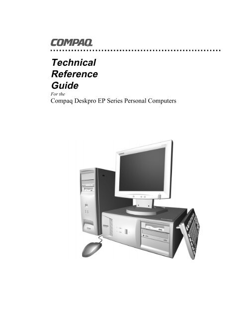
Compaq Deskpro EP Series Personal Computers
This hardcopy is designed to be placed into a standard 3-ring binder. Provided below is a title block that<br />
can be cut out and placed into the slip or taped onto the edge of the binder.<br />
Deskpro EP Series Personal Computers TRG
NOTICE<br />
The information in this document is subject to change without notice.<br />
<strong>Technical</strong> <strong>Reference</strong> <strong>Guide</strong><br />
COMPAQ COMPUTER CORPORATION SHALL NOT BE LIABLE FOR TECHNICAL OR<br />
EDITORIAL ERRORS OR OMISSIONS HEREIN; NOR FOR INCIDENTAL OR<br />
CONSEQUENTIAL DAMAGES RESULTING FROM THE FURNISHING, PERFORMANCE,<br />
OR USE OF THIS MATERIAL. IT IS THE RESPONSIBILITY OF MANUFACTURERS TO<br />
ENSURE THAT DEVICES DESIGNED TO BE USED WITH COMPAQ PRODUCTS<br />
COMPLY WITH FCC CLASS B EMISSIONS REQUIREMENTS.<br />
This guide contains information protected by copyright. No part of this document may be<br />
photocopied or reproduced in any form without prior written consent from Compaq Computer<br />
Corporation.<br />
©1998 Compaq Computer Corporation<br />
All rights reserved. Printed in the USA<br />
Compaq, Deskpro, LTE, Contura, Presario, ProLinea<br />
Registered U.S. Patent and Trademark Office<br />
Product names mentioned in this document may be trademarks and/or registered trademarks of other companies.<br />
“Pentium” and “MMX” are trademarks of Intel Corporation.<br />
“Windows” is a trademark of Microsoft Corporation.<br />
For more information regarding specifications and Compaq-specific parts please contact Compaq<br />
Computer Corporation, Industry Relations Department.<br />
<strong>Technical</strong> <strong>Reference</strong> <strong>Guide</strong><br />
for<br />
Compaq Deskpro EP Series Personal Computers<br />
First Edition - April 1998<br />
Document Number DSK-107A/0498<br />
Compaq Deskpro EP Series Personal Computers<br />
First Edition – April 1998<br />
i
<strong>Technical</strong> <strong>Reference</strong> <strong>Guide</strong><br />
ii<br />
Compaq Deskpro EP Series Personal Computers<br />
First Edition - April 1998
TABLE OF CONTENTS<br />
<strong>Technical</strong> <strong>Reference</strong> <strong>Guide</strong><br />
CHAPTER 1 INTRODUCTION.............................................................................................................<br />
1.1 ABOUT THIS GUIDE ........................................................................................................... 1-1<br />
1.1.1 USING THIS GUIDE ..................................................................................................... 1-1<br />
1.1.2 ADDITIONAL INFORMATION SOURCES.................................................................. 1-1<br />
1.2 NOTATIONAL CONVENTIONS.......................................................................................... 1-2<br />
1.2.1 VALUES........................................................................................................................ 1-2<br />
1.2.2 RANGES........................................................................................................................ 1-2<br />
1.2.3 SIGNAL LABELS.......................................................................................................... 1-2<br />
1.2.4 REGISTER NOTATION AND USAGE ......................................................................... 1-2<br />
1.2.5 BIT NOTATION............................................................................................................ 1-2<br />
1.3 COMMON ACRONYMS AND ABBREVIATIONS.............................................................. 1-3<br />
CHAPTER 2 SYSTEM OVERVIEW.....................................................................................................<br />
2.1 INTRODUCTION.................................................................................................................. 2-1<br />
2.2 FEATURES ........................................................................................................................... 2-2<br />
2.2.1 STANDARD FEATURES .............................................................................................. 2-2<br />
2.2.2 OPTIONS....................................................................................................................... 2-2<br />
2.3 MECHANICAL DESIGN ...................................................................................................... 2-3<br />
2.3.1 CABINET LAYOUT...................................................................................................... 2-3<br />
2.3.2 CHASSIS LAYOUT....................................................................................................... 2-4<br />
2.3.3 SYSTEM BOARD LAYOUT ......................................................................................... 2-5<br />
2.4 SYSTEM ARCHITECTURE.................................................................................................. 2-6<br />
2.4.1 PROCESSOR ................................................................................................................. 2-8<br />
2.4.2 MEMORY...................................................................................................................... 2-8<br />
2.4.3 SUPPORT CHIPSET...................................................................................................... 2-9<br />
2.4.4 MASS STORAGE .......................................................................................................... 2-9<br />
2.4.5 SERIAL AND PARALLEL INTERFACES .................................................................... 2-9<br />
2.4.6 UNIVERSAL SERIAL BUS INTERFACE ................................................................... 2-10<br />
2.4.7 GRAPHICS SUBSYSTEM........................................................................................... 2-10<br />
2.5 SPECIFICATIONS.............................................................................................................. 2-11<br />
CHAPTER 3 PROCESSOR/MEMORY SUBSYSTEM ........................................................................<br />
3.1 INTRODUCTION.................................................................................................................. 3-1<br />
3.2 66-MHZ SLOT 1 PROCESSOR/MEMORY SUBSYSTEM ................................................... 3-2<br />
3.2.1 CELERON PROCESSOR............................................................................................... 3-3<br />
3.2.2 PENTIUM II PROCESSOR............................................................................................ 3-3<br />
3.2.3 PROCESSOR CHANGING/UPGRADING..................................................................... 3-4<br />
3.2.4 SYSTEM MEMORY...................................................................................................... 3-5<br />
3.2.5 SUBSYSTEM CONFIGURATION................................................................................. 3-8<br />
3.3 100-MHZ SLOT 1 PROCESSOR/MEMORY SUBSYSTEM.................................................. 3-9<br />
Compaq Deskpro EP Series Personal Computers<br />
First Edition – April 1998<br />
iii
<strong>Technical</strong> <strong>Reference</strong> <strong>Guide</strong><br />
iv<br />
3.3.1 PENTIUM II PROCESSOR.......................................................................................... 3-10<br />
3.3.2 SYSTEM MEMORY.................................................................................................... 3-12<br />
3.3.3 SUBSYSTEM CONFIGURATION............................................................................... 3-13<br />
CHAPTER 4 SYSTEM SUPPORT.........................................................................................................<br />
4.1 INTRODUCTION.................................................................................................................. 4-1<br />
4.2 PCI BUS OVERVIEW........................................................................................................... 4-2<br />
4.2.1 PCI CONNECTOR......................................................................................................... 4-3<br />
4.2.2 PCI BUS MASTER ARBITRATION.............................................................................. 4-4<br />
4.2.3 PCI BUS TRANSACTIONS........................................................................................... 4-5<br />
4.2.4 OPTION ROM MAPPING ............................................................................................. 4-8<br />
4.2.5 PCI INTERRUPT MAPPING ......................................................................................... 4-9<br />
4.2.6 PCI POWER MANAGEMENT SUPPORT..................................................................... 4-9<br />
4.2.7 PCI CONFIGURATION............................................................................................... 4-10<br />
4.3 AGP BUS OVERVIEW ....................................................................................................... 4-11<br />
4.3.1 BUS TRANSACTIONS................................................................................................ 4-11<br />
4.3.2 AGP CONFIGURATION ............................................................................................. 4-14<br />
4.3.3 AGP CONNECTOR..................................................................................................... 4-15<br />
4.4 ISA BUS OVERVIEW......................................................................................................... 4-16<br />
4.4.1 ISA CONNECTOR ...................................................................................................... 4-17<br />
4.4.2 ISA BUS TRANSACTIONS......................................................................................... 4-18<br />
4.4.3 DIRECT MEMORY ACCESS...................................................................................... 4-20<br />
4.4.4 INTERRUPTS.............................................................................................................. 4-23<br />
4.4.5 INTERVAL TIMER..................................................................................................... 4-27<br />
4.4.6 ISA CONFIGURATION............................................................................................... 4-27<br />
4.5 SYSTEM CLOCK DISTRIBUTION.................................................................................... 4-28<br />
4.6 REAL-TIME CLOCK AND CONFIGURATION MEMORY............................................... 4-29<br />
4.6.1 CONFIGURATION MEMORY BYTE DEFINITIONS ................................................ 4-30<br />
4.7 I/O MAP AND REGISTER ACCESSING............................................................................ 4-46<br />
4.7.1 SYSTEM I/O MAP ...................................................................................................... 4-46<br />
4.7.2 82371 SOUTH BRIDGE GPIO CONFIGURATION..................................................... 4-47<br />
4.7.3 87309 I/O CONTROLLER CONFIGURATION ........................................................... 4-49<br />
4.8 SYSTEM MANAGEMENT SUPPORT ............................................................................... 4-50<br />
4.8.1 FLASH ROM WRITE PROTECT ................................................................................ 4-50<br />
4.8.2 USER SECURITY........................................................................................................ 4-50<br />
4.8.3 I/O SECURITY ............................................................................................................ 4-51<br />
4.8.4 POWER MANAGEMENT ........................................................................................... 4-51<br />
CHAPTER 5 INPUT/OUTPUT INTERFACES.....................................................................................<br />
5.1 INTRODUCTION.................................................................................................................. 5-1<br />
5.2 ENHANCED IDE INTERFACE ............................................................................................ 5-1<br />
5.2.1 IDE PROGRAMMING................................................................................................... 5-1<br />
5.2.2 IDE CONNECTOR ........................................................................................................ 5-9<br />
5.3 DISKETTE DRIVE INTERFACE........................................................................................ 5-10<br />
5.3.1 DISKETTE DRIVE PROGRAMMING ........................................................................ 5-11<br />
5.3.2 DISKETTE DRIVE CONNECTOR.............................................................................. 5-14<br />
5.4 SERIAL INTERFACE ......................................................................................................... 5-15<br />
Compaq Deskpro EP Series Personal Computers<br />
First Edition - April 1998
<strong>Technical</strong> <strong>Reference</strong> <strong>Guide</strong><br />
5.4.1 RS-232 INTERFACE ................................................................................................... 5-15<br />
5.4.2 SERIAL INTERFACE PROGRAMMING.................................................................... 5-16<br />
5.5 PARALLEL INTERFACE ................................................................................................... 5-21<br />
5.5.1 STANDARD PARALLEL PORT MODE ..................................................................... 5-21<br />
5.5.2 ENHANCED PARALLEL PORT MODE..................................................................... 5-22<br />
5.5.3 EXTENDED CAPABILITIES PORT MODE ............................................................... 5-22<br />
5.5.4 PARALLEL INTERFACE PROGRAMMING.............................................................. 5-23<br />
5.5.5 PARALLEL INTERFACE CONNECTOR ................................................................... 5-27<br />
5.6 KEYBOARD/POINTING DEVICE INTERFACE ............................................................... 5-28<br />
5.6.1 KEYBOARD INTERFACE OPERATION ................................................................... 5-28<br />
5.6.2 POINTING DEVICE INTERFACE OPERATION ....................................................... 5-30<br />
5.6.3 KEYBOARD/POINTING DEVICE INTERFACE PROGRAMMING ......................... 5-30<br />
5.6.4 KEYBOARD/POINTING DFEVICE INTERFACE CONNECTOR.............................. 5-34<br />
5.7 UNIVERSAL SERIAL BUS INTERFACE........................................................................... 5-35<br />
5.7.1 USB KEYBOARD CONSIDERATIONS...................................................................... 5-35<br />
5.7.2 USB CONFIGURATION.............................................................................................. 5-35<br />
5.7.3 USB CONTROL........................................................................................................... 5-36<br />
5.7.4 USB CONNECTOR ..................................................................................................... 5-36<br />
CHAPTER 6 POWER AND SIGNAL DISTRIBUTION.......................................................................<br />
6.1 INTRODUCTION.................................................................................................................. 6-1<br />
6.2 POWER SUPPLY ASSEMBLY/CONTROL .......................................................................... 6-1<br />
6.2.1 POWER SUPPLY ASSEMBLY...................................................................................... 6-2<br />
6.2.2 POWER CONTROL....................................................................................................... 6-3<br />
6.3 POWER DISTRIBUTION...................................................................................................... 6-5<br />
6.3.1 3/5/12 VDC DISTRIBUTION......................................................................................... 6-5<br />
6.3.2 LOW VOLTAGE DISTRIBUTION................................................................................ 6-6<br />
6.4 GENERAL SIGNAL DISTRIBUTION .................................................................................. 6-7<br />
CHAPTER 7 BIOS ROM .......................................................................................................................<br />
7.1 INTRODUCTION.................................................................................................................. 7-1<br />
7.2 BOOT FUNCTIONS.............................................................................................................. 7-2<br />
7.2.1 BOOT BLOCK............................................................................................................... 7-2<br />
7.2.2 QUICKBOOT................................................................................................................. 7-2<br />
7.2.3 SILENTBOOT ............................................................................................................... 7-2<br />
7.3 MEMORY DETECTION AND CONFIGURATION.............................................................. 7-3<br />
7.4 CLIENT MANAGEMENT SUPPORT................................................................................... 7-4<br />
7.4.1 SYSTEM ID/REVISION/SERIAL NO. .......................................................................... 7-6<br />
7.4.2 SYSTEM INFORMATION TABLE ............................................................................... 7-6<br />
7.4.3 EDID RETRIEVE ........................................................................................................ 7-12<br />
7.4.4 DRIVE FAULT PREDICTION..................................................................................... 7-12<br />
7.4.5 SYSTEM MAP RETRIEVAL....................................................................................... 7-13<br />
7.4.6 FLASH ROM FUNCTIONS ......................................................................................... 7-14<br />
7.4.7 POWER BUTTON FUNCTIONS................................................................................. 7-14<br />
7.4.8 ACCESSING CMOS.................................................................................................... 7-16<br />
Compaq Deskpro EP Series Personal Computers<br />
First Edition – April 1998<br />
v
<strong>Technical</strong> <strong>Reference</strong> <strong>Guide</strong><br />
vi<br />
7.4.9 ACCESSING CMOS FEATURE BITS......................................................................... 7-16<br />
7.4.10 SECURITY FUNCTIONS............................................................................................ 7-18<br />
7.5 PNP SUPPORT.................................................................................................................... 7-19<br />
7.5.1 SMBIOS....................................................................................................................... 7-20<br />
7.6 POWER MANAGEMENT FUNCTIONS ............................................................................ 7-21<br />
7.6.1 INDEPENDENT PM SUPPORT .................................................................................. 7-21<br />
7.6.2 ACPI SUPPORT........................................................................................................... 7-21<br />
7.6.3 APM SUPPORT ........................................................................................................... 7-22<br />
7.7 USB LEGACY SUPPORT ................................................................................................... 7-24<br />
7.8 BIOS UPGRADING............................................................................................................. 7-24<br />
APPENDIX A ERROR MESSAGES AND CODES...............................................................................<br />
A.1 INTRODUCTION.................................................................................................................A-1<br />
A.2 POWER-ON MESSAGES..................................................................................................... A-1<br />
A.3 BEEP/KEYBOARD LED CODES ........................................................................................ A-1<br />
A.4 POWER-ON SELF TEST (POST) MESSAGES.................................................................... A-2<br />
A.5 PROCESSOR ERROR MESSAGES (1XX-XX) ...................................................................... A-3<br />
A.6 MEMORY ERROR MESSAGES (2XX-XX)........................................................................... A-4<br />
A.7 KEYBOARD ERROR MESSAGES (30X-XX) ....................................................................... A-4<br />
A.8 PRINTER ERROR MESSAGES (4XX-XX) ............................................................................ A-5<br />
A.9 VIDEO (GRAPHICS) ERROR MESSAGES (5XX-XX).......................................................... A-5<br />
A.10 DISKETTE DRIVE ERROR MESSAGES (6XX-XX) ......................................................... A-6<br />
A.11 SERIAL INTERFACE ERROR MESSAGES (11XX-XX) ................................................... A-6<br />
A.12 MODEM COMMUNICATIONS ERROR MESSAGES (12XX-XX).................................... A-7<br />
A.13 HARD DRIVE ERROR MESSAGES (17XX-XX) ............................................................... A-8<br />
A.14 HARD DRIVE ERROR MESSAGES (19XX-XX) ............................................................... A-9<br />
A.15 VIDEO (GRAPHICS) ERROR MESSAGES (24XX-XX) .................................................... A-9<br />
A.16 AUDIO ERROR MESSAGES (3206-XX)......................................................................... A-10<br />
A.17 NETWORK INTERFACE ERROR MESSAGES (60XX-XX) ........................................... A-10<br />
A.18 SCSI INTERFACE ERROR MESSAGES (65XX-XX, 66XX-XX, 67XX-XX) ....................... A-11<br />
A.19 POINTING DEVICE INTERFACE ERROR MESSAGES (8601-XX).............................. A-11<br />
A.20 CEMM PRIVILEDGED OPS ERROR MESSAGES........................................................ A-12<br />
A.21 CEMM EXCEPTION ERROR MESSAGES ................................................................... A-12<br />
APPENDIX B ASCII CHARACTER SET .............................................................................................<br />
B.1 INTRODUCTION..................................................................................................................B-1<br />
APPENDIX C KEYBOARD ...................................................................................................................<br />
C.1 INTRODUCTION..................................................................................................................C-1<br />
C.2 KEYSTROKE PROCESSING................................................................................................C-2<br />
C.2.1 TRANSMISSIONS TO THE SYSTEM ..........................................................................C-3<br />
C.2.2 KEYBOARD LAYOUTS ...............................................................................................C-4<br />
C.2.3 KEYS.............................................................................................................................C-7<br />
C.2.4 KEYBOARD COMMANDS.........................................................................................C-10<br />
Compaq Deskpro EP Series Personal Computers<br />
First Edition - April 1998
<strong>Technical</strong> <strong>Reference</strong> <strong>Guide</strong><br />
C.2.5 SCAN CODES .............................................................................................................C-10<br />
APPENDIX D AUDIO CARD.................................................................................................................<br />
D.1 INTRODUCTION.................................................................................................................D-1<br />
D.2 FUNCTIONAL DESCRIPTION............................................................................................ D-2<br />
D.2.1 PCM AUDIO PROCESSING......................................................................................... D-4<br />
D.2.2 FM SYNTHESIS AUDIO PROCESSING...................................................................... D-7<br />
D.3 AUDIO CARD PROGRAMMING ........................................................................................ D-8<br />
D.3.1 CONFIGURATION....................................................................................................... D-8<br />
D.3.2 CONTROL....................................................................................................................D-9<br />
D.4 SPECIFICATIONS............................................................................................................. D-11<br />
APPENDIX E ATI RAGE IIC GRAPHICS CARD ...............................................................................<br />
E.1 INTRODUCTION..................................................................................................................E-1<br />
E.2 FUNCTIONAL DESCRIPTION.............................................................................................E-2<br />
E.2.1 ATI RAGE IIC GRAPHICS CONTROLLER..................................................................E-3<br />
E.3 DISPLAY CONFIGURATIONS ............................................................................................E-4<br />
E.4 PROGRAMMING..................................................................................................................E-5<br />
E.4.1 CONFIGURATION........................................................................................................E-5<br />
E.4.2 CONTROL.....................................................................................................................E-5<br />
E.5 POWER MANAGEMENT.....................................................................................................E-6<br />
E.5.1 MONITOR CONTROL ..................................................................................................E-6<br />
E.5.2 POWER CONSUMPTION .............................................................................................E-6<br />
E.6 CONNECTORS.....................................................................................................................E-7<br />
E.6.2 MONITOR CONNECTOR.............................................................................................E-7<br />
E.6.3 MULTIMEDIA INTERFACE CONNECTOR ................................................................E-8<br />
APPENDIX F ATI RAGE PRO AGP 1X GRAPHICS CARD ..............................................................<br />
F.1 INTRODUCTION..................................................................................................................F-1<br />
F.2 FUNCTIONAL DESCRIPTION.............................................................................................F-2<br />
F.2.1 ATI RAGE PRO TURBO AGP GRAPHICS CONTROLLER .........................................F-3<br />
F.3 DISPLAY MODES ................................................................................................................F-4<br />
F.4 PROGRAMMING..................................................................................................................F-5<br />
F.4.1 CONFIGURATION........................................................................................................F-5<br />
F.4.2 CONTROL.....................................................................................................................F-5<br />
F.5 MONITOR POWER MANAGEMENT CONTROL ...............................................................F-6<br />
F.6 CONNECTORS.....................................................................................................................F-6<br />
F.6.1 MEMORY EXPANSION CONNECTOR.......................................................................F-6<br />
F.6.2 MONITOR CONNECTOR.............................................................................................F-7<br />
F.6.3 MULTIMEDIA INTERFACE CONNECTOR ................................................................F-8<br />
Compaq Deskpro EP Series Personal Computers<br />
First Edition – April 1998<br />
vii
<strong>Technical</strong> <strong>Reference</strong> <strong>Guide</strong><br />
APPENDIX G DIAMOND FIRE GRAPHICS CARD ...........................................................................<br />
viii<br />
G.1 INTRODUCTION.................................................................................................................G-1<br />
G.2 FUNCTIONAL DESCRIPTION............................................................................................ G-2<br />
G.2.1 SGS nVIDIA RIVA 128 GRAPHICS CONTROLLER................................................... G-3<br />
G.3 DISPLAY MODES ............................................................................................................... G-4<br />
G.4 PROGRAMMING................................................................................................................. G-5<br />
G.4.1 CONFIGURATION....................................................................................................... G-5<br />
G.4.2 CONTROL....................................................................................................................G-5<br />
G.5 MONITOR POWER MANAGEMENT CONTROL .............................................................. G-6<br />
G.6 CONNECTORS.................................................................................................................... G-6<br />
G.6.1 MONITOR CONNECTOR............................................................................................ G-7<br />
G.6.2 MEDIA PORT CONNECTOR ...................................................................................... G-8<br />
Compaq Deskpro EP Series Personal Computers<br />
First Edition - April 1998
LIST OF FIGURES<br />
<strong>Technical</strong> <strong>Reference</strong> <strong>Guide</strong><br />
FIGURE 2–1. COMPAQ DESKPRO EP PERSONAL COMPUTERS WITH MONITOR .......................................... 2-1<br />
FIGURE 2–2. CABINET LAYOUT, FRONT VIEW ....................................................................................... 2-3<br />
FIGURE 2–3. CABINET LAYOUT, REAR VIEW ......................................................................................... 2-3<br />
FIGURE 2–4. CHASSIS LAYOUT, TOP VIEW ............................................................................................ 2-4<br />
FIGURE 2–5. SYSTEM BOARD LAYOUT, COMPONENT SIDE ..................................................................... 2-5<br />
FIGURE 2–6. SYSTEM ARCHITECTURE, BLOCK DIAGRAM........................................................................ 2-7<br />
FIGURE 2–7. PROCESSOR ARCHITECTURAL COMPARISON DIAGRAM........................................................ 2-8<br />
FIGURE 3–1. 66-MHZ SLOT 1 PROCESSOR/MEMORY SUBSYSTEM ARCHITECTURE................................... 3-2<br />
FIGURE 3–2. CELERON PROCESSOR INTERNAL ARCHITECTURE............................................................... 3-3<br />
FIGURE 3–3. PENTIUM II PROCESSOR INTERNAL ARCHITECTURE............................................................. 3-3<br />
FIGURE 3–4. SYSTEM MEMORY MAP..................................................................................................... 3-7<br />
FIGURE 3–5. 100-MHZ SLOT 1 PROCESSOR/MEMORY SUBSYSTEM ARCHITECTURE................................. 3-9<br />
FIGURE 3–6. 350-/400-MHZ PENTIUM II PROCESSOR INTERNAL ARCHITECTURE .................................. 3-10<br />
FIGURE 4–1. PCI BUS DEVICES AND FUNCTIONS..................................................................................... 4-2<br />
FIGURE 4–2. PCI BUS CONNECTOR (32-BIT TYPE)................................................................................. 4-3<br />
FIGURE 4–3. TYPE 0 CONFIGURATION CYCLE........................................................................................ 4-6<br />
FIGURE 4–4. PCI CONFIGURATION SPACE MAP...................................................................................... 4-7<br />
FIGURE 4–5. AGP 1X DATA TRANSFER (PEAK TRANSFER RATE: 266 MB/S) ........................................ 4-12<br />
FIGURE 4–6. AGP 2X DATA TRANSFER (PEAK TRANSFER RATE: 532 MB/S) ........................................ 4-13<br />
FIGURE 4–7. AGP BUS CONNECTOR ................................................................................................... 4-15<br />
FIGURE 4–8. ISA BUS BLOCK DIAGRAM................................................................................................ 4-16<br />
FIGURE 4–9. ISA EXPANSION CONNECTOR.......................................................................................... 4-17<br />
FIGURE 4–10. MASKABLE INTERRUPT PROCESSING, BLOCK DIAGRAM.................................................. 4-23<br />
FIGURE 4–11. CONFIGURATION MEMORY MAP.................................................................................... 4-29<br />
FIGURE 5–1. 40-PIN IDE CONNECTOR. ................................................................................................. 5-9<br />
FIGURE 5–2. 34-PIN DISKETTE DRIVE CONNECTOR.............................................................................. 5-14<br />
FIGURE 5–3. SERIAL INTERFACE CONNECTOR (MALE DB-9 AS VIEWED FROM REAR OF CHASSIS) ........... 5-15<br />
FIGURE 5–4. PARALLEL INTERFACE CONNECTOR (FEMALE DB-25 AS VIEWED FROM REAR OF CHASSIS) .. 5-27<br />
FIGURE 5–5. 8042-TO-KEYBOARD TRANSMISSION OF CODE EDH, TIMING DIAGRAM............................ 5-28<br />
FIGURE 5–6. KEYBOARD OR POINTING DEVICE INTERFACE CONNECTOR............................................... 5-34<br />
FIGURE 5–7. UNIVERSAL SERIAL BUS CONNECTOR (ONE OF TWO AS VIEWED FROM REAR OF CHASSIS)..... 5-36<br />
FIGURE 6–1. POWER SUPPLY ASSEMBLY AND ASSOCIATED CIRCUITRY, BLOCK DIAGRAM....................... 6-1<br />
FIGURE 6–2. POWER CABLE DIAGRAM .................................................................................................. 6-5<br />
FIGURE 6–3. LOW VOLTAGE REGULATOR CIRCUITRY, BLOCK DIAGRAM ................................................. 6-6<br />
FIGURE 6–4. GENERAL SIGNAL DISTRIBUTION, FUNCTIONAL BLOCK DIAGRAM....................................... 6-7<br />
FIGURE 6–5. FRONT PANEL (BEZEL) CONTROL/INDICATOR CONNECTOR ................................................ 6-8<br />
FIGURE 6–6. WAKE-ON-LAN NIC CONNECTOR.................................................................................... 6-8<br />
FIGURE B–1. ASCII CHARACTER SET ...................................................................................................B-1<br />
Compaq Deskpro EP Series Personal Computers<br />
First Edition – April 1998<br />
ix
<strong>Technical</strong> <strong>Reference</strong> <strong>Guide</strong><br />
FIGURE C–1. KEYSTROKE PROCESSING ELEMENTS, BLOCK DIAGRAM ....................................................C-2<br />
FIGURE C–2. KEYBOARD-TO-SYSTEM TRANSMISSION OF CODE 58H, TIMING DIAGRAM..........................C-3<br />
FIGURE C–3. U.S. ENGLISH (101-KEY) KEYBOARD KEY POSITIONS.......................................................C-4<br />
FIGURE C–4. NATIONAL (102-KEY) KEYBOARD KEY POSITIONS............................................................C-4<br />
FIGURE C–5. U.S. ENGLISH WINDOWS (101W-KEY) KEYBOARD KEY POSITIONS ...................................C-5<br />
FIGURE C–6. NATIONAL WINDOWS (102W-KEY) KEYBOARD KEY POSITIONS ........................................C-5<br />
FIGURE C–7. U.S. ENGLISH WINDOWS (101WE-KEY) KEYBOARD KEY POSITIONS.................................C-6<br />
FIGURE C–8. NATIONAL WINDOWS (102WE-KEY) KEYBOARD KEY POSITIONS......................................C-6<br />
FIGURE C–9. SCANNER ELEMENTS, BLOCK DIAGRAM..........................................................................C-14<br />
FIGURE C–10. SCANNER OPERATION FLOW CHART ..............................................................................C-16<br />
FIGURE D–1. AUDIO CARD LAYOUT..................................................................................................... D-1<br />
FIGURE D–2. AUDIO CARD BLOCK DIAGRAM........................................................................................ D-3<br />
FIGURE D–3. ANALOG SIGNAL SAMPLING/QUANTIZING ........................................................................ D-4<br />
FIGURE D–4. DAC OPERATION ........................................................................................................... D-5<br />
FIGURE D–5. AUDIO CARD-TO-ISA BUS PCM AUDIO DATA FORMATS / BYTE ORDERING...................... D-6<br />
FIGURE D–6. FM SYNTHESIS PATCH.................................................................................................... D-7<br />
FIGURE D–7. AUDIO CAR-TO-ISA BUS FM AUDIO DATA FORMAT ........................................................ D-7<br />
FIGURE E–1. ATI RAGE IIC AGP GRAPHICS CARD LAYOUT (COMPAQ P/N 332836-001) ......................... 1<br />
FIGURE E–2. ATI RAGE IIC AGP GRAPHICS CARD BLOCK DIAGRAM ...................................................... 2<br />
FIGURE E–3. ATI 3D RAGE IIC GRAPHICS CONTROLLER INTERNAL ARCHITECTURE ............................... 3<br />
FIGURE E–4. VGA MONITOR CONNECTOR, (FEMALE DB-15, AS VIEWED FROM REAR)................................. 7<br />
FIGURE E–5. MULTIMEDIA INTERFACE CONNECTOR (40-PIN HEADER P1).................................................. 8<br />
FIGURE F–1. ATI RAGE PRO AGP GRAPHICS CARD LAYOUT (P/N 008061-XXX)....................................F-1<br />
FIGURE F–2. ATI RAGE PRO AGP GRAPHICS CARD BLOCK DIAGRAM .................................................F-2<br />
FIGURE F–3. ATI 3DRAGE PRO GRAPHICS CONTROLLER INTERNAL ARCHITECTURE...............................F-3<br />
FIGURE F–4. VGA MONITOR CONNECTOR, (FEMALE DB-15, AS VIEWED FROM REAR). .............................F-7<br />
FIGURE F–5. MULTIMEDIA INTERFACE CONNECTOR (40-PIN HEADER P1)...............................................F-8<br />
FIGURE G–1. DIAMOND FIRE AGP GRAPHICS CARD LAYOUT................................................................. G-1<br />
FIGURE G–2. DIAMOND FIRE AGP GRAPHICS CARD BLOCK DIAGRAM ................................................... G-2<br />
FIGURE G–3. SGS NVIDIA RIVA 128 GRAPHICS CONTROLLER INTERNAL ARCHITECTURE................... G-3<br />
FIGURE G–4. VGA MONITOR CONNECTOR, (FEMALE DB-15, AS VIEWED FROM REAR). ........................... G-7<br />
FIGURE G–5. MEDIA PORT CONNECTOR (26-PIN HEADER P1) ............................................................... G-8<br />
x<br />
Compaq Deskpro EP Series Personal Computers<br />
First Edition - April 1998
LIST OF TABLES<br />
<strong>Technical</strong> <strong>Reference</strong> <strong>Guide</strong><br />
TABLE 1–1. ACRONYMS AND ABBREVIATIONS....................................................................................... 1-3<br />
TABLE 2–1. ARCHITECTURAL COMPARISON............................................................................................. 2-6<br />
TABLE 2–2. SUPPORT CHIPSETS ............................................................................................................ 2-9<br />
TABLE 2–3. GRAPHICS SUBSYSTEM COMPARISON ................................................................................ 2-10<br />
TABLE 2–4. ENVIRONMENTAL SPECIFICATIONS.................................................................................... 2-11<br />
TABLE 2–5. ELECTRICAL SPECIFICATIONS ........................................................................................... 2-11<br />
TABLE 2–6. PHYSICAL SPECIFICATIONS............................................................................................... 2-11<br />
TABLE 2–7. DISKETTE DRIVE SPECIFICATIONS..................................................................................... 2-12<br />
TABLE 2–8. 8X CD-ROM DRIVE SPECIFICATIONS................................................................................ 2-12<br />
TABLE 2–9. HARD DRIVE SPECIFICATIONS........................................................................................... 2-13<br />
TABLE 3–1. PROCESSOR/MEMORY ARCHITECTURAL COMPARISON........................................................... 3-1<br />
TABLE 3–2. PENTIUM II COVINGTON PROCESSOR BUS/CORE SPEED SWITCH SETTINGS....................... 3-4<br />
TABLE 3–3. SPD ADDRESS MAP (SDRAM DIMM)................................................................................. 3-6<br />
TABLE 3–4. HOST/PCI BRIDGE CONFIGURATION REGISTERS (443EX, FUNCTION 0) ................................ 3-8<br />
TABLE 3–5. PENTIUM II MICROPROCESSOR BUS/CORE SPEED SWITCH SETTINGS .................................. 3-11<br />
TABLE 3–6. HOST/PCI BRIDGE CONFIGURATION REGISTERS (443BX, FUNCTION 0) .............................. 3-13<br />
TABLE 4–1. PCI BUS CONNECTOR PINOUT............................................................................................ 4-3<br />
TABLE 4–2. PCI BUS MASTERING DEVICES ........................................................................................... 4-4<br />
TABLE 4–3. PCI DEVICE CONFIGURATION ACCESS ................................................................................ 4-6<br />
TABLE 4–4. PCI FUNCTION CONFIGURATION ACCES.............................................................................. 4-7<br />
TABLE 4–5. PCI DEVICE IDENTIFICATION ............................................................................................. 4-8<br />
TABLE 4–6. PCI/ISA BRIDGE CONFIGURATION REGISTERS (82371, FUNCTION 0).................................. 4-10<br />
TABLE 4–7. PCI/AGP BRIDGE CONFIGURATION REGISTERS (82371, FUNCTION 1)................................. 4-14<br />
TABLE 4–8. AGP BUS CONNECTOR PINOUT ......................................................................................... 4-15<br />
TABLE 4–9. ISA EXPANSION CONNECTOR PINOUT............................................................................... 4-17<br />
TABLE 4–10. DEFAULT DMA CHANNEL ASSIGNMENTS ....................................................................... 4-20<br />
TABLE 4–11. DMA PAGE REGISTER ADDRESSES ................................................................................. 4-21<br />
TABLE 4–12. DMA CONTROLLER REGISTERS...................................................................................... 4-22<br />
TABLE 4–13. MASKABLE INTERRUPT PRIORITIES AND ASSIGNMENTS.................................................... 4-24<br />
TABLE 4–14. MASKABLE INTERRUPT CONTROL REGISTERS.................................................................. 4-24<br />
TABLE 4–15. INTERVAL TIMER FUNCTIONS ......................................................................................... 4-27<br />
TABLE 4–16. INTERVAL TIMER CONTROL REGISTERS........................................................................... 4-27<br />
TABLE 4–17. CLOCK GENERATION AND DISTRIBUTION ........................................................................ 4-28<br />
TABLE 4–18. CONFIGURATION MEMORY (CMOS) MAP....................................................................... 4-30<br />
TABLE 4–19. SYSTEM I/O MAP........................................................................................................... 4-46<br />
TABLE 4–20. 82371 SOUTH BRIDGE GENERAL PURPOSE INPUT PORT UTILIZATION ............................... 4-47<br />
TABLE 4–21. 82371 SOUTH BRIDGE GENERAL PURPOSE OUTPUT PORT UTILIZATION ............................ 4-48<br />
TABLE 4–22. 87309 I/O CONTROLLER PNP STANDARD CONFIGURATION REGISTERS.............................. 4-49<br />
TABLE 5–1. IDE PCI CONFIGURATION REGISTERS ................................................................................ 5-2<br />
Compaq Deskpro EP Series Personal Computers xi<br />
First Edition – April 1998
<strong>Technical</strong> <strong>Reference</strong> <strong>Guide</strong><br />
TABLE 5–2. IDE BUS MASTER CONTROL REGISTERS ............................................................................. 5-3<br />
TABLE 5–3. IDE ATA CONTROL REGISTERS......................................................................................... 5-4<br />
TABLE 5–4. IDE CONTROLLER COMMANDS .......................................................................................... 5-7<br />
TABLE 5–5. 40-PIN IDE CONNECTOR PINOUT ....................................................................................... 5-9<br />
TABLE 5–6. DISKETTE DRIVE CONTROLLER CONFIGURATION REGISTERS ............................................. 5-11<br />
TABLE 5–7. DISKETTE DRIVE CONTROLLER REGISTERS ....................................................................... 5-12<br />
TABLE 5–8. 34-PIN DISKETTE DRIVE CONNECTOR PINOUT................................................................... 5-14<br />
TABLE 5–9. DB-9 SERIAL CONNECTOR PINOUT................................................................................... 5-15<br />
TABLE 5–10. SERIAL INTERFACE CONFIGURATION REGISTERS.............................................................. 5-16<br />
TABLE 5–11. SERIAL INTERFACE CONTROL REGISTERS........................................................................ 5-17<br />
TABLE 5–12. PARALLEL INTERFACE CONFIGURATION REGISTERS......................................................... 5-23<br />
TABLE 5–13. PARALLEL INTERFACE CONTROL REGISTERS ................................................................... 5-24<br />
TABLE 5–14. DB-25 PARALLEL CONNECTOR PINOUT .......................................................................... 5-27<br />
TABLE 5–15. 8042-TO-KEYBOARD COMMANDS .................................................................................. 5-29<br />
TABLE 5–16. KEYBOARD/MOUSE INTERFACE CONFIGURATION REGISTERS ........................................... 5-30<br />
TABLE 5–17. CPU COMMANDS TO THE 8042...................................................................................... 5-32<br />
TABLE 5–18. KEYBOARD/POINTING DEVICE CONNECTOR PINOUT........................................................ 5-34<br />
TABLE 5–19. USB INTERFACE CONFIGURATION REGISTERS................................................................. 5-35<br />
TABLE 5–20. USB CONTROL REGISTERS............................................................................................. 5-36<br />
TABLE 5–21. USB CONNECTOR PINOUT .............................................................................................. 5-36<br />
TABLE 6–1. POWER SUPPLY ASSEMBLY SPECIFICATIONS........................................................................ 6-2<br />
TABLE 7–1. PNP CLIENT MANAGEMENT FUNCTIONS (INT15)................................................................ 7-4<br />
TABLE 7–2. PNP BIOS FUNCTIONS..................................................................................................... 7-19<br />
TABLE 7–3. APM BIOS FUNCTIONS (INT15) ..................................................................................... 7-23<br />
TABLE A–1. POWER-ON MESSAGES ..................................................................................................... A-1<br />
TABLE A–2. BEEP/KEYBOARD LED CODES.......................................................................................... A-1<br />
TABLE A–3. POWER-ON SELF TEST (POST) MESSAGES........................................................................ A-2<br />
TABLE A–4. PROCESSOR ERROR MESSAGES ......................................................................................... A-3<br />
TABLE A–5. MEMORY ERROR MESSAGES............................................................................................. A-4<br />
TABLE A–6. KEYBOARD ERROR MESSAGES.......................................................................................... A-4<br />
TABLE A–7. PRINTER ERROR MESSAGES.............................................................................................. A-5<br />
TABLE A–8. VIDEO (GRAPHICS) ERROR MESSAGES .............................................................................. A-5<br />
TABLE A–9. DISKETTE DRIVE ERROR MESSAGES.................................................................................. A-6<br />
TABLE A–10. SERIAL INTERFACE ERROR MESSAGES............................................................................. A-6<br />
TABLE A–11. SERIAL INTERFACE ERROR MESSAGES............................................................................. A-7<br />
TABLE A–12. HARD DRIVE ERROR MESSAGES...................................................................................... A-8<br />
TABLE A–13. HARD DRIVE ERROR MESSAGES...................................................................................... A-9<br />
TABLE A–14. HARD DRIVE MESSAGES................................................................................................. A-9<br />
TABLE A–15. AUDIO ERROR MESSAGES............................................................................................. A-10<br />
TABLE A–16. NETWORK INTERFACE ERROR MESSAGES...................................................................... A-10<br />
TABLE A–17. SCSI INTERFACE ERROR MESSAGES ............................................................................. A-11<br />
TABLE A–18. POINTING DEVICE INTERFACE ERROR MESSAGES........................................................... A-11<br />
TABLE A–19. CEMM PRIVILEGED OPS ERROR MESSAGES.................................................................. A-12<br />
TABLE A–20. CEMM EXCEPTION ERROR MESSAGES ......................................................................... A-12<br />
xii<br />
Compaq Deskpro EP Series Personal Computers<br />
First Edition - April 1998
<strong>Technical</strong> <strong>Reference</strong> <strong>Guide</strong><br />
TABLE C–1. KEYBOARD-TO-SYSTEM COMMANDS ...............................................................................C-10<br />
TABLE C–2. KEYBOARD SCAN CODES.................................................................................................C-11<br />
TABLE C–3. SCANNER PERFORMANCE CHART .....................................................................................C-17<br />
TABLE C–4. SCANNER I/F SIGNALS.....................................................................................................C-18<br />
TABLE C–5. SCANNER SPECIFICATIONS...............................................................................................C-20<br />
TABLE D–1. AUDIO MODE DIFFERENCES.............................................................................................. D-6<br />
TABLE D–2. AUDIO CARD I/O MAP ..................................................................................................... D-9<br />
TABLE D–3. COMPATIBILITY MODE AUDIO MIXER CONTROL REGISTER MAPPING ................................... D-9<br />
TABLE D–4. EXTENDED MODE AUDIO MIXER CONTROL REGISTER MAPPING ........................................ D-10<br />
TABLE D–5. FM SYNTHESIZER CONTROL REGISTER MAPPING .............................................................. D-10<br />
TABLE D–6. AUDIO CARD SPECIFICATIONS ........................................................................................ D-11<br />
TABLE E–1. 2D GRAPHICS DISPLAY MODES (W/EDO RAM) ...................................................................... 4<br />
TABLE E–2. 3D GRAPHICS DISPLAY MODES............................................................................................... 4<br />
TABLE E–3. ATI RAGE IIC PCI CONFIGURATION SPACE REGISTERS ....................................................... 5<br />
TABLE E–4. STANDARD VGA MODE I/O MAPPING .................................................................................. 5<br />
TABLE E–5. MONITOR POWER MANAGEMENT CONDITIONS ...................................................................... 6<br />
TABLE E–6. DB-15 MONITOR CONNECTOR PINOUT ................................................................................. 7<br />
TABLE E–7. MULTIMEDIA INTERFACE CONNECTOR PINOUT ...................................................................... 8<br />
TABLE F–1. 2D GRAPHICS DISPLAY MODES (W/SGRAM)........................................................................F-4<br />
TABLE F–2. 3D GRAPHICS DISPLAY MODES ............................................................................................F-4<br />
TABLE F–3. ATI RAGE PRO PCI CONFIGURATION SPACE REGISTERS ..................................................F-5<br />
TABLE F–4. STANDARD VGA MODE I/O MAPPING................................................................................F-5<br />
TABLE F–5. MONITOR POWER MANAGEMENT CONDITIONS....................................................................F-6<br />
TABLE F–6. DB-15 MONITOR CONNECTOR PINOUT...............................................................................F-7<br />
TABLE F–7. MULTIMEDIA INTERFACE CONNECTOR PINOUT ...................................................................F-8<br />
TABLE G–1. 2D GRAPHICS DISPLAY MODES (W/SGRAM)...................................................................... G-4<br />
TABLE G–2. SGS NVIDA RIVA 128 PCI CONFIGURATION SPACE REGISTERS...................................... G-5<br />
TABLE G–3. STANDARD VGA MODE I/O MAPPING .............................................................................. G-5<br />
TABLE G–4. MONITOR POWER MANAGEMENT CONDITIONS.................................................................. G-6<br />
TABLE G–5. DB-15 MONITOR CONNECTOR PINOUT ............................................................................. G-7<br />
TABLE G–6. MEDIA PORT CONNECTOR PINOUT.................................................................................... G-8<br />
Compaq Deskpro EP Series Personal Computers<br />
First Edition – April 1998<br />
xiii
<strong>Technical</strong> <strong>Reference</strong> <strong>Guide</strong><br />
xiv<br />
Compaq Deskpro EP Series Personal Computers<br />
First Edition - April 1998
Chapter 1<br />
INTRODUCTION<br />
1. Chapter 1 INTRODUCTION<br />
1.1 ABOUT THIS GUIDE<br />
<strong>Technical</strong> <strong>Reference</strong> <strong>Guide</strong><br />
This guide provides technical information about the Compaq Deskpro EP Series of Personal<br />
Computers. This document includes information regarding system design, function, and features<br />
that can be used by programmers, engineers, technicians, and system administrators.<br />
1.1.1 USING THIS GUIDE<br />
This guide consists of chapters and appendices. The chapters primarily describe the hardware<br />
and firmware elements contained within the chassis and specifically deal with the system board<br />
and the power supply assembly. The appendices contain general information about standard<br />
peripheral devices such as the keyboard as well as separate audio or other interface cards, as well<br />
as other general information in tabular format.<br />
1.1.2 ADDITIONAL INFORMATION SOURCES<br />
This guide does not describe in detail other manufacturer’s components used in the product<br />
covered. For more information on individual commercial-off-the-shelf (COTS) components refer<br />
to the indicated manufacturers’ documentation. The products covered by this guide use<br />
architecture based on industry-standard specifications that can be referenced for detailed<br />
information.<br />
Hardcopy documentation sources:<br />
♦ The Lotus/Intel/Microsoft Expanded Memory Specification, Ver. 4.0<br />
♦ PCI Local Bus Specification Revision 2.1<br />
Online information sources:<br />
♦ Compaq Computer Corporation: http://www.compaq.com<br />
♦ Intel Corporation: http://www.intel.com<br />
♦ National Semiconductor Incorporated: http://www.national.com<br />
♦ AGP forum: http://www.agpforum.org/index.htm<br />
♦ ATI Incorporated: http://www.atitech.com<br />
♦ NVIDIA Corp.: http://www.nvidia.com<br />
Compaq Deskpro EP Series of Personal Computers<br />
First Edition - April 1998<br />
1-1
Chapter 1 Introduction<br />
1.2 NOTATIONAL CONVENTIONS<br />
1.2.1 VALUES<br />
1-2<br />
Hexadecimal values are indicated by the letter “h” following an alpha-numerical value. Binary<br />
values are indicated by the letter “b” following a value of ones and zeros. Memory addresses<br />
expressed as “SSSS:OOOO” (SSSS = 16-bit segment, OOOO = 16-bit offset) can be assumed as<br />
a hexadecimal value. Values that have no succeeding letter can be assumed to be decimal.<br />
1.2.2 RANGES<br />
Ranges or limits for a parameter are shown as a pair of values separated by two dots:<br />
Example: Bits = bits 7, 6, 5, and 4.<br />
1.2.3 SIGNAL LABELS<br />
Signal names are indicated using abbreviations, acronyms, or, if possible, the full signal name in<br />
all capital letters. Signals that are meant to be active low are indicated with a dash immediately<br />
following the name.<br />
1.2.4 REGISTER NOTATION AND USAGE<br />
This guide uses standard Intel naming conventions in discussing the microprocessor’s (CPU)<br />
internal registers. Registers that are accessed through programmable I/O using an indexing<br />
scheme are indicated using the following format:<br />
03C5.17h<br />
Compaq Deskpro EP Series of Personal Computers<br />
Index port<br />
Data port<br />
In the example above, register 03C5.17h is accessed by writing the index port value 17h to the<br />
index address (03C4h), followed by a write to or a read from port 03C5h.<br />
1.2.5 BIT NOTATION<br />
Bit values are labeled with bit representing the least-significant bit (LSb) and bit <br />
representing the most-significant bit (MSb) of a byte. Bytes, words, double words, and quad<br />
words are typically shown with most-significant portions on the left or top and the leastsignificant<br />
portions on the right or bottom respectively.<br />
First Edition – April 1998
1.3 COMMON ACRONYMS AND ABBREVIATIONS<br />
Table 1-1 lists the acronyms and abbreviations used in this guide.<br />
Table 1–1. Acronyms and Abbreviations<br />
Table 1-1.<br />
Acronyms and Abbreviations<br />
Acronym/Abbreviation Description<br />
A ampere<br />
AC alternating current<br />
ACPI Advanced Configuration and Power Interface<br />
A/D analog-to-digital<br />
AGP Accelerated graphics port<br />
API application programming interface<br />
APM advanced power management<br />
ASIC application-specific integrated circuit<br />
AT 1. attention (commands) 2. 286-based PC architecture<br />
ATA AT attachment (mode)<br />
AVI audio-video interleaved<br />
AVGA Advanced VGA<br />
BCD binary-coded decimal<br />
BIOS basic input/output system<br />
bis second/new revision<br />
BitBLT bit block transfer<br />
BNC Bayonet Neill-Concelman (connector)<br />
bps or b/s bits per second<br />
BSP Bootstrap processor<br />
CAS column address strobe<br />
CD compact disk<br />
CD-ROM compact disk read-only memory<br />
CDS compct disk system<br />
CF carry flag<br />
CGA color graphics adapter<br />
Ch channel<br />
CLUT color look-up table (pallete)<br />
cm centimeter<br />
CMC cache/memory controller<br />
CMOS complimentary metal-oxide semiconductor (configuration memory)<br />
Cntlr controller<br />
codec compressor/decompressor<br />
CPQ Compaq<br />
CPU central processing unit<br />
CRT cathode ray tube<br />
CSM Compaq system management / Compaq server management<br />
DAA direct access arrangement<br />
DAC digital-to-analog converter<br />
db decibel<br />
DC direct current<br />
DCH DOS compatibility hole<br />
DDC Display Data Channel<br />
DF direction flag<br />
<strong>Technical</strong> <strong>Reference</strong> <strong>Guide</strong><br />
Compaq Deskpro EP Series of Personal Computers<br />
First Edition - April 1998<br />
Continued<br />
1-3
Chapter 1 Introduction<br />
1-4<br />
Table 1-1. Acronyms and Abbreviations Continued<br />
Acronym/Abbreviation Description<br />
DIMM dual inline memory module<br />
DIN Deutche IndustriNorm (connector standard)<br />
DIP dual inline package<br />
DMA direct memory access<br />
DMI Desktop management interface<br />
dpi dots per inch<br />
DRAM dynamic random access memory<br />
DRQ data request<br />
ECC error correction coding<br />
EDID extended display identification data<br />
EDO extended data out (RAM type)<br />
EEPROM electrically eraseable PROM<br />
EGA enhanced graphics adapter<br />
EIA Electronic Industry Association<br />
EISA extended ISA<br />
EPP enhanced parallel port<br />
EIDE enhanced IDE<br />
ESCD Extended System Configuration Data (format)<br />
EV Environmental Variable (data)<br />
ExCA Exchangeable Card Architecture<br />
FIFO first in / first out<br />
FL flag (register)<br />
FM frequency modulation<br />
FPM fast page mode (RAM type)<br />
FPU Floating point unit (numeric or math coprocessor)<br />
ft foot<br />
GB gigabyte<br />
GND ground<br />
GPIO general purpose I/O<br />
GPOC general purpose open-collector<br />
GUI graphics user interface<br />
h hexadecimal<br />
HW hardware<br />
hex hexadecimal<br />
Hz hertz<br />
IDE integrated drive element<br />
IEEE Institute of Electrical and Electronic Engineers<br />
IF interrupt flag<br />
I/F interface<br />
in inch<br />
INT interrupt<br />
I/O input/output<br />
IPL initial program loader<br />
IrDA InfraRed Data Association<br />
IRQ interrupt request<br />
ISA industry standard architecture<br />
JEDEC Joint Electron Device Engineering Council<br />
Kb / KB kilobits / kilobytes (x 1024 bits / x 1024 bytes)<br />
Kb/s kilobits per second<br />
kg kilogram<br />
KHz kilohertz<br />
kv kilovolt<br />
Compaq Deskpro EP Series of Personal Computers<br />
First Edition – April 1998<br />
Continued
Table 1-1. Acronyms and Abbreviations Continued<br />
Acronym/Abbreviation Description<br />
lb pound<br />
LCD liquid crystal display<br />
LED light-emitting diode<br />
LIF low insertion force (socket)<br />
LSI large scale integration<br />
LSb / LSB least significant bit / least significant byte<br />
LUN logical unit (SCSI)<br />
MMX multimedia extensions<br />
MPEG Motion Picture Experts Group<br />
ms millisecond<br />
MSb / MSB most significant bit / most significant byte<br />
mux multiplex<br />
MVA motion video acceleration<br />
MVW motion video window<br />
n variable parameter/value<br />
NIC network interface card/controller<br />
NiCad nickel cadmium<br />
NiMH nickel-metal hydride<br />
NMI non-maskable interrupt<br />
ns nanosecond<br />
NT nested task flag<br />
NTSC National Television Standards Committee<br />
NVRAM non-volatile random access memory<br />
OEM original equipment manufacturer<br />
OS operating system<br />
PAL 1. programmable array logic 2. phase altering line<br />
PC personal computer<br />
PCI peripheral component interconnect<br />
PCM pulse code modulation<br />
PCMCIA Personal Computer Memory Card International Association<br />
PF parity flag<br />
PIN personal identification number<br />
PIO Programmed I/O<br />
POST power-on self test<br />
PROM programmable read-only memory<br />
PTR pointer<br />
RAM random access memory<br />
RAS row address strobe<br />
rcvr receiver<br />
RF resume flag<br />
RGB red/green/blue (monitor input)<br />
RH Relative humidity<br />
RMS root mean square<br />
ROM read-only memory<br />
RPM revolutions per minute<br />
RTC real time clock<br />
R/W read/write<br />
<strong>Technical</strong> <strong>Reference</strong> <strong>Guide</strong><br />
Compaq Deskpro EP Series of Personal Computers<br />
First Edition - April 1998<br />
Continued<br />
1-5
Chapter 1 Introduction<br />
1-6<br />
Table 1-1. Acronyms and Abbreviations Continued<br />
Acronym/Abbreviation Description<br />
SCSI small computer system interface<br />
SDRAM Synchronous Dynamic RAM<br />
SEC Single Edge-Connector<br />
SECAM sequential colour avec memoire (sequential color with memory)<br />
SF sign flag<br />
SGRAM Synchronous Graphics RAM<br />
SIMM single in-line memory module<br />
SIT system information table<br />
SMART Self Monitor Analysis Report Technology<br />
SMI system management interrupt<br />
SMM system management mode<br />
SMRAM system management RAM<br />
SPD serial presence detect<br />
SPP standard parallel port<br />
SRAM static RAM<br />
STN super twist pneumatic<br />
SVGA super VGA<br />
SW software<br />
TAD telephone answering device<br />
TAM telephone answering machine<br />
TCP tape carrier package<br />
TF trap flag<br />
TFT thin-film transistor<br />
TIA Telecommunications Information Administration<br />
TPE twisted pair ethernet<br />
TPI track per inch<br />
TTl transistor-transistor logic<br />
TV television<br />
TX transmit<br />
UART universal asynchronous receiver/transmitter<br />
UDMA Ultra DMA<br />
us / μs microsecond<br />
USB Universal Serial Bus<br />
UTP unshielded twisted pair<br />
V volt<br />
VESA Video Electronic Standards Association<br />
VGA video graphics adapter<br />
vib vibrato<br />
VLSI very large scale integration<br />
VRAM Video RAM<br />
W watt<br />
WRAM Windows RAM<br />
ZF zero flag<br />
ZIF zero insertion force (socket)<br />
Compaq Deskpro EP Series of Personal Computers<br />
First Edition – April 1998
Chapter 2<br />
SYSTEM OVERVIEW<br />
2. Chapter 2 SYSTEM OVERVIEW<br />
2.1 INTRODUCTION<br />
<strong>Technical</strong> <strong>Reference</strong> <strong>Guide</strong><br />
This chapter describes Compaq Deskpro EP Series of Personal Computers (Figure 2-1) based on<br />
the Pentium II Series of processors. The architecture employed by these systems incorporates the<br />
PCI, AGP, and ISA buses. All models are easily upgradeable and expandable to keep pace with<br />
business needs.<br />
Figure 2–1. Compaq Deskpro EP Personal Computers with Monitor<br />
Compaq Deskpro EP Series of Personal Computers<br />
First Edition–- April1998<br />
2-1
Chapter 2 System Overview<br />
2.2 FEATURES<br />
2-2<br />
This section describes the standard and distinguishing features.<br />
2.2.1 STANDARD FEATURES<br />
The following standard features are included on all models:<br />
♦ Celeron or Pentium II processor<br />
♦ 3.5 inch, 1.44-MB diskette drive<br />
♦ Extended IDE controller support for up to four IDE drives<br />
♦ Hard drive fault prediction (SMART-compatible)<br />
♦ Two serial interfaces<br />
♦ Parallel interface<br />
♦ Two universal serial bus ports<br />
♦ Two or Three PCI slots (depending on model)<br />
♦ Two or three ISA slots (depending on model)<br />
♦ One combo ISA/PCI slot<br />
♦ Compaq Space Saver keyboard w/Windows support<br />
♦ Compaq PS/2-type mouse<br />
♦ Power management support (APM 1.2 and ACPI)<br />
♦ Plug ’n Play compatible (with ESCD support)<br />
♦ Intelligent Manageability features including:<br />
• Asset management<br />
• Fault management<br />
• Security management<br />
• Configuration management<br />
• Integration management<br />
2.2.2 OPTIONS<br />
Options that are specific to the Compaq Deskpro EP Series of Personal Computers include:<br />
♦ System Memory: 16-MB DIMM<br />
32-MB DIMM<br />
64-MB DIMM<br />
128-MB DIMM<br />
Compaq Deskpro Computers are easily upgraded and enhanced with peripheral devices designed<br />
to meet PCI and ISA standards. The Compaq Deskpro Personal Computers are compatible with<br />
peripherals design for Plug ’n Play operation.<br />
Compaq Deskpro EP Series of Personal Computers<br />
First Edition – April 1998
2.3 MECHANICAL DESIGN<br />
2.3.1 CABINET LAYOUT<br />
1<br />
2<br />
Item Function<br />
1 Power On Light<br />
2 Hard Drive Activity Light<br />
3 Power Button<br />
4 Internal Drive (3.5” drive bay)<br />
5 Internal Drive (3.5” drive bay)<br />
6 1.44 MB Diskette Drive (5.25” drive bay)<br />
7 CD-ROM Drive (CDS models) (5.25“ drive bay)<br />
8 Internal Drive 5.25” drive bay)<br />
NOTES: [1] All units may be configured as either a desktop or a minitower.<br />
Figure 2–2. Cabinet Layout, Front View<br />
4<br />
3 5 6 7<br />
1 2 3 5 6 7 8 10<br />
Figure 2–3. Cabinet Layout, Rear View<br />
4<br />
9<br />
8<br />
Desktop Configuration Minitower Configuration [1]<br />
<strong>Technical</strong> <strong>Reference</strong> <strong>Guide</strong><br />
Compaq Deskpro EP Series of Personal Computers<br />
First Edition–- April1998<br />
Item Function<br />
1 AC Line In Connector<br />
2 Line Voltage Select Switch<br />
3 Universal serial bus interface (port A)<br />
4 Universal serial bus interface (port B)<br />
5 Keyboard connector<br />
6 Mouse connector<br />
7 Parallel interface<br />
8 Serial interface A (COM1)<br />
9 Serial interface B (COM2)<br />
10 Video graphics connector<br />
2-3
Chapter 2 System Overview<br />
2.3.2 CHASSIS LAYOUT<br />
2-4<br />
NOTE:<br />
Audio Board<br />
(in ISA slot) [1]<br />
ATX Graphics<br />
Board<br />
(in AGP slot)<br />
[1] Audio board present only on CDS models.<br />
[2] Chassis fan only present on models using 66-MHz slot 1 (2-DIMM) system board.<br />
[3] 100-MHz slot 1 system board shown.<br />
Figure 2–4. Chassis Layout, Top View<br />
Compaq Deskpro EP Series of Personal Computers<br />
Back<br />
First Edition – April 1998<br />
Front<br />
Chassis Fan [2]<br />
Power Supply<br />
System Board [3]<br />
Drive Bays<br />
(with drivelocks)
20<br />
19<br />
18<br />
17<br />
1 2<br />
2.3.3 SYSTEM BOARD LAYOUT<br />
3<br />
4 5 6 7 8 9<br />
66-MHz Slot 1 (2-DIMM) System Board<br />
(ATX-type, P/N 008312-xxx)<br />
Item Function Notes<br />
1 ISA expansion connectors [1]<br />
2 CMOS Battery<br />
3 PCI expansion connectors [2]<br />
4 AGP connector (J40)<br />
5 Serial connectors (J24): top, COM2; bottom, COM1<br />
6 Parallel interface connector (J9)<br />
7 Mouse connector (J8)<br />
8 Keyboard connector (J7)<br />
9 Universal serial ports (J6): top, port B; bottom, port A<br />
10 Microprocessor (in slot 1 connector)<br />
11 Chassis fan connector (P8)<br />
12 DIMM sockets (J1-J3, top to bottom) [3]<br />
13 Power supply connector (P1)<br />
14 Diskette drive connector (P10)<br />
15 IDE hard drive connector (secondary) (P21)<br />
16 IDE hard drive connector (primary) (P20)<br />
17 CMOS/password clear jumper (E50)<br />
18 Power LED/speaker/reset connector P5<br />
19 Frequency select DIP switch (SW1)<br />
20 Wake-on-LAN header P9<br />
NOTES:<br />
[1] On p/n 008312, J10-J12 left-to-right, J12 shares slot with PCI connector.<br />
On p/n 009635, J11-J10 left-to-right, J10 shares slot with PCI connector.<br />
[2] On p/n 008312, J22-J20 left-to-right, J22 shares slot with ISA connector.<br />
On p/n 009635, J23-J20 left-to-right, J23 shares slot with ISA connector.<br />
[3] Only two DIMM slots (J1, J2) on p/n 008312.<br />
Figure 2–5. System Board Layout, Component Side<br />
10<br />
11<br />
12<br />
13<br />
14<br />
15<br />
16<br />
20<br />
19<br />
18<br />
17<br />
<strong>Technical</strong> <strong>Reference</strong> <strong>Guide</strong><br />
Compaq Deskpro EP Series of Personal Computers<br />
First Edition–- April1998<br />
1 2<br />
3<br />
4 5 6 7 8 9<br />
100-MHz Slot 1 (3-DIMM) System Board<br />
(ATX-type, P/N 009635-xxx)<br />
2-5<br />
10<br />
11<br />
12<br />
13<br />
14<br />
15<br />
16
Chapter 2 System Overview<br />
2.4 SYSTEM ARCHITECTURE<br />
2-6<br />
The Compaq Deskpro EP Series of Personal Computers are based on Intel Celeron and Pentium<br />
II processors matched with a support chipset that is complimentary in design. The system<br />
architecture (Figure 2-6) utilizes three main buses: the Host bus, the Peripheral Component<br />
Interconnect (PCI) bus, and the Industry Standard Architecture (ISA) bus.<br />
The Host and memory buses provide high performance support for CPU, cache and system<br />
memory accesses, and operate at 66 or 100 MHz, depending on the system board employed. The<br />
PCI bus provides support for the graphics subsystem, the EIDE controllers, and expansion<br />
devices and operates at 33 MHz. The ISA bus provides a standard 8-MHz interface for the<br />
input/output (I/O) devices such as the keyboard, diskette drive, serial and parallel interfaces, as<br />
well as the addition of 16- or 8-bit expansion devices.<br />
This system also includes an Accelerated Graphics Port (AGP). The AGP interface provides a 66-<br />
MHz synchronous coupling with the Host bus. The system comes standard with an AGP 1X<br />
graphics adapter.<br />
The support chipset consists of the 443EX/BX system controller (north bridge) and the 82371<br />
ISA/IDE accelerator (south bridge). These components control the Host/Memory/PCI<br />
transactions and provide the IDE and USB functions.<br />
The National PC87309 I/O controller includes the standard I/O interfaces and the diskette drive<br />
controller.<br />
Table 2-1 lists the architectural components of the system:<br />
Table 2–1. Architectural Comparison<br />
Table 2-1.<br />
Architectural Comparison<br />
Model 2100 Model 3200 Model 6350 Model 6400 Model 8400<br />
Processor Type Celeron Celeron/<br />
Pentium II<br />
Pentium II Pentium II Pentium II<br />
CPU Speed (MHz) 266 266/300/333 350 400 400<br />
Host Bus speed (MHz) 66 66 100 100 100<br />
Hard Drive 2. GB 3.2 GB 6.4 GB 6.4 GB 8.4 GB<br />
CD-ROM & Audio Card Optional CDS models CDS models CDS models CDS models<br />
PCI Exp. Connectors 3 [1] 3 [1] 4 [1] 4 [1] 4 [1]<br />
ISA Exp. Connectors 3 [1] 3 [1] 2 [1] 2 [1] 2 [1]<br />
Support Chipset<br />
System Memory:<br />
440EX 440EX 440BX 440BX 440BX<br />
# of DIMM sockets<br />
2<br />
2<br />
3<br />
3<br />
3<br />
Standard<br />
16 MB 32 MB 64 MB<br />
64 MB 128 MB<br />
Maximum installable 256 MB 256 MB 384 MB 384 MB 384 MB<br />
Graphics Controller ATI Rage IIc ATI Rage IIc ATI RagePro ATI RagePro Diamond Fire<br />
NOTES:<br />
AGP Card AGP Card AGP Card AGP Card AGP CArd<br />
[1] One PCI and one ISA connector shared a common slot.<br />
The following subsections provide a description of the key functions and subsystems. The<br />
Deskpro EP Series uses two types of system boards (66-MHz slot 1 and 100-MHz slot 1). Note<br />
that many discussions throughout this guide are based according to system board.<br />
Compaq Deskpro EP Series of Personal Computers<br />
First Edition – April 1998
NOTES:<br />
Ultra SCSI<br />
Controller<br />
Graphics<br />
Cntlr. Card<br />
AGP Connector<br />
IDE<br />
Hard Drive<br />
IDE<br />
Hard Drive<br />
Processor<br />
(in Slot 1)<br />
32-Bit 66-MHz<br />
AGP Bus<br />
82443<br />
(North<br />
Bridge)<br />
Ultra SCSI<br />
Hard Drive<br />
Audio<br />
Audio<br />
Subsystem<br />
ISA Connector<br />
Keyboard/<br />
Mouse I/F<br />
Pri.<br />
IDE I/F<br />
Sec.<br />
IDE I/F<br />
82371<br />
(South<br />
Bridge)<br />
32-Bit 33-MHz<br />
PCI Bus<br />
USB<br />
I/F (2)<br />
PC 87309 I/O Controller<br />
Diskette<br />
I/F<br />
[1] 3 PCI connectors on 66-MHz slot 1 system.<br />
4 PCI connectors on 100-MHz slot 1 system.<br />
[2] 3 ISA connectors (total) on 66-MHz slot 1 system.<br />
2 ISA connectors (total) on 100-MHz slot 1 systrem.<br />
Refer to Table 2-1.<br />
Figure 2–6. System Architecture, Block diagram<br />
64-Bit 66-/100-MHz Host Bus<br />
Serial<br />
I/F (2)<br />
64-Bit<br />
66-/100-MHz<br />
Mem. Bus<br />
<strong>Technical</strong> <strong>Reference</strong> <strong>Guide</strong><br />
Compaq Deskpro EP Series of Personal Computers<br />
First Edition–- April1998<br />
PCI Connectors [1]<br />
Beep Audio<br />
16-Bit 8-MHz ISA Bus<br />
Parallel<br />
I/F<br />
System<br />
Memory<br />
BIOS ROM<br />
and Buffers<br />
ISA Connectors [2]<br />
Power<br />
Supply<br />
2-7
Chapter 2 System Overview<br />
2.4.1 PROCESSOR<br />
2-8<br />
The Intel Celeron and Pentium II processors are backward-compatible with software written for<br />
x86-type and includes the dual-ALU central processing unit (CPU) with branch prediction<br />
support and an integrated L1 cache along with a math coprocessor.<br />
The Intel Celeron processor is a cost-efficient design with the Host bus interface operating at 66<br />
MHz and no L2 cache. This 266-MHz processor is mounted on an open board (with a passive<br />
heat sink) that installs in slot 1and held in place by “goal-post” retainers.<br />
The Intel Pentium II processor includes a 512-KB secondary (L2) cache and is packaged in a<br />
single-edge-connector (SEC) cartridge. The 266-, 300- and 333-MHz processors use a 66-MHz<br />
Host bus interface. The 350- and 400-MHz processors use a 100-MHz Host bus interface. The<br />
SEC cartridge mounts in slot 1 using locking retainers.<br />
Figure 2–7. Processor Architectural Comparison Diagram<br />
The slot 1 processor mounting system allows for easy replacing and/or upgrading. Refer to<br />
chapter 3 for details concerning exchangeability between processor types in a particular system.<br />
2.4.2 MEMORY<br />
Intel Celeron Processor<br />
Dual-ALU<br />
CPU w/MMX<br />
Branch<br />
Prediction<br />
32-KB<br />
L1 Cache<br />
Dual Pipeline<br />
Math Coproc.<br />
(Mounted in Slot 1 Connector)<br />
The 66-MHz slot 1 system board includes two 168-pin DIMM sockets allowing expansion up to<br />
256 megabytes. The 100-MHz slot 1 system board provides three 168-pin DIMM sockets<br />
allowing expansion up 384 megabytes. On all models SDRAM modules are recommended and<br />
parity is not used. On 100-MHz slot 1 systems ECC memory is supported.<br />
All models use an easily-upgradeable flash ROM component that contains the BIOS, setup<br />
utility, PCI, and ESCD data.<br />
Compaq Deskpro EP Series of Personal Computers<br />
First Edition – April 1998<br />
Dual-ALU<br />
CPU w/MMX<br />
Branch<br />
Prediction<br />
Intel Pentium II Processor<br />
32-KB<br />
L1 Cache 512-KB<br />
Dual Pipeline<br />
Math Coproc.<br />
L2<br />
Cache
2.4.3 SUPPORT CHIPSET<br />
<strong>Technical</strong> <strong>Reference</strong> <strong>Guide</strong><br />
Table 2-2 shows the chipsets used for the Deskpro 2000 systems with MMX technology.<br />
Table 2–2. Support Chipsets<br />
Table 2-2.<br />
Support Chipsets<br />
Function Component Type<br />
North Bridge:<br />
Memory Controller<br />
Host/PCI Bridge<br />
Host/AGP Bridge<br />
South Bridge:<br />
PCI/ISA Bridge<br />
EIDE Controller<br />
DMA Controller<br />
Interrupt Controller<br />
Timer/Counter<br />
NMI Registers<br />
Reset Control Reg.<br />
USB I/F (2)<br />
RTC/Configuration memory<br />
I/O Controller:<br />
Diskette I/F<br />
Serial I/F<br />
Parallel I/F<br />
NOTE:<br />
[1] 82443EX on 66-MHz slot 1 (2-DIMM) system.<br />
82443BX on 100-MHz slot 1 (3-DIMM) system.<br />
2.4.4 MASS STORAGE<br />
Compaq Deskpro EP Series of Personal Computers<br />
First Edition–- April1998<br />
82443 [1]<br />
“<br />
“<br />
82371<br />
“<br />
“<br />
“<br />
“<br />
“<br />
“<br />
“<br />
“<br />
“<br />
87309<br />
“<br />
“<br />
“<br />
All models include a 3.5 inch 1.44-MB diskette drive installed. A 5.2-GB EIDE hard drive is<br />
also installed. All models include a PCI bus-mastering Enhanced IDE (EIDE) controller that<br />
provides two EIDE interfaces supporting up to four IDE devices operating in Ultra ATA modes.<br />
Master/slave drive selection is determined using the cable-select method, eliminating the need to<br />
move jumpers when re-configuring drives.<br />
2.4.5 SERIAL AND PARALLEL INTERFACES<br />
This system includes two serial and one parallel port accessable at the rear of the unit chassis.<br />
The serial and parallel ports are integrated into the I/O Controller component. The serial port is<br />
RS-232-C/16550-compatible and operates at baud rates up to 115,200. The parallel interface is<br />
Enhanced Parallel Port (EPP1.9) and Enhanced Capability Port (ECP) compatible and supports<br />
bi-directional data transfers.<br />
2-9
Chapter 2 System Overview<br />
2.4.6 UNIVERSAL SERIAL BUS INTERFACE<br />
2-10<br />
This system features two Universal Serial Bus (USB) ports that provide a high speed interface for<br />
future systems and/or peripherals. The USB operates at 12 Mbps and provides hot<br />
plugging/unplugging (Plug ’n Play) functionality.<br />
2.4.7 GRAPHICS SUBSYSTEM<br />
The graphics subsystem is contained on an AGP expansion board. Three types of graphics cards<br />
are employed depending on model as indicated in Table 2-3.<br />
Table 2–3. Graphics Subsystem Comparison<br />
Table 2-3.<br />
Graphics Subsystem Comparison<br />
Model 2100/3200 Model 6350/6400 Model 8400<br />
Graphics Card ATI Rage IIC ATI RagePro Diamond Fire<br />
Graphics Memory 2 MB EDO 2 MB SGRAM soldered w/<br />
2 MB SGRAM SODIMM<br />
4 MB SGRAM<br />
Max. 2D Resolution<br />
w/ supplied mem.<br />
1600x1200 @ 256 colors 1600x1200 @ 65K colors 1600x1200 @ 65K colors<br />
Compaq Deskpro EP Series of Personal Computers<br />
First Edition – April 1998
2.5 SPECIFICATIONS<br />
<strong>Technical</strong> <strong>Reference</strong> <strong>Guide</strong><br />
This section includes the environmental, electrical, and physical specifications for the Compaq<br />
DESKPRO 2000 Series Personal Computers.<br />
Table 2–4. Environmental Specifications<br />
Table 2-4.<br />
Environmental Specifications<br />
Parameter Operating Nonoperating<br />
Air Temperature 50 o to 95 o F (10 o to 35 o C) -24 o to 140 o F (-30 o to 60 o C)<br />
Shock N/A 60.0 g for 2 ms half-sine pulse<br />
Vibration 0.000215g^ 2/hz, 10-300 Hz [1] 0.0005g^ 2/Hz, 10-500 Hz [1]<br />
Humidity 80% RH @ 36 o C (no hard drive) 95% RH @ 36 o C<br />
Maximum Altitude 10,000 ft (3048 m) 30,000 ft (9,144 m)<br />
NOTE:<br />
Values are subject to change without notice.<br />
[1] 0.5 grms nominal<br />
Table 2–5. Electrical Specifications<br />
Table 2-5.<br />
Electrical Specifications<br />
Parameter Domestic International<br />
Input Line Voltage:<br />
Nominal:<br />
Maximum:<br />
Input Line Frequency Range:<br />
Nominal:<br />
Maximum:<br />
Power Supply:<br />
Maximum Continuous Power:<br />
Maximum Peak Power:<br />
Maximum Line Current Draw:<br />
Table 2–6. Physical Specifications<br />
Compaq Deskpro EP Series of Personal Computers<br />
First Edition–- April1998<br />
100 - 120 VAC<br />
90 - 132 VAC<br />
50 - 60 Hz<br />
47 - 63 Hz<br />
145 watts<br />
200 watts<br />
5.5 A<br />
Table 2-6.<br />
Physical Specifications<br />
200 - 240 VAC<br />
180 - 264 VAC<br />
50 - 60 Hz<br />
47 - 63 Hz<br />
145 watts<br />
200 watts<br />
3.0 A<br />
Parameter Desktop Minitower [1]<br />
Height 6.60 inches (16.76 cm) 17.65 inches (44.83 cm)<br />
Width 17.65 inches (44.83 cm) 6.60 inches (16.76 cm)<br />
Depth 17.11 inches (43.46 cm) 17.11 inches (43.46 cm)<br />
Weight 33 lb. (14.95 kg) 33 lb. (14.95 kg)<br />
NOTES:<br />
Metric measurements shown in parenthesis.<br />
[1] Desktop unit configured as minitower.<br />
2-11
Chapter 2 System Overview<br />
2-12<br />
Table 2–7. Diskette Drive Specifications<br />
Table 2-7.<br />
Diskette Drive Specifications<br />
Paramemter Measurement<br />
Media Type 3.5 in 1.44 MB/720 KB diskette<br />
Height 1/3<br />
Bytes per Sector 512<br />
Sectors per Track:<br />
High Density<br />
Low Density<br />
Tracks per Side:<br />
High Density<br />
Low Density<br />
Read/Write Heads 2<br />
Average Access Time:<br />
Track-to-Track (high/low)<br />
Average (high/low)<br />
Settling Time<br />
Latency Average<br />
Table 2–8. 8x CD-ROM Drive Specifications<br />
Compaq Deskpro EP Series of Personal Computers<br />
18<br />
9<br />
80<br />
80<br />
3 ms/3 ms<br />
94 ms/94ms<br />
15 ms<br />
100 ms<br />
Table 2-8.<br />
24x CD-ROM Drive Specifications<br />
Paramemter Measurement<br />
Transfer Rate 3600 KB/s<br />
Media Type Mode 1,2, Mixed Mode, CD-DA,<br />
Photo CD, Cdi, CD-XA<br />
Center Hole Diameter 15 mm<br />
Disc Diameter 8/12 cm<br />
Disc Thickness 1.2 mm<br />
Track Pitch 1.6 um<br />
Laser<br />
Beam Divergence<br />
Output Power<br />
Type<br />
Wave Length<br />
Average Access Time:<br />
Random<br />
Full Stroke<br />
53.5 +/- 1.5 °<br />
53.6 0.14 mW<br />
GaAs<br />
790 +/- 25 nm<br />
100 ms<br />
200 ms<br />
Audio Output Level 0.7 Vrms<br />
Cache Buffer 128 KB<br />
First Edition – April 1998
Table 2–9. Hard Drive Specifications<br />
Table 2-9.<br />
Hard Drive Specifications<br />
<strong>Technical</strong> <strong>Reference</strong> <strong>Guide</strong><br />
Capacity 2.1 GB 3.2 GB 6.4 GB 8.4 MB<br />
Interface EIDE EIDE EIDE EIDE<br />
Drive Type 65 65 65 65<br />
Drive Size 3.5 in 3.5 in 3.5 in 3.5 in<br />
Transfer Rate 33.3 MB/s 33.3 MB/s 33.3 MB/s 33.3 MB/s<br />
Access Time (w/settling) 12 ms 12 ms 10 ms 10 ms<br />
Buffer Size 128 K 128 K 128 K 128 K<br />
Disk RPM 4500 4500 5400 5400<br />
Ultra DMA Support Mode 2 Mode 2 Mode 2 Mode 2<br />
PIO Support Mode 4 Mode 4 Mode 4 Mode 4<br />
SMART Level Support SMART 2 SMART 2 SMART 2 SMART 2<br />
Compaq Deskpro EP Series of Personal Computers<br />
First Edition–- April1998<br />
2-13
Chapter 2 System Overview<br />
2-14<br />
This page is intentionally blank.<br />
Compaq Deskpro EP Series of Personal Computers<br />
First Edition – April 1998
Chapter 3<br />
PROCESSOR/<br />
MEMORY SUBSYSTEM<br />
3. Chapter 3 PROCESSOR/MEMORY SUBSYSTEM<br />
3.1 INTRODUCTION<br />
<strong>Technical</strong> <strong>Reference</strong> <strong>Guide</strong><br />
This chapter describes the processor/cache memory subsystem of the Compaq Deskpro EP Series<br />
of Personal Computers. Table 3-1 lists the key parameters of the processor/memory subsystem.<br />
Table 3–1. Processor/Memory Architectural Comparison<br />
Table 3-1.<br />
Processor/Memory<br />
Architectural Comparison<br />
266-MHz<br />
266-/300-/333-MHz 350-/400-MHz<br />
Celeron Processor Pentium II Processor Pentium II Processor<br />
North Bridge 82443EX 82443EX 82443BX<br />
Host Bus (Slot 1) Frequency 66 MHz 66 MHz 100 MHz<br />
Cache Memory [1]:<br />
L1<br />
L2<br />
System Memory:<br />
No. of DIMM sockets<br />
Standard installed<br />
Expandable to<br />
NOTES:<br />
32 KB<br />
none<br />
2<br />
16/32 MB<br />
256 MB<br />
[1] Integrated into the processor cartridge<br />
Compaq Deskpro EP Series of Personal Computers<br />
First Edition - April 1998<br />
32 KB<br />
512 KB<br />
2<br />
32 MB<br />
256 MB<br />
32 KB<br />
512 KB<br />
3<br />
64/128 MB<br />
384 MB<br />
This description architecturally classifies the processor/memory subsystems as being either a 66-<br />
MHz slot 1 type or a 100-MHz slot 1 type (correlating to the two system board types).<br />
This chapter includes the following topics:<br />
♦ 66-MHz slot 1 processor/memory subsystem [3.2] page 3-2<br />
♦ 100-MHz slot 1 processor/memory subsystem [3.3] page 3-9<br />
3-1
Chapter 3 Processor/Memory Subsystem<br />
3.2 66-MHz SLOT 1 PROCESSOR/MEMORY SUBSYSTEM<br />
Systems using the 66-MHz slot 1 (2-DIMM) system board feature the Intel Celeron or Pentium II<br />
processor and employ the 82443EX system controller and 16 or 32 megabytes of system memory<br />
expandable to 256 megabytes.<br />
Graphics<br />
Card<br />
66-MHz<br />
64-Bit Host Bus<br />
66-MHz<br />
32-Bit<br />
AGP Bus<br />
Optional module<br />
Processor<br />
(in Slot 1)<br />
Host/PCI<br />
Controller<br />
(82443EX)<br />
Cntl<br />
64-Bit 66-MHz<br />
Mem. Data Bus<br />
Mem. Addr.<br />
32-Bit 33-MHz PCI Bus<br />
Figure 3–1. 66-MHz Slot 1 Processor/Memory Subsystem Architecture<br />
The processor is mounted in a slot 1-type connector that facilitates easy changing/upgrading.<br />
Replacing the processor may require reconfiguring DIP switch SW1 to select the correct bus<br />
frequency/core frequency combination. Frequency selection is described in detail later in this<br />
section.<br />
The 443EX system controller provides the Host/PCI bridge functions and controls data transfers<br />
with system memory over the 64-bit memory data bus. An economic version of its predecessor<br />
the 443LX, the 443EX supports only two SDRAM, EDO, or FPM DIMMs. The system memory<br />
can be expanded to 256 megabytes.<br />
3-2 Compaq Deskpro EP Series of Personal Computers<br />
First Edition - April 1998<br />
System Memory<br />
J1 J2<br />
32-MB<br />
DIMM<br />
DIMM
3.2.1 CELERON PROCESSOR<br />
<strong>Technical</strong> <strong>Reference</strong> <strong>Guide</strong><br />
The Intel Celeron Processor (Figure 3-2) is contained on a PC board onto which is mounted a<br />
passive heat sink. The board installs into a Slot 1-type connector on the system board, allowing<br />
easy replacing/upgrading of the processor/cache memory complex. This processor includes a<br />
dual-ALU MMX-supporting CPU, branch prediction logic, dual-pipeline math coprocessor, and a<br />
32-KB cache that is split into two 16-KB 4-way, set-associative caches for handling code and<br />
data separately. The Host bus interface operates at 66 MHz while core processing occurs at 266<br />
MHz, and the processor is backward-compatible with software written for previous x86<br />
microprocessors.<br />
Figure 3–2. Celeron Processor Internal Architecture<br />
3.2.2 PENTIUM II PROCESSOR<br />
Celeron Processor<br />
Dual-ALU<br />
CPU w/MMX<br />
Branch<br />
Prediction<br />
The Intel Pentium II processor (Figure 3-3) is contained in a single-edge connector (SEC)<br />
cartridge that installs into a Slot 1-type connector on the system board, allowing easy<br />
replacing/upgrading of the processor/cache memory complex. This processor includes the<br />
functional components of the 266-MHz processor and includes a 512-KB write-through L2<br />
cache. The L2 cache operates at half the speed of the core processor. The front side (Host) bus<br />
interface operates at 66 MHz while core processing occurs at 266, 300 or 333 MHz, depending<br />
on version. This processor is backward-compatible with software written for x86-type<br />
microprocessors.<br />
Dual-ALU<br />
CPU w/MMX<br />
Branch<br />
Prediction<br />
32-KB<br />
L1 Cache<br />
Dual Pipeline<br />
Math Coproc.<br />
Pentium II Processor<br />
32-KB<br />
L1 Cache 512-KB<br />
Dual Pipeline<br />
Math Coproc.<br />
Figure 3–3. Pentium II Processor Internal Architecture<br />
Compaq Deskpro EP Series of Personal Computers<br />
First Edition - April 1998<br />
L2<br />
Cache<br />
3-3
Chapter 3 Processor/Memory Subsystem<br />
3.2.3 PROCESSOR CHANGING/UPGRADING<br />
The slot 1 design allows for easy changing and/or upgrading of the microprocessor/cache<br />
complex.<br />
NOTE: The Celeron processor-based system board employs retention uprights<br />
specifically designed for the Celeron processor board. The Pentium II processor-based<br />
system board can functionally accept the Celeron processor although the cartridgeretention<br />
uprights will not hold the Celeron processor board securely and could cause<br />
problems if the system unit is moved. The board retainers on the Celeron processorbased<br />
system board will not accept the Pentium II SEC cartridge.<br />
In changing the processor, two key areas (aside from the physical limitations previously<br />
described) should be considered: thermal characteristics and operating speed (core voltage is<br />
automatically set by the processor as discussed in chapter 6).<br />
Thermal Considerations<br />
The factory-installed processor includes a passive heat sink. The processor includes an internal<br />
temperature sensor that will shut down the CPU if the cartridge overheats. When the processor<br />
temperature reaches 135° C the processor will assert the THERMTRIP signal that system board<br />
logic uses to shut down the clock generator. The THERMTRIP signal is also used to activate the<br />
circuit that causes the power LED to blink at 4 Hz, indicating the excessive heat condition.<br />
Upgrade processors may include a fan-cooled heat sink.<br />
Processor Speed Selection<br />
Changing the processor may require re-configuration of the bus/core frequency ratio. The 66-<br />
MHz slot 1system board includes a six-position DIP switch (SW), of which four positions are<br />
used to select the bus-to-core frequency ratio of the processor. Table 3-2 shows the possible<br />
switch configurations for this system and the resultant core (or processing) frequency, based on<br />
the bus frequency.<br />
Table 3–2. Pentium II COVINGTON Processor Bus/Core Speed Switch Settings<br />
Table 3-2.<br />
66-MHz Slot 1 System Board<br />
Bus/Core Speed Switch Settings<br />
DIP SW1 Settings Bus/Core Core Frequency<br />
2 3 4 5 [1]<br />
Freq. Ratio (66 MHz Host Bus)<br />
1 1 0 0 2/7 233<br />
0 0 1 0 1/4 266<br />
0 1 1 0 2/9 300<br />
1 0 1 0 1/5 333<br />
The processor sets the clock generator to the appropriate bus frequency. Software can determine<br />
the operating speed by reading the bus-to-core frequency ratio and the bus speed from an MSR<br />
register in the processor.<br />
3-4 Compaq Deskpro EP Series of Personal Computers<br />
First Edition - April 1998<br />
NOTE:<br />
Shipping configurations are unshaded. DIP<br />
switches should be set to match the<br />
processor installed. Configuring for a speed<br />
higher than that which the processor is<br />
designed could result in unreliable operation<br />
and possible system damage.<br />
[1] 0 = Switch closed (On)<br />
1 = Switch open (Off)
3.2.4 SYSTEM MEMORY<br />
<strong>Technical</strong> <strong>Reference</strong> <strong>Guide</strong><br />
The 66-MHz slot 1 system board contains two 168-pin DIMM sockets for system memory. This<br />
system provides optimum performance with SDRAM DIMMs. As shipped from the factory the<br />
standard configuration has 32 megabytes of SDRAM installed and is expandable up to a<br />
maximum of 256 megabytes. Single and/or double-sided DIMMs may be used. Different DRAM<br />
technologies (16-Mb, 64-Mb) and different widths (x8, x16, x32) may be mixed . In expanding<br />
the standard memory using modules from third party suppliers the following DIMM type is<br />
recommended: 66-MHz unbuffered SDRAM supporting CAS latency (CL) 2 or 3 with a<br />
data access time (clock-to-data out) of 9.0 ns or less @ CL=2 or CL=3.<br />
In addition to the supplied (and recommended) SDRAM, the system supports EDO and FPM<br />
RAM. The 443EX north bridge does not support ECC memory. The RAM type and operating<br />
parameters are detected during POST by the system BIOS using the serial presence detect (SPD)<br />
method. This method employs an I 2 C bus to communicate with an EEPROM on each installed<br />
DIMM. The EEPROM holds the type and operating parameter data.<br />
The supported format complies with the JEDEC specification for 128-byte EEPROMs. This<br />
system also provides support for 256-byte EEPROMs to include additional Compaq-added<br />
features such as part number and serial number. The SPD format as supported in this system is<br />
shown in Table 3-3.<br />
The key SPD bytes that BIOS checks for compatibility are 2, 9, 10, 18, 23, and 24. If BIOS<br />
detects a mix of SDRAM and EDO DIMMs only the SDRAM DIMMs will be enabled. The<br />
4430EX north bridge does not recognize ECC DIMMs.<br />
Once BIOS determines the DIMM type the DRAM speed and CAS latency is checked based on<br />
the following criteria:<br />
Access<br />
from<br />
Bus Speed Cycle Time Clock<br />
66 MHz 15 ns 9 ns<br />
Only CAS latencies of 2 or 3 are supported. If DIMMs with unequal CAS latencies are installed<br />
then operation will occur based on the DIMM with the greatest latency.<br />
If an incompatible DIMM is detected the NUM LOCK will blink for a short period of time during<br />
POST and message may or may not be displayed before the system hangs.<br />
Compaq Deskpro EP Series of Personal Computers<br />
First Edition - April 1998<br />
3-5
Chapter 3 Processor/Memory Subsystem<br />
Table 3–3. SPD Address Map (SDRAM DIMM)<br />
Table 3-3.<br />
SPD Address Map (SDRAM DIMM)<br />
Byte Description Notes Byte Description Notes<br />
0 No. of Bytes Written Into EEPROM [1] 27 Min. Row Prechge. Time [7]<br />
1 Total Bytes (#) In EEPROM [2] 28 Min. Row Active to Delay [7]<br />
2 Memory Type 29 Min. RAS to CAS Delay [7]<br />
3 No. of Row Addresses On DIMM [3] 30, 31 Reserved<br />
4 No. of Column Addresses On DIMM 32-61 Superset Data [7]<br />
5 No. of Module Banks On DIMM 62 SPD Revision [7]<br />
6, 7 Data Width of Module 63 Checksum Bytes 0-62<br />
8 Voltage Interface Standard of DIMM 64-71 JEP-106E ID Code [8]<br />
9 Cycletime @ Max CAS Latency (CL) [4] 72 DIMM OEM Location [8]<br />
10 Access From Clock [4] 73-90 OEM’s Part Number [8]<br />
11 Config. Type (Parity, Nonparity, etc.) 91, 92 OEM’s Rev. Code [8]<br />
12 Refresh Rate/Type [4] [5] 93, 94 Manufacture Date [8]<br />
13 Width, Primary DRAM 95-98 OEM’s Assembly S/N [8]<br />
14 Error Checking Data Width 99-125 OEM Specific Data [8]<br />
15 Min. Clock Delay [6] 126, 127 Reserved<br />
16 Burst Lengths Supported 128-131 Compaq header “CPQ1” [9]<br />
17 No. of Banks For Each Mem. Device [4] 132 Header checksum [9]<br />
18 CAS Latencies Supported [4] 133-145 Unit serial number [9] [10]<br />
19 CS# Latency [4] 146 DIMM ID [9] [11]<br />
20 Write Latency [4] 147 Checksum [9]<br />
21 DIMM Attributes 148-255 Reserved [9]<br />
22 Memory Device Attributes<br />
23 Min. CLK Cycle Time at CL X-1 [7]<br />
24 Max. Acc. Time From CLK @ CL X-1 [7]<br />
25 Min. CLK Cycle Time at CL X-2 [7]<br />
26 Max. Acc. Time From CLK @ CL X-2 [7]<br />
NOTES:<br />
[1] Programmed as 128 bytes by the DIMM OEM<br />
[2] Must be programmed to 256 bytes.<br />
[3] High-order bit defines redundant addressing: if set (1), highest order RAS# address must be<br />
re-sent as highest order CAS# address.<br />
[4] Refer to memory manufacturer’s datasheet<br />
[5] MSb is Self Refresh flag. If set (1), assembly supports self refresh.<br />
[6] Back-to-back random column addresses.<br />
[7] Field format proposed to JEDEC but not defined as standard at publication time.<br />
[8] Field specified as optional by JEDEC but required by this system.<br />
[9] Compaq usage. This system requires that the DIMM EEPROM have this<br />
space available for reads/writes.<br />
[10] Serial # in ASCII format (MSB is 133). Intended as backup identifier in case vender data is invalid.<br />
Can also be used to indicate s/n mismatch and flag system adminstrator of possible system<br />
Tampering.<br />
[11] Contains the socket # of the module (first module is “1”). Intended as backup identifier (refer to<br />
note [10]).<br />
3-6 Compaq Deskpro EP Series of Personal Computers<br />
First Edition - April 1998
Figure 3-4 shows the system memory map for the system.<br />
Host,<br />
PCI, AGP Area<br />
Host, PCI,<br />
ISA Area<br />
DOS Compatibility<br />
Area<br />
<strong>Technical</strong> <strong>Reference</strong> <strong>Guide</strong><br />
NOTE: All locations in memory are cacheable. Base memory is always mapped to DRAM. The next 128 KB fixed<br />
memory area can, through the north bridge, be mapped to DRAM or to PCI space. Graphics RAM area is mapped<br />
to PCI or AGP locations.<br />
Figure 3–4. System Memory Map<br />
FFFF FFFFh High BIOS Area<br />
FFE0 0000h<br />
(2 MB)<br />
FFDF FFFFh<br />
PCI Memory<br />
FEC1 0000h<br />
(18 MB)<br />
FEC0 FFFFh APIC Config. Space<br />
FEC0 0000h<br />
FEBF FFFFh<br />
4000 0000h<br />
3FFF FFFFh<br />
0100 0000h<br />
00FF FFFFh<br />
0010 0000h<br />
000F FFFFh<br />
000F 0000h<br />
000E FFFFh<br />
000E 0000h<br />
000D FFFFh<br />
000C 0000h<br />
000B FFFFh<br />
000A 0000h<br />
0009 FFFFh<br />
0008 0000h<br />
0007 FFFFh<br />
0000 0000h<br />
Compaq Deskpro EP Series of Personal Computers<br />
First Edition - April 1998<br />
(64 KB)<br />
PCI Memory<br />
Expansion<br />
(2548 MB)<br />
Host/PCI Memory<br />
Expansion<br />
(1008 MB)<br />
Extended Memory<br />
(15 MB)<br />
System BIOS Area<br />
(64 KB)<br />
Extended BIOS Area<br />
(64 KB)<br />
Option ROM<br />
(128 KB)<br />
Graphics/SMRAM<br />
RAM (128 KB)<br />
Fixed Mem. Area<br />
(128 KB)<br />
Base Memory<br />
(512 KB)<br />
4 GB<br />
1 GB<br />
16 MB<br />
1 MB<br />
640 KB<br />
512 KB<br />
3-7
Chapter 3 Processor/Memory Subsystem<br />
3.2.5 SUBSYSTEM CONFIGURATION<br />
The 443EX component provides the configuration function for the processor/memory subsystem.<br />
Table 3-4 lists the configuration registers used for setting and checking such parameters as<br />
memory control and PCI bus operation. These registers reside in the PCI Configuration Space<br />
and accessed using the methods described in Chapter 4, section 4.2.<br />
Table 3–4. Host/PCI Bridge Configuration Registers (443EX, Function 0)<br />
Table 3-4.<br />
Host/PCI Bridge Configuration Registers (82443EX, Function 0)<br />
PCI Config.<br />
Reset PCI Config.<br />
Reset<br />
Addr. Register<br />
Value Addr. Register<br />
Value<br />
00, 01h Vender ID 8086h 6A, 6Bh DRAM Control Reg. 00h<br />
02, 03h Device ID 7180h 6C..6Fh Memory Buffer Strength 55h<br />
04, 05h Command 0006h 70h Multi-Transaction Timer 00h<br />
06, 07h Status 0210h 71h CPU Latency Timer 10h<br />
08h Revision ID 03h 72h SMRAM Control 02h<br />
09..0Bh Class Code -- 90h Error Command 00h<br />
0Dh Latency Timer 00h 91h Error Status Register 0 00h<br />
0Eh Header Type 00h 92h Error Status Register 1 00h<br />
10..13h Aperture Base Config. 8 93h Reset Control 00h<br />
50, 51h PAC Config. Reg. 00h A0..A3h AGP Capability Identifier N/A<br />
53h Data Buffer Control 83h A4..A7h AGP Status N/A<br />
55..56h DRAM Row Type 00h A8..ABh AGP Command 00h<br />
57h DRAM Control 01h B0..B3h AGP Control 00h<br />
58h DRAM Timing 00h B4h Aperture Size 0000h<br />
59..5Fh PAM 0..6 Registers 00h B8..BBh Aperture Translation Table 0000h<br />
60..67h DRAM Row Boundary 01h BCh Aperture I/F Timer 00h<br />
68h Fixed DRAM Hole 00h BDh Low Priority Timer 00h<br />
NOTES:<br />
Refer to Intel Inc. documentation for detailed description of registers.<br />
Assume unmarked locations/gaps are reserved.<br />
3-8 Compaq Deskpro EP Series of Personal Computers<br />
First Edition - April 1998
3.3 100-MHz SLOT 1 PROCESSOR/MEMORY SUBSYSTEM<br />
64-Bit 100-MHz<br />
Mem. Data Bus<br />
Mem. Addr.<br />
<strong>Technical</strong> <strong>Reference</strong> <strong>Guide</strong><br />
Systems using the 100-MHz slot 1 (3-DIMM) system board feature the 350- or 400-MHz<br />
Pentium II processor with an 82443BX system controller (north bridge) and 64 megabytes of<br />
system memory expandable to 384 megabytes (Figure 3-5).<br />
Graphics<br />
Card<br />
100-MHz<br />
64-Bit Host Bus<br />
66-MHz<br />
32-Bit<br />
AGP Bus<br />
Optional module<br />
Pentium II<br />
SEC Cartridge<br />
(in Slot 1)<br />
Host/PCI<br />
Controller<br />
(82443BX)<br />
Cntl<br />
32-Bit 33-MHz PCI Bus<br />
Figure 3–5. 100-MHz Slot 1 Processor/Memory Subsystem Architecture<br />
The Pentium II processor is mounted in a slot 1-type connector that facilitates easy<br />
changing/upgrading. Replacing the processor may require reconfiguring DIP switch SW1 to<br />
select the correct bus frequency/core frequency combination. Frequency selection is described in<br />
detail later in this section.<br />
The 443BX system controller provides the Host/PCI bridge functions and controls data transfers<br />
with system memory over the 64-bit memory data bus. This system supports SDRAM and ECC<br />
DIMMs and can be expanded to 384 megabytes.<br />
Compaq Deskpro EP Series of Personal Computers<br />
First Edition - April 1998<br />
System Memory<br />
J1 J2<br />
J3<br />
64-MB<br />
DIMM DIMM DIMM<br />
3-9
Chapter 3 Processor/Memory Subsystem<br />
3.3.1 PENTIUM II PROCESSOR<br />
The Intel Pentium II processor is packaged in a Single Edge Connector (SEC) cartridge that<br />
contains the microprocessor and 512-KB secondary (L2) cache (Figure 3-6). The cartridge<br />
installs into a Slot 1-type connector on the system board, allowing easy replacing/upgrading of<br />
the processor/cache memory complex.<br />
Figure 3–6. 350-/400-MHz Pentium II Processor Internal Architecture<br />
The Pentium II processor is software-compatible with earlier generation x86 microprocessors.<br />
The microprocessor includes a dual-ALU MMX-supporting CPU, branch prediction logic, dualpipeline<br />
math coprocessor, and a 32-KB cache that is split into two 16-KB 4-way, set-associative<br />
caches for handling code and data separately. Processing occurs at 350- or 400-MHz depending<br />
on version.<br />
The Pentium II processor includes 512 kilobytes of SRAM for the L2 cache. Accesses with the<br />
L2 cache occur at half the processor core speed. The front side (Host) bus of the processor<br />
operates at 100 MHz.<br />
3.3.1.1 MMX Technology<br />
Dual-ALU<br />
CPU w/MMX<br />
Branch<br />
Prediction<br />
Pentium II Processor<br />
32-KB<br />
L1 Cache 512-KB<br />
Dual Pipeline<br />
Math Coproc.<br />
The CPU of the Pentium II supports 57 additional instructions for accelerating multimedia and<br />
communications applications. Such applications often involve compute-intensive loops that can<br />
take up as much as 90 percent of CPU execution time. The MMX logic, using a parallel<br />
processing technique called Single Instruction-Multiple Data (SIMD), processes 64 bits of data at<br />
a time. The MMX instructions are designed to take advantage of the dual-pipeline CPU as well<br />
as help the programmer in avoiding branches in code. Specific applications that benefit from<br />
MMX technology include 2D/3D graphics, audio, speech recognition, video codecs, and data<br />
compression.<br />
NOTE: MMX operations utilize a portion of the floating point registers of the<br />
integrated math coprocessor. Programmers should avoid the mixing of MMX and<br />
floating point code, which would reduce performance.<br />
3-10 Compaq Deskpro EP Series of Personal Computers<br />
First Edition - April 1998<br />
L2<br />
Cache
3.3.1.2 Processor Changing/Upgrading<br />
<strong>Technical</strong> <strong>Reference</strong> <strong>Guide</strong><br />
The slot 1 design allows for easy changing and/or upgrading of the microprocessor/cache<br />
complex. The 100-MHz Slot 1 system board functionally supports all current Pentium II series<br />
processors. The mounting (retention) consideration for the Celeron processor is the same as that<br />
which is discussed in section 3.2.3. When changing the processor, two key areas should be<br />
considered: thermal characteristics and operating speed.<br />
Thermal Considerations<br />
The SEC cartridge includes a passive heat sink. The Pentium II processor includes an internal<br />
temperature sensor that will shut down the CPU if the cartridge overheats. When the cartridge<br />
temperature reaches 135°C the processor will assert the THERMTRIP signal that system board<br />
logic uses to shut down the clock generator. The THERMTRIP signal is also used to activate the<br />
circuit that causes the power LED to blink, indicating the excessive heat condition. Upgrade<br />
processors may include a fan-cooled heat sink.<br />
Processor Speed Selection<br />
Changing the processor may require re-configuration of the bus/core frequency ratio. The 100-<br />
MHz slot 1 system board includes a six-position DIP switch (SW), of which four positions are<br />
used to select the bus-to-core frequency ratio of the Pentium II. Table 3-5 shows the possible<br />
switch configurations for this system and the resultant core (or processing) frequency, based on<br />
the bus frequency.<br />
Table 3–5. Pentium II Microprocessor Bus/Core Speed Switch Settings<br />
Table 3-5.<br />
100-MHz Slot 1 System Board<br />
Bus/Core Speed Switch Settings<br />
DIP SW1 Settings Bus/Core<br />
Core Frequency<br />
2 3 4 5 [1]<br />
Freq. Ratio 66-MHz Bus 100-MHz Bus<br />
1 0 0 0 1/3 200 300<br />
1 1 0 0 2/7 233 350<br />
0 0 1 0 1/4 266 400<br />
0 1 1 0 2/9 300 450<br />
1 0 1 0<br />
NOTES:<br />
1/5 333 500<br />
Shipping configurations are unshaded. Board tested @ 100 MHz only.<br />
[1] 0 = Switch Closed (On), 1 = Switch Open (Off)<br />
The processor sets the clock generator to the appropriate bus frequency. Software can determine<br />
the operating speed by reading the bus-to-core frequency ratio and the bus speed from an MSR<br />
register in the processor.<br />
NOTE: The DIP switch settings should be set to match the processor installed.<br />
Configuring for a speed higher than that which the processor is designed could result in<br />
unreliable operation and possible system damage.<br />
Compaq Deskpro EP Series of Personal Computers<br />
First Edition - April 1998<br />
3-11
Chapter 3 Processor/Memory Subsystem<br />
3.3.2 SYSTEM MEMORY<br />
The 100-MHz slot 1system board contains three 168-pin DIMM sockets for system memory. This<br />
system is designed for using SDRAM DIMMs. As shipped from the factory the standard<br />
configuration has 64 megabytes of SDRAM installed. The system memory is expandable up to a<br />
maximum of 384 megabytes. Single or double-sided DIMMs may be used. In expanding the<br />
standard memory using modules from third party suppliers the following DIMM type is<br />
recommended: 66- (9.0 ns) or 100-MHz (6.0 ns) unbuffered SDRAM supporting CAS<br />
latency (CL) 2 or 3.<br />
NOTE: The DIMM speed should match the host bus speed of the processor (i.e., use 66-<br />
MHz DIMMs in a system with a 266/66 processor and 100-MHz DIMMs in a system<br />
with a 350/100 processor).<br />
In addition to the supplied (and recommended) SDRAM, the system supports ECC RAM. The<br />
RAM type and operating parameters are detected during POST by the system BIOS using the<br />
serial presence detect (SPD) method. This method employs an I 2 C bus to communicate with an<br />
EEPROM on each installed DIMM. The EEPROM holds the type and operating parameter data.<br />
The supported format complies with the JEDEC specification for 128-byte EEPROMs. This<br />
system also provides support for 256-byte EEPROMs to include additional Compaq-added<br />
features such as part number and serial number. The SPD format as supported in this system is<br />
shown in Table 3-3.<br />
The key SPD bytes that BIOS checks for compatibility are 2, 9, 10, 18, 23, and 24. If BIOS<br />
detects a mix of SDRAM and EDO DIMMs only the SDRAM DIMMs will be enabled. If ECC<br />
DIMMs are used, all DIMMs installed must be ECC for ECC benefits (error logging) to be<br />
realized.<br />
Once BIOS determines the DIMM type the DRAM speed and CAS latency is checked based on<br />
the following criteria:<br />
Access<br />
from<br />
Bus Speed Cycle Time Clock<br />
66 MHz 15 ns 9 ns<br />
100 MHz 10 ns 6 ns<br />
Only CAS latencies of 2 or 3 are supported. If DIMMs with unequal CAS latencies are installed<br />
then operation will occur based on the DIMM with the greatest latency.<br />
If an incompatible DIMM is detected the NUM LOCK will blink for a short period of time during<br />
POST and an error message may or may not be displayed before the system hangs.<br />
The system memory map is shown in Figure 3-4.<br />
3-12 Compaq Deskpro EP Series of Personal Computers<br />
First Edition - April 1998
3.3.3 SUBSYSTEM CONFIGURATION<br />
<strong>Technical</strong> <strong>Reference</strong> <strong>Guide</strong><br />
The 443BX component provides the configuration function for the processor/memory subsystem.<br />
Table 3-6 lists the configuration registers used for setting and checking such parameters as<br />
memory control and PCI bus operation. These registers reside in the PCI Configuration Space<br />
and accessed using the methods described in Chapter 4, section 4.2.<br />
Table 3–6. Host/PCI Bridge Configuration Registers (443BX, Function 0)<br />
Table 3-6.<br />
Host/PCI Bridge Configuration Registers (82443BX, Function 0)<br />
PCI Config.<br />
Reset PCI Config.<br />
Reset<br />
Addr. Register<br />
Value Addr. Register<br />
Value<br />
00, 01h Vender ID 8086h 6A, 6Bh DRAM Control Reg. 00h<br />
02, 03h Device ID 7190h 6C-6Fh Memory Buffer Strength 55h<br />
04, 05h Command 0006h 70h Multi-Transaction Timer 00h<br />
06, 07h Status 0210h 71h CPU Latency Timer 10h<br />
08h Revision ID -- 72h SMRAM Control 02h<br />
09..0Bh Class Code -- 90h Error Command 00h<br />
0Dh Latency Timer 00h 91h Error Status Register 0 00h<br />
0Eh Header Type 00h 92h Error Status Register 1 00h<br />
10..13h Aperture Base Config. 8 93h Reset Control 00h<br />
50, 51h PAC Config. Reg. 00h A0-A3h AGP Capability Identifier N/A<br />
53h Data Buffer Control 83h A4-A7h AGP Status N/A<br />
55..56h DRAM Row Type 00h A8-ABh AGP Command 00h<br />
57h DRAM Control 01h B0-B3h AGP Control 00h<br />
58h DRAM Timing 00h B4h Aperture Size 0000h<br />
59..5Fh PAM 0..6 Registers 00h B8-BBh Aperture Translation Table 0000h<br />
60..67h DRAM Row Boundary 01h BCh Aperture I/F Timer 00h<br />
68h Fixed DRAM Hole 00h BDh Low Priority Timer 00h<br />
NOTES:<br />
Refer to Intel Inc. documentation for detailed description of registers.<br />
Assume unmarked locations/gaps are reserved.<br />
Compaq Deskpro EP Series of Personal Computers<br />
First Edition - April 1998<br />
3-13
Chapter 3 Processor/Memory Subsystem<br />
This page is intentionally blank.<br />
3-14 Compaq Deskpro EP Series of Personal Computers<br />
First Edition - April 1998
Chapter 4<br />
SYSTEM SUPPORT<br />
4. Chapter 4 SYSTEM SUPPORT<br />
4.1 INTRODUCTION<br />
<strong>Technical</strong> <strong>Reference</strong> <strong>Guide</strong><br />
This chapter covers subjects dealing with basic system architecture and covers the following<br />
topics:<br />
♦ PCI bus overview (4.2) page 4-2<br />
♦ AGP bus overview (4.3) page 4-11<br />
♦ ISA bus overview (4.4) page 4-16<br />
♦ System clock distribution (4.5) page 4-28<br />
♦ Real-time clock and configuration memory (4.6) page 4-29<br />
♦ I/O map and register accessing (4.7) page 4-46<br />
♦ System management (4.8) page 4-50<br />
This chapter covers functions provided by off-the-shelf chipsets and therefore describes only basic<br />
aspects of these functions as well as information unique to the Compaq Deskpro EP Series of<br />
Personal Computers. For detailed information on specific components, refer to the applicable<br />
manufacturer’s documentation.<br />
Compaq Deskpro EP Series of Personal Computers<br />
First Edition–- April 1998<br />
4-1
Chapter 4 System Support<br />
4.2 PCI BUS OVERVIEW<br />
4-2<br />
NOTE: This section describes the PCI bus in general and highlights bus<br />
implementation in this particular system. For detailed information regarding PCI bus<br />
operation, refer to the PCI Local Bus Specification Revision 2.1.<br />
This system implements a 5-volt, 32-bit Peripheral Component Interconnect (PCI) bus operating<br />
at 33 MHz. The PCI bus uses a shared address/data bus design. On the first clock cycle of a PCI<br />
bus transaction the bus carries address information. On subsequent cycles, the bus carries data.<br />
PCI transactions occur synchronously with the Host bus at 33 MHz. All I/O transactions involve<br />
the PCI bus. All ISA transactions involving the microprocessor, cache, and memory also involve<br />
the PCI bus. Memory cycles will involve the PCI if the access is initiated by a device or<br />
subsystem other than the microprocessor.<br />
The PCI bus handles address/data transfers through the identification of devices and functions on<br />
the bus (Figure 4-1). A device is defined as a component or slot that resides on the PCI bus. A<br />
function is defined as the end source or target of the bus transaction. A device (component or<br />
slot) may contain one or more functions (i.e., in this system the PCI/ISA Bridge function, EIDE<br />
controller function, USB function, and ACPI function are contained within the South Bridge<br />
component).<br />
Host Bus<br />
82443 North Bridge<br />
Host/PCI<br />
Bridge<br />
Function<br />
PCI/ISA<br />
Bridge<br />
Function<br />
PCI/AGP<br />
Bridge<br />
Function<br />
ISA Bus<br />
EIDE<br />
Controller<br />
Function<br />
100-MHz slot 1 system board only<br />
32-Bit PCI Bus<br />
82371 South Bridge<br />
Figure 4–1. PCI Bus Devices and Functions<br />
Compaq Deskpro EP Series of Personal Computers<br />
USB<br />
I/F<br />
Function<br />
First Edition - April 1998<br />
PCI Connector Slot 4<br />
PCI Connector Slot 3<br />
PCI Connector Slot 2<br />
PCI Connector Slot 1<br />
Power<br />
Manage<br />
Function
4.2.1 PCI CONNECTOR<br />
B94<br />
A94<br />
B62<br />
A62<br />
Figure 4–2. PCI Bus Connector (32-Bit, 5V Type)<br />
Table 4–1. PCI Bus Connector Pinout<br />
<strong>Technical</strong> <strong>Reference</strong> <strong>Guide</strong><br />
Table 4-1.<br />
PCI Bus Connector Pinout<br />
Pin B Signal A Signal Pin B Signal A Signal Pin B Signal A Signal<br />
01 -12 VDC TRST- 32 AD17 AD16 63 Reserved GND<br />
02 TCK +12 VDC 33 C/BE2- +3.3 VDC 64 GND C/BE7-<br />
03 GND TMS 34 GND FRAME- 65 C/BE6- C/BE5-<br />
04 TDO TDI 35 IRDY- GND 66 C/BE4- +5 VDC<br />
05 +5 VDC +5 VDC 36 +3.3 VDC TRDY- 67 GND PAR64<br />
06 +5 VDC INTA- 37 DEVSEL- GND 68 AD63 AD62<br />
07 INTB- INTC- 38 GND STOP- 69 AD61 GND<br />
08 INTD- +5 VDC 39 LOCK- +3.3 VDC 70 +5 VDC AD60<br />
09 PRSNT1- Reserved 40 PERR- SDONE 71 AD59 AD58<br />
10 RSVD +5 VDC 41 +3.3 VDC SBO- 72 AD57 GND<br />
11 PRSNT2- Reserved 42 SERR- GND 73 GND AD56<br />
12 GND GND 43 +3.3 VDC PAR 74 AD55 AD54<br />
13 GND GND 44 C/BE1- AD15 75 AD53 +5 VDC<br />
14 RSVD Reserved 45 AD14 +3.3 VDC 76 GND AD52<br />
15 GND RST- 46 GND AD13 77 AD51 AD50<br />
16 CLK +5 VDC 47 AD12 AD11 78 AD49 GND<br />
17 GND GNT- 48 AD10 GND 79 +5 VDC AD48<br />
18 REQ- GND 49 GND AD09 80 AD47 AD46<br />
19 +5 VDC PME- 50 Key Key 81 AD45 GND<br />
20 AD31 AD30 51 Key Key 82 GND AD44<br />
21 AD29 +3.3 VDC 52 AD08 C/BE0- 83 AD43 AD42<br />
22 GND AD28 53 AD07 +3.3 VDC 84 AD41 +5 VDC<br />
23 AD27 AD26 54 +3.3 VDC AD06 85 GND AD40<br />
24 AD25 GND 55 AD05 AD04 86 AD39 AD38<br />
25 +3.3 VDC AD24 56 AD03 GND 87 AD37 GND<br />
26 C/BE3- IDSEL 57 GND AD02 88 +5 VDC AD36<br />
27 AD23 +3.3 VDC 58 AD01 AD00 89 AD35 AD34<br />
28 GND AD22 59 +5 VDC +5 VDC 90 AD33 GND<br />
29 AD21 AD20 60 ACK64- REQ64- 91 GND AD32<br />
30 AD19 GND 61 +5 VDC +5 VDC 92 Reserved Reserved<br />
31 +3.3 VDC AD18 62 +5 VDC +5 VDC 93 Reserved GND<br />
-- -- -- -- -- -- 94 GND Reserved<br />
Compaq Deskpro EP Series of Personal Computers<br />
First Edition–- April 1998<br />
B1<br />
A1<br />
4-3
Chapter 4 System Support<br />
4.2.2 PCI BUS MASTER ARBITRATION<br />
4-4<br />
The PCI bus supports a bus master/target arbitration scheme. A bus master is a device that has<br />
been granted control of the bus for the purpose of initiating a transaction. A target is a device that<br />
is the recipient of a transaction. Request (REQ), Grant (GNT), and FRAME signals are used by<br />
PCI bus masters for gaining access to the PCI bus. When a PCI device needs access to the PCI<br />
bus (and does not already own it), the PCI device asserts its REQn signal to the PCI bus arbiter (a<br />
function of the system controller (north bridge) component). If the bus is available, the arbiter<br />
asserts the GNTn signal to the requesting device, which then asserts FRAME and conducts the<br />
address phase of the transaction with a target. If the PCI device already owns the bus, a request is<br />
not needed and the device can simply assert FRAME and conduct the transaction. Table 4-1<br />
shows the grant and request signals assignments for the devices on the PCI bus.<br />
Table 4–2. PCI Bus Mastering Devices<br />
Table 4-2.<br />
PCI Bus Mastering Devices<br />
REQ/GNT Line Device<br />
REQ0/GNT0 PCI Connector Slot 1<br />
REQ1/GNT1 PCI Connector Slot 2<br />
REQ2/GNT2 PCI Connector Slot 3<br />
REQ3/GNT3 [1] PCI Connector Slot 4<br />
GREQ/GGNT AGP Slot<br />
NOTES:<br />
[1] 100-MHz slot 1 system only.<br />
PCI bus arbitration is based on a round-robin scheme that complies with the fairness algorithm<br />
specified by the PCI specification. The bus parking policy allows for the current PCI bus owner<br />
(excepting the PCI/ISA bridge) to maintain ownership of the bus as long as no request is asserted<br />
by another agent. Note that most CPU-to-DRAM and AGP-to-DRAM accesses can occur<br />
concurrently with PCI traffic, therefore reducing the need for the Host/PCI bridge to compete for<br />
PCI bus ownership.<br />
The PCI bus arbiter includes a Multi-Transaction Timer (MTT) that provides additional control<br />
for bus agents that perform fragmented accesses or have real-time access requirements. The MTT<br />
allows the use of lower-cost peripherals (by the reduction of data buffering) for multimedia<br />
applications such as video capture, serial bus, and RAID SCSI controllers.<br />
The 82443 and the 82371 support the passive release mechanism, which reduces PCI bus latency<br />
caused by an ISA initiator owning the bus for long periods of time.<br />
Compaq Deskpro EP Series of Personal Computers<br />
First Edition - April 1998
4.2.3 PCI BUS TRANSACTIONS<br />
<strong>Technical</strong> <strong>Reference</strong> <strong>Guide</strong><br />
The PCI bus consists of a 32-bit path (AD31-00 lines) that uses a multiplexed scheme for<br />
handling both address and data transfers. A bus transaction consists of an address cycle and one<br />
or more data cycles, with each cycle requiring a clock (PCICLK) cycle. High performance is<br />
realized during burst modes in which a transaction with contiguous memory locations requires<br />
that only one address cycle be conducted and subsequent data cycles are completed using autoincremented<br />
addressing. Four types of address cycles can take place on the PCI bus; I/O,<br />
memory, configuration, and special. Address decoding is distributed (left up to each device on the<br />
PCI bus).<br />
4.2.3.1 I/O and Memory Cycles<br />
For I/O and memory cycles, a standard 32-bit address decode (AD31..0) for byte-level addressing<br />
is handled by the appropriate PCI device. For memory addressing, PCI devices decode the<br />
AD31..2 lines for dword-level addressing and check the AD1,0 lines for burst (linearincrementing)<br />
mode. In burst mode, subsequent data phases are conducted a dword at a time with<br />
addressing assumed to increment accordingly (four bytes at a time).<br />
4.2.3.2 Configuration Cycles<br />
Devices on the PCI bus must comply with PCI protocol that allows configuration of that device<br />
by software. In this system, configuration mechanism #1 (as described in the PCI Local Bus<br />
specification Rev. 2.1) is employed. This method uses two 32-bit registers for initiating a<br />
configuration cycle for accessing the configuration space of a PCI device. The configuration<br />
address register (CONFIG_ADDRESS) at 0CF8h holds a value that specifies the PCI bus, PCI<br />
device, and specific register to be accessed. The configuration data register (CONFIG_DATA) at<br />
0CFCh contains the configuration data.<br />
PCI Configuration Address Register<br />
PCI Configuration Data Register<br />
I/O Port 0CF8h, R/W, (32-bit access only)<br />
I/O Port 0CFCh, R/W, (8-, 16-, 32-bit access)<br />
Bit Function Bit Function<br />
31 Configuration Enable<br />
0 = Disabled<br />
1 = Enable<br />
31..0 Configuration Data.<br />
30..24 Reserved - read/write 0s<br />
23..16 Bus Number. Selects PCI bus<br />
15..11 PCI Device Number. Selects PCI<br />
device for access<br />
10..8 Function Number. Selects function of<br />
selected PCI device.<br />
7..2 Register Index. Specifies config. reg.<br />
1,0 Configuration Cycle Type ID.<br />
00 = Type 0<br />
01 = Type 1<br />
Compaq Deskpro EP Series of Personal Computers<br />
First Edition–- April 1998<br />
4-5
Chapter 4 System Support<br />
4-6<br />
Figure 4-3 shows how the loading of 0CF8h results in a Type 0 configuration cycle on the PCI<br />
bus. The Device Number (bits determines which one of the AD31..11 lines is to be<br />
asserted high for the IDSEL signal, which acts as a “chip select” function for the PCI device to be<br />
configured.<br />
Register 0CF8h<br />
Results in:<br />
AD31..0<br />
w/Type 0<br />
Config. Cycle<br />
Figure 4–3. Type 0 Configuration Cycle<br />
31 30 24 23 16 15 11 10 8 7 2 1 0<br />
Reserved<br />
Type 0 configuration cycles are used for configuring devices on PCI bus # 0. Type 1<br />
configuration cycles (reg. 0CF8h bits = 01b) are passed on to PCI bus # 1 (if present).<br />
Table 4-3 shows the standard configuration of device numbers and IDSEL connections for<br />
components and slots residing on a PCI bus.<br />
Table 4–3. PCI Device Configuration Access<br />
Bus<br />
Number<br />
Table 4-3.<br />
PCI Component Configuration Access<br />
Device<br />
IDSEL<br />
PCI Component Bus<br />
No. [1]<br />
Wired to:<br />
82443 (North Bridge) 0 0 AD11<br />
AGP slot 1 0 AD16<br />
PCI Connector 1 (PCI slot 1) 0 13 AD24<br />
PCI Connector 2 (PCI slot 2) 0 14 AD25<br />
PCI Connector 3 (PCI slot 3) [2] 0 15 AD26<br />
PCI Connector 4 (PCI slot 4) [3] 0 16 AD27<br />
82371 (South Bridge)<br />
NOTES<br />
[1] CF8h bits <br />
0 20 AD31<br />
[2] Combo slot on 66-MHz slot 1 (2-DIMM) system<br />
[3] 100-MHz slot 1 (3-DIMM) system only (combo slot)<br />
The function number (CF8h, bits ) is used to select a particular function within a<br />
multifunction device. Configurable functions present in system as shipped from the factory are<br />
listed in Table 4-4.<br />
Compaq Deskpro EP Series of Personal Computers<br />
First Edition - April 1998<br />
Device<br />
Number<br />
IDSEL (only one signal line asserted)<br />
Function<br />
Number<br />
Function<br />
Number<br />
Register<br />
Index<br />
31 11 10 8 7 2 1 0<br />
Register<br />
Index<br />
0 0
Table 4–4. PCI Function Configuration Acces<br />
Table 4-4.<br />
PCI Function Configuration Access<br />
PCI Function Device No. Function No.<br />
Host/PCI Bridge (82443) 0 0<br />
PCI/AGP Bridge (82443) 0 1<br />
PCI/ISA Bridge (82371) 20 0<br />
IDE Interface (82371) 20 1<br />
USB Interface (82371) 20 2<br />
Power Management Cntlr. (82371) 20 3<br />
Not required<br />
<strong>Technical</strong> <strong>Reference</strong> <strong>Guide</strong><br />
The register index (CF8h, bits )identifies the 32-bit location within the configuration space<br />
of the PCI device to be accessed. All PCI devices can contain up to 256 bytes of configuration<br />
data (see Figure 4-4), of which the first 64 bytes compose the configuration space header.<br />
Configuration<br />
Space<br />
Header<br />
31<br />
Min_Lat<br />
Data required by PCI protocol<br />
Figure 4–4. PCI Configuration Space Map<br />
24 23 16 15 8 7 0<br />
Base Address Registers and Exp. ROM Address<br />
BIST Header Type<br />
Class Code<br />
Status<br />
Device ID<br />
Device-Specific Area<br />
Min_GNT<br />
Each PCI device is identified with a vendor ID (assigned to the vendor by the PCI Special<br />
Interest Group) and a device ID (assigned by the vendor). The device and vendor IDs for the<br />
devices used in these systems are listed in Table 4-5.<br />
Compaq Deskpro EP Series of Personal Computers<br />
First Edition–- April 1998<br />
Interrupt Pin<br />
Interrupt Line<br />
Latency Timer Cache Line Size<br />
Revision ID<br />
Command<br />
Vendor ID<br />
Register<br />
Index<br />
FCh<br />
40h<br />
3Ch<br />
0Ch<br />
08h<br />
04h<br />
00h<br />
4-7
Chapter 4 System Support<br />
4-8<br />
Table 4–5. PCI Device Identification<br />
Table 4-5.<br />
PCI Device Identification<br />
PCI Device Vendor ID Device ID [1]<br />
North Bridge (82443 PAC):<br />
Host/PCI Bridge (Function 0) [2]<br />
PCI/AGP Bridge (Function 1)<br />
South Bridge (82371 PIIX4):<br />
PCI/ISA Bridge (Function 0)<br />
EIDE Controller (Function 1)<br />
USB I/F (Function 2)<br />
Power Mngmt. Cntlr (Function 3)<br />
8086h<br />
8086h<br />
8086h<br />
8086h<br />
8086h<br />
8086h<br />
Compaq Deskpro EP Series of Personal Computers<br />
First Edition - April 1998<br />
7180h / 7190h<br />
7181h / 7191h<br />
7110h<br />
7111h<br />
7112h<br />
7113h<br />
AGP Graphics Controller [3] [3]<br />
NOTES:<br />
[1] 443EX / 443BX<br />
[2] Graphics Address Remapping Table (GART) utilized on all systems.<br />
[3] Refer to applicable appendix for graphics controller vendor and device IDs.<br />
4.2.3.3 Special Cycles<br />
There are two types of special cycles that may occur on the PCI bus. The first type is initiated by<br />
the host and is used to perform the following functions: Shutdown, Flush, Halt, Write Back,<br />
Flush Acknowledge, Branch Trace Message, and Stop/Grant. These cycles start like all other PCI<br />
cycles and terminate with a master abort.<br />
The second type of special cycle is initiated by writing to 0CF8h, Bus # = all 0s, Device = all 1s,<br />
Function # all 1s, and Register = all 0s) and 0CFCh to generate a Type 0 configuration cycle.<br />
This type 0 cycle, however, does not assert any of the IDSEL lines and therefore results in a<br />
master abort with FFFFh returned to the microprocessor.<br />
4.2.4 OPTION ROM MAPPING<br />
During POST, the PCI bus is scanned for devices that contain their own specific firmware in<br />
ROM. Such option ROM data, if detected, is loaded into system memory’s DOS compatibility<br />
area (refer to the system memory map shown in chapter 3).
4.2.5 PCI INTERRUPT MAPPING<br />
<strong>Technical</strong> <strong>Reference</strong> <strong>Guide</strong><br />
The PCI bus provides for four interrupt signals; INTA-, INTB-, INTC-, and INTD-. These<br />
signals may be generated by on-board PCI devices or by devices installed in the PCI slots. In<br />
order to minimize latency, INTA-..INTD- signal routing from the interrupt controller of the<br />
82371south bridge to PCI slots/devices is distributed evenly as shown below:<br />
Interrupt Cntlr. PCI Slot 1 PCI Slot 2 PCI Slot 3 PCI Slot 4 AGP Slot USB<br />
INTA- INTA- INTD- INTC- INTB- -- --<br />
INTB- INTB- INTA- INTD- INTC- -- --<br />
INTC- INTC- INTB- INTA- INTD- INTA- --<br />
INTD- INTD- INTC- INTB- INTA- INTB- INTD-<br />
Interrupts generated by PCI devices can be configured to share the standard AT (IRQn) interrupt<br />
lines. Two devices that share a single PCI interrupt must also share the corresponding AT<br />
interrupt.<br />
4.2.6 PCI POWER MANAGEMENT SUPPORT<br />
This system complies with the PCI Power Management Interface Specification (rev 1.0). The<br />
PCI Power Management Enable (PME-) signal is supported by the 440EX/BX chipset and allows<br />
PCI peripherals to initiate the power management routine.<br />
Compaq Deskpro EP Series of Personal Computers<br />
First Edition–- April 1998<br />
4-9
Chapter 4 System Support<br />
4.2.7 PCI CONFIGURATION<br />
4-10<br />
PCI bus operations, especially those that involve ISA bus interaction, require the configuration of<br />
certain parameters such as PCI IRQ routing, top of memory accessable by ISA, SMI generation,<br />
and clock throttling characteristics. These parameters are handled by the PCI/ISA bridge<br />
function (PCI function #0) of the south bridge component and configured through the PCI<br />
configuration space registers listed in Table 4-6. Configuration is provided by BIOS at power-up<br />
but re-configurable by software.<br />
Table 4–6. PCI/ISA Bridge Configuration Registers (82371, Function 0)<br />
Table 4-6.<br />
PCI/ISA Bridge Configuration Registers<br />
(82371, Function 0)<br />
PCI Config.<br />
Reset PCI Config.<br />
Reset<br />
Addr. Register<br />
Value Addr. Register<br />
Value<br />
00, 01h Vendor ID 8086h 63h PCI Interrupt Routing 80h<br />
02, 03h Device ID 7111h 64h Serial Interrupt Control<br />
04, 05h Command 69h Memory Map Control 02h<br />
06, 07h Status 6A, 6Bh SERR-/PCI Cycle Retry 00h<br />
08h Revision ID 76, 77h DMA Enable/Ch. Routing<br />
09-0Bh Class Code 80h A12 Mask/X-Y Base Addr. 00h<br />
0Eh Header Type 82h USB Passive Rel. Enable 00h<br />
4Ch DMA Aliasing Control 00h 90, 91h DMA Channel Select 00h<br />
4E-4Fh APIC/BIOS Control 0003h 92, 93h DMA 0-3 Base PTR 00h<br />
60h PCI Interrupt Routing 80h 94, 95h DMA 4-7 Base PTR 00h<br />
61h PCI Interrupt Routing 80h B0-B3h GPIO/Misc. Funct. Select 00h<br />
62h PCI Interrupt Routing 80h CBh RTC/RAM Control 21h<br />
NOTE: Assume unmarked locations/gaps as reserved.<br />
Compaq Deskpro EP Series of Personal Computers<br />
First Edition - April 1998
4.3 AGP BUS OVERVIEW<br />
<strong>Technical</strong> <strong>Reference</strong> <strong>Guide</strong><br />
NOTE: This section describes the AGP bus in general. For a detailed description of<br />
AGP bus operations refer to the AGP Interface Specification available at the following<br />
AGP forum web site: http://www.agpforum.org/index.htm<br />
The Accelerated Graphics Port (AGP) bus is specifically designed as an economical yet a highperformance<br />
interface for 3D graphics adapters. The AGP interface is designed to give graphics<br />
adapters dedicated pipelined access to system memory for the purpose of off-loading texturing, zbuffering,<br />
and alpha blending used in 3D graphics operations. By off-loading a large portion of<br />
3D data to system memory the AGP graphics adapter only requires enough memory for frame<br />
buffer (display image) refreshing.<br />
4.3.1 BUS TRANSACTIONS<br />
The operation of the AGP bus is based on the 66-MHz PCI specification but includes additional<br />
mechanisms to increase bandwidth. During the configuration phase the AGP bus acts in<br />
accordance with PCI protocol. Once operation with the AGP adapter involves graphics data<br />
handling, AGP-defined protocols take effect. The AGP graphics adapter acts generally as the<br />
AGP master, but can also behave as a “PCI” target during fast writes from the north bridge.<br />
Key differences between the AGP interface and the PCI interface are as follows:<br />
♦ Address phase and associated data transfer phase are disconnected transactions. In PCI operations<br />
addressing and data transferring occur as contiguous actions. On the AGP bus a request for data and<br />
the transfer of data may be separated by other operations.<br />
♦ Commands on the AGP bus specify system memory accesses only. Unlike the PCI bus, commands<br />
involving I/O and configuration are not required or allowed. The system memory address space used<br />
in AGP operations is the same linear space used by PCI memory space commands, but is further<br />
specified by the graphics address re-mapping table (GART) of the north bridge component.<br />
♦ Data transactions on the AGP bus involve eight bytes or multiples of eight bytes. The AGP memory<br />
addressing protocol uses 8-byte boundaries as opposed to PCI’s 4-byte boundaries. If a transfer of less<br />
than eight bytes is needed, the remaining bytes are filled with arbitrary data that is discarded by the<br />
target.<br />
♦ Pipelined requests on the AGP bus are defined by length or size. The PCI bus defines transfer lengths<br />
with the FRAME- signal.<br />
There are two basic types of transactions on the AGP bus: data requests (addressing) and data<br />
transfers. These actions are separate from each other.<br />
Compaq Deskpro EP Series of Personal Computers<br />
First Edition–- April 1998<br />
4-11
Chapter 4 System Support<br />
4.3.1.1 Data Request<br />
4-12<br />
Requesting data is accomplished in one of two ways; either multiplexed addressing (using the<br />
AD lines for addressing/data) or demultiplexed (“sideband”) addressing (using the SBA lines for<br />
addressing only and the AD lines for data only). Even though there are only eight SBA lines (as<br />
opposed to the 32 AD lines) sideband addressing maximizes efficiency and throughput by<br />
allowing the AD lines to be exclusively used for data transfers. Sideband addressing occurs at<br />
the same rate (1X or 2X) as data transfers. The differences in rates will be discussed in the next<br />
section describing data transfers. Note also that sideband addressing is limited to 48 bits (address<br />
bits 48-63 are assumed zero).<br />
The north bridge supports both SBA and AD addressing methods and all three data transfer<br />
rates, but the method and rate is selected by the AGP graphics adapter.<br />
4.3.1.2 Data Transfers<br />
Data transfers use the AD lines and occur as the result of data requests described previously.<br />
Each transaction resulting from a request involves at least eight bytes, requiring the 32 AD lines<br />
to handle at least two transfers per request. The AGP bus allows three transfer rates: 1X, 2X, and<br />
4X. Regardless of the rate used the speed of the bus clock is constant at 66 MHz. The following<br />
subsections describe how the use of additional strobe signals makes possible the higher transfer<br />
rates.<br />
AGP 1X Transfers<br />
In AGP 1X transfers the 66-MHz CLK signal is used to qualify the control and data signals.<br />
Each 4-byte data transfer is synchronous with one CLK cycle so it takes two CLK cycles for a<br />
minimum 8-byte transfer (Figure 4-5 shows two 8-byte transfers). The GNT- and TRDY- signals<br />
have their traditional PCI meaning. The ST0..3 signals are used for priority encoding, with “000”<br />
for low priority and “001” indicating high priority.<br />
CLK<br />
AD<br />
GNT-<br />
TRDY-<br />
T1 T2 T3 T4 T5 T6 T7<br />
D1A<br />
D1B<br />
Figure 4–5. AGP 1X Data Transfer (Peak Transfer Rate: 266 MB/s)<br />
Compaq Deskpro EP Series of Personal Computers<br />
First Edition - April 1998<br />
D2A D2B<br />
ST0..2 00x xxx xxx xxx xxx xxx
AGP 2X Transfers<br />
<strong>Technical</strong> <strong>Reference</strong> <strong>Guide</strong><br />
In AGP 2X transfers clocking is basically the same as in 1X transfers except that the 66-MHz<br />
CLK signal is used to qualify only the control signals. The data bytes are latched by an additional<br />
strobe (AD_STBx) signal so that an 8-byte transfer occurs in one CLK cycle (Figure 4-6). The<br />
first four bytes (DnA) are latched by the receiving agent on the falling edge of AD_STBx and the<br />
second four bytes (DnB) are latched on the rising edge of AD_STBx.<br />
CLK<br />
AD_STBx<br />
TRDY-<br />
Figure 4–6. AGP 2X Data Transfer (Peak Transfer Rate: 532 MB/s)<br />
AGP 4X Transfers<br />
T1 T2 T3 T4 T5 T6 T7<br />
AD D1A D1B D2A D2B D3A D3B D4A D4B<br />
GNT-<br />
ST0..2 00x xxx xxx xxx xxx xxx<br />
The AGP 4X transfer rate allows sixteen bytes of data to be transferred in one clock cycle. As in<br />
2X transfers the 66-MHz CLK signal is used only for qualifying control signals while strobe<br />
signals are used to latch each 4-byte transfer on the AD lines. In Figure 4-7, 4-byte transfer D1A<br />
is latched by the falling edge of AD_STBx while D1B is latched by the falling edge of<br />
AD_STBx-.<br />
CLK<br />
AD_STBx<br />
AD_STBx-<br />
T1 T2 T3 T4<br />
AD D1A D1B D2A D2B D3A D3B D4A D4B<br />
ST0..2<br />
xxx 00x<br />
xxx xxx<br />
AGP 4X Data Transfer (Peak Transfer Rate: 1064 MB/s)<br />
Compaq Deskpro EP Series of Personal Computers<br />
First Edition–- April 1998<br />
4-13
Chapter 4 System Support<br />
4.3.2 AGP CONFIGURATION<br />
4-14<br />
AGP bus operations require the configuration of certain parameters involving system memory<br />
access by the AGP graphics adapter. The AGP bus interface is configured as a PCI device<br />
integrated within the north bridge (82443, device 1) component. The AGP function is, from the<br />
PCI bus perspective, treated essentially as a PCI/PCI bridge and configured through PCI<br />
configuration registers (Table 4-7). Configuration is accomplished by BIOS during POST.<br />
NOTE: Configuration of the AGP bus interface involves functions 0 and 1 of the<br />
82443. Function 0 registers (listed in Table 3-6) include functions that affect basic<br />
control (GART) of the AGP.<br />
Table 4–7. PCI/AGP Bridge Configuration Registers (82371, Function 1)<br />
Table 4-8.<br />
PCI/AGP Bridge Function Configuration Registers<br />
(82443EX/BX, Function 1)<br />
PCI Config.<br />
Reset PCI Config.<br />
Reset<br />
Addr. Register<br />
Value Addr. Register<br />
Value<br />
00, 01h Vendor ID 8086h 1Bh Sec. Master Latency Timer 00h<br />
02, 03h Device ID [1] 1Ch I/O Base Address F0h<br />
04, 05h Command 0000h 1Dh I/O Limit Address 00h<br />
06, 07h Status 0220h 1E, 1Fh Sec. PCI/PCI Status 02A0h<br />
08h Revision ID [2] 20, 21h Memory Base Address FFF0h<br />
0A, 0Bh Class Code 0406h 22, 23h Memory Limit Address 0000h<br />
0Eh Header Type 01h 24, 25h Prefetch Mem. Base Addr. FFF0h<br />
18h Primary Bus Number 00h 26, 27h Prefetch Mem. Limit Addr. 0000h<br />
19h Secondary Bus Number 00h 3Eh PCI/PCI Bridge Control 80h<br />
1Ah Subordinate Bus Number 00h 3F-FFh Reserved 00h<br />
NOTE:<br />
Assume unmarked locations/gaps as reserved. Refer to Intel documentation for detailed<br />
register descriptions.<br />
[1] 7181h for 443EX, 7191h for 443BX<br />
[2] 03h for 443EX, 00h for 443BX<br />
Compaq Deskpro EP Series of Personal Computers<br />
First Edition - April 1998
4.3.3 AGP CONNECTOR<br />
B94<br />
A94<br />
B1<br />
A1<br />
Figure 4–7. AGP Bus Connector<br />
A21 A26<br />
Table 4–8. AGP Bus Connector Pinout<br />
B21 B26<br />
<strong>Technical</strong> <strong>Reference</strong> <strong>Guide</strong><br />
Table 4-8.<br />
AGP Bus Connector Pinout<br />
Pin A Signal B Signal Pin A Signal B Signal Pin A Signal B Signal<br />
01 +12 VDC OVRCNT- 23 (Key) (Key) 45 VDD3 VDD3<br />
02 RSVD VDD 24 (Key) (Key) 46 TRDY- DEVSEL-<br />
03 GND VDD 25 (Key) (Key) 47 STOP- NC<br />
04 USBN USBF 26 PAD30 PAD31 48 PME- PERR-<br />
05 GND GND 27 PAD28 PAD29 49 GND GND<br />
06 INTA- INTB- 28 VDD3 VDD3 50 PAR SERR-<br />
07 RESET CLK 29 PAD26 PAD27 51 PAD15 CBE1-<br />
08 GNT- REQ- 30 PAD24 PAD25 52 NC NC<br />
09 VDD3 VDD3 31 GND GND 53 PAD13 PAD14<br />
10 ST1 ST0 32 RSVD AD_STB1 54 PAD11 PAD12<br />
11 RSVD ST2 33 CBE3- PAD23 55 GND GND<br />
12 PIPE- RBF- 34 NC NC 56 PAD09 PAD10<br />
13 GND GND 35 PAD22 PAD21 57 CBE0- PAD08<br />
14 RSVD RSVD 36 PAD20 PAD19 58 NC NC<br />
15 SBA1 SBA0 37 GND GND 59 RSVD AD_STB0<br />
16 VDD3 VDD3 38 PAD18 PAD17 60 PAD06 PAD07<br />
17 SBA3 SBA2 39 PAD16 CBE2- 61 GND GND<br />
18 RSVD SB_STB 40 NC NC 62 PAD04 PAD05<br />
19 GND GND 41 FRAME- IRDY- 63 PAD02 PAD03<br />
20 SBA5 SBA4 42 RSVD RSVD 64 NC NC<br />
21 SBA7 DBA6 43 GND GND 65 PAD00 PAD01<br />
22 (Key) (Key) 44 RSVD RSVD 66 RSVD RSVD<br />
Compaq Deskpro EP Series of Personal Computers<br />
First Edition–- April 1998<br />
A66<br />
B66<br />
4-15
Chapter 4 System Support<br />
4.4 ISA BUS OVERVIEW<br />
4-16<br />
NOTE: This section describes the ISA bus in general and highlights bus<br />
implementation in this particular system. For detailed information regarding ISA bus<br />
operation, refer to the Compaq Extended Industry Standard Architecture (EISA)<br />
<strong>Technical</strong> <strong>Reference</strong> <strong>Guide</strong>.<br />
The industry standard architecture (ISA) bus provides an 8-/16-bit path for standard I/O<br />
peripherals as well as for optional devices that can be installed in the ISA expansion slots. Figure<br />
4-8 shows the key functions and devices that reside on the ISA bus.<br />
PCI Bus<br />
82371 South Bridge<br />
PCI/ISA<br />
Bridge Function<br />
Keyboard/<br />
Mouse I/F<br />
66-MHz slot 1 (2-DIMM) system only<br />
Figure 4–8. ISA Bus Block Diagram<br />
8-/16-Bit ISA Bus<br />
Compaq Deskpro EP Series of Personal Computers<br />
BIOS ROM<br />
and Buffers<br />
PC 87309 I/O Controller<br />
Diskette<br />
I/F<br />
First Edition - April 1998<br />
Serial<br />
I/F (2)<br />
ISA Connector 3<br />
ISA Connector 2<br />
ISA Connector 1<br />
Parallel<br />
I/F
4.4.1 ISA CONNECTOR<br />
Figure 4–9. ISA Expansion Connector<br />
Table 4–9. ISA Expansion Connector Pinout<br />
8-Bit ISA Interface<br />
D1<br />
C1<br />
16-Bit ISA Connection<br />
Table 4-9.<br />
ISA Expansion Connector Pinout<br />
16-Bit ISA Interface<br />
<strong>Technical</strong> <strong>Reference</strong> <strong>Guide</strong><br />
Pin Signal Pin Signal Pin Signal Pin Signal<br />
B01 GND A01 I/O CHK- D01 M16- C01 SBHE-<br />
B02 RESDRV A02 SD7 D02 I/O16- C02 LA23<br />
B03 +5 VDC A03 SD6 D03 IRQ10 C03 LA22<br />
B04 IRQ9 A04 SD5 D04 IRQ11 C04 LA21<br />
B05 -5 VDC A05 SD4 D05 IRQ12 C05 LA20<br />
B06 DRQ2 A06 SD3 D06 IRQ15 C06 LA19<br />
B07 -12 VDC A07 SD2 D07 IRQ14 C07 LA18<br />
B08 NOWS- A08 SD1 D08 DAK0- C08 LA17<br />
B09 +12 VDC A09 SD0 D09 DRQ0 C09 MRDC-<br />
B10 GND A10 BUSRDY D10 DAK5- C10 MWTC-<br />
B11 SMWTC- A11 DMA D11 DRQ5 C11 SD8<br />
B12 SMRDC- A12 SA19 D12 DAK6- C12 SD9<br />
B13 IOWC- A13 SA18 D13 DRQ6 C13 SD10<br />
B14 IORC- A14 SA17 D14 DAK7- C14 SD11<br />
B15 DAK3- A15 SA16 D15 DRQ7 C15 SD12<br />
B16 DRQ3 A16 SA15 D16 +5 VDC C16 SD13<br />
B17 DAK1 A17 SA14 D17 GRAB- C17 SD14<br />
B18 DRQ1 A18 SA13 D18 GND C18 SD15<br />
B19 REFRESH- A19 SA12<br />
B20 BCLK A20 SA11<br />
B21 IRQ7 A21 SA10<br />
B22 IRQ6 A22 SA9<br />
B23 IRQ5 A23 SA8<br />
B24 IRQ4 A24 SA7<br />
B25 IRQ3 A25 SA6<br />
B26 DAK2- A26 SA5<br />
B27 T-C A27 SA4<br />
B28 BALE A28 SA3<br />
B29 +5 VDC A29 SA2<br />
B30 OSC A30 SA1<br />
B31 GND A31 SA0<br />
Compaq Deskpro EP Series of Personal Computers<br />
First Edition–- April 1998<br />
8-Bit ISA Connection<br />
B1<br />
A1<br />
4-17
Chapter 4 System Support<br />
4.4.2 ISA BUS TRANSACTIONS<br />
4-18<br />
The ISA bus supports 8- and 16-bit transfers at an 8-MHz rate. Devices limited to 8-bit transfers<br />
use the lower byte portion (data lines 7..0) while 16-bit transfers use the full bandwidth (data<br />
lines 15..0). Addressing is handled by two classifications of address signals: latched and<br />
latchable. Latched address signals ( SA19..0) select the specific byte within the 1-MB section of<br />
memory defined by address lines LA23..17. Latchable address lines (LA23..17) provide a longer<br />
setup time for pre-chip selection or for pre-address decoding for high-speed memory and allow<br />
access to up to 16-MB of physical memory on the ISA bus. The SA19..17 signals have the same<br />
values as the LA19..17 signals for all memory cycles. The I/O cycles use only the SA15..0<br />
signals.<br />
The key control signals are described as follows:<br />
♦ MRDC- (Memory Read Cycle): MRDC- is active on all ISA memory reads accessing<br />
memory from 000000h to FFFFFFh.<br />
♦ SMEMR- (System Memory Read): SMEMR- is asserted by the PCI/ISA bridge to request an<br />
ISA memory device to drive data onto the data lines for accesses below one megabyte.<br />
SMEMR- is a delayed version of MRDC-.<br />
♦ MWTC- (Memory Write Cycle): MWTC- is active on all ISA memory write cycles accessing<br />
memory from 000000h to FFFFFFh.<br />
♦ SMEMW- (System Memory Write): SMEMW- is asserted by the PCI/ISA bridge to request<br />
an ISA memory device to accept data from the data lines for access below one megabyte.<br />
SMEMW- is a delayed version of MWTC-.<br />
♦ IORC- (Input/Output Read Cycle): IORC- commands an ISA I/O device to drive data onto<br />
the data lines.<br />
♦ IOWC- (Input/Output Write Cycle): IOWC- commands an ISA I/O device to accept data<br />
from the data lines.<br />
♦ SBHE- (System Byte High Enable): SBHE- indicates that a byte is being transferred on the<br />
upper half (D15..8) of the data lines.<br />
♦ SA0- (System Address Bit ): This bit is the complement of SBHE- and indicates that a<br />
byte is being transferred on the lower half (D7..0) of the data lines.<br />
♦ M16- (16-bit Memory Cycle): M16- is asserted by 16-bit ISA devices to indicate 16-bit<br />
memory cycle capability.<br />
♦ IO16- (16-bit I/O Cycle): IO16- is asserted by 16-bit ISA devices to indicate 16-bit I/O cycle<br />
transfer capability.<br />
If the address on the SA lines is above one megabyte, SMRDC- and SMWTC- will not be active.<br />
The MRDC- and MWTC- signals are active for memory accesses up to 16 megabytes and can be<br />
used by any device that uses the full 16-bit ISA bus. To request a 16-bit transfer, a device asserts<br />
either the M16- (memory) or IO16- (I/O) signal when the device is addressed.<br />
When another device (such as a DMA device or another bus master) takes control of the ISA, the<br />
Bus Address Latch Enable (BALE) signal is held active for the duration of the operation. As a<br />
result , signals LA23..17 are always enabled and must be held stable for the duration of each bus<br />
cycle.<br />
When the address changes, devices on the bus may decode the latchable address (LA23..17) lines<br />
and then latch them. This arrangement allows devices to decode chip selects and M16- before the<br />
next cycle actually begins.<br />
Compaq Deskpro EP Series of Personal Computers<br />
First Edition - April 1998
The following guidelines apply to optional ISA devices installed in the system:<br />
<strong>Technical</strong> <strong>Reference</strong> <strong>Guide</strong><br />
♦ On bus lines that can be driven by a controller board, the driver should be able to sink a<br />
minimum of 20 ma at 0.5 VDC and source 2 ma at 3.75 VDC.<br />
♦ On bus lines that are driven in the low direction only (open collector), the driver should be<br />
able to sink 20 ma at 0.5 VDC.<br />
♦ The load on any logic line from a single bus slot should not exceed 2.0 ma in the low state<br />
(at 0.5 VDC) or 0.1 ma in the high state (at 3.75 VDC).<br />
♦ The logic-high voltage at the bus ranges from 3.75 VDC to 5.5 VDC. The logic low voltage<br />
ranges from 0 VDC to 0.8 VDC.<br />
Compaq Deskpro EP Series of Personal Computers<br />
First Edition–- April 1998<br />
4-19
Chapter 4 System Support<br />
4.4.3 DIRECT MEMORY ACCESS<br />
4-20<br />
Direct Memory Access (DMA) is a method by which an ISA device accesses system memory<br />
without involving the microprocessor. DMA is normally used to transfer blocks of data to or from<br />
an ISA I/O device. DMA reduces the amount of CPU interactions with memory, freeing the CPU<br />
for other processing tasks.<br />
NOTE: This section describes DMA in general. For detailed information regarding<br />
DMA operation, refer to the Compaq Extended Industry Standard Architecture (EISA)<br />
<strong>Technical</strong> <strong>Reference</strong> <strong>Guide</strong>. Note, however, that EISA enhancements as described in the<br />
referenced document are not supported in this (ISA only) system.<br />
The South Bridge component includes the equivalent of two 8237 DMA controllers cascaded<br />
together to provide eight DMA channels. Table 4-10 lists the default configuration of the DMA<br />
channels.<br />
Table 4–10. Default DMA Channel Assignments<br />
Table 4-10.<br />
Default DMA Channel Assignments<br />
DMA Channel Device ID<br />
Controller 1 (byte transfers)<br />
0<br />
1<br />
2<br />
3<br />
Controller 2 (word transfers)<br />
4<br />
5<br />
6<br />
7<br />
Spare & ISA conn. pins D8, D9<br />
Audio subsystem & ISA conn. pins B17, B18<br />
Diskette drive & ISA conn. pins B6, B26<br />
ECP LPT1 & ISA conn. pins B15, B16<br />
Cascade for controller 1<br />
Spare & ISA conn. pins D10, D11<br />
Spare & ISA conn. pins D12, D13<br />
Spare & ISA conn. pins. D14, D15<br />
All channels in DMA controller 1 operate at a higher priority than those in controller 2. Note<br />
that channel 4 is not available for use other than its cascading function for controller 1. The<br />
DMA controller 2 can transfer words only on an even address boundary. The DMA controller<br />
and page register define a 24-bit address that allows data transfers within the address space of<br />
the CPU. The DMA controllers operate at 8 MHz.<br />
The DMA logic is accessed through two types of I/O mapped registers; page registers and<br />
controller registers. The mapping is the same regardless of the support chipset used.<br />
Compaq Deskpro EP Series of Personal Computers<br />
First Edition - April 1998
4.4.3.1 Page Registers<br />
<strong>Technical</strong> <strong>Reference</strong> <strong>Guide</strong><br />
The DMA page register contains the eight most significant bits of the 24-bit address and works<br />
in conjunction with the DMA controllers to define the complete (24-bit)address for the DMA<br />
channels. Table 4-11 lists the page register port addresses.<br />
Table 4–11. DMA Page Register Addresses<br />
Table 4-11.<br />
DMA Page Register Addresses<br />
DMA Channel Page Register I/O Port<br />
Controller 1 (byte transfers)<br />
Ch 0<br />
Ch 1<br />
Ch 2<br />
Ch 3<br />
Controller 2 (word transfers)<br />
Ch 4<br />
Ch 5<br />
Ch 6<br />
Ch 7<br />
087h<br />
083h<br />
081h<br />
082h<br />
n/a<br />
08Bh<br />
089h<br />
08Ah<br />
Refresh 08Fh [see note]<br />
NOTE:<br />
The DMA memory page register for the refresh channel must be<br />
programmed with 00h for proper operation.<br />
The memory address is derived as follows:<br />
24-Bit Address - Controller 1 (Byte Transfers)<br />
8-Bit Page Register 8-Bit DMA Controller<br />
A23..A16 A15..A00<br />
24-Bit Address - Controller 2 (Word Transfers)<br />
8-Bit Page Register 16-Bit DMA Controller<br />
A23..A17 A16..A01, (A00 = 0)<br />
Note that address line A16 from the DMA memory page register is disabled when DMA<br />
controller 2 is selected. Address line A00 is not connected to DMA controller 2 and is always 0<br />
when word-length transfers are selected.<br />
By not connecting A00, the following applies:<br />
♦ The size of the the block of data that can be moved or addressed is measured in 16-bits<br />
(words) rather than 8-bits (bytes).<br />
♦ The words must always be addressed on an even boundary.<br />
DMA controller 1 can move up to 64 Kbytes of data per DMA transfer. DMA controller 2 can<br />
move up to 64 Kwords (128 Kbytes) of data per DMA transfer. Word DMA operations are only<br />
possible between 16-bit memory and 16-bit peripherals.<br />
Compaq Deskpro EP Series of Personal Computers<br />
First Edition–- April 1998<br />
4-21
Chapter 4 System Support<br />
4-22<br />
The RAM refresh is designed to perform a memory read cycle on each of the 512 row addresses<br />
in the DRAM memory space. Refresh operations are used to refresh memory on the 32-bit<br />
memory bus and the ISA bus. The refresh address is provided on lines SA00 through SA08.<br />
Address lines LA23..17, SA18,19 are driven low.<br />
The remaining address lines are in an undefined state during the refresh cycle. The refresh<br />
operations are driven by a 69.799-KHz clock generated by Interval Timer 1, Counter 1. The<br />
refresh rate is 128 refresh cycles in 2.038 ms.<br />
4.4.3.2 DMA Controller Registers<br />
Table 4-12 lists the DMA Controller Registers and their I/O port addresses. Note that there is a<br />
set of registers for each DMA controller.<br />
Table 4–12. DMA Controller Registers<br />
Register<br />
Table 4-12.<br />
DMA Controller Registers<br />
Controller 1 Controller 2 R/W<br />
Status 008h 0D0h R<br />
Command 008h 0D0h W<br />
Mode 00Bh 0D6h W<br />
Write Single Mask Bit 00Ah 0D4h W<br />
Write All Mask Bits 00Fh 0DEh W<br />
Software DRQx Request 009h 0D2h W<br />
Base and Current Address - Ch 0 000h 0C0h W<br />
Current Address - Ch 0 000h 0C0h R<br />
Base and Current Word Count - Ch 0 001h 0C2h W<br />
Current Word Count - Ch 0 001h 0C2h R<br />
Base and Current Address - Ch 1 002h 0C4h W<br />
Current Address - Ch 1 002h 0C4h R<br />
Base and Current Word Count - Ch 1 003h 0C6h W<br />
Current Word Count - Ch 1 003h 0C6h R<br />
Base and Current Address - Ch 2 004h 0C8h W<br />
Current Address - Ch 2 004h 0C8h R<br />
Base and Current Word Count - Ch 2 005h 0CAh W<br />
Current Word Count - Ch 2 005h 0CAh R<br />
Base and Current Address - Ch 3 006h 0CCh W<br />
Current Address - Ch 3 006h 0CCh R<br />
Base and Current Word Count - Ch 3 007h 0CEh W<br />
Current Word Count - Ch 3 007h 0CEh R<br />
Temporary (Command) 00Dh 0DAh R<br />
Reset Pointer Flip-Flop (Command) 00Ch 0D8h W<br />
Master Reset (Command) 00Dh 0DAh W<br />
Reset Mask Register (Command)<br />
NOTE:<br />
00Eh 0DCh W<br />
For a detailed description of the DMA registers, refer to the Compaq EISA <strong>Technical</strong> <strong>Reference</strong> <strong>Guide</strong>.<br />
Compaq Deskpro EP Series of Personal Computers<br />
First Edition - April 1998
4.4.4 INTERRUPTS<br />
<strong>Technical</strong> <strong>Reference</strong> <strong>Guide</strong><br />
The microprocessor uses two types of interrupts; maskable and non-maskable. A maskable<br />
interrupt can be enabled or disabled within the microprocessor by the use of the STI and CLI<br />
instructions. A non-maskable interrupt cannot be masked off within the microprocessor but may<br />
be inhibited by hardware or software means external to the microprocessor.<br />
4.4.4.1 Maskable Interrupts<br />
ISA Peripherals<br />
& SM Functions<br />
The maskable interrupt is a hardware-generated signal used by peripheral functions within the<br />
system to get the attention of the microprocessor. Peripheral functions produce a unique INTA-D<br />
(PCI) or IRQ0-15 (ISA) signal that is routed to interrupt processing logic that asserts the<br />
interrupt (INTR) input to the microprocessor. The microprocessor halts execution to determine<br />
the source of the interrupt and then services the peripheral as appropriate.<br />
IRQ1,3..7,<br />
9..12,<br />
14,15<br />
INTA-..D-<br />
PCI Peripherals<br />
PCI IRQ<br />
Routing<br />
South Bridge Component<br />
IRQ1,3..7<br />
IRQ9..12,<br />
14,15 Interrupt<br />
Cntlr. 2<br />
IRQ2<br />
Figure 4–10. Maskable Interrupt Processing, Block Diagram<br />
The South Bridge component, which includes the equivalent of two 8259 interrupt controllers<br />
cascaded together, handles the standard AT-type (ISA) interrupt signals (IRQn). The South<br />
Bridge also receives the PCI interrupt signals (PINTA-..PINTD-) from PCI devices. The PCI<br />
interrupts can be configured by PCI Configuration Registers 60h..63h to share the standard ISA<br />
interrupts (IRQn). The power-up default configuration has the PIRQn disabled. Table 4-13 lists<br />
the standard source configuration for maskable interrupts and their priorities. If more than one<br />
interrupt is pending, the highest priority (lowest number) is processed first.<br />
Compaq Deskpro EP Series of Personal Computers<br />
First Edition–- April 1998<br />
Interrupt<br />
Cntlr. 1<br />
INTR<br />
Microprocessor<br />
4-23
Chapter 4 System Support<br />
4-24<br />
Table 4–13. Maskable Interrupt Priorities and Assignments<br />
Compaq Deskpro EP Series of Personal Computers<br />
Table 4-13.<br />
Maskable Interrupt Priorities and Assignments<br />
Priority Signal Label Source (Typical)<br />
1 IRQ0 Interval timer 1, counter 0<br />
2 IRQ1 Keyboard<br />
3 IRQ8- Real-time clock<br />
4 IRQ9 Spare and ISA connector pin B04<br />
5 IRQ10 Spare and ISA connector pin D03<br />
6 IRQ11 Spare and ISA connector pin D04<br />
7 IRQ12 Mouse and ISA connector pin D05<br />
8 IRQ13 Coprocessor (math)<br />
9 IRQ14 IDE primary I/F and ISA connector pin D07<br />
10 IRQ15 IDE secondary I/F and ISA connector pin D06<br />
11 IRQ3 Serial port (COM2) and ISA connector pin B25<br />
12 IRQ4 Serial port (COM1) and ISA connector pin B24<br />
13 IRQ5 ISA connector pin B23<br />
14 IRQ6 Diskette drive controller and ISA connector pin B22<br />
15 IRQ7 Parallel port (LPT1)<br />
-- IRQ2 NOT AVAILABLE (Cascade from interrupt controller 2)<br />
Interrupts generated by PCI devices can be configured to share the standard AT (IRQn) interrupt<br />
lines. Refer to section 4.2.5 “PCI Interrupt Mapping” for information on PCI interrupts.<br />
Maskable Interrupt processing is controlled and monitored through standard AT-type I/Omapped<br />
registers. These registers are listed in Table 4-14.<br />
Table 4–14. Maskable Interrupt Control Registers<br />
Table 4-14.<br />
Maskable Interrupt Control Registers<br />
I/O Port Register<br />
020h Base Address, Int. Cntlr. 1<br />
021h Initialization Command Word 2-4, Int. Cntlr. 1<br />
0A0h Base Address, Int. Cntlr. 2<br />
0A1h Initialization Command Word 2-4, Int. Cntlr. 2<br />
The initialization and operation of the interrupt control registers follows standard AT-type<br />
protocol.<br />
First Edition - April 1998
4.4.4.2 Non-Maskable Interrupts<br />
<strong>Technical</strong> <strong>Reference</strong> <strong>Guide</strong><br />
Non-maskable interrupts cannot be masked (inhibited) within the microprocessor itself but may<br />
be maskable by software using logic external to the microprocessor. There are two nonmaskable<br />
interrupt signals: the NMI- and the SMI-. These signals have service priority over all maskable<br />
interrupts, with the SMI- having top priority over all interrupts including the NMI-.<br />
NMI- Generation<br />
The Non-Maskable Interrupt (NMI-) signal can be generated by one of the following actions:<br />
♦ Parity errors detected on the ISA bus (activating IOCHK-).<br />
♦ Parity errors detected on a PCI bus (activating SERR- or PERR-).<br />
♦ Microprocessor internal error (activating IERRA or IERRB)<br />
The IOCHK-, SERR-, and PERR- signals are routed through the south bridge component, which<br />
in turn activates the NMI to the microprocessor.<br />
The NMI Status Register at I/O port 061h contains NMI source and status data as follows:<br />
NMI Status Register 61h<br />
Bit Function<br />
7 NMI Status:<br />
0 = No NMI from system board parity error.<br />
1 = NMI requested, read only<br />
6 IOCHK- NMI:<br />
0 = No NMI from IOCHK-<br />
1 = IOCHK- is active (low), NMI requested, read only<br />
5 Interval Timer 1, Counter 2 (Speaker) Status<br />
4 Refresh Indicator (toggles with every refresh)<br />
3 IOCHK- NMI Enable/Disable:<br />
0 = NMI from IOCHK- enabled<br />
1 = NMI from IOCHK- disabled and cleared (R/W)<br />
2 System Board Parity Error (PERR/SERR) NMI Enable:<br />
0 = Parity error NMI enabled<br />
1 = Parity error NMI disabled and cleared (R/W)<br />
1 Speaker Data (R/W)<br />
0 Inteval Timer 1, Counter 2 Gate Signal (R/W)<br />
0 = Counter 2 disabled<br />
1 = Counter 2 enabled<br />
Functions not related to NMI activity.<br />
After the active NMI has been processed, status bits or are cleared by pulsing bits <br />
or respectively.<br />
The NMI Enable Register (070h, ) is used to enable/disable the NMI signal. Writing 80h to<br />
this register masks generation of the NMI-. Note that the lower six bits of register at I/O port 70h<br />
affect RTC operation and should be considered when changing NMI- generation status.<br />
Compaq Deskpro EP Series of Personal Computers<br />
First Edition–- April 1998<br />
4-25
Chapter 4 System Support<br />
4-26<br />
SMI- Generation<br />
The SMI- (System Management Interrupt) is typically used for power management functions.<br />
When power management is enabled, inactivity timers are monitored. When a timer times out,<br />
SMI- is asserted and invokes the microprocessor’s SMI handler. The SMI- handler works with<br />
the APM BIOS to service the SMI- according to the cause of the timeout.<br />
Although the SMI- is primarily used for power managment the interrupt is also employed for the<br />
QuickLock/QuickBlank functions as well.<br />
Compaq Deskpro EP Series of Personal Computers<br />
First Edition - April 1998
4.4.5 INTERVAL TIMER<br />
<strong>Technical</strong> <strong>Reference</strong> <strong>Guide</strong><br />
The interval timer generates pulses at software (programmable) intervals. A 8254-compatible<br />
timer is integrated into the South Bridge chip. The timer function provides three counters, the<br />
functions of which are listed in Table 4-15.<br />
Table 4–15. Interval Timer Functions<br />
Table 4-15.<br />
Interval Timer Functions<br />
Counter Function Gate Clock In Clock Out<br />
0 System Clock Always on 1.193 MHz IRQ0<br />
1 Refresh Always on 1.193 MHz Refresh Req.<br />
2 Speaker Tone Port 61, bit 1.193 MHz Speaker Input<br />
The interval timer is controlled through the I/O mapped registers listed in Table 4-16.<br />
Table 4–16. Interval Timer Control Registers<br />
Table 4-16.<br />
Interval Timer Control Registers<br />
I/O Port Register<br />
040h Read or write value, counter 0<br />
041h Read or write value, counter 1<br />
042h Read or write value, counter 2<br />
043h Control Word<br />
Interval timer operation follows standard AT-type protocol. For a detailed description of timer<br />
registers and operation, refer to the Compaq Extended Industry Standard Architecture Expansion<br />
Bus <strong>Technical</strong> <strong>Reference</strong> <strong>Guide</strong>.<br />
4.4.6 ISA CONFIGURATION<br />
The working relationship between the PCI and ISA buses requires that certain parameters be<br />
configured. The PC/ISA bridge function of the South Bridge component includes configuration<br />
registers to set parameters such as PCI IRQ routing and top-of-memory available to ISA/DMA<br />
devices. These parameters are programmed by BIOS during power-up, using registers listed<br />
previously in Table 4-6.<br />
Compaq Deskpro EP Series of Personal Computers<br />
First Edition–- April 1998<br />
4-27
Chapter 4 System Support<br />
4.5 SYSTEM CLOCK DISTRIBUTION<br />
4-28<br />
Table 4-17 lists the system board clock signals and how they are distributed.<br />
Table 4–17. Clock Generation and Distribution<br />
Table 4-17.<br />
Clock Generation and Distribution<br />
Frequncy/Signal Source Destination<br />
66, 100 MHz<br />
(CPUCLK) [1]<br />
[2] Processor, 82443 N. Bridge<br />
66 MHz North Bridge AGP Slot<br />
48 MHz “ 82371 S. Bridge, 87309 I/O Cntlr.<br />
33 MHz (PCICLK) “ PCI Slots, 82371 S. Bridge<br />
14.31818 MHz Crystal [2]<br />
14.31818 MHz [2] South Bridge, ISA slots<br />
8.33 MHz (BCLK) South Bridge ISA slots<br />
32.77 KHz<br />
NOTES:<br />
Crystal South Bridge<br />
[1] 66-MHz slot 1 system board; 66 MHz only.<br />
100-MHz slot 1 system board; 66 or 100 MHz (refer to<br />
Chapter 3, “Processor/Memory Subsystem”)<br />
[2] 66-MHz slot 1 system board uses W48C67-07 clock generator.<br />
100-MHz slot 1system board uses CK100 clock generator.<br />
Compaq Deskpro EP Series of Personal Computers<br />
First Edition - April 1998
4.6 REAL-TIME CLOCK AND CONFIGURATION MEMORY<br />
<strong>Technical</strong> <strong>Reference</strong> <strong>Guide</strong><br />
The Real-time clock (RTC) and configuration memory functions are provided by the 82371 South<br />
Bridge component. The RTC uses the first 14 of 256 bytes of configuration memory and is<br />
MC146818-compatible. As shown in the following figure, the 82371 provides 256 bytes of<br />
configuration memory (CMOS), divided into two 128-byte banks. The lower configuration<br />
memory can be accessed using conventional OUT and IN assembly language instructions using<br />
I/O ports 70h (index) and 71h (data). The upper configuration memory area is accessible using<br />
ports 72h/73h. When using the OUT/IN instructions only addresses 00h-7Fh are valid.<br />
Software should access CMOS using the INT15 AX=E823h BIOS call. This system supports the<br />
Client Management BIOS function INT15 AX=E845h, which accesses CMOS feature bits data.<br />
These functions are described in more detail in Chapter 7, “BIOS ROM.”<br />
0Dh Register D<br />
0Ch Register C<br />
0Bh Register B<br />
0Ah Register A<br />
09h Year<br />
08h Month<br />
07h Date of Month<br />
06h Day of Week<br />
05h Hours (Alarm)<br />
04h Hours (Timer)<br />
03h Minutes (Alarm)<br />
02h Minutes (Timer)<br />
01h Seconds (Alarm)<br />
00h Seconds (Timer)<br />
Figure 4–11. Configuration Memory Map<br />
A lithium 3-VDC battery is used for maintaining the RTC and configuration memory while the<br />
system is powered down. During system operation a wire-Ored circuit allows the RTC and<br />
configuration memory to draw power from the power supply.<br />
The battery is located in a battery holder on the system board and has a life expectancy of from<br />
four to eight years. When the battery has expired it is replaced with a Renata CR2032 or<br />
equivalent 3-VDC lithium battery.<br />
Compaq Deskpro EP Series of Personal Computers<br />
First Edition–- April 1998<br />
82371<br />
Upper Config.<br />
Memory Area<br />
(128 bytes)<br />
Lower Config.<br />
Memory Area<br />
(114 bytes)<br />
RTC Area<br />
(14 bytes)<br />
CMOS<br />
7Fh (FFh)<br />
00h (80h)<br />
7Fh<br />
0Eh<br />
0Dh<br />
00h<br />
4-29
Chapter 4 System Support<br />
4.6.1 CONFIGURATION MEMORY BYTE DEFINITIONS<br />
4-30<br />
Table 4-18 lists the mapping of the configuration memory.<br />
Table 4–18. Configuration Memory (CMOS) Map<br />
Table 4-18.<br />
Configuration Memory (CMOS) Map<br />
Location Function Location Function<br />
00-0Dh Real-time clock 41h-44h Hood Removal Time Stamp<br />
0Eh Diagnostic status 45h Keyboard snoop byte<br />
0Fh System reset code 46h Diskette drive status<br />
10h Diskette drive type 47h Last IPL device<br />
11h Reserved 48h-4Bh IPL priority<br />
12h Hard drive type 4Ch-4Fh BVC priority<br />
13h Security functions 51h ECC DIMM status<br />
14h Equipment installed 52h Board revision (from boot block)<br />
15h Base memory size, low byte/KB 53h SWSMI command<br />
16h Base memory size, high byte/KB 54h SWSMI data<br />
17h Extended memory, low byte/KB 55h APM command<br />
18h Extended memory, high byte/KB 56h Erase-Ease keyboard byte<br />
19h Hard drive 1, primary controller 57h-76H Saved CMOS location 10h-2Fh<br />
1Ah Hard drive 2, primary controller 77h-7Fh Administrator password<br />
1Bh Hard drive 1, secondary controller 80h ECMOS diagnostic byte<br />
1Ch Hard drive 2, secondary controller 81h-82h Total super ext. memory tested good<br />
1Dh Enhanced hard drive support 83h Microprocessor chip ID<br />
1Eh Reserved 84h Microprocessor chip revision<br />
1Fh Power management functions 85h Hood removal status byte<br />
24h System board ID 86h Fast boot date<br />
25h System architecture data 87h Fast boot status byte<br />
26h Auxiliary peripheral configuration 8Dh-8Fh POST error logging<br />
27h Speed control external drive 90h-91h Total super extended memory configured<br />
28h Expanded/base mem. size, IRQ12 92h Miscellaneous configuration byte<br />
29h Miscellaneous configuration 93h Miscellaneous PCI features<br />
2Ah Hard drive timeout 94h ROM flash/power button status<br />
2Bh System inactivity timeout 97h Asset/test prompt byte<br />
2Ch Monitor timeout, Num Lock Cntrl 9Bh Ultra-33 DMA enable byte<br />
2Dh Additional flags 9Ch Mode-2 Configuration<br />
2Eh-2Fh Checksum of locations 10h-2Dh 9Dh ESS audio configuration<br />
30h-31h Total extended memory tested 9Eh ECP DMA configuration<br />
32h Century 9Fh-AFh Serial number<br />
33h Miscellaneous flags set by BIOS B0h-C3h Custom drive types 65, 66, 68, 15<br />
34h International language C7h Serial port 1 address<br />
35h APM status flags C8h Serial port 2 address<br />
36h ECC POST test single bit C9h COM1/COM2 port configuration<br />
37h-3Fh Power-on password DEh-DFh Checksum of locations 90h to DDh<br />
40h Miscellaneous Disk Bits E0h-FFh Client Management error log<br />
NOTE: Assume unmarked gaps are reserved.<br />
Default values (where applicable) are given for a standard system as shipped from the factory.<br />
The contents of configuration memory (including the password) can be cleared by the following<br />
procedure:<br />
1. Turn off unit and disconnect AC power cord from the rear chassis connector.<br />
2. Remove jumper from pins 1 and 2 (or 2 and 3) of header E50 and place on pins 2 and 3 for<br />
15 seconds.<br />
3. Replace jumper to original configuration (pins 1 and 2).<br />
4. Re-connect AC power cord to the chassis and turn unit on.<br />
Compaq Deskpro EP Series of Personal Computers<br />
First Edition - April 1998
RTC Control Register A, Byte 0Ah<br />
Bit Function<br />
7 Update in Progress. Read only.<br />
0 = Time update will not occur before 2444 us<br />
1 = Time update will occur within 2444 us<br />
6..4 Divider Chain Control. R/W.<br />
00x = Oscillator disabled.<br />
010 = Normal operation (time base frequency = 32.768 KHz).<br />
11x = Divider chain reset.<br />
3..0 Periodic Interrupt Control. R/W. Specifies the periodic interrupt interval.<br />
0000 = none 1000 = 3.90625 ms<br />
0001 = 3.90625 ms 1001 = 7.8125 ms<br />
0010 = 7.8125 ms 1010 = 15. 625 ms<br />
0011 = 122.070 us 1011 = 31.25 ms<br />
0100 = 244.141 us 1100 = 62.50 ms<br />
0101 = 488.281 us 1101 = 125 ms<br />
0110 = 976.562 us 1110 = 250 ms<br />
0111 = 1.953125 ms 1111 = 500 ms<br />
RTC Control Register B, Byte 0Bh<br />
<strong>Technical</strong> <strong>Reference</strong> <strong>Guide</strong><br />
Bit Function<br />
7 Time Update Enable/disable<br />
0 = Normal operation, 1 = Disable time updating for time set<br />
6 Periodic Interrupt Enable/Disable.<br />
0 = Disable, 1 = Enable interval specified by Register A<br />
5 Alarm Interrupt Enable/disable<br />
0 = Disabled, 1 = Enabled<br />
4 End-of-Update Interrupt Enable/Disable<br />
0 = Disabled, 1 = Enabled<br />
3 Reserved (read 0)<br />
2 Time/Date Format Select<br />
0 = BCD format, 1 = Binary format<br />
1 Time Mode<br />
0 = 12-hour mode, 1 = 24-hour mode<br />
0 Automatic Daylight Savings Time Enable/Disable<br />
0 = Disable<br />
1 = Enable (Advance 1 hour on 1 st<br />
Sunday in April, retreat 1 hour on last Sunday in October).<br />
RTC Status Register C, Byte 0Ch<br />
Bit Function<br />
7 If set, interrupt output signal active (read only)<br />
6 If set, indicates periodic interrupt flag<br />
5 If set, indicates alarm interrupt<br />
4 If set, indicates end-of-update interrupt<br />
3..0 Reserved<br />
RTC Status Register D, Byte 0Dh<br />
Bit Function<br />
7 RTC Power Sts: 1 = RTC lost power<br />
6 Reserved<br />
5..0 Date of Month Alarm<br />
Compaq Deskpro EP Series of Personal Computers<br />
First Edition–- April 1998<br />
Function is provided by flip-flop<br />
external to 82371component.<br />
4-31
Chapter 4 System Support<br />
4-32<br />
Configuration Byte 0Eh, Diagnostic Status<br />
Default Value = 00h<br />
This byte contains diagnostic status data.<br />
Configuration Byte 0Fh, System Reset Code<br />
Default Value = 00h<br />
This byte contains the system reset code.<br />
Configuration Byte 10h, Diskette Drive Type<br />
Bit Function<br />
7..4 Primary (Drive A) Diskette Drive Type<br />
3..0 Secondary (Drive B) Diskette Drive Type<br />
Valid values for bits and bits :<br />
0000 = Not installed<br />
0001 = 360-KB drive<br />
0010 = 1.2-MB drive<br />
0011 = 720-KB drive<br />
0100 = 1.44-MB/1.25-MB drive<br />
0110 = 2.88-MB drive<br />
(all other values reserved)<br />
Configuration Byte 12h, Hard Drive Type<br />
Bit Function<br />
7..4 Primary Controller 1, Hard Drive 1 Type:<br />
0000 = none 1000 = Type 8<br />
0001 = Type 1 1001 = Type 9<br />
0010 = Type 2 1010 = Type 10<br />
0011 = Type 3 1011 = Type 11<br />
0100 = Type 4 1100 = Type 12<br />
0101 = Type 5 1101 = Type 13<br />
0110 = Type 6 1110 = Type 14<br />
0111 = Type 7 1111 = other (use bytes 19h)<br />
3..0 Primary Controller 1, Hard Drive 2 Type:<br />
0000 = none 1000 = Type 8<br />
0001 = Type 1 1001 = Type 9<br />
0010 = Type 2 1010 = Type 10<br />
0011 = Type 3 1011 = Type 11<br />
0100 = Type 4 1100 = Type 12<br />
0101 = Type 5 1101 = Type 13<br />
0110 = Type 6 1110 = Type 14<br />
0111 = Type 7 1111 = other (use bytes 1Ah)<br />
Compaq Deskpro EP Series of Personal Computers<br />
First Edition - April 1998
Configuration Byte 13h, Security Functions<br />
Default Value = 00h<br />
Bit Function<br />
7 Reserved<br />
6 QuickBlank Enable After Standby:<br />
0 = Disable<br />
1 = Enable<br />
5 Administrator Password:<br />
0 = Not present<br />
1 = Present<br />
4 Reserved<br />
3 Diskette Boot Enable:<br />
0 = Enable<br />
1 = Disable<br />
2 QuickLock Enable:<br />
0 = Disable<br />
1 = Enable<br />
1 Network Server Mode/Security Lock Override:<br />
0 = Disable<br />
1 = Enable<br />
0 Password State (Set by BIOS at Power-up)<br />
0 = Not set<br />
1 = Set<br />
Configuration Byte 14h, Equipment Installed<br />
Default Value (standard configuration) = 03h<br />
Bit Function<br />
7,6 No. of Diskette Drives Installed:<br />
00 = 1 drive 10 = 3 drives<br />
01 = 2 drives 11 = 4 drives<br />
5..2 Reserved<br />
1 Coprocessor Present<br />
0 = Coprocessor not installed<br />
1 = Coprocessor installed<br />
0 Diskette Drives Present<br />
0 = No diskette drives installed<br />
1 = Diskette drive(s) installed<br />
<strong>Technical</strong> <strong>Reference</strong> <strong>Guide</strong><br />
Configuration Bytes 15h and 16h, Base Memory Size<br />
Default Value = 280h<br />
Bytes 15h and 16h hold a 16-bit value that specifies the base memory size in increments of 1-KB<br />
(1024) bytes. Valid base memory sizes are 512-KB and 640-KB.<br />
Configuration Bytes 17h and 18h, Extended Memory Size<br />
Bytes 17h and 18h hold a 16-bit value that specifies the extended memory size in increments of<br />
1-KB (1024) bytes.<br />
Compaq Deskpro EP Series of Personal Computers<br />
First Edition–- April 1998<br />
4-33
Chapter 4 System Support<br />
4-34<br />
Configuration Bytes 19h-1Ch, Hard Drive Types<br />
Byte 19h contains the hard drive type for drive 1 of the primary controller if byte 12h bits <br />
hold 1111b. Byte 1Ah contains the hard drive type for drive 2 of the primary controller if byte<br />
12h bits hold 1111b. Bytes1Bh and 1Ch contain the hard drive types for hard drives 1 and<br />
2 of the secondary controller.<br />
Configuration Byte 1Dh, Enhanced IDE Hard Drive Support<br />
Default Value = F0h<br />
Bit Function<br />
7 EIDE - Drive C (83h)<br />
6 EIDE - Drive D (82h)<br />
5 EIDE - Drive E (81h)<br />
4 EIDE - Drive F (80h)<br />
3..0 Reserved<br />
Values for bits :<br />
0 = Disable<br />
1 = Enable for auto-configure<br />
Configuration Byte 1Fh, Power Management Functions<br />
Default Value = 00h<br />
Bit Function<br />
7..4 Reserved<br />
3 Slow Processor Clock for Low Power Mode<br />
0 = Processor runs at full speed<br />
1 = Processor runs at slow speed<br />
2 Reserved<br />
1 Monitor Off Mode<br />
0 = Turn monitor power off after 45 minutes in standby<br />
1 = Leave monitor power on<br />
0 Energy Saver Mode Indicator (Blinking LED)<br />
0 = Disable<br />
1 = Enable<br />
Configuration Byte 24h, System Board Identification<br />
Default Value = 7Eh<br />
Configuration memory location 24h holds the system board ID.<br />
Configuration Byte 25h, System Architecture Data<br />
Default Value = 0Bh<br />
Bit Function<br />
7..4 Reserved<br />
3 Unmapping of ROM:<br />
0 = Allowed<br />
1 = Not allowed<br />
2 Reserved<br />
1,0 Diagnostic Status Byte Address<br />
00 = Memory locations 80C00000h-80C00004h<br />
01 = I/O ports 878h-87Ch<br />
11 = neither place<br />
Compaq Deskpro EP Series of Personal Computers<br />
First Edition - April 1998
Configuration Byte 26h, Auxiliary Peripheral Configuration<br />
Default Value = 00h<br />
Bit Function<br />
7,6 I/O Delay Select<br />
00 = 420 ns (default)<br />
01 = 300 ns<br />
10 = 2600 ns<br />
11 = 540 ns<br />
5 Alternative A20 Switching<br />
0 = Disable port 92 mode<br />
1 = Enable port 92 mode<br />
4 Bi-directional Print Port Mode<br />
0 = Disabled<br />
1 = Enabled<br />
3 Graphics Type<br />
0 = Color<br />
1 = Monochrome<br />
2 Hard Drive Primary/Secondary Address Select:<br />
0 = Primary<br />
1 = Secondary<br />
1 Diskette I/O Port<br />
0 = Primary<br />
1 = Secondary<br />
0 Diskette I/O Port Enable<br />
0 = Primary<br />
1 = Secondary<br />
Configuration Byte 27h, Speed Control/External Drive<br />
Default Value = 00h<br />
Bit Function<br />
7 Boot Speed<br />
0 = Max MHz<br />
1 = Fast speed<br />
6..0 Reserved<br />
Configuration Byte 28h, Expanded and Base Memory, IRQ12 Select<br />
Default Value = 00h<br />
Bit Function<br />
7 IRQ12 Select<br />
0 = Mouse<br />
1 = Expansion bus<br />
6,5 Base Memory Size:<br />
00 = 640 KB<br />
01 = 512 KB<br />
10 = 256 KB<br />
11 = Invalid<br />
4..0 Internal Compaq Memory:<br />
00000 = None<br />
00001 = 512 KB<br />
00010 = 1 MB<br />
00011 = 1.5 MB<br />
.<br />
.<br />
11111 = 15.5 MB<br />
<strong>Technical</strong> <strong>Reference</strong> <strong>Guide</strong><br />
Compaq Deskpro EP Series of Personal Computers<br />
First Edition–- April 1998<br />
4-35
Chapter 4 System Support<br />
4-36<br />
Configuration Byte 29h, Miscellaneous Configuration Data<br />
Default Value = 00h<br />
Bit Function<br />
7..5 Reserved<br />
4 Primary Hard Drive Enable (Non-PCI IDE Controllers)<br />
0 = Disable<br />
1 = Enable<br />
3..0 Reserved<br />
Configuration Byte 2Ah, Hard Drive Timeout<br />
Default Value = 02h<br />
Bit Function<br />
7..5 Reserved<br />
4..0 Hard Drive Timeout<br />
00000 = Disabled<br />
00001 = 1 minute<br />
00010 = 2 minutes<br />
.<br />
.<br />
10101 = 21 minutes<br />
Configuration Byte 2Bh, System Inactivity Timeout<br />
Default Value = 23h<br />
Bit Function<br />
7 Reserved<br />
6,5 Power Conservation Boot<br />
00 = Reserved<br />
01 = PC on<br />
10 = PC off<br />
11 = Reserved<br />
4..0 System Inactive Timeout. (Index to SIT system timeout record)<br />
00000 = Disabled<br />
Configuration Byte 2Ch, ScreenSave and NUMLOCK Control<br />
Default Value = 00h<br />
Bit Function<br />
7 Reserved<br />
6 Numlock Control<br />
0 = Numlock off at power on<br />
1 = Numlock on at power on<br />
5 Screen Blank Control:<br />
0 = No screen blank<br />
1 = Screen blank w/QuickLock<br />
4..0 ScreenSave Timeout. (Index to SIT monitor timeout record)<br />
000000 = Disabled<br />
Compaq Deskpro EP Series of Personal Computers<br />
First Edition - April 1998
Configuration Byte 2Dh, Additional Flags<br />
Default Value = 00h<br />
Bit Function<br />
7..5 Reserved<br />
4 Memory Test<br />
0 = Test memory on power up only<br />
1 = Test memory on warm boot<br />
3 POST Error Handling (BIOS Defined)<br />
0 = Display “Press F1 to Continue” on error<br />
1 = Skip F1 message<br />
2..0 Reserved<br />
Configuration Byte 2Eh, 2Fh, Checksum<br />
These bytes hold the checksum of bytes 10h to 2Dh.<br />
Configuration Byte 30h, 31h, Total Extended Memory Tested<br />
<strong>Technical</strong> <strong>Reference</strong> <strong>Guide</strong><br />
This location holds the amount of system memory that checked good during the POST.<br />
Configuration Byte 32h, Century<br />
This location holds the Century value in a binary coded decimal (BCD) format.<br />
Configuration Byte 33h, Miscellaneous Flags<br />
Default Value = 80h<br />
Bit Function<br />
7 Memory Above 640 KB<br />
0 = No, 1 = Yes<br />
6 Reserved<br />
5 Weitek Numeric Coprocessor Present:<br />
0 = Not installed, 1 = Installed<br />
4 Standard Numeric Coprocessor Present:<br />
0 = Not installed, 1 = Installed<br />
3..0 Reserved<br />
Configuration Byte 34h, International Language Support<br />
Default Value = 00h<br />
Compaq Deskpro EP Series of Personal Computers<br />
First Edition–- April 1998<br />
4-37
Chapter 4 System Support<br />
4-38<br />
Configuration Byte 35h, APM Status Flags<br />
Default Value = 11h<br />
Bit Function<br />
7..6 Power Conservation State:<br />
00 = Ready<br />
01 = Standby<br />
10 = Suspend<br />
11 = Off<br />
5,4 Reserved<br />
3 32-bit Connection:<br />
0 = Disconnected, 1 = Connected<br />
2 16-bit Connection<br />
0 = Disconnected, 1 = Connected<br />
1 Real Mode Connection<br />
0 = Disconnected, 1 = Connected<br />
0 Power Management Enable:<br />
0 = Disabled<br />
1 = Enabled<br />
Configuration Byte 36h, ECC POST Test Single Bit Errors<br />
Default Value = 01h<br />
Bit Function<br />
7 Row 7 Error Detect<br />
6 Row 6 Error Detect<br />
5 Row 5 Error Detect<br />
4 Row 4 Error Detect<br />
3 Row 3 Error Detect<br />
2 Row 2 Error Detect<br />
1 Row 1 Error Detect<br />
0 Row 0 Error Detect<br />
0 = No single bit error detected.<br />
1 = Single bit error detected.<br />
Configuration Byte 37h-3Fh, Power-On Password<br />
These eight locations hold the power-on password.<br />
Configuration Byte 40h, Miscellaneous Disk Data<br />
Configuration Bytes 41h-44h, Hood Removal Time Stamp<br />
These four bytes record the time at which the hood of the system was removed:<br />
Byte 41h, month & day<br />
Byte 42h, year and month<br />
Byte 43h, minutes and seconds<br />
Byte 44h, removal flag and minutes<br />
Compaq Deskpro EP Series of Personal Computers<br />
First Edition - April 1998
Configuration Byte 45h, Keyboard Snoop Data<br />
Default Value = xxh<br />
Bit Function<br />
7 Cntrl/F10 Key Status:<br />
0 = Cntrl & F10 keys not pressed<br />
1 = Cntrl & F10 keys pressed<br />
6 F10 Key Status:<br />
0 = F10 key not pressed<br />
1 = F10 key pressed<br />
5..1 Reserved<br />
0 Key Pressed Flag:<br />
0 = Key not pressed<br />
1 = Key pressed<br />
Configuration Byte 46h, Diskette/Hard Drive Status<br />
Default Value = xxh<br />
Bit Function<br />
7,6 Reserved<br />
5 Partition On HD:<br />
0 = Not set, 1 = Set<br />
4 Setup Disk:<br />
0 = Not present, 1 = Present<br />
3 ROMPAQ or DIAGS Diskette:<br />
0 = Not present, 1 = Present<br />
2 Boot Diskette in Drive A:<br />
0 = No, 1 = Yes<br />
1 Drive B: Present:<br />
0 = Not present, 1 = Present<br />
0 Drive A: Present:<br />
0 = Not present, 1 = Present<br />
Configuration Bytes 47h-4Fh, IPL Data<br />
These bytes hold initial program load (IPL) data for boot purposes:<br />
Byte 47h, last IPL device<br />
Bytes 48h-4Bh, IPL priority<br />
Byte 4Ch-4Fh, BCV priority<br />
Configuration Byte 51h, ECC Status Byte<br />
Default Value = xxh<br />
Bit Function<br />
7 ECC Status for DIMM 3<br />
6 ECC Status for DIMM 2<br />
5 ECC Status for DIMM 1<br />
4 ECC Status for DIMM 0<br />
3..0 Reserved<br />
<strong>Technical</strong> <strong>Reference</strong> <strong>Guide</strong><br />
Compaq Deskpro EP Series of Personal Computers<br />
First Edition–- April 1998<br />
4-39
Chapter 4 System Support<br />
4-40<br />
Configuration Byte 52h, Board Revision<br />
This byte holds the board revision as copied from the boot block sector.<br />
Configuration Byte 53h, 54h, SW SMI Command/Data Bytes<br />
Configuration Byte 55h, APM Command Byte<br />
Configuration Byte 56h, Miscellaneous Flags Byte<br />
Bit Function<br />
7 CAS Latency:<br />
0 = 2, 1 = 3<br />
6 IR Port Enable Flag:<br />
0 = Disabled (COM2 config. for standard serial port)<br />
1 = Enabled (COM2 config. for IrDA)<br />
5 Warm Boot Enable Flag:<br />
0 = Disable, 1 = Enable<br />
4 POST Terse/Verbose Mode<br />
0 = Verbose, 1 = Terse<br />
3..1 Erase Ease Keyboard Mode:<br />
000 = Backspace/Spacebar<br />
001 = Spacebar/Backspace<br />
010 = Spacebar/Spacebar<br />
011-111 = Invalid<br />
0 Configurable Power Supply:<br />
0 = Power switch active<br />
1 = Power switch inhibited<br />
Configuration Byte 57h-76h, CMOS Copy<br />
Configuration Bytes 77h-7Fh, Administrator Password<br />
Configuration Byte 80h, CMOS Diagnostic Flags Byte<br />
Default Value = 00h. Set bit indicates function is valid.<br />
Bit Function<br />
7 CMOS Initialization (Set CMOS to Default)<br />
6 Setup password locked<br />
5 PnP should not reject SETs because Diags is active<br />
4 Reserved<br />
3 Manufacturing diagnostics diskette found<br />
2 Invalid electronic serial number<br />
1 Boot maintenance partition once<br />
0 Invalid CMOS checksum<br />
Configuration Byte 81h, 82h, Total Super Extended Memory Tested<br />
This byte holds the value of the amount of extended system memory that tested good during<br />
POST. The amount is given in 64-KB increments.<br />
Compaq Deskpro EP Series of Personal Computers<br />
First Edition - April 1998
Configuration Byte 83h, Microprocessor Identification<br />
This byte holds the component ID and chip revision of the microprocessor.<br />
Configuration Byte 84h, Microprocessor Revision<br />
Configuration Byte 85h, Administration Mode<br />
Bit Function<br />
7,6 Reserved<br />
5 ESCD Buffering:<br />
0 = No buffering, 1 = ESCD buffered at F000h.<br />
4 Hood Lock Enable:<br />
0 = Disabled, 1 = Enabled<br />
3 User Mode Flag<br />
2 Administration Mode Flag<br />
1 Level Support:<br />
0 = Level 1, 1 = Level 2<br />
0 Feature Support Bit<br />
0 = Disabled, 1 = Enabled<br />
Configuration Byte 86h, Fast Boot Date<br />
Configuration Byte 87h, Fast Boot Select<br />
Bit Function<br />
7..3<br />
2<br />
1<br />
0<br />
Configuration Byte 88h, Fast Boot Date (Year/Century)<br />
Configuration Byte 89h, APM Resume Timer<br />
Bit indicates the timer status: 0 = disabled, 1 = timer set.<br />
Configuration Byte 8Ah-8Fh, APM Resume Timer<br />
These bytes hold the APM timer values:<br />
Byte 8Ah, minutes<br />
Byte 8Bh, hours<br />
Byte 8Ch, day<br />
Byte 8Dh, month<br />
Byte 8Eh, year<br />
Byte 8Fh, century<br />
<strong>Technical</strong> <strong>Reference</strong> <strong>Guide</strong><br />
Compaq Deskpro EP Series of Personal Computers<br />
First Edition–- April 1998<br />
4-41
Chapter 4 System Support<br />
4-42<br />
Configuration Byte 90h, 91h, Total Super Extended Memory Configured<br />
This byte holds the value of the amount of extended system memory that is configured.<br />
The amount is given in 64-KB increments.<br />
Configuration Byte 92h, Miscellaneous Configuration Byte<br />
Default Value = 18h<br />
Bit Function<br />
7..5 Reserved<br />
4 Diskette Write Control:<br />
0 = Disable<br />
1 = Enable<br />
3..1 Reserved<br />
0 Diskette Drive Swap Control:<br />
0 = Don’t swap<br />
1 = Swap drive A: and B:<br />
Configuration Byte 93h, PCI Configuration Byte<br />
Default Value = 00h<br />
Bit Function<br />
7 Onboard SCSI Status:<br />
0 = Hidden<br />
1 = Active<br />
6 Onboard NIC Status:<br />
0 = Hidden<br />
1 = Active<br />
5 Onboard USB Status:<br />
0 = Hidden<br />
1 = Active<br />
3 Reserved<br />
2 ISA Passive Release:<br />
0 = Enabled<br />
1 = Disabled<br />
1 PCI Bus Master Enable<br />
0 = Enabled<br />
1 = Disabled<br />
0 PCI VGA Palette Snoop<br />
0 = Disable<br />
1 = Enable<br />
If palette snooping is enabled, then a primary PCI graphics card may share a common palette<br />
with the ISA graphics card. Palette snooping should only be enabled if all of the following<br />
conditions are met:<br />
♦ An ISA card connects to a PCI graphics card through the VESA connector.<br />
♦ The ISA card is connected to a color monitor.<br />
♦ The ISA card uses the RAMDAC on the PCI card<br />
♦ The palette snooping feature (sometimes called “RAMDAC shadowing”) on the PCI card is<br />
enabled and functioning properly.<br />
Compaq Deskpro EP Series of Personal Computers<br />
First Edition - April 1998
Configuration Byte 94h, ROM Flash/Power Button Status<br />
Default Value = 00h<br />
Bit Function<br />
7..5 Reserved<br />
4 ROM Flash In Progress (if set)<br />
3 Reserved<br />
2 Power Button Inhibited (ifset)<br />
1 User-Forced Bootblock (if set)<br />
0 ROM Flash In Progress (if set)<br />
Configuration Byte 97h, Asset/Test Prompt Byte<br />
Default Value = 00h<br />
Bit Function<br />
7,6 Test Prompt:<br />
01 = Fake F1<br />
10 = Fake F2<br />
11 = Fake F10<br />
5..0 Asset Value<br />
Configuration Byte 9Bh, Ultra-33 DMA Enable Byte<br />
Default Value = 00h<br />
Bit Function<br />
7..4 Reserved<br />
3 Secondary Slave Enabled for U-33 if Set<br />
2 Secondary Master Enabled for U-33 if Set<br />
1 Primary Slave Enabled for U-33 if Set<br />
0 Primary Master Enabled for U-33 if Set<br />
Configuration Byte 9Ch, Mode-2 Configuration Byte<br />
Default Value = 1Ch<br />
Bit Function<br />
7,6 Reserved<br />
5 Mode 2 Support<br />
0 = Disable<br />
1 = Enable<br />
4 Secondary Hard Drive Controller<br />
0 = Disable<br />
1 = Enable<br />
3,2 Secondary Hard Drive Controller IRQ<br />
00 = IRQ10<br />
01 = IRQ11<br />
10 = IRQ12<br />
11 = IRQ15<br />
1,0 Reserved<br />
<strong>Technical</strong> <strong>Reference</strong> <strong>Guide</strong><br />
Compaq Deskpro EP Series of Personal Computers<br />
First Edition–- April 1998<br />
4-43
Chapter 4 System Support<br />
4-44<br />
Configuration Byte 9Dh, ESS Audio Configuration Byte<br />
Default Value = 12h<br />
Bit Function<br />
7 Reserved for Game Port Enable<br />
6,5 Audio Address<br />
00 = 22xh<br />
01 = 23xh<br />
10 = 24xh<br />
11 = 25xh<br />
4,3 DMA Channel<br />
00 = Disabled<br />
01 = DMA0<br />
10 = DMA1<br />
11 = DMA3<br />
2,1 IRQ Select<br />
00 = IRQ9<br />
01 = IRQ5<br />
10 = IRQ7<br />
11 = IRQ10<br />
0 ESS Audio Chip Enable<br />
0 = Enabled<br />
1 = Disabled<br />
Configuration Byte 9Eh, ECP DMA Configuration Byte<br />
Default Value = 03h<br />
Bit Function<br />
7..4 Reserved<br />
3 SafeStart Control:<br />
0 = Disable<br />
1 = Enable<br />
2..0 ECP DMA Channel<br />
000 = Invalid<br />
100 = Disabled<br />
All other values (001-011, 101-111) refer to channel no.<br />
Configuration Byte 9Fh-AFh, Asset Tag Serial Number<br />
Configuration Bytes B0h-C3h; Custom Hard Drive Information<br />
These bytes contain the number of cylinders, heads, and sectors per track for hard drives C, D, E,<br />
and F respectively. The mapping for each drive is as follows:<br />
Drive 65 (C) Drive 66 (D) Drive 68 (E) Drive 15 (F) Function<br />
B0h B5h BAh BFh No. of Cylinders, Low Byte<br />
B1h B6h BBh C0h No. of Cylinders, High Byte<br />
B2h B7h BCh C1h No. of Heads<br />
B3h B8h BDh C2h Max ECC Bytes<br />
B4h B9h BEh C3h No. of Sectors Per Track<br />
Compaq Deskpro EP Series of Personal Computers<br />
First Edition - April 1998
<strong>Technical</strong> <strong>Reference</strong> <strong>Guide</strong><br />
Configuration Byte C7h, C8h, Serial Ports 1 and 2 (Respectively) Configuration Bytes<br />
Default Value = FEh, 7Dh<br />
Bit Function<br />
7..2 Base I/O Address (in packed format)<br />
(Algorithm: [Addr. - 200h] / 8)<br />
(i.e., 3Fh = 3F8h, 1Fh = 2F8h, 00 = 200h)<br />
1..0 Interrupt:<br />
00 = Reserved<br />
01 = IRQ3<br />
10 = IRQ4<br />
11 = Reserved<br />
Configuration Bytes CAh, DBh; Chassis Serial Number<br />
Configuration Bytes DEh, DFh; Checksum of Locations 90h-DDh<br />
Configuration Bytes E0h-FFh; Client Management Error Log<br />
Compaq Deskpro EP Series of Personal Computers<br />
First Edition–- April 1998<br />
4-45
Chapter 4 System Support<br />
4.7 I/O MAP AND REGISTER ACCESSING<br />
4.7.1 SYSTEM I/O MAP<br />
4-46<br />
Table 4–19. System I/O Map<br />
Table 4-19.<br />
System I/O Map<br />
I/O Port Function<br />
0000..000Fh DMA Controller 1<br />
0020..0021h Interrupt Controller 1<br />
0040..0043h Timer 1<br />
0060h Keyboard Controller Data Byte<br />
0061h NMI, Speaker Control<br />
0064h Keyboard Controller Command/Status Byte<br />
0070h NMI Enable, RTC/Lower CMOS Index<br />
0071h RTC/Lower CMOS Data<br />
0072h, 0073h Upper CMOS Index/Data<br />
0080..008Fh DMA Page Registers<br />
0092h Port A, Fast A20/Reset<br />
00A0..00A1h Interrupt Controller 2<br />
00B2h, 00B3h APM Control/Status Ports<br />
00C0..00DFh DMA Controller 2<br />
00E8, 00E9h GPIO Ports 1 and 2 (87309)<br />
00F0h Math Coprocessor Busy Clear<br />
015C, 015Dh 87309 I/O Controller Configuration Registers (Index, Data)<br />
0170..0177h Hard Drive (IDE) Controller 2<br />
01F0..01FFh Hard Drive (IDE) Controller 1<br />
0201..024Fh Audio subsystem control (primary & secondary addresses)<br />
0278..027Bh Parallel Port (LPT2)<br />
02F8..02FFh Serial Port (COM2)<br />
0300-030Fh Network interface controller<br />
0371.. 0375h Diskette Drive Controller Alternate Addresses<br />
0376h IDE Controller Alternate Address<br />
0377h IDE Controller Alternate Address, Diskette Drive Controller Alternate Address<br />
0378..037Fh Parallel Port (LPT1)<br />
0388..038Bh FM synthesizer (alias addresses)<br />
03B0..03DFh Graphics Controller<br />
03E8..03EFh Serial Port (COM3)<br />
03F0..03F5h Diskette Drive Controller Primary Addresses<br />
03F6, 03F7h Diskette Drive Controller Primary Addresses, Hard Drive Controller Primary Addresses<br />
03F8..03FFh Serial Port (COM1)<br />
04D0, 04D1h Master, Slave Edge/Level INTR Control Register<br />
0C00, 0C01h PCI IRQ Mapping Index, Data<br />
0C06, 0C07h Reserved - Compaq proprietary use only<br />
0C7Ch Machine ID<br />
0C80, 0C81h Scan Chain High/Low Bytes<br />
0C82h Auto Rev Data<br />
0C83h Machine ID<br />
0CD6h, 0CD7h Power Management Registers<br />
0CF8h PCI Configuration Address (dword access)<br />
0CF9h Reset Control Register<br />
0CFCh PCI Configuration Data (byte, word, or dword access)<br />
FF00..FF07h IDE Bus Master Register<br />
NOTE: Assume unmarked gaps are reserved/unused.<br />
Compaq Deskpro EP Series of Personal Computers<br />
First Edition - April 1998
4.7.2 82371 SOUTH BRIDGE GPIO CONFIGURATION<br />
<strong>Technical</strong> <strong>Reference</strong> <strong>Guide</strong><br />
The 82371 South Bridge component includes a number of single and dual purpose pins available<br />
as general purpose input/output (GPIO) ports. The GPIO ports are configured during POST by<br />
BIOS through the PCI configuration registers B0-B3h (82371, function 0). Tables 4-20 and 4-21<br />
list the utilization of the GPIO ports in this system.<br />
Table 4–20. 82371 South Bridge General Purpose Input Port Utilization<br />
Table 4-20.<br />
82371 South Bridge General Purpose Input Port Utilization<br />
GP Input Port Function<br />
GPI #0 IOCHK- function for ISA bus.<br />
GPI #1 Wake up event. If ACPI events are enabled high-to-low transition of this input will wake up<br />
system. WU EVENT- is caused by ring or magic packet event.<br />
GPI #2 Magic packet. Will be high if magic packet event occurred from optional NIC through wakeon-LAN<br />
(WOL) header P9. Cleared by GPO #9.<br />
GPI #3 Ring status. Will be high if ring event occurred from COM1 serial port. Cleared by GPO #10.<br />
GPI #4 Not used.<br />
GPI #5 VBAT OK. Will be high if CMOS is valid and low battery condition has not occurred. Cleared<br />
if low battery condition occurs.<br />
GPI #6 AC On (SW1-1) Status: 0 = SW1-1 is On, 1 = SW1-1 is Off.<br />
GPI #7 Not used.<br />
GPI #8 Therm/MPKt. Controlled by BIOS as follows: Set for THERM unless system was resumed<br />
from Soft Off by WOL (MPKT) event, in which BIOS will disable SMIs from MPKT and<br />
resume events. BIOS will set THERM, disable THERM_EN, and change GPI8 to THERM.<br />
THERM status will be cleared and THERM_EN will be enabled to produce SMIs. Once<br />
MPKT is deasserted BIOS will get an SMI from THERM when the NIC driver loads. BIOS<br />
will change THERM back to GPI8 and enable MPKT to resume the system in the SMI<br />
handler.<br />
GPI #9 Not used.<br />
GPI #10 WU IRQ1. Will, in S1 state, be high if an IRQ1 (keyboard interrupt) occurred.<br />
GPI #11 VSBLANK. If high results in an SMI- being generated.<br />
GPI #12 WU IRQ12. Will, in S1 state, be high if an IRQ12 (mouse interrupt) occurred.<br />
GPI #13-15 Not used.<br />
GPI #16 Password disable status: 0 = disabled, 1 = enabled.<br />
GPI #17 Primary IDE cable type: 0 = 80-pin cable attached, 1 = 40-pin cable attached.<br />
GPI #18 Secondary IDE cable type: 0 = 80-pin cable attached, 1 = 40-pin cable attached.<br />
GPI #19 Chassis fan status (valid if GPO #30 = 1): 0 = fan not connected, 1 = fan connected.<br />
GPI #20, 21 Not used.<br />
Compaq Deskpro EP Series of Personal Computers<br />
First Edition–- April 1998<br />
4-47
Chapter 4 System Support<br />
4-48<br />
Table 4–21. 82371 South Bridge General Purpose Output Port Utilization<br />
Table 4-21.<br />
82371 South Bridge General Purpose Output Port Utilization<br />
GP Output Port Function<br />
GPO #0 PCI reset. When low will generate a PCI RST- to PCI slots.<br />
GPO #1-7 ISA bus address signals LA17-23.<br />
GPO #8 Power button mode: When cleared puts button in ACPI mode. When set puts button in<br />
legacy mode.<br />
GPO #9 Clear magic packet status: When cleared (0) clears GPI #2.<br />
GPO #10 Clear ring status: When cleared (0), clears GPI #3<br />
GPO #11 CMOS battery set: When set and then cleared (1,0) sets GPI #5 after CMOS initialization<br />
after low battery condition.<br />
GPO #12 Diskette drive write protect: When cleared, prevents all writes to diskette, is set (1) for<br />
normal (diskette determines) protection.<br />
GPO #13 BIOS ROM write-protect: When cleared disables write protection (allow ROM flashing),<br />
write 1 to write-protect ROM.<br />
GPO #14 Wake up function clock. Write 0, 1, then 0 successively to load the values of power<br />
management event (GPO #26), ring (GPO #27), and magic packet (GPO #28) into a control<br />
latch.<br />
GPO #15 Not used.<br />
GPO #16 Power management suspend control signal.<br />
GPO #17 CPU clock stop. When cleared inhibits the clock generator from producing CPU clock.<br />
GPO #18 PCI clock stop. When cleared inhibits the clock generator from producing PCI clock.<br />
GPO #19 Sleep LED control. When set results in power LED to blink at 1 Hz. When cleared, power<br />
LED is continuously on.<br />
GPO #20 Power management suspension control signal.<br />
GPO #21 Not used.<br />
GPO #22, 23 X-bus control signals.<br />
GPO #24 Not used.<br />
GPO #25 SMI generation control signal.<br />
GPO #26 Power management event control: When set (1), inhibits PME- generation. When cleared<br />
(0) enables PME- generation.<br />
GPO #27 Ring event enable/disable: When cleared, inhibits RING- generation. When set enables<br />
RING- generation.<br />
GPO #28 Magic packet enable/disable: When set, inhibits MPKT- generation. When cleared, enables<br />
MPKT- generation.<br />
GPO #29 Power state restore after power outage: When cleared, will cause system to power up “off”<br />
following power restoration (unless AC-On DIP switch is set to “On”). When set, system<br />
will revert to power state prior to outage. Diagnostic and ROMPAQ software clears this bit.<br />
GPO #30 Fan control. When cleared, chassis and power supply fans are disabled. When set, chassis<br />
and power supply fans are enabled. On-board circuitry does not override this function.<br />
Compaq Deskpro EP Series of Personal Computers<br />
First Edition - April 1998
4.7.3 87309 I/O CONTROLLER CONFIGURATION<br />
<strong>Technical</strong> <strong>Reference</strong> <strong>Guide</strong><br />
The 87309 I/O controller contains various functions such as the keyboard/mouse interfaces,<br />
diskette interface, serial interfaces, and parallel interface. While the control of these interfaces<br />
uses standard AT-type I/O addressing, the configuration of these functions uses indexed ports<br />
unique to the 87307. These systems use I/O addresses 015Ch and 015Dh at reset as the<br />
Index/Data ports for accessing the logical devices within the 87309. The 87309 is set in PnP<br />
motherboard mode. The integrated logical devices are listed as follows:<br />
Table 4-18 lists the PnP standard configuration registers for the 87309.<br />
Table 4–22. 87309 I/O Controller PnP Standard Configuration Registers<br />
Table 4-22.<br />
87309 I/O Controller PnP Standard Configuration Registers<br />
Index Function Reset Value<br />
00h Set RD_DATA Port 00h<br />
01h Serial Isolation<br />
02h Configuration Control<br />
03h Wake (CSN) 00h<br />
04h Resource Data<br />
05h Status<br />
06h Card Select Number (CSN) 00h<br />
07h Logical Device Select:<br />
00h = Diskette Controller<br />
01h = Parallel Port<br />
02h = UART 2 (Serial Port B)<br />
03h = UART 1 (Serial Port A)<br />
04h = Power Management<br />
05h = Mouse I/F<br />
06h = Keyboard I/F<br />
06h<br />
20h Super I/O ID Register (SID) A0h<br />
21h SIO Configuration 1 Register 16h<br />
22h SIO Configuration 1 Register 02h<br />
23h Programmable Chip Select Configuration Index 00h<br />
24h<br />
NOTES:<br />
Programmable Chip Select Configuration Data 00h<br />
For a detailed description of registers refer to appropriate National documentation.<br />
The configuration registers are accessed using the follow procedure:<br />
1. Write the index value of the desired register to 015Ch.<br />
2. Write/READ the data value to 015Dh.<br />
Each logical device selected through indexed register 07h has a set of PnP control, space<br />
configuration, and interrupt configuration registers associated with it. These PnP control registers<br />
are discussed later in chapter 5.<br />
Compaq Deskpro EP Series of Personal Computers<br />
First Edition–- April 1998<br />
4-49
Chapter 4 System Support<br />
4.8 SYSTEM MANAGEMENT SUPPORT<br />
4-50<br />
This section describes the hardware support of functions involving security, safety, identification,<br />
and power consumption of the system. The following sections describe the system management<br />
functions. Any BIOS interaction required of these functions is described in Chapter 7, “BIOS<br />
ROM.”<br />
4.8.1 FLASH ROM WRITE PROTECT<br />
The system BIOS firmware is contained in a flash ROM device that can be re-written with<br />
updated code if necessary. During the boot sequence, the BIOS checks for the presence of the<br />
ROMPAQ diskette. The system ROM is write-protected as follows:<br />
Start Addr. End Addr. Data Type Protection<br />
C0000h EFFFFh Option ROM Write-protected<br />
F0000h F7FFFh System BIOS Write-protected<br />
F8000h F9FFFh ESCD Never write-protected<br />
FA000h FFFFFh Boot Block Always write-protected<br />
The write-protected portions of ROM are protected through GPO port 13.<br />
4.8.2 USER SECURITY<br />
When enabled, the user is prompted to enter the power-on password during POST. If an<br />
incorrect entry is made, the system halts and does not boot. The Power-On password is stored in<br />
eight bytes at configuration memory locations 37h-3Fh. These locations are physically located<br />
within the 87309.<br />
The power-on password function can be disabled by setting DIP SW1 position 1 to on (closed).<br />
The administrator password is stored in eight bytes at configuration memory locations 78h-7Fh.<br />
If the administrator password function is enabled, the user is prompted to enter the password<br />
before running F10-Setup or before booting from a ROMPAQ diskette. If an incorrect entry is<br />
made, the system halts and does not boot.<br />
The QuickLock feature allows, if enabled in F10-Setup through CMOS location 13h bit , the<br />
user to lock the keyboard and mouse by invoking the Ctrl-Alt-L keystrokes. This initiates an SMI<br />
and the SMI handler then takes the action required to lock the keyboard. If the QuickBlank<br />
feature is enabled at that time then the screen will be blanked as well. The user then must enter<br />
the power-on password to re-activate the keyboard and/or display .<br />
NOTE: Although the SMI is used for initiating QuickLock/QuickBlank functions, these<br />
functions are not considered power management features.<br />
Compaq Deskpro EP Series of Personal Computers<br />
First Edition - April 1998
4.8.3 I/O SECURITY<br />
<strong>Technical</strong> <strong>Reference</strong> <strong>Guide</strong><br />
The 87309 I/O controller allows various I/O functions (serial, parallel, diskette I/O) to be<br />
disabled through configuration registers.<br />
4.8.4 POWER MANAGEMENT<br />
This system provides baseline hardware support of ACPI- and APM-compliant firmware and<br />
software. The major power-consuming components (processor, chipset, I/O controller, and fan)<br />
can be placed into a reduced power mode upon software command either automatically or by user<br />
control. The system can then be brought back up (“wake-up”) by any of a number of events<br />
defined by the ACPI specification. The ACPI wake-up events supported by this system are listed<br />
as follows:<br />
4.8.4.1 Power Button<br />
ACPI Wake-UpEvent System Wakes From<br />
Power Button Sleep/Soft-Off<br />
RTC Alarm Sleep/Soft-Off<br />
Wake On LAN (w/NIC) Sleep/Soft-Off<br />
PME Sleep/Soft-Off<br />
Serial Ring Sleep/Soft-Off<br />
Voice (w/audio supporting PME) Sleep/Soft-Off<br />
USB Sleep<br />
This system uses an ACPI-compliant power button that also provides a legacy mode as well. In<br />
legacy mode the system is alternately powered on or off each time button is pressed and released.<br />
In ACPI mode the power supply, when on, will turn off only after the button is pressed and held<br />
for over four seconds. The power button mode is determine by GPO #8, which is controlled by<br />
BIOS during POST. The system also provides several choices regarding the power-up state<br />
following loss of power and these choices are described in Chapter 7 “Power and Signal<br />
Distribution.”<br />
4.8.4.2 Fan Control<br />
All models contain a power supply with a fan that can be turned off by system board logic during<br />
sleep states. The 66-MHz slot 1 system also includes a chassis fan that can be shut off by the<br />
same system board logic. In addition, the chassis fan contains a thermistor that controls fan speed<br />
during normal operation according to the temperature of the air being moved.<br />
Compaq Deskpro EP Series of Personal Computers<br />
First Edition–- April 1998<br />
4-51
Chapter 4 System Support<br />
4.8.4.3 HARD DRIVE SPINDOWN CONTROL<br />
4-52<br />
The timeout parameter stored in the SIT record 04h and indexed through CMOS location 2Ah<br />
(bits ) represents the period of hard drive inactivity required to elapse before the hard drive<br />
is allowed to spin down. The timeout value is downloaded from CMOS to a timer on the hard<br />
drive. The timeout period can be set in incremental values of 0 (timeout disabled), 10, 15<br />
(default), 20, 30, and 60 minutes. A timed-out and spun-down hard drive will automatically spin<br />
back up upon the next drive access. It is normal for the user to detect a certain amount of access<br />
latency in this situation.<br />
4.8.4.4 MONITOR POWER CONTROL<br />
The VESA display power management signaling protocol defines different power consumption<br />
conditions and uses the HSYNC and VSYNC signals of the monitor interface to select a<br />
monitor’s power condition. This capability is dependent on the graphics controller employed in<br />
the system. For compliance to the monitor power control feature refer to the applicable appendix<br />
for the installed graphics controller card.<br />
Compaq Deskpro EP Series of Personal Computers<br />
First Edition - April 1998
Chapter 5<br />
INPUT/OUTPUT INTERFACES<br />
5. Chapter 5 INPUT/OUTPUT INTERFACES<br />
5.1 INTRODUCTION<br />
<strong>Technical</strong> <strong>Reference</strong> <strong>Guide</strong><br />
This chapter describes the system’s interfaces that provide input and output (I/O) porting of data<br />
and specifically discusses interfaces that are controlled through I/O-mapped registers. The I/O<br />
interfaces are functions integrated into the south bridge and 87309 components. The following<br />
I/O interfaces are covered in this chapter:<br />
♦ Enhanced IDE (EIDE) interface (5.2) page 5-1<br />
♦ Diskette drive interface (5.3) page 5-10<br />
♦ Serial interface (5.4) page 5-15<br />
♦ Parallel interface (5.5) page 5-21<br />
♦ Keyboard/pointing device interface (5.6) page 5-28<br />
♦ Universal serial bus interface (5.7) page 5-35<br />
5.2 ENHANCED IDE INTERFACE<br />
The enhanced IDE (EIDE) interface consists of primary and secondary controllers (integrated<br />
into the south bridge component) that can support two IDE devices each. Devices that typically<br />
connect to the IDE interface include hard drives, CD-ROM drives, power (writeable CD-ROM)<br />
drives, and 120-MB floptical drives.<br />
Two 40-pin keyed IDE data connectors (one for each controller) are provided on the system<br />
board. Each board connector can support two devices and can be configured independently for<br />
PIO or bus master (DMA) operation. DMA operation including Ultra ATA (UATA) modes up to<br />
mode 2 (33 MB/s) are supported by both IDE controllers.<br />
NOTE: With only device connected to a controller a 40-conductor cable 10 inches or<br />
shorter will allow UATA mode 2 (33 MB/s) operation. Two devices on the same 40pin/10”<br />
cable will limit operation to UATA mode 1 (25 MB/s). For a controller to<br />
provide UATA mode 2 operation with two devices connected an optional 80-conductor<br />
is required. Pin 34 on the IDE interface is used by BIOS for 40-/80-conductor cable<br />
detection. On the 40-conductor cable pin 34 is high (+5 VDC). On the 80-conductor<br />
cable pin 34 is low (grounded).<br />
5.2.1 IDE PROGRAMMING<br />
The IDE interface is configured as a PCI device and controlled through standard I/O mapped<br />
registers.<br />
Compaq Deskpro EP Series of Personal Computers<br />
First Edition - April 1998<br />
5-1
Chapter 5 Input/Output Interfaces<br />
5.2.1.1 IDE Configuration Registers<br />
The configuration registers of the IDE controller are integrated into the south bridge (82371EB)<br />
component and configured as a PCI device with bus mastering capability. The PCI configuration<br />
registers for the IDE controller function (PCI device #20, function #1) are listed in Table 5-1.<br />
Table 5–1. IDE PCI Configuration Registers<br />
PCI<br />
Conf.<br />
Addr. Register<br />
Table 5-1.<br />
EIDE PCI Configuration Registers (82371, Function 1)<br />
Value<br />
on<br />
Reset<br />
5-2 Compaq Deskpro EP Series of Personal Computers<br />
First Edition – April 1998<br />
PCI<br />
Conf.<br />
Addr. Register<br />
Value<br />
on<br />
Reset<br />
00-01h Vender ID 8086h 20-23h BMIDE Base Address 1<br />
02-03h Device ID 7111h 24-3Fh Reserved<br />
04-05h PCI Command 0000h 40, 41h IDE Timing (Primary) 00h<br />
06-07h PCI Status 0000h 42, 43h IDE Timng (Secondary) 00h<br />
08h Revision ID 0Ah 44h Slave IDE Timing 00h<br />
09h Programming 01h 45-47h Reserved<br />
0Ah Sub-Class 01h 48h Ultra ATA Control 00h<br />
0Bh Base Class Code 80h 49h Reserved<br />
0Dh Master Latency Timer 00h 4A, 4Bh Ultra ATA Timing 00h<br />
0Eh Header Type 80h 4C-F7h Reserved<br />
0F-1Fh Reserved F8-FBh Manufacture’s ID<br />
-- -- -- FC-FFh Reserved<br />
NOTE:<br />
Assume unmarked gaps are reserved and/or not used.<br />
Refer to VIA or Intel documentation for detailed description of registers.
5.2.1.2 IDE Bus Master Control Registers<br />
<strong>Technical</strong> <strong>Reference</strong> <strong>Guide</strong><br />
The IDE interface supports drives that can operate using Ultra ATA protocol by initiating PCI<br />
bus master operations using the I/O mapped control registers listed in Table 5-2.<br />
Table 5–2. IDE Bus Master Control Registers<br />
Table 5-2.<br />
IDE Bus Master Control Registers<br />
I/O Addr. Size<br />
Default<br />
Offset (Bytes) Register<br />
Value<br />
00h 2 Bus Master IDE Command (Primary) 0000h<br />
02h 2 Bus Master IDE Status (Primary) 0000h<br />
04h 4 Bus Master IDE Descriptor Ptr (Pri.) 0000 0000h<br />
08h 2 Bus Master IDE Command (Secondary) 0000h<br />
0Ah 2 Bus Master IDE Status (Secondary) 0000h<br />
0Ch 4 Bus Master IDE Descriptor Ptr (Sec.) 0000 0000h<br />
Compaq Deskpro EP Series of Personal Computers<br />
First Edition - April 1998<br />
5-3
Chapter 5 Input/Output Interfaces<br />
5.2.1.3 IDE ATA Control Registers<br />
The IDE controller decodes the addressing of the standard AT attachment (ATA) registers for the<br />
connected IDE drive, which is where the ATA control registers actually reside. The primary and<br />
secondary interface connectors are mapped as shown in Table 5-3.<br />
Table 5–3. IDE ATA Control Registers<br />
Table 5-3.<br />
IDE ATA Control Registers<br />
Primary Secondary<br />
I/O Addr. I/O Addr. Register R/W<br />
1F0h 170h Data R/W<br />
1F1h 171h Error R<br />
1F1h 171h Features W<br />
1F2h 172h Sector Count R/W<br />
1F3h 173h Sector Number R/W<br />
1F4h 174h Cylinder Low R/W<br />
1F5h 175h Cylinder High R/W<br />
1F6h 176h Drive/Head R/W<br />
1F7h 177h Status R<br />
1F7h 177h Command W<br />
3F6h 376h Alternate Status R<br />
3F6h 376h Drive Control W<br />
3F7h 377h Drive Address R<br />
3F7h 377h n/a for hard drive W<br />
The following paragraphs describe the IDE ATA control registers.<br />
Data Register, I/O Port 1F0h/170h<br />
This register is used for transferring all data to and from the hard drive controller. This register<br />
is also used for transferring the sector table during format commands. All transfers are highspeed<br />
16-bit I/O operation except for Error Correction Code (ECC) bytes during Read/Write<br />
Long commands.<br />
Error Register, I/O Port 1F1h/171h (Read Only)<br />
The Error register contains error status from the last command executed by the hard drive<br />
controller. The contents of this register are valid when the following conditions exist:<br />
♦ Error bit is set in the Status register<br />
♦ Hard drive controller has completed execution of its internal diagnostics<br />
5-4 Compaq Deskpro EP Series of Personal Computers<br />
First Edition – April 1998
<strong>Technical</strong> <strong>Reference</strong> <strong>Guide</strong><br />
The contents of the Error register are interpreted as a diagnostic status byte after the execution of<br />
a diagnostic command or when the system is initialized.<br />
Bit Function<br />
7 Bad Block Mark Detected in Requested Sector ID Field (if set)<br />
6 Non-correctable Data Error (if set)<br />
5 Reserved<br />
4 Requested Sector ID Field Not Found (if set)<br />
3 Reserved<br />
2 Requested Command Aborted Due To Invalid Hard Drive<br />
Status or Invalid Command Code (if set)<br />
1 Track 0 Not Found During Re-calibration Command (if set)<br />
0 Data Address Mark Not Found After Correct ID Field (if set)<br />
Set Features Register, I/O Port 1F1h/171h (Write Only)<br />
This register is command-specific and may be used to enable and disable features of the interface.<br />
Sector Count Register, I/O Port 1F2h/172h<br />
This register defines either:<br />
♦ the number of sectors of data to be read or written<br />
or<br />
♦ the number of sectors per track for format commands<br />
If the value in this register is zero, a count of 256 sectors is specified. The sector count is<br />
decremented as each sector is accessed, so that the value indicates the number of sectors left to<br />
access when an error occurs in a multi-sector operation. During the Initialize Drive Parameters<br />
command, this register contains the number of sectors per track.<br />
Sector Number Register, I/O Port 1F3h/173h<br />
The Sector Number register contains the starting sector number for a hard drive access.<br />
Cylinder Low, Cylinder High Registers, I/O Port 1F4h, 1F5h/174h, 175h<br />
These registers contain the starting cylinder number for each hard drive access. The three mostsignificant<br />
bits of the value are held in byte address 1F5h (bits ) while the remaining bits<br />
are held in location 1F4h.<br />
Compaq Deskpro EP Series of Personal Computers<br />
First Edition - April 1998<br />
5-5
Chapter 5 Input/Output Interfaces<br />
Drive Select/Head Register, I/O Port 1F6h/176h<br />
Bit Function<br />
7 Reserved<br />
6,5 Sector Size:<br />
00 = Reserved<br />
01 = 512 bytes/sector<br />
10, 11 = Reserved<br />
4 Drive Select:<br />
0 = Drive 1<br />
1 = Drive 2<br />
3..0 Head Select Number:<br />
0000 = 0 1000 = 8<br />
0001 = 1 1001 = 9<br />
0010 = 2 1010 = 10<br />
0011 = 3 1011 = 11<br />
0100 = 4 1100 = 12<br />
0101 = 5 1101 = 13<br />
0110 = 6 1110 = 14<br />
0111 = 7 1111 = 15<br />
NOTE:<br />
Setting bit to 1 when Drive 2 is not present may cause remaining<br />
controller registers to not respond until Drive 1 is selected again.<br />
Status Register, I/O Port 1F7h/177h (Read Only)<br />
The contents of this register are updated at the completion of each command. If the Busy bit is<br />
set, no other bits are valid. Reading this register clears the IRQ14 interrupt.<br />
Bit Function<br />
7 Controller Busy. If set, controller is executing a command.<br />
6 READY- Signal Active (if set).<br />
5 WRITE FAULT- Signal Active (if set).<br />
4 SEEK COMPLETE- Signal Active (if set)<br />
3 Data Request. If set, the controller is ready for a byte or wordlength<br />
data transfer. Bit should be verified before each transfer.<br />
2 Correctable Data Error Flag. If set, data error has occurred and<br />
has been corrected.<br />
1 INDEX- Signal Active (if set).<br />
0 Error Detected. When set, indicates error has occurred. Other<br />
bits in register should be checked to determine error source.<br />
NOTE:<br />
Register status of an error condition does not change<br />
until register is read.<br />
The alternate Status register at location 3F6h holds the same status data as location 1F7h but<br />
does not clear hardware conditions when read.<br />
5-6 Compaq Deskpro EP Series of Personal Computers<br />
First Edition – April 1998
Command Register, I/O Port 1F7h/177h (Write Only)<br />
<strong>Technical</strong> <strong>Reference</strong> <strong>Guide</strong><br />
The IDE controller commands are written to this register. The command write action should be<br />
prefaced with the loading of data into the appropriate registers. Execution begins when the<br />
command is written to 1F7h/177h. Table 5-4 lists the standard IDE commands.<br />
Table 5–4. IDE Controller Commands<br />
Table 5-4.<br />
IDE Controller Commands<br />
Command Value<br />
Initialize Drive Parameters 91h<br />
Seek 7xh<br />
Recalibrate 1xh<br />
Read Sectors with Retries 20h*<br />
Read Long with Retries 22h*<br />
Write Sectors with Retries 30h*<br />
Write Long with Retries 32h*<br />
Verify Sectors with Retries 40h<br />
Format Track 50h<br />
Execute Controller Diagnostic 90h<br />
Idle 97h, E3h<br />
Idle Immediate 95h, E1h<br />
Enter Low Power and Enable/Disable Timeout 96h<br />
Enter Idle and Enable/Disable Timeout 97h<br />
Check Status 98h<br />
Identify ECh<br />
Read Buffer E4h<br />
Write Buffer E8h<br />
NOP 00h<br />
Read DMA with Retry C8h<br />
Read DMA without Retry C9h<br />
Read Multiple C4h<br />
Set Features EFh<br />
Set Multiple Mode C6h<br />
Sleep 99h, E6h<br />
Standby 96h, E2h<br />
Standby Immediate 94h, E0h<br />
Write DMA with Retry CAh<br />
Write DMA without Retry CBh<br />
Write Multiple C5h<br />
Write Same E9h<br />
Write Verify 3Ch<br />
* Without retries, add one to the value.<br />
Alternate Status Register, I/O Port 3F6h/376h (Read Only)<br />
The alternate Status register at location 3F6h holds the same status data as location 1F7h but<br />
does not clear hardware conditions when read.<br />
Compaq Deskpro EP Series of Personal Computers<br />
First Edition - April 1998<br />
5-7
Chapter 5 Input/Output Interfaces<br />
Drive Control Register, I/O Port 3F6h/376h (Write Only)<br />
Bit Function<br />
7..3 Reserved<br />
2 Controller Control:<br />
0 = Re-enable<br />
1 = Reset<br />
1 Interrupt Enable/Disable<br />
0 = Disable interrupts<br />
1 = Enable interrupts<br />
0 Reserved<br />
Drive Access Register, I/O Port 3F7h/377h (Read Only)<br />
Bit Function<br />
7 Reserved<br />
6 WRITE GATE- Signal Active (if set)<br />
5..2 Head Select:<br />
0000 = 15 1000 = 7<br />
0001 = 14 1001 = 6<br />
0010 = 13 1010 = 5<br />
0011 = 12 1011 = 4<br />
0100 = 11 1100 = 3<br />
0101 = 10 1101 = 2<br />
0110 = 9 1110 = 1<br />
0111 = 8 1111 = 0<br />
1,0 Drive Select:<br />
00 = Disabled<br />
01 = Drive 1 selected<br />
10 = Drive 0 selected<br />
11 = Invalid<br />
5-8 Compaq Deskpro EP Series of Personal Computers<br />
First Edition – April 1998
5.2.2 IDE CONNECTOR<br />
<strong>Technical</strong> <strong>Reference</strong> <strong>Guide</strong><br />
This system uses a standard 40-pin connector for IDE devices. Device power is supplied through<br />
a separate connector.<br />
Figure 5–1. 40-Pin IDE Connector.<br />
Table 5–5. 40-Pin IDE Connector Pinout<br />
Table 5-5.<br />
40-Pin IDE Connector Pinout<br />
Pin Signal Description Pin Signal Description<br />
1 RESET- Reset 21 DRQ DMA Request<br />
2 GND Ground 22 GND Ground<br />
3 DD7 Data Bit 23 IOW- I/O Write<br />
4 DD8 Data Bit 24 GND Ground<br />
5 DD6 Data Bit 25 IOR- I/O Read<br />
6 DD9 Data Bit 26 GND Ground<br />
7 DD5 Data Bit 27 IORDY I/O Channel Ready<br />
8 DD10 Data Bit 28 CSEL Cable Select<br />
9 DD4 Data Bit 29 DAK- DMA Acknowledge<br />
10 DD11 Data Bit 30 GND Ground<br />
11 DD3 Data Bit 31 IRQn Interrupt Request [1]<br />
12 DD12 Data Bit 32 IO16- 16-bit I/O<br />
13 DD2 Data Bit 33 DA1 Address 1<br />
14 DD13 Data Bit 34 DSKPDIAG Pass Diagnostics<br />
15 DD1 Data Bit 35 DA0 Address 0<br />
16 DD14 Data Bit 36 DA2 Address 2<br />
17 DD0 Data Bit 37 CS0- Chip Select<br />
18 DD15 Data Bit 38 CS1- Chip Select<br />
19 GND Ground 39 HDACTIVE- Drive Active (front panel LED) [2]<br />
20 -- Key 40 GND Ground<br />
NOTES:<br />
[1] Primary connector wired to IRQ14, secondary connector wired to IRQ15.<br />
[2] Pin 39 is used for spindle sync and drive activity (becomes SPSYNC/DACT-)<br />
when synchronous drive is connected.<br />
Compaq Deskpro EP Series of Personal Computers<br />
First Edition - April 1998<br />
5-9
Chapter 5 Input/Output Interfaces<br />
5.3 DISKETTE DRIVE INTERFACE<br />
The diskette drive interface supports up to two diskette drives through a standard 34-pin diskette<br />
drive connector. All models come standard with a 3.5 inch 1.44-MB diskette drive installed as<br />
drive A. An additional diskette drive may be installed, requiring an optional three-connector<br />
diskette drive cable.<br />
On all models, the diskette drive interface function is integrated into the 87309 I/O controller<br />
component. The internal logic of the I/O controller is software-compatible with standard 82077type<br />
logic. The interface supports standard transfer rates of 250/500 Kbps and 300/500 Kbps, as<br />
well as 1 Mbps for current high-performance drives. Data transfers are typically handled using<br />
DMA protocol. The diskette drive controller has three operational phases in the following order:<br />
♦ Command phase - The controller receives the command from the system.<br />
♦ Execution phase - The controller carries out the command.<br />
♦ Results phase - Status and results data is read back from the controller to the system.<br />
The Command phase consists of several bytes written in series from the CPU to the data register<br />
(3F5h/375h). The first byte identifies the command and the remaining bytes define the<br />
parameters of the command. The Main Status register (3F4h/374h) provides data flow control<br />
for the diskette drive controller and must be polled between each byte transfer during the<br />
Command phase.<br />
The Execution phase starts as soon as the last byte of the Command phase is received. An<br />
Execution phase may involve the transfer of data to and from the diskette drive, a mechnical<br />
control function of the drive, or an operation that remains internal to the diskette drive controller.<br />
Data transfers (writes or reads) with the diskette drive controller are by DMA, using the DRQ2<br />
and DACK2- signals for control.<br />
The Results phase consists of the CPU reading a series of status bytes (from the data register<br />
(3F5h/375h)) that indicate the results of the command. Note that some commands do not have a<br />
Result phase, in which case the Execution phase can be followed by a Command phase.<br />
During periods of inactivity, the diskette drive controller is in a non-operation mode known as<br />
the Idle phase.<br />
5-10 Compaq Deskpro EP Series of Personal Computers<br />
First Edition – April 1998
5.3.1 DISKETTE DRIVE PROGRAMMING<br />
5.3.1.1 Diskette Drive Interface Configuration<br />
<strong>Technical</strong> <strong>Reference</strong> <strong>Guide</strong><br />
The diskette drive controller must be configured for a specific address and also must be enabled<br />
before it can be used. Address selection and enabling of the diskette drive interface are affected<br />
by firmware through the PnP configuration registers of the 87309 I/O controller.<br />
The PnP configuration registers are accessed through I/O registers 15Ch (index) and 15Dh<br />
(data). The diskette drive I/F is initiated by firmware selecting logical device 0 of the 87309. This<br />
is accomplished by the following sequence:<br />
1. Write 07h to I/O register 15Ch.<br />
2. Write 00h to I/O register 15Dh (this selects the diskette drive I/F).<br />
3. Write 30h to I/O register 15Ch.<br />
4. Write 01h to I/O register 15Dh (this activates the interface).<br />
The diskette drive I/F configuration registers are listed in the following table:<br />
Table 5–6. Diskette Drive Controller Configuration Registers<br />
Table 5-6.<br />
Diskette Drive Interface Configuration Registers<br />
Index<br />
Address Function R/W<br />
Compaq Deskpro EP Series of Personal Computers<br />
First Edition - April 1998<br />
Reset<br />
Value<br />
30h Activate R/W 01h<br />
31h I/O Range Check R/W 00h<br />
60h Base Address MSB R/W 03h<br />
61h Base Address LSB R/W F0h<br />
70h Interrupt Select R/W 06h<br />
71h Interrupt Type R/W 03h<br />
74h DMA Channel Select R/W 02h<br />
75h Report DMA Assignment RO 04h<br />
F0h Configuration Data R/W --<br />
F1h Drive ID R/W --<br />
5-11
Chapter 5 Input/Output Interfaces<br />
5.3.1.2 Diskette Drive Interface Control<br />
The BIOS function INT 13 provides basic control of the diskette drive interface. The diskette<br />
drive interface can be controlled by software through I/O-mapped registers listed in Table 5-7.<br />
Table 5–7. Diskette Drive Controller Registers<br />
Table 5-7.<br />
Diskette Drive Interface Control Registers<br />
Primary Alternate<br />
Address Address Register R/W<br />
3F1h 371h Media ID R<br />
3F2h 372h Drive Control W<br />
3F4h 374h Main Status R<br />
3F5h 375h Data R/W<br />
3F7h 377h Drive Status<br />
Data Transfer Rate<br />
The base address (3F1h or 371h) and enabling of the diskette drive controller is selected through<br />
the Function Enable Register (FER, addr. 399.00h) of the 87309 I/O controller. Address selection<br />
and enabling is automatically done by the BIOS during POST but can also be accomplished with<br />
the Setup utility and other software.<br />
The following paragraphs describe the diskette drive interface control registers.<br />
Media ID Register, I/O Port 3F1h/371h (Read Only)<br />
Bit Function<br />
7..5 Media Type:<br />
xx1 = Invalid<br />
000 = 5.25 inch drive<br />
010 = 2.88 MB (3.5 inch drive)<br />
100 = 1.44 MB (3.5 inch drive)<br />
110 = 720 KB (3.5 inch drive)<br />
4..2 Reserved<br />
1,0 Tape Select:<br />
00 = None 10 = Drive 2<br />
01 = Drive 1 11 = Drive 3<br />
Drive Control Register, I/O Port 3F2h/372h (Write Only)<br />
Bit Function<br />
7,6 Reserved<br />
5 Drive 2 Motor<br />
0 = Off, 1 = On<br />
4 Drive 1 Motor<br />
0 = Off, 1 = On<br />
3 Interrupt / DMA Enable<br />
0 = Disabled, 1 = Enabled<br />
2 Controller Enable<br />
0 = Reset controller, 1 = Enable controller<br />
1,0 Drive Select<br />
00 = Drive 1<br />
01 = Drive 2<br />
10 = Reserved<br />
11 = Tape drive<br />
5-12 Compaq Deskpro EP Series of Personal Computers<br />
First Edition – April 1998<br />
R<br />
W
Main Status Register, I/O Port 3F4h/374h (Read Only)<br />
Bit Function<br />
7 Request for Master. When set, indicates the controller is ready<br />
to send or receive data from the CPU. Cleared immediately<br />
after a byte transfer. Indicates interrupt pin status during non-<br />
DMA phase.<br />
6 Data I/O Direction.<br />
0 = Expecting a write<br />
1 = Expecting a read<br />
5 Non-DMA Execution. When set, indicates controller is in the<br />
execution phase of a byte transfer in non-DMA mode.<br />
4 Command In Progress. When set, indicates that first byte of<br />
command phase has been received. Cleared when last byte in<br />
result phase is read.<br />
3..0 Drive Busy Indicators. Bit is set after the last byte of the<br />
command phase of a seek or recalibrate command is given by<br />
the corresponding drive:<br />
, Drive 3<br />
, Drive 2<br />
, Drive 1<br />
, Drive 0<br />
Data Register, I/O Port 3F5h/375h<br />
Data commands are written to, and data and status bytes are read from this register.<br />
Data Transfer Rate Register, I/O Port 3F7h/377h (Write Only)<br />
Bit Function<br />
7 Software Reset<br />
6 Low Power Mode (if set)<br />
5 Reserved<br />
4..2 Write Precompensation Delay<br />
000 = Default values for selected data rate (default)<br />
1,0 Data Rate Select:<br />
00 = 500 Kb/s<br />
01 = 300 Kb/s<br />
10 = 250 Kb/s<br />
11 = 1 or 2 Mb/s (depending on TUP reg. Bit )<br />
<strong>Technical</strong> <strong>Reference</strong> <strong>Guide</strong><br />
Compaq Deskpro EP Series of Personal Computers<br />
First Edition - April 1998<br />
5-13
Chapter 5 Input/Output Interfaces<br />
5.3.2 DISKETTE DRIVE CONNECTOR<br />
This system uses a standard 34-pin connector (refer to Figure 5-2 and Table 5-8 for the pinout)<br />
for diskette drives. Drive power is supplied through a separate connector.<br />
2 4 6 8 10 12 14 16 18 20 22 24 26 28 30 32 34<br />
1<br />
5 7 9 11 13 15 17 19 21 23 25 27 29 31 33<br />
Figure 5–2. 34-Pin Diskette Drive Connector.<br />
Table 5–8. 34-Pin Diskette Drive Connector Pinout<br />
Table 5-8.<br />
34-Pin Diskette Drive Connector Pinout<br />
Pin Signal Description Pin Signal Description<br />
1 GND Ground 18 DIR- Drive head direction control<br />
2 LOW DEN- Low density select 19 GND Ground<br />
3 --- (KEY) 20 STEP- Drive head track step control<br />
4 MEDIA ID- Media identification 21 GND Ground<br />
5 GND Ground 22 WR DATA- Write data<br />
6 DRV 4 SEL- Drive 4 select 23 GND Ground<br />
7 GND Ground 24 WR ENABLE- Enable for WR DATA-<br />
8 INDEX- Media index is detected 25 GND Ground<br />
9 GND Ground 26 TRK 00- Heads at track 00 indicator<br />
10 MTR 1 ON- Activates drive motor 27 GND Ground<br />
11 GND Ground 28 WR PRTK- Media write protect status<br />
12 DRV 2 SEL- Drive 2 select 29 GND Ground<br />
13 GND Ground 30 RD DATA- Data and clock read off disk<br />
14 DRV 1 SEL- Drive 1 select 31 GND Ground<br />
15 GND Ground 32 SIDE SEL- Head select (side 0 or 1)<br />
16 MTR 2 ON- Activates drive motor 33 GND Ground<br />
17 GND Ground 34 DSK CHG- Drive door opened indicator<br />
5-14 Compaq Deskpro EP Series of Personal Computers<br />
First Edition – April 1998
5.4 SERIAL INTERFACE<br />
<strong>Technical</strong> <strong>Reference</strong> <strong>Guide</strong><br />
The serial interface transmits and receives asynchronous serial data with external devices. The<br />
serial interface function is provided by the 87309 I/O controller component, which integrates a<br />
16550/16450-compatible UART. The UART is paired with a DB-9 connector and complies with<br />
the RS-232 standard.<br />
5.4.1 RS-232 INTERFACE<br />
The DB-9 connector-based interface complies with EIA standard RS-232-C, which includes<br />
modem control signals and supports baud rates up to 115.2 Kbps. The DB-9 connector is shown<br />
in the following figure and the pinout of the connector is listed in Table 5-9.<br />
Figure 5–3. Serial Interface Connector (Male DB-9 as viewed from rear of chassis)<br />
Table 5–9. DB-9 Serial Connector Pinout<br />
Table 5-9.<br />
DB-9 Serial Connector Pinout<br />
Pin Signal Description Pin Signal Description<br />
1 CD Carrier Detect 6 DSR Data Set Ready<br />
2 RX Data Receive Data 7 RTS Request To Send<br />
3 TX Data Transmit Data 8 CTS Clear To Send<br />
4 DTR Data Terminal Ready 9 RI Ring Indicator<br />
5 GND Ground -- -- --<br />
Compaq Deskpro EP Series of Personal Computers<br />
First Edition - April 1998<br />
5-15
Chapter 5 Input/Output Interfaces<br />
5.4.2 SERIAL INTERFACE PROGRAMMING<br />
5.4.2.1 Serial Interface Configuration<br />
The serial interfaces must be configured for a specific address range (COM1, COM2, etc.) and<br />
also must be activated before it can be used. Address selection and activation of the serial<br />
interface are affected through the PnP configuration registers of the 87309 I/O controller.<br />
The PnP configuration registers are accessed through I/O registers 15Ch (index) and 15Dh<br />
(data). The serial interfaces are initiated by firmware selecting logical device 2 and 3 of the<br />
87309. This is accomplished by the following sequence:<br />
1. Write 07h to I/O register 15Ch.<br />
2. Write 02h (for UART2) or 03h (for UART 1) to I/O register 15Dh.<br />
3. Write 30h to I/O register 15Ch.<br />
4. Write 01h to I/O register 15Dh (this activates the interface).<br />
The serial interface configuration registers are listed in the following table:<br />
Table 5–10. Serial Interface Configuration Registers<br />
Table 5-10.<br />
Serial Interface Configuration Registers<br />
Index<br />
Reset<br />
Address Function R/W Value<br />
30h Activate R/W 00h<br />
31h I/O Range Check R/W 00h<br />
60h Base Address MSB R/W 03h<br />
61h Base Address LSB R/W F8h<br />
70h Interrupt Select R/W 04h<br />
71h Interrupt Type R/W 03h<br />
74h DMA Channel Select R/W 04h<br />
75h Report DMA Assignment RO 04h<br />
F0h Configuration Data R/W --<br />
5-16 Compaq Deskpro EP Series of Personal Computers<br />
First Edition – April 1998
5.4.2.2 Serial Interface Control<br />
<strong>Technical</strong> <strong>Reference</strong> <strong>Guide</strong><br />
The BIOS function INT 14 provides basic control of the serial interface. The serial interface can<br />
be controlled by software through the registers listed in Table 5-11.<br />
Table 5–11. Serial Interface Control Registers<br />
Table 5-11.<br />
Serial Interface Control Registers<br />
Address Register R/W<br />
Base Receive Buffer / Transmit Holding [1] R/W<br />
Base, Base + 1 Baud Rate Divisor Latch [2] R/W<br />
Base + 1 Interrupt Enable R/W<br />
Base + 2 Interrupt ID RO<br />
Base + 3 Line Control R/W<br />
Base + 4 Modem Control R/W<br />
Base + 5 Line Status RO<br />
Base + 6 Modem Status RO<br />
Base + 7 Scratch Pad R/W<br />
NOTES:<br />
Base Address:<br />
COM1 = 3F8h<br />
COM2 = 2F8h<br />
[1] This register holds receive data when read from and transmit data when written to.<br />
[2] When bit of the Line Control register is set (1), writing to 3F8h and 3F9h<br />
programs the divisor rate for the baud rate generator.<br />
Receive Buffer / Transmit Holding Register, I/O Port 3F8h/2F8h<br />
When read by the CPU, this byte contains receive data. When written to by the CPU, the byte<br />
contains data to be transmitted.<br />
Compaq Deskpro EP Series of Personal Computers<br />
First Edition - April 1998<br />
5-17
Chapter 5 Input/Output Interfaces<br />
Baud Rate Divisor Latch Register, I/O Port 3F8h, 3F9h/2F8, 2F9h<br />
When bit of the Line Control register is set (1), a write to this pair of locations loads the<br />
decimal value used to divide the 1.8462-MHz clock to create the desired baud rate for serial<br />
transmission. The possible baud rates are shown as follows:<br />
Baud Rate Decimal Divisor Baud Rate Decimal Divisor<br />
50 2304 2400 48<br />
75 1536 3600 32<br />
110 1047 4800 24<br />
134.5 857 7200 16<br />
150 768 9600 12<br />
300 384 19200 6<br />
600 192 38400 3<br />
1200 96 57600 2<br />
1800 64 115200 1<br />
2000 58<br />
Divisor = 1846200 / (Desired baud rate X 16)<br />
Interrupt Enable Register, I/O Port 3F9h/2F9h<br />
Bits of this register are used for enabling interrupt sources. A set bit enables interrupt<br />
generation by the associated source.<br />
Bit Function<br />
7..4 Reserved<br />
3 Modem Status Interrupt Enable (if set) (CTS, DSR, RI, CD)<br />
2 Receiver Line Status Interrupt Enable (if set) (Overrun error,<br />
parity error, framing error, break)<br />
1 Transmitter Holding Register Empty Interrupt Enable (if set)<br />
0 Baud Rate Divisor Interrupt Enable (if set)<br />
Interrupt ID Register, I/O Port 3FAh/2FAh (Read Only)<br />
This read-only register indicates the serial controller as the source of the interrupt (bit ) as<br />
well as the reason (bits ) for the interrupt. Reading this register clears the interrupt and<br />
sets bit .<br />
Bit Function<br />
7,6 FIFO Enable/Disable<br />
0 = Disabled<br />
1 = Enabled<br />
5,4 Reserved<br />
3..1 Interrupt Source:<br />
000 = Modem status (lowest priority)<br />
001 = Transmitter holding reg. Empty<br />
010 = Received data available<br />
011 = Receiver line status reg.<br />
100,101 = Reserved<br />
110 = Character time-out (highest priority)<br />
111 = Reserved<br />
0 Interrupt Pending (if cleared)<br />
5-18 Compaq Deskpro EP Series of Personal Computers<br />
First Edition – April 1998
FIFO Control Register, I/O Port 3FAh/2FAh (Write Only)<br />
<strong>Technical</strong> <strong>Reference</strong> <strong>Guide</strong><br />
This write-only register enables and clears the FIFOs and set the trigger level and DMA mode.<br />
Bit Function<br />
7,6 Receiver Trigger Level<br />
00 = 1 byte 10 = 8 bytes<br />
01 = 4 bytes 11 = 14 bytes<br />
5..3 Reserved<br />
2 Transmit FIFO Reset (if set)<br />
1 Receive FIFO Reset (if set)<br />
0 FIFOs Enable/Disable<br />
0 = Disable TX/RX FIFOs, 1 = Enable TX/RX FIFOs<br />
Line Control Register, I/O Port 3FBh/2FBh<br />
This register specifies the data transmission format.<br />
Bit Function<br />
7 RX Buffer / TX Holding Reg. And Divisor Rate Reg. Access<br />
0 = RX buffer, TX holding reg., and Interrupt En. Reg. Are accessable.<br />
1 = Divisor Latch reg. is accessable.<br />
6 Break Control (forces SOUT signal low if set)<br />
5 Stick Parity. If set, even parity bit is logic 0, odd parity bit is logic 1<br />
4 Parity Type<br />
0 = Odd, 1 = Even<br />
3 Parity Enable:<br />
0 = Disabled, 1 = Enabled<br />
2 Stop Bit:<br />
0 = 1 stop bit, 1 = 2 stop bits<br />
1,0 Word Size:<br />
00 = 5 bits 10 = 7 bits<br />
01 = 6 bits 11 = 8 bits<br />
Modem Control Register, I/O Port 3FCh/2FCh<br />
This register controls the modem signal lines<br />
Bit Function<br />
7..5 Reserved<br />
4 Internal Loopback Enabled (if set)<br />
3 Serial Interface Interrupts Enabled (if set)<br />
2 Reserved<br />
1 RTS Signal Active (if set)<br />
0 DTR Signal Active (if set)<br />
Compaq Deskpro EP Series of Personal Computers<br />
First Edition - April 1998<br />
5-19
Chapter 5 Input/Output Interfaces<br />
Line Status Register, I/O Port 3FDh/2FDh (Read Only)<br />
This register contains the status of the current data transfer. Bits are cleared when read.<br />
Bit Function<br />
7 Parity Error, Framing Error, or Break Cond. Exists (if set)<br />
6 TX Holding Reg. and Transmitter Shift Reg. Are Empty (if set)<br />
5 TX Holding Reg. Is Empty (if set)<br />
4 Break Interrupt Has Occurred (if set)<br />
3 Framing Error Has Occurred (if set<br />
2 Parity Error Has Occurred (if set)<br />
1 Overrun Error Has Occurred (if set)<br />
0 Data Register Ready To Be Read (if set)<br />
Modem Status Register, I/O Port 3FEh/2FEh (Read Only)<br />
This register contains the status of the modem signal lines. A set bit indicates that the associated<br />
signal is active.<br />
Bit Function<br />
7 DCD- Active<br />
6 RI- Active<br />
5 DSR Active<br />
4 CTS Active<br />
3 DCD- Changed Since Last Read<br />
2 RI- Changed From Low to High Since Last Read<br />
1 DSR- Has Changed State Since Last Read<br />
0 CTS- Has Changed State Since Last Read<br />
Scratch Pad Register, I/O Port 3FFh/2FFh<br />
This register is not used in this system.<br />
5-20 Compaq Deskpro EP Series of Personal Computers<br />
First Edition – April 1998
5.5 PARALLEL INTERFACE<br />
<strong>Technical</strong> <strong>Reference</strong> <strong>Guide</strong><br />
The parallel interface provides connection to a peripheral device that has a compatible interface,<br />
the most common being a printer. The parallel interface function is integrated into the 87309 I/O<br />
controller component and provides bi-directional 8-bit parallel data transfers with a peripheral<br />
device. The parallel interface supports three modes of operation:<br />
♦ Standard Parallel Port (SPP) mode<br />
♦ Enhanced Parallel Port (EPP) mode<br />
♦ Extended Capabilities Port (ECP) mode<br />
These three modes provide complete support as specified for an IEEE 1284 parallel port.<br />
5.5.1 STANDARD PARALLEL PORT MODE<br />
The Standard Parallel Port (SPP) mode uses software-based protocol and includes two sub-modes<br />
of operation, compatible and extended, both of which can provide data transfers up to 150 KB/s.<br />
In the compatible mode, CPU write data is simply presented on the eight data lines. A CPU read<br />
of the parallel port yields the last data byte that was written.<br />
The following steps define the standard procedure for communicating with a printing device:<br />
1. The system checks the Printer Status register. If the Busy, Paper Out, or Printer Fault signals<br />
are indicated as being active, the system either waits for a status change or generates an error<br />
message.<br />
2. The system sends a byte of data to the Printer Data register, then pulses the printer STROBE<br />
signal (through the Printer Control register) for at least 500 ns.<br />
3. The system then monitors the Printer Status register for acknowledgment of the data byte<br />
before sending the next byte.<br />
In extended mode, a direction control bit (CTR 37Ah, bit ) controls the latching of output<br />
data while allowing a CPU read to fetch data present on the data lines, thereby providing bidirectional<br />
parallel transfers to occur.<br />
The SPP mode uses three registers for operation: the Data register (DTR), the Status register<br />
(STR) and the Control register (CTR). Address decoding in SPP mode includes address lines A0<br />
and A1.<br />
Compaq Deskpro EP Series of Personal Computers<br />
First Edition - April 1998<br />
5-21
Chapter 5 Input/Output Interfaces<br />
5.5.2 ENHANCED PARALLEL PORT MODE<br />
In Enhanced Parallel Port (EPP) mode, increased data transfers are possible (up to 2 MB/s) due<br />
to a hardware protocol that provides automatic address and strobe generation. EPP revisions 1.7<br />
and 1.9 are both supported. For the parallel interface to be initialized for EPP mode, a<br />
negotiation phase is entered to detect whether or not the connected peripheral is compatible with<br />
EPP mode. If compatible, then EPP mode can be used. In EPP mode, system timing is closely<br />
coupled to EPP timing. A watchdog timer is used to prevent system lockup.<br />
Five additional registers are available in EPP mode to handle 16- and 32-bit CPU accesses with<br />
the parallel interface. Address decoding includes address lines A0, A1, and A2.<br />
5.5.3 EXTENDED CAPABILITIES PORT MODE<br />
The Extended Capabilities Port (ECP) mode, like EPP, also uses a hardware protocol-based<br />
design that supports transfers up to 2 MB/s. Automatic generation of addresses and strobes as<br />
well as Run Length Encoding (RLE) decompression is supported by ECP mode. The ECP mode<br />
includes a bi-directional FIFO buffer that can be accessed by the CPU using DMA or<br />
programmed I/O. For the parallel interface to be initialized for ECP mode, a negotiation phase is<br />
entered to detect whether or not the connected peripheral is compatible with ECP mode. If<br />
compatible, then ECP mode can be used.<br />
Ten control registers are available in ECP mode to handle transfer operations. In accessing the<br />
control registers, the base address is determined by address lines A2-A9, with lines A0, A1, and<br />
A10 defining the offset address of the control register. Registers used for FIFO operations are<br />
accessed at their base address + 400h (i.e., if configured for LPT1, then 378h + 400h = 778h).<br />
The ECP mode includes several sub-modes as determined by the Extended Control register. Two<br />
submodes of ECP allow the parallel port to be controlled by software. In these modes, the FIFO<br />
is cleared and not used, and DMA and RLE are inhibited.<br />
5-22 Compaq Deskpro EP Series of Personal Computers<br />
First Edition – April 1998
5.5.4 PARALLEL INTERFACE PROGRAMMING<br />
5.5.4.1 Parallel Interface Configuration<br />
<strong>Technical</strong> <strong>Reference</strong> <strong>Guide</strong><br />
The parallel interface must be configured for a specific address range (LPT1, LPT2, etc.) and<br />
also must be enabled before it can be used. When configured for EPP or ECP mode, additional<br />
considerations must be taken into account. Address selection, enabling, and EPP/ECP mode<br />
parameters of the parallel interface are affected through the PnP configuration registers of the<br />
87309 I/O controller. Address selection and enabling are automatically done by the BIOS during<br />
POST but can also be accomplished with the Setup utility and other software.<br />
The PnP configuration registers are accessed through I/O registers 15Ch (index) and 15Dh<br />
(data). The parallel interface is initiated by firmware selecting logical device 4 of the 87309. This<br />
is accomplished by the following sequence:<br />
1. Write 07h to I/O register 15Ch.<br />
2. Write 01h to I/O register 15Dh (for selecting the parallel interface).<br />
3. Write 30h to I/O register 15Ch.<br />
4. Write 01h to I/O register 15Dh (this activates the interface).<br />
The parallel interface configuration registers are listed in the following table:<br />
Table 5–12. Parallel Interface Configuration Registers<br />
Table 5-12.<br />
Parallel Interface Configuration Registers<br />
Index<br />
Reset<br />
Address Function R/W Value<br />
30h Activate R/W 01h<br />
31h I/O Range Check R/W 00h<br />
60h Base Address MSB R/W 02h<br />
61h Base Address LSB R/W 78h<br />
70h Interrupt Select R/W 07h<br />
71h Interrupt Type R/W 00h<br />
74h DMA Channel Select R/W 04h<br />
75h Report DMA Assignment RO 04h<br />
F0h Configuration Data R/W --<br />
Compaq Deskpro EP Series of Personal Computers<br />
First Edition - April 1998<br />
5-23
Chapter 5 Input/Output Interfaces<br />
5.5.4.2 Parallel Interface Control<br />
The BIOS function INT 17 provides simplified control of the parallel interface. Basic functions<br />
such as initialization, character printing, and printer status are provide by subfunctions of INT<br />
17. The parallel interface is controllable by software through a set of I/O mapped registers. The<br />
number and type of registers available depends on the mode used (SPP, EPP, or ECP). Table 5-13<br />
lists the parallel registers and associated functions based on mode.<br />
Table 5–13. Parallel Interface Control Registers<br />
Table 5-13.<br />
Parallel Interface Control Registers<br />
I/O<br />
SPP Mode EPP Mode ECP Mode<br />
Register<br />
Address<br />
Ports<br />
Ports<br />
Ports<br />
Data Base LPT1,2,3 LPT1,2 LPT1,2,3<br />
Status Base + 1h LPT1,2,3 LPT1,2 LPT1,2,3<br />
Control Base + 2h LPT1,2,3 LPT1,2 LPT1,2,3<br />
Address Base + 3h -- LPT1,2 --<br />
Data Port 0 Base + 4h -- LPT1,2 --<br />
Data Port 1 Base + 5h -- LPT1,2 --<br />
Data Port 2 Base + 6h -- LPT1,2 --<br />
Data Port 3 Base + 7h -- LPT1,2 --<br />
Parallel Data FIFO Base + 400h -- -- LPT1,2,3<br />
ECP Data FIFO Base + 400h -- -- LPT1,2,3<br />
Test FIFO Base + 400h -- -- LPT1,2,3<br />
Configuration Register A Base + 400h -- -- LPT1,2,3<br />
Configuration Register B Base + 401h -- -- LPT1,2,3<br />
Extended Control Register Base + 402h -- -- LPT1,2,3<br />
Base Address:<br />
LPT1 = 378h<br />
LPT2 = 278h<br />
LPT3 = 3BCh<br />
The following paragraphs describe the individual registers. Note that only the LPT1-based<br />
addresses are given in these descriptions.<br />
Data Register, I/O Port 378h<br />
Data written to this register is presented to the data lines D0-D7. A read of this register when in<br />
SPP-compatible mode yields the last byte written. A read while in SPP-extended or ECP mode<br />
yields the status of data lines D0-D7 (i.e., receive data).<br />
In ECP mode in the forward (output) direction, a write to this location places a tagged command<br />
byte into the FIFO and reads have no effect.<br />
5-24 Compaq Deskpro EP Series of Personal Computers<br />
First Edition – April 1998
Status Register, I/O Port 379h, Read Only<br />
<strong>Technical</strong> <strong>Reference</strong> <strong>Guide</strong><br />
This register contains the current printer status. Reading this register clears the interrupt<br />
condition of the parallel port.<br />
Bit Function<br />
7 Printer Busy (if 0)<br />
6 Printer Acknowledgment Of Data Byte (if 0)<br />
5 Printer Out Of Paper (if 1)<br />
4 Printer Selected/Online (if 1)<br />
3 Printer Error (if 0)<br />
2 Reserved<br />
1 EPP Interrupt Occurred (if set while in EPP mode)<br />
0 EPP Timeout Occurred (if set while in EPP mode)<br />
Control Register, I/O Port 37Ah<br />
This register provides the printer control functions.<br />
Bit Function<br />
7,6 Reserved<br />
5 Direction Control for PS/2 and ECP Modes:<br />
0 = Forward. Drivers enabled. Port writes to peripheral (default)<br />
1 = Backward. Tristates drivers and data is read from peripheral<br />
4 Acknowledge Interrupt Enable<br />
0 = Disable ACK interrupt<br />
1 = Enable interrupt on rising edge of ACK<br />
3 Printer Select (if 0)<br />
2 Printer Initialize (if 1)<br />
1 Printer Auto Line Feed (if 0)<br />
0 Printer Strobe (if 0)<br />
Address Register, I/O Port 37Bh (EPP Mode Only)<br />
This register is used for selecting the EPP register to be accessed.<br />
Data Port Registers 0-3, I/O Ports 37C-Fh (EPP Mode Only)<br />
These registers are used for reading/writing data. Port 0 is used for all transfers. Ports 1-3 are<br />
used for transferring the additional bytes of 16- or 32-bit transfers through port 0.<br />
Compaq Deskpro EP Series of Personal Computers<br />
First Edition - April 1998<br />
5-25
Chapter 5 Input/Output Interfaces<br />
FIFO Register, I/O Port 7F8h (ECP Mode Only)<br />
While in ECP/forward mode, this location is used for filling the 16-byte FIFO with data bytes.<br />
Reads have no effect (except when used in Test mode). While in ECP/backward mode, reads<br />
yield data bytes from the FIFO.<br />
Configuration Register A, I/O Port 7F8h (ECP Mode Only)<br />
A read of this location yields 10h, while writes have no effect.<br />
Configuration Register B, I/O Port 7F9h (ECP Mode, Read Only)<br />
A read of this location yields the status defined as follows:<br />
Bit Function<br />
7 Reserved (always 0)<br />
6 Status of Selected IRQn.<br />
5,4 Selected IRQ Indicator:<br />
00 = IRQ7<br />
11 = IRQ5<br />
All other values invalid.<br />
3 Reserved (always 1)<br />
2..0 Reserved (always 000)<br />
Extended Control Register B, I/O Port 7FAh (ECP ModeOnly)<br />
This register defines the ECP mode functions.<br />
Bit Function<br />
7..5 ECP Submode Select:<br />
000 = Standard forward mode (37Ah forced to 0). Writes are<br />
controlled by software and FIFO is reset.<br />
001 = PS/2 mode. Reads and writes are software controlled and<br />
FIFO is reset.<br />
010 = Parallel Port FIFO forward mode (37Ah forced to 0). Writes are<br />
hardware controlled.<br />
011 = ECP FIFO mode. Direction determined by 37Ah, . Reads and<br />
writes are hardware controlled.<br />
4 ECP Interrupt Mask:<br />
0 = Interrupt is generated on ERR- assertion.<br />
1 = Interrupt is inhibited.<br />
3 ECP DMA Enable/Disable.<br />
0 = Disabled<br />
1 = Enabled<br />
2 ECP Interrupt Generation with DMA<br />
0 = Enabled<br />
1 = Disabled<br />
1 FIFO Full Status (Read Only)<br />
0 = Not full (at least 1 empty byte<br />
1 = Full<br />
0 FIFO Empty Status (Read Only)<br />
0 = Not empty (contains at least 1 byte)<br />
1 = Empty<br />
5-26 Compaq Deskpro EP Series of Personal Computers<br />
First Edition – April 1998
5.5.5 PARALLEL INTERFACE CONNECTOR<br />
<strong>Technical</strong> <strong>Reference</strong> <strong>Guide</strong><br />
Figure 5-4 and Table 5-14 show the connector and pinout of the parallel interface connector.<br />
Figure 5–4. Parallel Interface Connector (Female DB-25 as viewed from rear of chassis)<br />
Table 5–14. DB-25 Parallel Connector Pinout<br />
Table 5-14.<br />
DB-25 Parallel Connector Pinout<br />
Pin Signal Description Pin Signal Description<br />
1 STB- Strobe 14 LF- Line Feed<br />
2 D0 Data 0 15 ERR- Error<br />
3 D1 Data 1 16 INIT- Initialize Paper<br />
4 D2 Data 2 17 SLCTIN- Select In<br />
5 D3 Data 3 18 GND Ground<br />
6 D4 Data 4 19 GND Ground<br />
7 D5 Data 5 20 GND Ground<br />
8 D6 Data 6 21 GND Ground<br />
9 D7 Data 7 22 GND Ground<br />
10 ACK- Acknowledge 23 GND Ground<br />
11 BSY Busy 24 GND Ground<br />
12 PE Paper End 25 GND Ground<br />
13 SLCT Select -- -- --<br />
Compaq Deskpro EP Series of Personal Computers<br />
First Edition - April 1998<br />
5-27
Chapter 5 Input/Output Interfaces<br />
5.6 KEYBOARD/POINTING DEVICE INTERFACE<br />
The keyboard/pointing device interface provides the connection of an enhanced keyboard and a<br />
mouse using PS/2-type connections. The keyboard/pointing device interface function is provided<br />
by the 87309 I/O controller component, which integrates 8042-compatible keyboard controller<br />
logic (hereafter referred to as simply the “8042”) to communicate with the keyboard and pointing<br />
device using bi-directional serial data transfers. The 8042 handles scan code translation and<br />
password lock protection for the keyboard as well as communications with the pointing device.<br />
This section describes the interface itself. The keyboard is discussed in the Appendix C.<br />
5.6.1 KEYBOARD INTERFACE OPERATION<br />
The data/clock link between the 8042 and the keyboard is uni-directional for Keyboard Mode 1<br />
and bi-directional for Keyboard Modes 2 and 3. (These modes are discussed in detail in<br />
Appendix C). This section describes Mode 2 (the default) mode of operation.<br />
Communication between the keyboard and the 8042 consists of commands (originated by either<br />
the keyboard or the 8042) and scan codes from the keyboard. A command can request an action<br />
or indicate status. The keyboard interface uses IRQ1 to get the attention of the CPU.<br />
The 8042 can send a command to the keyboard at any time. When the 8042 wants to send a<br />
command, the 8042 clamps the clock signal from the keyboard for a minimum of 60 us. If the<br />
keyboard is transmitting data at that time, the transmission is allowed to finish. When the 8042 is<br />
ready to transmit to the keyboard, the 8042 pulls the data line low, causing the keyboard to<br />
respond by pulling the clock line low as well, allowing the start bit to be clocked out of the 8042.<br />
The data is then transferred serially, LSb first, to the keyboard (Figure 5-5). An odd parity bit is<br />
sent following the eighth data bit. After the parity bit is received, the keyboard pulls the data line<br />
low and clocks this condition to the 8042. When the keyboard receives the stop bit, the clock line<br />
is pulled low to inhibit the keyboard and allow it to process the data.<br />
Data<br />
Clock<br />
Start D0 D1 D2 D3 D4 D5 D6 D7 Parity Stop<br />
Bit (LSb)<br />
(MSb)<br />
Bit<br />
0 1 0 1 1 0 1 1 1 1 0<br />
Th Tcy Tcl Tch<br />
Tss Tsh<br />
Parameter Minimum Maximum<br />
Tcy (Cycle Time) 0 us 80 us<br />
Tcl (Clock Low) 25 us 35 us<br />
Tch (clock High) 25 us 45 us<br />
Th (Data Hold) 0 us 25 us<br />
Tss (Stop Bit Setup) 8 us 20 us<br />
Tsh (Stop Bit Hold) 15 us 25 us<br />
Figure 5–5. 8042-To-Keyboard Transmission of Code EDh, Timing Diagram<br />
5-28 Compaq Deskpro EP Series of Personal Computers<br />
First Edition – April 1998
<strong>Technical</strong> <strong>Reference</strong> <strong>Guide</strong><br />
Control of the data and clock signals is shared by the 8042and the keyboard depending on the<br />
originator of the transferred data. Note that the clock signal is always generated by the keyboard.<br />
After the keyboard receives a command from the 8042, the keyboard returns an ACK code. If a<br />
parity error or timeout occurs, a Resend command is sent to the 8042.<br />
Table 5-15 lists and describes commands that can be issued by the 8042 to the keyboard.<br />
Table 5–15. 8042-To-Keyboard Commands<br />
Table 5-15.<br />
8042-To-Keyboard Commands<br />
Command Value Description<br />
Set/Reset Status Indicators EDh Enables LED indicators. Value EDh is followed by an option<br />
byte that specifies the indicator as follows:<br />
Bits not used<br />
Bit , Caps Lock (0 = off, 1 = on)<br />
Bit , NUM Lock (0 = off, 1 = on)<br />
Bit , Scroll Lock (0 = off, 1 = on)<br />
Echo EEh Keyboard returns EEh when previously enabled.<br />
Invalid Command EFh/F1h These commands are not acknowledged.<br />
Select Alternate Scan Codes F0h Instructs the keyboard to select another set of scan codes<br />
and sends an option byte after ACK is received:<br />
01h = Mode 1<br />
02h = Mode 2<br />
03h = Mode 3<br />
Read ID F2h Instructs the keyboard to stop scanning and return two<br />
keyboard ID bytes.<br />
Set Typematic Rate/Display F3h Instructs the keyboard to change typematic rate and delay<br />
to specified values:<br />
Bit , Reserved - 0<br />
Bits , Delay Time<br />
00 = 250 ms<br />
01 = 500 ms<br />
10 = 750 ms<br />
11 = 1000 ms<br />
Bits , Transmission Rate:<br />
00000 = 30.0 ms<br />
00001 = 26.6 ms<br />
00010 = 24.0 ms<br />
00011 = 21.8 ms<br />
:<br />
11111 = 2.0 ms<br />
Enable F4h Instructs keyboard to clear output buffer and last typematic<br />
key and begin key scanning.<br />
Default Disable F5h Resets keyboard to power-on default state and halts<br />
scanning pending next 8042 command.<br />
Set Default F6h Resets keyboard to power-on default state and enable<br />
scanning.<br />
Set Keys - Typematic F7h Clears keyboard buffer and sets default scan code set. [1]<br />
Set Keys - Make/Break F8h Clears keyboard buffer and sets default scan code set. [1]<br />
Set Keys - Make F9h Clears keyboard buffer and sets default scan code set. [1]<br />
Set Keys - Typematic/Make/Break FAh Clears keyboard buffer and sets default scan code set. [1]<br />
Set Type Key – Typematic FBh Clears keyboard buffer and prepare to receive key ID. [1]<br />
Set Type Key - Make/Break FCh Clears keyboard buffer and prepare to receive key ID. [1]<br />
Set Type Key - Make FDh Clears keyboard buffer and prepare to receive key ID. [1]<br />
Resend FEh 8042 detected error in keyboard transmission.<br />
Reset FFh Resets program, runs keyboard BAT, defaults to Mode 2.<br />
Note:<br />
[1] Used in Mode 3 only.<br />
Compaq Deskpro EP Series of Personal Computers<br />
First Edition - April 1998<br />
5-29
Chapter 5 Input/Output Interfaces<br />
5.6.2 POINTING DEVICE INTERFACE OPERATION<br />
The pointing device (typically a mouse) connects to a 6-pin DIN-type connector that is identical<br />
to the keyboard connector both physically and electrically. The operation of the interface (clock<br />
and data signal control) is the same as for the keyboard. The pointing device interface uses the<br />
IRQ12 interrupt.<br />
5.6.3 KEYBOARD/POINTING DEVICE INTERFACE PROGRAMMING<br />
5.6.3.1 8042 Configuration<br />
The keyboard/pointing device interface must be enabled and configured for a particular speed<br />
before it can be used. Enabling and speed parameters of the 8042 logic are affected through the<br />
PnP configuration registers of the 87309 I/O controller. Enabling and speed control are<br />
automatically set by the BIOS during POST but can also be accomplished with the Setup utility<br />
and other software.<br />
The PnP configuration registers are accessed through I/O registers 15Ch (index) and 15Dh<br />
(data). The keyboard and mouse interfaces are initiated by firmware selecting logical device 0 or<br />
1 of the 87309. This is accomplished by the following sequence:<br />
1. Write 07h to I/O register 15Ch.<br />
2. Write 05h or 06h to I/O register 15Dh (for selecting the keyboard or mouse interface).<br />
3. Write 30h to I/O register 15Ch.<br />
4. Write 01h to I/O register 15Dh (this activates the interface).<br />
The parallel interface configuration registers are listed in the following table:<br />
Table 5–16. Keyboard/Mouse Interface Configuration Registers<br />
Table 5-16.<br />
Keyboard/Mouse Interface Configuration Registers<br />
Index<br />
Reset<br />
Address Function R/W Value [2]<br />
30h Activate R/W 01h / 00h<br />
31h I/O Range Check [1] R/W 00h / na<br />
60h Base Address MSB [1] R/W 02h / na<br />
61h Base Address LSB [1] R/W 78h / na<br />
62h Command Base Address MSB [1] R/W 00h / na<br />
63h Command Base Address LSB [1] R/W 00h / na<br />
70h Interrupt Select R/W 01h / 0Ch<br />
71h Interrupt Type R/W 01h / 01h<br />
74h DMA Channel Select R/W 04h / 04h<br />
75h Report DMA Assignment RO 04h / 04h<br />
F0h<br />
NOTES:<br />
Configuration Data [1] R/W -- / na<br />
[1] Keyboard I/F only.<br />
[2] Keyboard I/F / Mouse I/F<br />
5-30 Compaq Deskpro EP Series of Personal Computers<br />
First Edition – April 1998
5.6.3.2 8042 Control<br />
<strong>Technical</strong> <strong>Reference</strong> <strong>Guide</strong><br />
The BIOS function INT 16 is typically used for controlling interaction with the keyboard. Subfunctions<br />
of INT 16 conduct the basic routines of handling keyboard data (i.e., translating the<br />
keyboard’s scan codes into ASCII codes). The keyboard/pointing device interface is accessed by<br />
the CPU through I/O mapped ports 60h and 64h, which provide the following functions:<br />
♦ Output buffer reads<br />
♦ Input buffer writes<br />
♦ Status reads<br />
♦ Command writes<br />
Ports 60h and 64h can be accessed using the IN instruction for a read and the OUT instruction<br />
for a write. Prior to reading data from port 60h, the “Output Buffer Full” status bit (64h, bit )<br />
should be checked to ensure data is available. Likewise, before writing a command or data, the<br />
“Input Buffer Empty” status bit (64h, bit ) should also be checked to ensure space is<br />
available.<br />
I/O Port 60h<br />
I/O port 60h is used for accessing the input and output buffers. This register is used to send and<br />
receive data from the keyboard and the pointing device. This register is also used to send the<br />
second byte of multi-byte commands to the 8042 and to receive responses from the 8042 for<br />
commands that require a response.<br />
A read of 60h by the CPU yields the byte held in the output buffer. The output buffer holds data<br />
that has been received from the keyboard and is to be transferred to the system.<br />
A CPU write to 60h places a data byte in the input byte buffer and sets the CMD/ DATA bit of<br />
the Status register to DATA. The input buffer is used for transferring data from the system to the<br />
keyboard. All data written to this port by the CPU will be transferred to the keyboard except<br />
bytes that follow a multi-byte command that was written to 64h<br />
I/O Port 64h<br />
I/O port 64h is used for reading the status register and for writing commands. A read of 64h by<br />
the CPU will yield the status byte defined as follows:<br />
Bit Function<br />
7..4 General Purpose Flags.<br />
3 CMD/DATA Flag (reflects the state of A2 during a CPU write).<br />
0 = Data<br />
1 = Command<br />
2 General Purpose Flag.<br />
1 Input Buffer Full. Set (to 1) upon a CPU write. Cleared by<br />
IN A, DBB instruction.<br />
0 Output Buffer Full (if set). Cleared by a CPU read of the buffer.<br />
A CPU write to I/O port 64h places a command value into the input buffer and sets the<br />
CMD/DATA bit of the status register (bit ) to CMD.<br />
Compaq Deskpro EP Series of Personal Computers<br />
First Edition - April 1998<br />
5-31
Chapter 5 Input/Output Interfaces<br />
Table 5-17 lists the commands that can be sent to the 8042 by the CPU. The 8042 uses IRQ1 for<br />
gaining the attention of the CPU.<br />
Table 5–17. CPU Commands To The 8042<br />
Table 5-17.<br />
CPU Commands To The 8042<br />
Value Command Description<br />
20h Put current command byte in port 60h.<br />
60h Load new command byte. This is a two-byte operation described as follows:<br />
1. Write 60h to port 64h.<br />
2. Write the command byte to port 60h as follows:<br />
Bit Reserved<br />
Keyboard Code Conversion<br />
0 = Do not convert codes<br />
1 = Convert codes to 9-bit 8088/8086-compatible format<br />
Bit Pointing Device Enable<br />
0 = Enable pointing device<br />
1 = Disable pointing device<br />
Bit Keyboard Enable<br />
0 = Enable keyboard<br />
1 = Disable keyboard<br />
Bit Reserved<br />
Bit System Flag<br />
0 = Cold boot<br />
1 = CPU reset (exit from protected mode)<br />
Bit Pointing Device Interrupt Enable<br />
0 = Disable interrupt<br />
1 = Enable interrupt<br />
Bit Keyboard Interrupt Enable<br />
0 = Disable interrupt<br />
1 = Enable interrupt<br />
A4h Test password installed. Tests whether or not a password is installed in the 8042:<br />
If FAh is returned, password is installed.<br />
If F1h is returned, no password is installed.<br />
A5h Load password. This multi-byte operation places a password in the 8042 using the following manner:<br />
1. Write A5h to port 64h.<br />
2. Write each character of the password in 9-bit scan code (translated) format to port 60h.<br />
3. Write 00h to port 60h.<br />
A6h Enable security. This command places the 8042 in password lock mode following the A5h command.<br />
The correct password must then be entered before further communication with the 8042 is allowed.<br />
A7h Disable pointing device. This command sets bit of the 8042 command byte, pulling the clock line<br />
of the pointing device interface low.<br />
A8h Enable pointing device. This command clears bit of the 8042 command byte, activating the clock<br />
line of the pointing device interface.<br />
A9h Test the clock and data lines of the pointing device interface and place test results in the output buffer.<br />
00h = No error detected<br />
01h = Clock line stuck low<br />
02h = Clock line stuck high<br />
03h = Data line stuck low<br />
04h = Data line stuck high<br />
AAh Initialization. This command causes the 8042 to inhibit the keyboard and pointing device and places<br />
55h into the output buffer.<br />
ABh Test the clock and data lines of the keyboard interface and place test results in the output buffer.<br />
00h = No error detected<br />
01h = Clock line stuck low<br />
02h = Clock line stuck high<br />
03h = Data line stuck low<br />
04h = Data line stuck high<br />
ADh Disable keyboard command (sets bit of the 8042 command byte).<br />
AEh Enable keyboard command (clears bit of the 8042 command byte).<br />
Continued<br />
5-32 Compaq Deskpro EP Series of Personal Computers<br />
First Edition – April 1998
<strong>Technical</strong> <strong>Reference</strong> <strong>Guide</strong><br />
Table 5-17. CPU Commands To The 8042 (Continued)<br />
Value Command Description<br />
C0h Read input port of the 8042. This command directs the 8042 to transfer the contents of the input port<br />
to the output buffer so that they can be read at port 60h. The contents are as follows:<br />
Bit Password Enable:<br />
0 = Disabled<br />
1 = Enabled<br />
Bit External Boot Enable:<br />
0 = Enabled<br />
1 = Disabled<br />
Bit Setup Enable:<br />
0 = Enabled<br />
1 = Disabled<br />
Bit VGA Enable:<br />
0 = Enabled<br />
1 = Disabled<br />
Bit Diskette Writes:<br />
0 = Disabled<br />
1 = Enabled<br />
Bit Reserved<br />
Bit Pointing Device Data Input Line<br />
Bit Keyboard Data Input Line<br />
C2h Poll Input Port High. This command directs the 8042 to place bits of the input port into the<br />
upper half of the status byte on a continuous basis until another command is received.<br />
C3h Poll Input Port Low. This command directs the 8042 to place bits of the input port into the lower<br />
half of the status byte on a continuous basis until another command is received.<br />
D0h Read output port. This command directs the 8042 to transfer the contents of the output port to the<br />
output buffer so that they can be read at port 60h. The contents are as follows:<br />
Bit Keyboard data stream<br />
Bit Keyboard clock<br />
Bit IRQ12 (pointing device interrupt)<br />
Bit IRQ1 (keyboard interrupt)<br />
Bit Pointing device clock<br />
Bit Pointing device data<br />
Bit A20 Control:<br />
0 = Hold A20 low<br />
1 = Enable A20<br />
Bit Reset Line Status;<br />
0 = Inactive<br />
1 = Active<br />
D1h Write output port. This command directs the 8042 to place the next byte written to port 60h into the<br />
output port (only bit can be changed).<br />
D2h Echo keyboard data. Directs the 8042 to send back to the CPU the next byte written to port 60h as if<br />
it originated from the keyboard. No 11-to-9 bit translation takes place but an interrupt (IRQ1) is<br />
generated if enabled.<br />
D3h Echo pointing device data. Directs the 8042 to send back to the CPU the next byte written to port 60h<br />
as if it originated from the pointing device. An interrupt (IRQ12) is generated if enabled.<br />
D4h Write to pointing device. Directs the 8042 to send the next byte written to 60h to the pointing device.<br />
E0h Read test inputs. Directs the 8042 to transfer the test bits 1 and 0 into bits of the output buffer.<br />
F0h-<br />
FFh<br />
Pulse output port. Controls the pulsing of bits of the output port (0 = pulse, 1 = don’t pulse).<br />
Note that pulsing bit will reset the system.<br />
Compaq Deskpro EP Series of Personal Computers<br />
First Edition - April 1998<br />
5-33
Chapter 5 Input/Output Interfaces<br />
5.6.4 KEYBOARD/POINTING DFEVICE INTERFACE CONNECTOR<br />
There are separate connectors for the keyboard and pointing device. Both connectors are identical<br />
both physically and electrically. Figure 5-6 and Table 5-18 show the connector and pinout of the<br />
keyboard/pointing device interface connectors.<br />
Figure 5–6. Keyboard or Pointing Device Interface Connector<br />
(as viewed from rear of chassis)<br />
Table 5–18. Keyboard/Pointing Device Connector Pinout<br />
Table 5-18.<br />
Keyboard/Pointing Device Connector Pinout<br />
Pin Signal Description Pin Signal Description<br />
1 DATA Data 4 + 5 VDC Power<br />
2 NC Not Connected 5 CLK Clock<br />
3 GND Ground 6 NC Not Connected<br />
5-34 Compaq Deskpro EP Series of Personal Computers<br />
First Edition – April 1998
5.7 UNIVERSAL SERIAL BUS INTERFACE<br />
<strong>Technical</strong> <strong>Reference</strong> <strong>Guide</strong><br />
The Universal Serial Bus (USB) interface provides up to 12 Mb/s data transfers between the host<br />
system and peripherals designed with a compatible USB interface. This high speed interface<br />
supports hot-plugging of compatible devices, making possible system configuration changes<br />
without powering down or even rebooting systems. The USB interface supports both<br />
isochronous and asynchronous communications, and integrates a 5 VDC power bus that can<br />
eliminate the need for external powering of small remote peripherals.<br />
5.7.1 USB KEYBOARD CONSIDERATIONS<br />
The BIOS ROM checks the USB port, during POST, for the presence of a USB keyboard. This<br />
allows a system with only a USB keyboard to be used during ROM-based setup and also on a<br />
system with an OS that does not include a USB driver.<br />
On such a system a keystroke will generate an SMI and the SMI handler will retrieve the data<br />
from the device and convert it to PS/2 data. The data will be passed to the keyboard controller<br />
and processed as in the PS/2 interface. Changing the delay and/or typematic rate of a USB<br />
keyboard though BIOS function INT 16 is not supported.<br />
The system does not support hot-plugging of a USB keyboard, nor is a keyboard attached to a<br />
USB hub supported. A PS/2 keyboard and a USB keyboard can, however, be connected and used<br />
simultaneously.<br />
5.7.2 USB CONFIGURATION<br />
The USB interface functions as a PCI device (7) within the 82371AB component (function 2) and<br />
is configured using PCI Configuration Registers as listed in Table 5-19.<br />
Table 5–19. USB Interface Configuration Registers<br />
Table 5-19.<br />
USB Interface Configuration Registers<br />
PCI Config.<br />
Reset PCI Config.<br />
Reset<br />
Addr. Register<br />
Value Addr. Register<br />
Value<br />
00, 01h Vender ID 8086h 0Dh Latency Timer 00h<br />
02, 03h Device ID 7112h 0Eh Header Type 80h<br />
04, 05h PCI Command 0000h 20-23h I/O Space Base Address All 0’s<br />
06, 07h PCI Status 0280h 3Ch Interrupt Line 00h<br />
08h Revision ID 00h 3Dh Interrupt Pin 04h<br />
09h Programming I/F 00h 60h Miscellaneous Control 1 10h<br />
0Ah Sub Class Code 03h C0, C1h Miscellaneous Control 2 2000h<br />
0Bh Base Class Code 0Ch -- -- --<br />
NOTES:<br />
Assume unmarked locations/gaps as reserved.<br />
Refer to applicable Intel documentation for detailed descriptions of registers.<br />
Compaq Deskpro EP Series of Personal Computers<br />
First Edition - April 1998<br />
5-35
Chapter 5 Input/Output Interfaces<br />
5.7.3 USB CONTROL<br />
The USB is controlled through I/O registers as listed in table 5-20.<br />
Table 5–20. USB Control Registers<br />
I/O Addr. Register<br />
00, 01h Command<br />
02, 03h Status<br />
04, 05h Interupt Enable<br />
06, 07 Frame No.<br />
08, 0B Frame List Base Address<br />
0Ch Start of Frame Modify<br />
10, 11h Port 1 Status/Control<br />
12, 13h Port 2 Status/Control<br />
5.7.4 USB CONNECTOR<br />
Table 5-20.<br />
USB Control Registers<br />
The USB interface provides two connectors.<br />
Figure 5–7. Universal Serial Bus Connector (one of two as viewed from rear of chassis)<br />
Table 5–21. USB Connector Pinout<br />
1 2 3 4<br />
Table 5-21.<br />
USB Connector Pinout<br />
Pin Signal Description Pin Signal Description<br />
1 Vcc +5 VDC 3 USB+ Data (plus)<br />
2 USB- Data (minus) 4 GND Ground<br />
5-36 Compaq Deskpro EP Series of Personal Computers<br />
First Edition – April 1998
Chapter 6<br />
POWER and SIGNAL DISTRIBUTION<br />
6. Chapter 6 Power and Signal Distribution<br />
6.1 INTRODUCTION<br />
110/220 VAC<br />
<strong>Technical</strong> <strong>Reference</strong> <strong>Guide</strong><br />
This chapter describes the power supply and method of general power and signal distribution in<br />
the Compaq Deskpro CONTACT Personal Computer. Topics covered in this chapter include:<br />
♦ Power supply assembly/control (6.2) page 6-1<br />
♦ Power distribution (6.3) page 6-5<br />
♦ General signal distribution (6.4) page 6-7<br />
6.2 POWER SUPPLY ASSEMBLY/CONTROL<br />
The power supply assembly is controlled through an ACPI-compliant switch on the front bezel of<br />
the system.<br />
Front Bezel<br />
Power On/Off<br />
Power On<br />
PS<br />
On<br />
Fan<br />
Off<br />
Power Supply<br />
Assembly<br />
System Board<br />
Slots, Chipsets, Logic<br />
& Voltage Regulators<br />
+5 AUX<br />
Figure 6–1. Power Supply Assembly and Associated Circuitry, Block Diagram<br />
Compaq Deskpro EP Series of Personal Computer<br />
First Edition – April 1998<br />
+3.3 VDC<br />
+5 VDC<br />
-5 VDC<br />
+12 VDC<br />
-12 VDC<br />
Drives<br />
6-1
Chapter 6 Power and Signal Distribution<br />
6.2.1 POWER SUPPLY ASSEMBLY<br />
6-2<br />
The power supply assembly is contained in a single unit that features a selectable input voltage:<br />
90-132 VAC and 180-264 VAC. The power supply assembly provides +3.3 VDC, +5 VDC, -5<br />
VDC, +12 VDC, and -12 VDC potentials for the system board, expansion board(s), and installed<br />
drives. These voltages are controlled through the power button on the front panel of the system<br />
unit. Pressing and releasing the power button results in system board logic asserting the PS On<br />
signal, which activates the power supply assembly.<br />
The power supply also produces an auxiliary voltage (+5 AUX). The +5 AUX voltage is used for<br />
powering the power button and other logic required for wake-up operation and is produced as<br />
long as the unit is plugged into a live AC outlet.<br />
NOTE: Minimum loading requirements for the power supply must be met at all times to<br />
ensure normal operation and to meet specifications.<br />
Table 6-1 shows the specifications for the power supply.<br />
Table 6–1. Power Supply Assembly Specifications<br />
Compaq Deskpro EP Series of Personal Computer<br />
Table 6-1.<br />
Power Supply Assembly Specifications<br />
(P/N 308356-001)<br />
Range/<br />
Tolerance<br />
Min. Current<br />
Loading [1]<br />
First Edition - April 1998<br />
Max.<br />
Current<br />
Surge<br />
Current [2]<br />
Max.<br />
Ripple<br />
Parameter<br />
Input Line Voltage:<br />
110 VAC Setting:<br />
90 - 132 VAC --<br />
--<br />
--<br />
--<br />
220 VAC Setting:<br />
180-264 VAC --<br />
--<br />
--<br />
--<br />
Line Frequency 47 - 63 Hz -- -- -- --<br />
Steady State Input (VAC) Current: -- -- 5.50 A -- --<br />
+3.3 VDC Output +/- 5% 1.40 A 14.0 A [3] 14.0 A 50 mV<br />
+5 VDC Output +/- 5 % 1.40 A 22.0 A [3] 22.0 A 50 mV<br />
-5 VDC Output +/- 10 % 0.00 A 0.30 A 0.30 A 100 mV<br />
+5 AUX Output +/- 5 % 0.10 A 0.72 A 0.72 A 50 mV<br />
+12 VDC Output +/- 5 % 0.07 A 6.00 A 8.00 A 120 mV<br />
-12 VDC Output<br />
NOTES:<br />
+/- 10 % 0.00 A 0.30 A 0.30 A 200 mV<br />
[1] Minimum loading requirements must be met at all times to ensure normal operation<br />
and specification compliance.<br />
[2] Surge duration no longer than 10 seconds and +12 tolerance +/- 10%.<br />
[3] Combined power between +5 VDC and +3.3 VDC shall not exceed 120 watts.<br />
6.2.1.1 Fan Control<br />
The power supply assembly contains a fan that can be shut down by the Fan Off signal, which is<br />
asserted from the system board during sleep (suspend) states. This action also shuts down power<br />
to the chassis fan (if present). The power supply can override the Fan Off signal if the<br />
temperature in the power supply assembly is too high (the chassis fan does not have an override).
6.2.2 POWER CONTROL<br />
<strong>Technical</strong> <strong>Reference</strong> <strong>Guide</strong><br />
The power supply assembly is controlled digitally by the PS On signal (Figure 6-1). When PS On<br />
is asserted, the power supply assembly is activated and all voltage outputs (+3 VDC, +5 AUX, +/-<br />
5 VDC, +/-12 VDC) are produced. When PS On is de-asserted, the power supply assembly is off<br />
and all voltages (except +5 AUX) are not generated. Note that +5 AUX is always produced as<br />
long as the system is connected to a live AC source (as indicated by a system board LED).<br />
6.2.2.1 Power Button<br />
The PS On signal is typically controlled through the Power Button which, when pressed and<br />
released, applies a negative (grounding) pulse to the power control logic. The resultant action of<br />
pressing the power button depends on the state and mode of the system at that time and is<br />
described as follows:<br />
System State Pressed Power Button Results In:<br />
Off, Legacy Mode Negative pulse, of which the falling edge results in power control logic asserting<br />
PS On signal to Power Supply Assembly, which then initializes. ACPI foursecond<br />
counter is not active.<br />
On, Legacy Mode Negative pulse, of which the falling edge causes power control logic to de-assert<br />
the PS On signal. ACPI four-second counter is not active.<br />
On, ACPI Mode Pressed and Released Under Four Seconds:<br />
Negative pulse, of which the falling edge causes power control logic to<br />
generate SMI-/SCI, set a bit in the SMI source register, set a bit for button<br />
status,<br />
and start four-second counter. Software should clear the button status bit<br />
within four seconds and the Suspend state is entered. If the status bit is<br />
not cleared by software in four seconds PS On is de-asserted and the<br />
power supply assembly shuts down (this operation is meant as a guard if<br />
the OS is hung).<br />
Pressed and Held At least Four Seconds Before Release:<br />
If the button is held in for at least four seconds and then released, PS On is<br />
negated, de-activating the power supply.<br />
NOTE: The mode (legacy/ACPI) of the power button is programmable through GPO #8 as described in<br />
Chapter 4, “System Support.”<br />
6.2.2.2 Power LED Indications<br />
Two LEDs are used to indicate system power status. The front panel (bezel) power LED provides<br />
a visual indication of three key system conditions listed as follows:<br />
Power LED Condition<br />
Steady On Normal full-on operation<br />
Blinking @ 1 Hz Sleep (suspend) state<br />
Blinking @ 4 Hz Thermal condition: processor has overheated and shut down<br />
An additional LED is mounted on the system board. This LED is connected to the +5 AUX bus<br />
and will be on as long as the system unit is connected to live AC power regardless of power<br />
button status. The AC line cord should always be disconnected and the system board LED<br />
should not be illuminated before servicing the unit.<br />
Compaq Deskpro EP Series of Personal Computer<br />
First Edition – April 1998<br />
6-3
Chapter 6 Power and Signal Distribution<br />
6.2.2.3 Power Restore Feature<br />
6-4<br />
The system includes a power restore feature. A circuit powered by the RTC/CMOS battery holds<br />
the state of the PS On signal so that if a power outage occurs the system, when power is regained,<br />
will revert to the power state of the system at the time power was lost. The power restore feature<br />
can be overridden by two functions:<br />
♦ System On After AC Restore – The system can be configured to come on (after power<br />
restoration) by placing DIP switch SW1-1 to “On” (closed). When enabled the system will<br />
power up every time AC power is reapplied, regardless of the previous “AC applied” state.<br />
♦ System Off After AC Restore – The system can be programmed by software/firmware to<br />
always stay off (after power restoration) through GPO #29. When enabled the system will<br />
stay off every time AC power is reapplied, regardless of the previous “AC applied” state.<br />
6.2.2.4 Wake Up Events<br />
The PS On signal can also be activated with a power “wake-up” of the system due to the<br />
occurrence of a magic packet, serial port ring, or PCI power management (PME) event. These<br />
events can be individually enabled by software through the GPIO of the south bridge to wake up<br />
the system from a sleep (low power) state. The wake up sequence for each event occurs as<br />
follows:<br />
♦ Wake On LAN (WOL) - If a compliant network interface controller is installed and enabled<br />
for remote wake-up, detection of a WOL event results in the assertion of the high R-MPKT<br />
pulse signal (received through the WOL header P9) to the power control logic, which will<br />
assert PS On. Note that the NIC adapter must be able to draw five volts power from header<br />
P9 during the system sleep state. This function is enabled through GPO #28.<br />
♦ Modem Ring – A ring indication on serial port A (COM1) will, if enabled, be detected by the<br />
power control logic and cause the PS On signal to be asserted. This function is enabled<br />
through GPO #27.<br />
♦ PME Event – A power management event that asserts the PME- signal on the PCI bus can<br />
be enabled to cause the power control logic to generate the PS On signal. Note that the PCI<br />
card must have a second source of power to operate during the system unit’s sleep state. This<br />
function is enabled through GPO #26.<br />
Compaq Deskpro EP Series of Personal Computer<br />
First Edition - April 1998
6.3 POWER DISTRIBUTION<br />
6.3.1 3/5/12 VDC DISTRIBUTION<br />
<strong>Technical</strong> <strong>Reference</strong> <strong>Guide</strong><br />
The power supply assembly includes a multi-connector cable assembly that routes +3.3 VDC, +5<br />
AUX, +5 VDC, -5 VDC, +12 VC, and -12 VDC to the system board and +/-5 and +/-12 to the<br />
individual drive assemblies.<br />
Power Supply<br />
Assembly<br />
(SP# 308356-001)<br />
Connector Pin 1 Pin 2 Pin 3 Pin 4 Pin 5 Pin 6 Pin 7 Pin 8 Pin 9 Pin 10<br />
P1 +3.3 +3.3RS RTN +5 RTN +5 RTN Fan Off +5AUX +12<br />
P1 [1] +3.3 -12 RTN PS On RTN RSRTN RTN -5 +5 +5<br />
P2-P4, P6 +12 GND GND +5<br />
P5, P7 +5 GND GND +12<br />
NOTES:<br />
P6<br />
P4<br />
P2<br />
[1] This row represents pins 11-20 of the P1 connector.<br />
All + and - values are VDC.<br />
RTN = Return (signal ground)<br />
GND = Power ground<br />
RS = Remote sense<br />
= Deviation from ATX standard. PWR GD signal is produced by the south bridge component.<br />
Figure 6–2. Power Cable Diagram<br />
P7<br />
P5<br />
P3<br />
P1<br />
Drive<br />
Assemblies<br />
System<br />
Board<br />
Compaq Deskpro EP Series of Personal Computer<br />
First Edition – April 1998<br />
P7<br />
4 3 2 1<br />
P2-P6<br />
1 2 3 4<br />
P1 (ATX-type)<br />
11 12 13 14 15 16 17 18 19 20<br />
1 2 3 4 5 6 7 8 9 10<br />
6-5
Chapter 6 Power and Signal Distribution<br />
6.3.2 LOW VOLTAGE DISTRIBUTION<br />
6-6<br />
Voltages less than 3.3 VDC and the processor core voltage are produced through regulator<br />
circuitry on the system board.<br />
Power Supply<br />
Processor<br />
VID0<br />
VID1<br />
VID2<br />
VID3<br />
VID4<br />
+5 AUX<br />
+5 VDC<br />
+3.3 VDC<br />
+5 VDC<br />
+12 VDC<br />
LM317<br />
Regulator<br />
Circuit<br />
LM317<br />
Regulator<br />
Circuit<br />
Regulator<br />
Circuit<br />
Regulator<br />
Circuit<br />
Figure 6–3. Low Voltage Regulator Circuitry, Block Diagram<br />
The VccP regulator produces the VccP (processor core) voltage according to the state of the<br />
VID4..0 signals from the Pentium II processor. This allows automatic selection of the proper core<br />
voltage depending on the installed microprocessor component. The possible voltages available<br />
are listed as follows:<br />
VID4..0 VccP VID4..0 VccP VID4..0 VccP<br />
10000 3.5 VDC 11011 2.4 VDC 00111 1.70 VDC<br />
10001 3.4 VDC 11100 2.3 VDC 01000 1.65 VDC<br />
10010 3.3 VDC 11101 2.2 VDC 01001 1.60 VDC<br />
10011 3.2 VDC 11110 2.1 VDC 01010 1.55 VDC<br />
10100 3.1 VDC 00000 2.05 VDC 01011 1.50 VDC<br />
10101 3.0 VDC 00001 2.00 VDC 01100 1.45 VDC<br />
10110 2.9 VDC 00010 1.95 VDC 01101 1.40 VDC<br />
10111 2.8 VDC 00011 1.90 VDC 01110 1.35 VDC<br />
11000 2.7 VDC 00100 1.85 VDC 01111 1.30 VDC<br />
11001 2.6 VDC 00101 1.80 VDC 11111 CPU not installed<br />
11010 2.5 VDC 00110 1.75 VDC<br />
Compaq Deskpro EP Series of Personal Computer<br />
First Edition - April 1998<br />
+3 AUX<br />
2.5 VDC<br />
VTT (+1.5 VDC)<br />
VccP (see text)<br />
Power Button and<br />
Wake Up Logic<br />
Pull-Up Logic<br />
Processor
6.4 GENERAL SIGNAL DISTRIBUTION<br />
<strong>Technical</strong> <strong>Reference</strong> <strong>Guide</strong><br />
Figure 6-4 shows general signal distribution between the main subassemblies of the system unit.<br />
Figure 6-5 shows the pinout of the front bezel control/indicator connector. Figure 6-6 shows the<br />
pinout of the Wake-On-LAN connector.<br />
NOTES:<br />
Graphics<br />
Controller<br />
(AGP Card)<br />
AGP Bus<br />
AGP Connector<br />
System<br />
Board<br />
Audio<br />
Controller<br />
(ISA Card)<br />
ISA Connector<br />
ISA Bus<br />
Conn.<br />
P8<br />
Conn.<br />
P5 [1]<br />
Conn.<br />
P1<br />
Pri. IDE<br />
Conn. P20<br />
Sec. IDE<br />
Conn. P21<br />
Dsk.<br />
Conn. P10<br />
Mouse<br />
Conn. J8<br />
Kybd<br />
Conn. J7<br />
Audio<br />
[1] CDS models only.<br />
[1] See Figure 6-5 for header pinout.<br />
[2] 66-MHz slot 1 (2-DIMM) system only.<br />
3/5/12 VDC<br />
IDE<br />
Data, Cntl<br />
IDE I/F<br />
Dskt.<br />
Data, Cntl<br />
Fan PWR<br />
IDE<br />
Hard Drive<br />
Mouse<br />
CD-ROM<br />
Figure 6–4. General Signal Distribution, Functional Block Diagram<br />
Compaq Deskpro EP Series of Personal Computer<br />
First Edition – April 1998<br />
A<br />
IDE/SCSI HD LED<br />
PWR LED<br />
Fan Off, PS On<br />
PWR Switch<br />
Diskette Drive<br />
Keyboard<br />
Chassis Fan [2]<br />
Power<br />
Supply<br />
Assembly<br />
5, 12 VDC<br />
5, 12 VDC<br />
Audio<br />
5, 12 VDC<br />
Power On<br />
HD Activity<br />
A<br />
Power<br />
On/Off<br />
6-7
Chapter 6 Power and Signal Distribution<br />
6-8<br />
Compaq Deskpro EP Series of Personal Computer<br />
Pins Function<br />
1 HD Activity LED (+)<br />
3 HD Activity LED (-)<br />
4 Power On LED (+)<br />
5 Power On LED (-)<br />
6, 7 Power Button<br />
8, 9 SCSI HD LED [1]<br />
NOTE: [1] Pins 8 and 9 allow a SCSI hard drive to drive the HD Activity LED, which in the standard configuration<br />
is driven from an IDE drive.<br />
Figure 6–5. Front Panel (Bezel) Control/Indicator Connector<br />
Header P9<br />
1<br />
2<br />
3<br />
Header P5<br />
1<br />
3<br />
4<br />
5<br />
6<br />
7<br />
8<br />
9<br />
Figure 6–6. Wake-On-LAN NIC Connector<br />
Pins Function<br />
1 +5 AUX<br />
2 Ground<br />
3 WOL Sig. Input<br />
First Edition - April 1998
Chapter 7<br />
BIOS ROM<br />
7. Chapter 7 BIOS ROM<br />
7.1 INTRODUCTION<br />
<strong>Technical</strong> <strong>Reference</strong> <strong>Guide</strong><br />
The Basic Input/Output System (BIOS) of the computer is a collection of machine language<br />
programs stored as firmware in read-only memory (ROM). The BIOS ROM includes such<br />
functions as Power-On Self Test (POST), PCI device initialization, Plug ‘n Play support, and<br />
power management support including APM 1.2, and ACPI. The BIOS ROM also contains the<br />
Setup utility that is accessible through the F10 key. This system is DMI-compliant and includes<br />
SMBIOS v2.1 support. This chapter includes the following topics:<br />
♦ Boot Functions (7.2) page 7-2<br />
♦ Memory detection/configuration (7.3) page 7-3<br />
♦ Client management support (7.4) page 7-4<br />
♦ PnP support (7.5) page 7-19<br />
♦ Power management functions (7.6) page 7-21<br />
♦ USB legacy support (7.7) page 7-24<br />
♦ BIOS upgrading (7.8) page 7-24<br />
The firmware contained in the BIOS ROM supports the following operating systems:<br />
♦ DOS 6.2<br />
♦ Windows 3.1<br />
♦ Windows for Workgroups 3.11<br />
♦ Windows 95<br />
♦ Windows NT 3.5<br />
♦ OS/2 ver 2.1<br />
♦ OS/2 Warp<br />
♦ SCO Unix<br />
The microprocessor accesses the BIOS ROM as a 128-KB block from E0000h to FFFFFh. The<br />
BIOS data is shadowed in a 64-KB block in the upper memory area. The BIOS segments are<br />
dynamically paged in and out of the 64-KB block as they are needed.<br />
NOTE: This chapter focuses on special features and aspects of BIOS unique to this<br />
particular system. For detailed information regarding the BIOS, refer to the Compaq<br />
Basic Input/Output System <strong>Technical</strong> <strong>Reference</strong> <strong>Guide</strong>.<br />
Compa Deskpro EP Series of Personal Computers<br />
First Edition- April 1998<br />
7-1
Chapter 7 BIOS ROM<br />
7.2 BOOT FUNCTIONS<br />
7-2<br />
The system supports new system boot functions to support remote ROM flashing and PC97<br />
requirements.<br />
7.2.1 BOOT BLOCK<br />
This system includes 24 KB of boot block ROM that provides a way to recover from a failed<br />
remote flashing of the system BIOS ROM. Early during the boot process, the boot block code<br />
checks the system ROM. If validated, the system BIOS continues the boot sequence. If the<br />
system ROM fails the check, the boot block code provides the minimum amount of support<br />
necessary to allow booting the system from the diskette drive (bypassing the security measures)<br />
and re-flash the system ROM with a ROMPAQ diskette. Since the display is blank during the<br />
initial boot sequence the boot block routine uses the keyboard LEDs to communicate status as<br />
follows:<br />
Num Lock Caps Lock Scroll Lock Meaning<br />
Off On Off Administrator password required.<br />
On Off Off Boot failed. Reset required for retry.<br />
Off Off On Flash failed (set by ROMPAQ).<br />
On On On Flash complete (set by ROMPAQ).<br />
The boot block area of ROM is always write-protected.<br />
7.2.2 QUICKBOOT<br />
The QuickBoot mode (programmable through the INT 15, AX=E845h call) skips certain portions<br />
of the POST (such as the memory count) during the boot process unless the hood has been<br />
detected as being removed. The QuickBoot mode is programmable as to be invoked always, never<br />
(default) or every x-number of days.<br />
7.2.3 SILENTBOOT<br />
When in the SilentBoot mode, the boot process skips certain audio and visual aspects of POST<br />
(such as the speed beeps and screen messages). Error messages are still displayed. The<br />
QuickBoot mode is programmable (through the INT 15, AX=E845h call) as to either TERSE<br />
(default) or VERBOSE mode.<br />
Compaq Deskpro EP Series of Personal Computers<br />
First Edition - April 1998
7.3 MEMORY DETECTION AND CONFIGURATION<br />
<strong>Technical</strong> <strong>Reference</strong> <strong>Guide</strong><br />
This system uses the Serial Presence Detect (SPD) method of determining the installed DIMM<br />
configuration. The BIOS communicates with an EEPROM on each DIMM through an I 2 C-type<br />
bus to obtain data on the following DIMM parameters:<br />
♦ Presence<br />
♦ Size<br />
♦ Type<br />
♦ Timing/CAS latency<br />
NOTE: Refer to Chapter 3, “Processor/Memory Subsystem” for the SPD format and DIMM<br />
data specific to this system.<br />
The BIOS performs memory detection and configuration with the following steps:<br />
1. Set Memory Buffer Strength – The memory controller must be configured for correct buffer<br />
drive strength. The BIOS provides this function by reading the number of module banks,<br />
ECC enable/disable status, and SDRAM width data from the DIMMs and transferring that<br />
data to the memory controller. SPD bytes checked: 5, 11, 13<br />
2. Determine DIMM Presence/Type – The BIOS checks each memory socket for DIMM<br />
presence. If present, the DIMM type and CAS latency is determined. SPD bytes checked: 2,<br />
9, 10, 18, 23, 24.<br />
Check Sequence:<br />
a. SPD byte 2 is read for all slots first. A failed read or returned value of other than 02h<br />
(EDO) or 04h (SDRAM) results in the slot marked as empty. If mixed types are detected<br />
then only SDRAMs are used (see chapter 3 for details).<br />
b. SPD byte 18 is read for maximum CAS latency, followed by reads of bytes 9 and 10 for<br />
bus speed compatibility. A DIMM detected as too-slow results in an error.<br />
c. If the DIMM can handle the memory bus speed at maximum CAS latency then bytes 23<br />
and 24 are checked to see if the DIMM can work maximum CAS latency minus 1. Once<br />
all slots are checked, the greatest CAS latency (2 or 3) is used. A DIMM detected as<br />
incompatible will result in a bit in CMOS being set and the Num Lock LED on the<br />
keyboard will blink for a short time. Depending on the progress of the BIOS routine a<br />
POST message may be displayed before the system locks up.<br />
3. Initialize SDRAM – If SDRAM is installed then each row containing SDRAM will be<br />
initialized. This step includes pre-charging all banks, sending a CAS-before-RAS command,<br />
sending a Mode-Register-Set-Enable command, reading DIMM location/CAS latency data,<br />
and sending a Normal Op command.<br />
4. Memory Sizing – The SPD bytes 3, 4, and 17 are checked for number of row and column<br />
addresses and (for SDRAM) the number of internal banks.<br />
5. Memory Timing – For SDRAM, the memory controller requires the RAS pre-charge time<br />
and the RAS-to-CAS delay time. SPD bytes checked: 27and 29.<br />
Compa Deskpro EP Series of Personal Computers<br />
First Edition- April 1998<br />
7-3
Chapter 7 BIOS ROM<br />
7.4 CLIENT MANAGEMENT SUPPORT<br />
7-4<br />
Client Management deals with issues of security, identification, and system management<br />
functions. Client Management is provided through BIOS INT15 functions listed Table 7-1.<br />
Table 7–1. PnP Client Management Functions (INT15)<br />
Table 7-1.<br />
Client Management Functions (INT15)<br />
AX Function Mode<br />
E800h Get system ID Real, 16-, & 32-bit Prot.<br />
E807h Get System Information Table Real, 16-, & 32-bit Prot.<br />
E813h Get monitor information Real, 16-, & 32-bit Prot.<br />
E814h Get system revision Real, 16-, & 32-bit Prot.<br />
E816h Get temperature status Real, 16-, & 32-bit Prot.<br />
E817h Get drive attribute Real<br />
E818h Get drive off-line test Real<br />
E819h Get chassis serial number Real, 16-, & 32-bit Prot.<br />
E81Ah Write chassis serial number Real<br />
E81Bh Get drive threshold Real<br />
E81Eh Get drive ID Real<br />
E820h System Memory Map Real<br />
E822h Flash ROM/Sys. Admin. Fnc. Real, 16-, & 32-bit Prot.<br />
E827h DIMM EEPROM Access Real, 16-, & 32-bit Prot.<br />
E828h Inhibit power button Real, 16-, & 32-bit Prot.<br />
E845h Access CMOS Feature Bits Real, 16-, & 32-bit Prot.<br />
E846h Security Functions Real, 16-, & 32-bit Prot.<br />
The 32-bit protected mode calls are accessed by using the industry-standard BIOS32 Service<br />
Directory. Using the service directory involves the following three steps:<br />
1. Locating the service directory.<br />
2. Using the service directory to obtain the entry point for the client management functions.<br />
3. Calling the client management service to perform the desired function.<br />
The BIOS32 Service Directory is a 16-byte block that begins on a 16-byte boundary between the<br />
physical address range of 0E0000h-0FFFFFh. The format is as follows:<br />
Offset No. Bytes Description<br />
00h 4 Service identifier (four ASCII characters)<br />
04h 4 Entry point for the BIOS32 Service Directory<br />
08h 1 Revision level<br />
09h 1 Length of data structure (no. of 16-byte units)<br />
0Ah 1 Checksum (should add up to 00h)<br />
0Bh 5 Reserved (all 0s)<br />
Compaq Deskpro EP Series of Personal Computers<br />
First Edition - April 1998
<strong>Technical</strong> <strong>Reference</strong> <strong>Guide</strong><br />
To support Windows NT an additional table to the BIOS32 table has been defined to contain 32bit<br />
pointers for the DDC and SIT locations. The Windows NT extension table is as follows:<br />
; Extension to BIOS SERVICE directory table (next paragraph)<br />
db “32OS” ; sig<br />
db 2 ; number of entries in table<br />
db “$DDC” ; DDC POST buffer sig<br />
dd ? ; 32-bit pointer<br />
dw ? ; byte size<br />
db “$SIT” ; SIT sig<br />
dd ? ; 32-bit pointer<br />
dw ? ; byte size<br />
db “$ERB” ; ESCD sig<br />
dd ? ; 32-bit pointer<br />
dw ? ; byte size<br />
The service identifier for Client Management functions is “$CLM.” Once the service identifier is<br />
found and the checksum verified, a FAR call is invoked using the value specified at offset 04h to<br />
retrieve the CM services entry point. The following entry conditions are used for calling the<br />
Client Management service directory:<br />
INPUT:<br />
EAX = Service Identifier [$CLM]<br />
EBX (31..8) = Reserved<br />
EBX (7..0) = Must be set to 00h<br />
CS = Code selector set to encompass the physical page holding<br />
entry point as well as the immediately following physical page.<br />
It must have the same base. CS is execute/read.<br />
DS = Data selector set to encompass the physical page holding<br />
entry point as well as the immediately following physical page.<br />
It must have the same base. DS is read-only.<br />
SS = Stack selector must provide at least 1K of stack space and be 32-bit.<br />
(I/O permissions must be provided so that the BIOS can support as necessary)<br />
OUTPUT:<br />
AL = Return code:<br />
00h, requested service is present<br />
80h, requested service is not present<br />
81h, un-implemented function specified in BL<br />
86h and CF=1, function not supported<br />
EBX = Physical address to use as the selector BASE for the service<br />
ECX = Value to use as the selector LIMIT for the service<br />
EDX = Entry point for the service relative to the BASE returned in EBX<br />
The following subsections describe aspects of Client Management unique to this system. For a<br />
general description of these BIOS functions refer to the Compaq BIOS <strong>Technical</strong> <strong>Reference</strong><br />
<strong>Guide</strong>.<br />
Compa Deskpro EP Series of Personal Computers<br />
First Edition- April 1998<br />
7-5
Chapter 7 BIOS ROM<br />
7.4.1 SYSTEM ID/REVISION/SERIAL NO.<br />
7-6<br />
The INT 15, AX=E800h BIOS function can be used to identify the system board. The system ID<br />
will be returned in the BX register as follows:<br />
System System Board # ROM Type System ID<br />
66-MHz slot 1 (2-DIMM socket) 008312-xxx 686T1 046Ch<br />
100-MHz slot 1 (3-DIMM socket) 009635-xxx 686T2 041Ch<br />
The INT 15, AX=E814h BIOS function retrieves the system board revision. The serial number<br />
can be read by software through function INT 15, AX=E819h.<br />
7.4.2 SYSTEM INFORMATION TABLE<br />
The System Information Table (SIT) is a comprehensive list of fixed configuration information<br />
arranged into records. The INT 15 AX=E807h BIOS function accesses the SIT by returning a<br />
pointer in ES:BX to indicate the location of the SIT. This section lists the default values that<br />
should be read from the SIT. For specific bit descriptions and more detailed information on the<br />
SIT refer to the Compaq Basic Input/Output System (BIOS) <strong>Technical</strong> <strong>Reference</strong> <strong>Guide</strong>.<br />
Power Conservation Record, SIT Record 01h<br />
Byte Function<br />
Default<br />
Value<br />
00h Record ID 01h<br />
01h No. of Data Bytes in Record 0Bh<br />
02h Volume, CPU Speed, Screensave, PWR Consv. Mode 07h<br />
03h LED Blink, Popup, APM, PC Level, MAXBRIGHT Control C4h<br />
04h SW Power Cntrl., Screensave/Hard Drive Timeouts, PWR 90h<br />
05h Magic Packet Flag, SMI, Modem Installed [1]<br />
06h-0Bh Popup Location [2]<br />
0Ch<br />
NOTES:<br />
Qick Energy Save, Magic Packet PWR, Suspend, CPU Sp. 1Dh<br />
[1] Will be determined at runtime<br />
[2] Unsupported function - read all 0s.<br />
Timeout Counter Record (System Standby), SIT Record 02h<br />
Byte Function<br />
Default<br />
Value<br />
00h Record ID for System Standby Timeout 02h<br />
01h No. of Data Bytes in Record 09h<br />
02h First Value 0<br />
03h 10<br />
04h 15<br />
05h 20<br />
06h 30<br />
07h 60<br />
08h 120<br />
09h 180<br />
0Ah Last Value 240<br />
Compaq Deskpro EP Series of Personal Computers<br />
First Edition - April 1998
Timeout Counter Record (Video Screensave), SIT Record 03h<br />
Byte [1] Function<br />
Default<br />
Value<br />
00h Record ID for Video Screensave Timeout 03h<br />
01h No. of Data Bytes in Record 0Ch<br />
02h First Value 0<br />
03h 5<br />
04h 10<br />
05h 15<br />
06h 20<br />
07h 30<br />
08h 40<br />
09h 50<br />
0Ah 60<br />
0Bh 120<br />
0Ch 180<br />
0Dh Last Value 240<br />
Security Record, SIT Record 05h<br />
Byte Function<br />
Default<br />
Value<br />
00h Record ID 05h<br />
01h No. of Data Bytes in Record 04h<br />
02h NVRAM/HD Lock, QuickLock/QuickBlank, FD Boot, PWR Pwd 3Fh<br />
03h Virus Detect, Serial/Parallel Cntrl., FD Drive Cntl., Stby Cntrl. 1Fh<br />
04h Diskette Drive Fnct., Password Functions 72h<br />
05h<br />
NOTE:<br />
Password Locking, Ownership Tag Length<br />
[1] Determined by system at runtime.<br />
[1]<br />
Processor/Memory/Cache Record, SIT Record 06h<br />
Byte Function<br />
Default<br />
Value<br />
00h Record ID 06h<br />
01h No. of Data Bytes in Record 0Eh<br />
02h, 03h Installed Microprocessor Speed [1]<br />
04h Cache Configuration [1]<br />
05h L2 Cache Size [1]<br />
06h L2 Cache Speed 00h<br />
07h Total Memory Amount Adjustment 06h<br />
08h, 09h Total Soldered Memory 0000h<br />
0Ah, 0Bh Maximum Memory Installable 0001h<br />
0Ch, 0Dh Reserved 0000h<br />
0Eh Processor Designer 00h<br />
0Fh<br />
NOTE:<br />
System Cache Error Correction [1]<br />
[1] Determined by system at runtime.<br />
<strong>Technical</strong> <strong>Reference</strong> <strong>Guide</strong><br />
Compa Deskpro EP Series of Personal Computers<br />
First Edition- April 1998<br />
7-7
Chapter 7 BIOS ROM<br />
7-8<br />
Peripheral and Input Device Record, SIT Record 07h<br />
Byte Function<br />
Default<br />
Value<br />
00h Record ID 07h<br />
01h No. of Data Bytes in Record 3Ah<br />
02h DMA Functions, SCSI Support, Flashable ROM, Setup<br />
Partition, 101 Keyboard<br />
27h<br />
03h Erase-Eaze Kybd. Support in ROM, El Torito CD Boot<br />
Support, QuickBoot, ROM Functions<br />
53h<br />
04h Form factor 00h<br />
05h Softdrive 1 & 2 Data FFh<br />
06h Softdrive 3 & 4 Data FFh<br />
07h-0Ah Softdrive 1-4 Starting Address B0 B5 BA BFh<br />
0Bh Panel ID 00h<br />
0Ch Integrated Monitor, ROM Socket, No. of Prog. Serial Ports 11h<br />
0Dh Parallel Port Mode, Modem Type 00h<br />
0Eh Drive Fault Prediction Support for Drives 0-3 [1]<br />
0Fh, 10h PCI Bus Master CMOS Data 0000h<br />
11h, 12h VGA Palette Snoop Function 0000h<br />
13h Misc. PCI Information 01h<br />
14h, 15h I/O Address for I 2<br />
C Device 0000h<br />
16h I 2<br />
C Information Byte 00h<br />
17h ATAPI Device Information (Logical Devices 1 & 2) [1]<br />
18h ATAPI Device Information (Logical Devices 3 & 4) [1]<br />
19h 3-D Audio Support 00h<br />
1Ah BIOS Supported Features 01h<br />
1Bh Misc. Features (Power Inhibit Support) 01h<br />
1Ch, 1Dh Back-to-Back I/O Delay Index 0 0420h<br />
1Eh, 1Fh Back-to-Back I/O Delay Index 1 0300h<br />
20h, 21h Back-to-Back I/O Delay Index 2 0660h<br />
22h, 23h Back-to-Back I/O Delay Index 3 0780h<br />
24h Back-to-Back I/O Delay NVRAM Location n/a<br />
25h Bit Mask for Byte 24h n/a<br />
26h O/S Boot NVRAM Location 00h<br />
27h Bit Mask for Byte 26h 00h<br />
28h-2Bh IDE Drive 0-3 Max DMA/PIO Mode [1]<br />
2Ch-2Dh Offset Address in EBDA for Bezel Button n/a<br />
2Eh Processor Upgrade Mounting 06h<br />
2Fh Parallel Port Connector Type/Pinout 41h<br />
30h Serial Port Connector Type 01h<br />
31h Serial Port Maximum Speed 01h<br />
32h Serial Port Maximum Speed C2h<br />
33h Serial Port Maximum Speed 00h<br />
34h DMA Burst Mode Support [1]<br />
35h Keyboard Connector Type 03h<br />
36h System UDMA Capabilities 0Fh<br />
37h Diskette Type Installed 01h<br />
38h On-Board NIC Speed 00h<br />
39h On-Board NIC Attributes 00h<br />
3Ah General Purpose Software Support [1]<br />
3Bh System EDMA Support 0Fh<br />
NOTE:<br />
[1] Determined at runtime.<br />
Compaq Deskpro EP Series of Personal Computers<br />
First Edition - April 1998
Memory Module Information Record, SIT Record 08h<br />
Byte Function<br />
Default<br />
Value<br />
00h Record ID 08h<br />
01h No. of Data Bytes in Record 09 / 0Dh<br />
02h No. of Sockets 02 / 03h<br />
03h Memory Socket Location 0 00h<br />
04h Memory Installed In Location 0 [1]<br />
05h Memory Speed In Location 0 [1]<br />
06h Memory Form Factor 0 03h<br />
07h Memory Socket Location 1 01h<br />
08h Memory Installed In Location 1 [1]<br />
09h Memory Speed In Location 1 [1]<br />
0Ah Memory Form Factor 1 03h<br />
0Bh Memory Socket Location 2 Na / 02h<br />
0Ch Memory Installed In Location 2 Na / [1]<br />
0Dh Memory Speed In Location 2 Na / [1]<br />
0Eh<br />
NOTES:<br />
Memory Form Factor 2<br />
66-MHz slot 1 (2-DIMM) board / 100-MHz slot 1 (3-DIMM) board<br />
[1] Determined at runtime.<br />
Na / 03h<br />
Timeout Default Record, SIT Record 09h<br />
Byte Function<br />
Default<br />
Value<br />
00h Record ID 09h<br />
01h No. of Data Bytes in Record 0Ah<br />
02h High Power - Standby 15 min<br />
03h High Power - Hard Drive/System Idle 15 min<br />
04h High Power - Screensave 15 min<br />
05h High Power - Maximum Brightness 100 min<br />
06h High Power - Processor Speed 100 min<br />
07h Medium Power - Standby 15 min<br />
08h Medium Power - Hard Drive/System Idle 15 min<br />
09h Medium Power - Screensave 15 min<br />
0Ah Medium Power - Maximum Brightness 100 min<br />
0Bh Medium Power - Processor Speed 100 min<br />
CMOS/NVRAM Information Record, SIT Record 0Ah<br />
Byte Function<br />
Default<br />
Value<br />
00h Record ID 0Ah<br />
01h No. of Data Bytes in Record 05h<br />
02h Size of EISA NVRAM or Extended CMOS (Low Byte) 00h<br />
03h Size of EISA NVRAM or Extended CMOS (High Byte) 00h<br />
04h Size of High CMOS (Low Byte) 00h<br />
05h Size of High CMOS (High Byte) 00h<br />
06h NVRAM Storage Device Access Type 00h<br />
Automatic Server Recovery Record, SIT Record 0Bh (Not Used)<br />
Memory Banks Information Record, SIT Record 0Ch (Not Used)<br />
Multiprocessor Feature Information Record, SIT Record 0Dh (Not Used)<br />
<strong>Technical</strong> <strong>Reference</strong> <strong>Guide</strong><br />
Compa Deskpro EP Series of Personal Computers<br />
First Edition- April 1998<br />
7-9
Chapter 7 BIOS ROM<br />
7-10<br />
Extended Disk Support Record, SIT Record 0Eh<br />
Byte Function<br />
Default<br />
Value<br />
00h Record ID 0Eh<br />
01h No. of Data Bytes in Record 02h<br />
02h Pointer To Extended Disk table (High Byte) [1]<br />
03h Pointer To Extended Disk table (Low Byte) [1]<br />
NOTE: [1] Determined at runtime.<br />
System Record, SIT Record 0Fh (Not Used)<br />
Product Name Header Record, SIT Record 10h<br />
Byte Function<br />
Default<br />
Value<br />
00h Record ID 10h<br />
01h No. of Data Bytes in Record 14h<br />
02h-14 Product Name “Compaq Deskpro EP”<br />
15h Terminator Byte 00h<br />
DC-DC Converter Record, SIT Record 11h (Not Used)<br />
Processor Microcode Patch Record, SIT Record 12h<br />
Byte Function<br />
Default<br />
Value<br />
00h Record ID 12h<br />
01h No. of Data Bytes in Record 3Ch<br />
02h-05h Patch 1 Version 00000020h<br />
06h-09h Patch 1 Date 09031996h<br />
0Ah-0Dh Patch 1 Family/Model/Stepping 00000632h<br />
0Eh-11h Patch 2 Version 00000032h<br />
12h-15h Patch 2 Date 12121996h<br />
16h-19h Patch 2 Family/Model/Stepping 00000633h<br />
1Ah-1Dh Patch 3 Version 00000033h<br />
1Eh-21h Patch 3 Date 06161997h<br />
22h-25h Patch 3 Family/Model/Stepping 00000634h<br />
26h-29h Patch 4 Version 00000005h<br />
2Ah-2Dh Patch 4 Date 08151997h<br />
2Eh-31h Patch 4 Family/Model/Stepping 00000650h<br />
32h-35h Patch 5 Version 00000015h<br />
36h-39h Patch 5 Date 11241997h<br />
3Ah-3Dh Patch 5 Family/Model/Stepping 00000650h<br />
Compaq Deskpro EP Series of Personal Computers<br />
First Edition - April 1998
DMI System Slots Support Record, SIT Record 16h<br />
Byte Function<br />
Default<br />
Value<br />
00h Record ID 16h<br />
01h No. of Data Bytes in Record 1Ah<br />
02h Number of Slots [1]<br />
03h Type of Slot 0Fh<br />
04h Data Width of Slot 05h<br />
05h Slot Usage/Length/Virtual [1]<br />
06h Slot Category 03h<br />
07h Slot ID 00h<br />
08h Type of Slot 06h<br />
09h Data Width of Slot 05h<br />
0Ah Slot Usage/Length/Virtual [1]<br />
0Bh Slot Category 03h<br />
0Ch Slot ID 01h<br />
0Dh Type of Slot 06h<br />
0Eh Data Width of Slot 05h<br />
0Fh Slot Usage/Length/Virtual [1]<br />
10h Slot Category 03h<br />
11h Slot ID 02h<br />
12h Type of Slot 06h<br />
13h Data Width of Slot 05h<br />
14h Slot Usage/Length/Virtual [1]<br />
15h Slot Category 03h<br />
16h Slot ID 03h<br />
17h Type of Slot Na / 06h<br />
18h Data Width of Slot Na / 05h<br />
19h Slot Usage/Length/Virtual Na / [1]<br />
1Ah Slot Category Na / 03h<br />
1Bh<br />
NOTE:<br />
Slot ID<br />
Covington- or Klamath-based board / Deschutes-based board<br />
[1] Determined at runtime.<br />
Na / 04h<br />
<strong>Technical</strong> <strong>Reference</strong> <strong>Guide</strong><br />
Compa Deskpro EP Series of Personal Computers<br />
First Edition- April 1998<br />
7-11
Chapter 7 BIOS ROM<br />
7.4.3 EDID RETRIEVE<br />
7-12<br />
The BIOS function INT 15, AX=E813h is a tri-modal call that retrieves the VESA extended<br />
display identification data (EDID). Two subfunctions are provided: AX=E813h BH=00h retrieves<br />
the EDID information while AX=E813h BX=01h determines the level of DDC support.<br />
Input:<br />
AX = E813h<br />
BH = 00 Get EDID .<br />
BH = 01 Get DDC support level<br />
If BH = 00 then<br />
DS:(E)SI = Pointer to a buffer (128 bytes) where ROM will return block<br />
If 32-bit protected mode then<br />
DS:(E)SI = Pointer to $DDC location<br />
Output:<br />
(Successful)<br />
If BH = 0:<br />
DS:SI=Buffer with EDID file.<br />
CX = Number of bytes written<br />
CF = 0<br />
AH =00h Completion of command<br />
If BH = 1:<br />
BH = System DDC support<br />
=1 DDC1 support<br />
=1 DDC2 support<br />
BL = Monitor DDC support<br />
=1 DDC1 support<br />
=1 DDC2 support<br />
=1 Screen blanked during transfer<br />
(Failure)<br />
CF = 1<br />
AH = 86h or 87h<br />
7.4.4 DRIVE FAULT PREDICTION<br />
The Compaq BIOS provides direct Drive Fault Prediction support for IDE-type hard drives. This<br />
feature is provided through two BIOS calls. Function INT 15, AX=E817h is used to retrieve a<br />
512-byte block of drive attribute data while the INT 15, AX=E81Bh is used to retrieve the drive’s<br />
warranty threshold data. If data is returned indicating possible failure then the following<br />
message is displayed:<br />
“1720-Intellisafe Hard Drive detects imminent failure”<br />
Compaq Deskpro EP Series of Personal Computers<br />
First Edition - April 1998
7.4.5 SYSTEM MAP RETRIEVAL<br />
<strong>Technical</strong> <strong>Reference</strong> <strong>Guide</strong><br />
The BIOS function INT 15, AX=E820h will return base memory and ISA/PCI memory<br />
contiguous with base memory as normal memory ranges. This real mode call will indicate<br />
chipset-defined address holes not in use, motherboard memory-mapped devices, and all<br />
occurrences of the system BIOS as reserved. Standard PC address ranges will not be reported.<br />
Input:<br />
EBX = continuation value or 00000000h to start at beginning of map<br />
ECX = number of bytes to copy (>=20)<br />
EDX = 534D4150h ('SMAP')<br />
ES:DI = buffer for result (see below)<br />
Offset Size Description<br />
00h QWORD Base address<br />
08h QWORD Length in bytes<br />
10h DWORD Type of address range<br />
01h Memory available to OS<br />
02h Reserved, not available (e.g. system ROM,<br />
memory-mapped device)<br />
other: not defined<br />
Output:<br />
If CF=0 (success)<br />
EAX = 534D4150h ('SMAP')<br />
EBX = next offset from which to copy or 00000000h if finished<br />
ECX = actual length returned in bytes<br />
ES:DI = buffer filled<br />
If CF=1 (failure)<br />
AH = Error Code (86h)<br />
In order to determine the entire memory map, multiple E820 calls must be made.<br />
For example, the first E820 call would be:<br />
Input:<br />
Output:<br />
EDX = 534D4150h<br />
EBX = 00h<br />
ECX = 14h<br />
ES:DI = some buffer to store information.<br />
EAX = 534D4150h<br />
EBX = 01h<br />
ECX = 14h<br />
ES:DI = 00 00 00 00 00 00 00 00 00 FC 09 00 00 00 00 00 01 00 00 00<br />
(indicates 0-639k is available to the OS)<br />
Consecutive calls would continue until EBX returns with 0, indicating that the memory map is<br />
complete.<br />
Compa Deskpro EP Series of Personal Computers<br />
First Edition- April 1998<br />
7-13
Chapter 7 BIOS ROM<br />
7.4.6 FLASH ROM FUNCTIONS<br />
7-14<br />
The system BIOS may be upgraded by flashing the ROM using the INT 15, AX=E822h BIOS<br />
interface, which includes the necessary subfunctions. Upgrade by flashing is provided by a<br />
ROMPAQ diskette. The upgrade procedure is described at the end of this chapter. Corrupted<br />
BIOS code will be indicated by the keyboard LEDs as described previously in section 7.2.1.<br />
7.4.7 POWER BUTTON FUNCTIONS<br />
The BIOS includes an interface for controlling the system unit’s power button. The power button<br />
can be disabled and enabled.<br />
The INT 15, AX=E822h, BL=08h function can be invoked to disable the power button,<br />
preventing a user from inadvertently powering down the system. This tri-modal function is<br />
typically used in the ROM flashing procedure to reduce the chance of an accidental power down<br />
while the BIOS is being upgraded.<br />
Entry:<br />
AX = E822h<br />
BL = 08h<br />
Return:<br />
(Successful)<br />
CF = 0<br />
AH = 00<br />
(Failure)<br />
CF = 1<br />
AH = 86, not supported<br />
NOTE: With the Disable function invoked the system can still be powered down by<br />
holding the power button in for four seconds or more.<br />
Compaq Deskpro EP Series of Personal Computers<br />
First Edition - April 1998
<strong>Technical</strong> <strong>Reference</strong> <strong>Guide</strong><br />
The INT 15, AX=E822h, BL=09h function is used to restore the power button to the state it was<br />
in prior to invoking the Disable (BL=08h) function.<br />
Entry:<br />
AX = E822h<br />
BL = 09h<br />
Return:<br />
(Successful)<br />
CF = 0<br />
AH = 00<br />
(Failure)<br />
CF = 1<br />
AH = 86, call not supported<br />
Compa Deskpro EP Series of Personal Computers<br />
First Edition- April 1998<br />
7-15
Chapter 7 BIOS ROM<br />
7.4.8 ACCESSING CMOS<br />
7-16<br />
Configuration memory data can be retrieved with the BIOS call INT 15, AX=E823h. This trimodal<br />
function retrieves a single byte from the CMOS map described in Chapter 4. The function<br />
is described as follows:<br />
INPUT:<br />
EAX = E823h<br />
BH = 0, Read<br />
= 1, Write<br />
BL = Value to write (if a write is specified)<br />
CX = Bytes number (zero-based)<br />
OUTPUT:<br />
(Successful)<br />
CF = 0<br />
AH = 00h<br />
AL = Byte value (on a read)<br />
(Failure)<br />
CF = 1<br />
AH = 86h, Function not supported<br />
= FFh, byte does not exist<br />
7.4.9 ACCESSING CMOS FEATURE BITS<br />
The BIOS function INT 15, AX=E845h is a tri-modal call for accessing areas in non-volatile<br />
memory (CMOS) used for storing variables for various features. Note that this function differs<br />
from the previously discussed call since data blocks of varying lengths are retrieved.<br />
INPUT:<br />
EAX = E845h<br />
BL = 0, Read<br />
= 1, Write<br />
BH = Value Read/to Write<br />
CX = Feature Bits Number (refer to following description box)<br />
DS:SI = Pointer to buffer passing multiple byte features<br />
OUTPUT:<br />
(Successful)<br />
CF = 0<br />
EAX = Reserved<br />
BH = Value read (on a read)<br />
(Failure)<br />
CF = 1<br />
AH = 86h, Function not supported<br />
Compaq Deskpro EP Series of Personal Computers<br />
First Edition - April 1998
CX Function<br />
Default<br />
Value<br />
0000h PCI 2.1 Mode (Enabled) 1b<br />
0001h Erase Eaze Keyboard (off) 11b<br />
0002h Comm/IR Port Designation (Comm port) 0b<br />
0003h No Rejection of SETs By PnP (reject SETs) 0b<br />
0004h PCI VGA Snoop (snoop disabled) 0b<br />
0005h PCI Bus Mastering BIOS Support (enabled) 1b<br />
0006h Auto Prompt for Auto Setup (prompt for F1, F2, F10) 00b<br />
0007h Mode 2 Configuration Support (enabled) 1b<br />
0008h Secondary Hard Drive Controller Enabled (enabled) 1b<br />
0009h Secondary Hard Drive Controller IRQ (IRQ15) 11b<br />
000Ah Custom Drive Type #1 40 bits, all 0s<br />
000Bh Custom Drive Type #2 40 bits, all 0s<br />
000Ch Custom Drive Type #3 40 bits, all 0s<br />
000Dh Custom Drive Type #4 40 bits, all 0s<br />
000Eh POST Verbose/Terse or “Silent Boot” Mode (Terse) 1b<br />
000Fh Drive Translation Mode (translate) 0b<br />
0010h Mfg. Process Number Bytes 30 bits, [1]<br />
0011h Administrator Password 72 bits, [1]<br />
0012h Power-On Password 32 bits, [1]<br />
0013h Ownership Tag 640 bits, [1]<br />
0014h Warm Boot Password Mode (disabled) 0b<br />
0015h Hood Lock (enabled) 0b<br />
0016h Hood Removal (disabled) 00b<br />
0017h USB Security (disabled) 1b<br />
0018h Configurable Power Supply (legacy mode) 1b<br />
0019h QuickBoot Mode (full boot always) 11111b<br />
001A-001Ch Onboard NIC (1A)/SCSI (1B)/Pri. IDE (1C) Enables 1b/1b/1b<br />
001Dh Ultra SCSI Mode 1b<br />
001E, 001Fh QuickLock/QuiclBlank Enables 0b/0b<br />
0020, 0021h Serial Port 1/Port 2 Security 1b/1b<br />
0022h Parallel Port Security 1b<br />
0023, 0024h Diskette Drive Bootability/Writeability 0b/0b<br />
0025h Asset Tag [1]<br />
0026h Back-to-Back I/O Delay 00b<br />
0027h CMOS /10h-2Fh Backup [1]<br />
0028h QuickLock after Standby Enable 0b<br />
0029-002Ch Audio Enable/IRQ/DMA/Address 1b/01b/10b/00b<br />
002Dh ECP DMA Configuration 011b<br />
002E, 002Fh Serial Port 1 Base I/O Address/Interrupt 3Fh/00b<br />
0030, 0031h Serial Port 2 Base I/O Address/Interrupt 1Fh/00b<br />
0032h Ultra DMA-33 Enable 1111b<br />
0033h Network Server Mode Enable 0b<br />
0034h CIA BOM No. Bytes [1]<br />
0035h Copy Standard CMOS to Backup Location [1]<br />
0036h AGP Monochrome Adapter Search Enable 1b<br />
0037h APM Fan Throttle 1b<br />
0038h Manufacturing Diags Mode 0b<br />
0039h RIPL ROM Boot Mode 0b<br />
003Ah Exit Clean Boot Screen [1]<br />
003B-003Dh Ethernet Speed/Mode/Connector Type 000b/00b/001b<br />
003Eh ACPI Enable 1b<br />
003Fh S/W BOM Serial Number of Bytes [1]<br />
0040h<br />
NOTE:<br />
Select ECP Mode 1b<br />
For full bit definitions refer to the Compaq BIOS <strong>Technical</strong> <strong>Reference</strong> <strong>Guide</strong>.<br />
[1] Determined at runtime.<br />
<strong>Technical</strong> <strong>Reference</strong> <strong>Guide</strong><br />
Compa Deskpro EP Series of Personal Computers<br />
First Edition- April 1998<br />
7-17
Chapter 7 BIOS ROM<br />
7.4.10 SECURITY FUNCTIONS<br />
7-18<br />
The INT 15 AX=E846h BIOS function is used to control various security features of the system.<br />
This function may be issued by a remote system (over a network). The issuing driver must build a<br />
request buffer for each security feature prior to making the call. This system supports the<br />
following security features:<br />
♦ QuickLock<br />
♦ QuickBlank<br />
♦ Diskette drive boot disable<br />
♦ Diskette drive write disable<br />
♦ IDE controller disable<br />
♦ Serial ports disable<br />
♦ Parallel port disable<br />
♦ Change administrator password<br />
♦ QuickLock on suspend<br />
♦ Ownership tag<br />
♦ USB disable<br />
The write-protect function that determines diskette write control is extended to cover all drives<br />
that use removable read/write media (i.e., if diskette write protect is invoked, then any diskette<br />
drive, power drive (SCSI and/or ATAPI), and floptical drive installed will be inaccessible for<br />
(protected from) writes). Client management software should check the following bytes of SIT<br />
record 07h for the location and access method for this bit:<br />
System Information Table, Peripheral and Input Device Record (07h) (partial listing)<br />
Byte Bit Function<br />
1Fh 7-0 Removable Read/Write Media Write Protect Enable Byte Offset (0-255)<br />
20h<br />
Removable Read/Write Media Write Protect Enable Bit Location:<br />
7..4 CMOS Type:<br />
0000 = CMOS<br />
0001 = High CMOS<br />
0010 = NVRAM<br />
0011 = Flat model NVRAM<br />
3..0 Bit Location:<br />
0000 = Bit 0 0100 = Bit 4<br />
0001 = Bit 1 0101 = Bit 5<br />
0010 = Bit 2 0110 = Bit 6<br />
0011 = Bit 3 0111 = Bit 7<br />
Compaq Deskpro EP Series of Personal Computers<br />
First Edition - April 1998
7.5 PnP SUPPORT<br />
The BIOS includes Plug ’n Play (PnP) support for PnP version 1.0A.<br />
<strong>Technical</strong> <strong>Reference</strong> <strong>Guide</strong><br />
NOTE: For full PnP functionality to be realized, all peripherals used in the system must<br />
be designed as “PnP ready.” Any installed ISA peripherals that are not “PnP ready” can<br />
still be used in the system, although configuration parameters may need to be considered<br />
(and require intervention) by the user.<br />
Table 7-2 shows the PnP functions supported (for detailed PnP information refer to the Compaq<br />
BIOS <strong>Technical</strong> <strong>Reference</strong> <strong>Guide</strong>):<br />
Table 7–1. PnP BIOS Functions<br />
Table 7-2.<br />
PnP BIOS Functions<br />
Function Register<br />
00h Get number of system device nodes<br />
01h Get system device node<br />
02h Set system device node<br />
03h Get event<br />
04h Send message<br />
50h Get SMBIOS Structure Information<br />
51h Get Specific SMBIOS Structure<br />
The BIOS call INT 15, AX=E841h, BH=01h can be used by an application to retrieve the default<br />
settings of PnP devices for the user. The application should use the following steps for the display<br />
function:<br />
1. Call PnP function 01(get System Device Node) for each devnode with bit 1 of the control<br />
flag set (get static configuration) and save the results.<br />
2. Call INT 15, AX=E841h, BH=01h.<br />
3. Call PnP “Get Static Configuration” for each devnode and display the defaults.<br />
4. If the user chooses to save the configuration, no further action is required. The system board<br />
devices will be configured at the next boot. If the user wants to abandon the changes, then<br />
the application must call PnP function 02 (Set System Device Node) for each devnode (with<br />
bit 1 of the control flag set for static configuration) with the results from the calls made prior<br />
to invoking this function.<br />
Compa Deskpro EP Series of Personal Computers<br />
First Edition- April 1998<br />
7-19
Chapter 7 BIOS ROM<br />
7.5.1 SMBIOS<br />
7-20<br />
In support of the DMI specification the PnP functions 50h and 51h are used to retrieve the<br />
SMBIOS data. Function 50h retrieves the number of structures, size of the largest structure, and<br />
SMBIOS version. Function 51h retrieves a specific structure. This system supports SMBIOS<br />
version 2.1 and the following structure types:<br />
Type Data<br />
0 BIOS Information<br />
1 System Information<br />
3 System Enclosure or Chassis<br />
4 Processor Information<br />
5 Memory Controller Information<br />
6 Memory Module Information<br />
7 Cache Information<br />
8 Port Connector Information<br />
9 System Slots<br />
10 On Board Device Information<br />
12 System Configuration Options<br />
13 BIOS Language Information<br />
16 Physical Memory Array<br />
17 Memory Devices<br />
18 Memory Error Information<br />
19 Memory Array Mapped Addresses<br />
20 Memory Device Mapped Addresses<br />
Compaq Deskpro EP Series of Personal Computers<br />
First Edition - April 1998
7.6 POWER MANAGEMENT FUNCTIONS<br />
<strong>Technical</strong> <strong>Reference</strong> <strong>Guide</strong><br />
The BIOS ROM provides three types of power management support; independent PM support,<br />
APM support, and ACPI support.<br />
7.6.1 INDEPENDENT PM SUPPORT<br />
The BIOS ROM can provide power management of the system independently from any software<br />
(OS or application) that is running on the system. In this mode the BIOS uses a timer to<br />
determine when to switch the system to a different power state. State switching is not reported to<br />
the OS and occurs as follows:<br />
On – The computer is running normally and is drawing full power.<br />
Standby – The computer is in a low power state. In this state the processor and chipset are still<br />
running and the VSYNC signal to the monitor is turned off. Returning to the On state requires<br />
very little time and will be initiated by any of the following actions:<br />
a. key stroke<br />
b. mouse movement<br />
Off – The computer is not running and drawing practically no power at all.<br />
7.6.2 ACPI SUPPORT<br />
This system meets the hardware and firmware requirements for being ACPI compliant. The<br />
BIOS function INT 15 AX=E845h can be used to check or set the ACPI enable/disable status of<br />
the system, which defaults to the “ACPI enabled” state. The setup option for ACPI should be<br />
disabled if APM/PnP is to be used with Windows 98 or when disabling power management and<br />
PnP support for NT5.0. A hardware redetection should be made with Windows 98 and a reinstall<br />
of Windows NT5.0 should be performed when an ACPI switch is made.<br />
This system supports the following ACPI functions:<br />
♦ PM timer<br />
♦ Power button<br />
♦ Power button override<br />
♦ RTC alarm<br />
♦ Sleep/Wake logic (S1, S4 (NT), S5<br />
♦ Legacy/ACPI select<br />
♦ C1 state (Halt)<br />
♦ C2 state (STOPGRANT)<br />
♦ C3 state (no clock)<br />
♦ PCI PME<br />
Compa Deskpro EP Series of Personal Computers<br />
First Edition- April 1998<br />
7-21
Chapter 7 BIOS ROM<br />
7.6.3 APM SUPPORT<br />
7-22<br />
Advanced Power Management (APM) BIOS support provides interaction between the BIOS<br />
ROM and the operating system (OS). The BIOS advises the OS when a power state transition<br />
should occur. The OS then notifies the appropriate driver(s) and reports back to the BIOS.<br />
For maximum energy-conservation benefit, APM functionality should be implemented using the<br />
following three layers:<br />
♦ BIOS layer (APM BIOS (ver. 1.2, 1.1, 1.0))<br />
♦ Operating system (OS) layer (APM driver)<br />
♦ Application layer (APM-aware application or device driver)<br />
The process starts with the OS or driver making a connection with the BIOS through an APM<br />
BIOS call. In a DOS environment POWER.EXE makes a Real mode connection. In Windows 3.1<br />
and in Windows 95, a 32-bit connection is made. Currently Windows NT does not make an APM<br />
connection.<br />
With power management enabled, inactivity timers are monitored. When an inactivity timer<br />
times out, an SMI is sent to the microprocessor to invoke the SMI handler. The SMI handler<br />
works with the APM driver and APM BIOS to take appropriate action based on which inactivity<br />
timer timed out.<br />
Two I/O ports are used for APM communication with the SMI handler:<br />
Port Address Name<br />
0B2h APM Control<br />
0B3h APM Status<br />
Three power states are defined under power management:<br />
On - The computer is running, all subsystems are on and drawing full power. Any activity in the<br />
following subsystems will reset the activity timer, which has a default setting of 15 minutes<br />
before Standby entered:<br />
a. Keyboard<br />
b. Mouse<br />
c. Serial port<br />
d. Diskette drive<br />
e. Hard drive<br />
Compaq Deskpro EP Series of Personal Computers<br />
First Edition - April 1998
<strong>Technical</strong> <strong>Reference</strong> <strong>Guide</strong><br />
Standby - The computer is in a low power state: video is off, some subsystems may be drawing<br />
less power, and the microprocessor is halted except for servicing interrupts. Video graphics<br />
controller is under driver control and/or VSYNC is off and the power supply fan is turned off.<br />
Any of the following activities will generate a wake-up SMI and return the system to On:<br />
a. Keyboard<br />
b. Mouse<br />
c. Serial port<br />
d. Diskette drive<br />
e. Hard drive<br />
f. RTC Alarm<br />
If no APM connection is present, the BIOS will set an APM timer to 45 minutes, at which time<br />
the Suspend will be entered if no activity has occurred. This function can be defeated (so that<br />
Suspend will not be achieved). If an APM connection is present, the BIOS APM timer is not used<br />
and Suspend is entered only by user request either through an icon in Windows 95 or by pressing<br />
and releasing the power button under 4 seconds.<br />
Suspend - The computer is in a low power state: video graphics controller is under driver control<br />
and/or HSYNC and VSYNC are off, some subsystems may be drawing less power, and the<br />
microprocessor is halted except for servicing interrupts. Any of the following activities will<br />
generate a wake-up SMI and return the system to On:<br />
a. Keyboard<br />
b. Mouse<br />
c. Serial port<br />
d. Diskette drive<br />
e. Hard drive<br />
f. RTC Alarm<br />
g. Network interface controller<br />
The APM BIOS for this system supports APM 1.2 as well as previous versions 1.1 and 1.0. The<br />
APM BIOS functions are listed in Table 7-3.<br />
Table 7–2. APM BIOS Functions (INT15)<br />
Table 7-3.<br />
APM BIOS Functions (INT15)<br />
AX Function<br />
5300h APM Installation Check<br />
5301h APM Connect (Real Mode)<br />
5302h APM Connect (16-bit Protected Mode)<br />
5303h APM Connect (32-bit Protected Mode)<br />
5304h Interface Disconnect<br />
5305h CPU Idle<br />
5306h CPU Busy<br />
5307h Set Power State [1]<br />
5308h Enable/Disable Power Management<br />
5309h Restore Power On Defaults<br />
530Ah Get Power Status<br />
530Bh Get PM Event<br />
530Ch Get Power State<br />
530Dh Enable/Disable Device Power Management<br />
530Eh APM Driver Version<br />
530Fh Engage/Disengage Power Management<br />
5380h OEM (Compaq) Specific APM Function<br />
Compa Deskpro EP Series of Personal Computers<br />
First Edition- April 1998<br />
7-23
Chapter 7 BIOS ROM<br />
7.7 USB LEGACY SUPPORT<br />
7-24<br />
The BIOS ROM checks the USB port, during POST, for the presence of a USB keyboard. This<br />
allows a system with only a USB keyboard to be used during ROM-based setup and also on a<br />
system with an OS that does not include a USB driver.<br />
On such a system a keystroke will generate an SMI and the SMI handler will retrieve the data<br />
from the device and convert it to PS/2 data. The data will be passed to the keyboard controller<br />
and processed as in the PS/2 interface. Changing the delay and/or typematic rate of a USB<br />
keyboard though BIOS function INT 16 is not supported.<br />
The system does not support hot-plugging of a USB keyboard, nor is a keyboard attached to a<br />
USB hub supported. A PS/2 keyboard and a USB keyboard can, however, be connected and used<br />
simultaneously.<br />
7.8 BIOS UPGRADING<br />
The 66-MHz slot 1 (2-DIMM) systems ship with ROM version 686T1. The 100-MHz slot 1 (3-<br />
DIMM) systems ship with ROM version 686T2. The flash ROM device can be re-written with<br />
updated BIOS code if necessary. The flashing procedure is as follows:<br />
1. Create a system (bootable) diskette using the FORMAT A: /S command in DOS.<br />
2. Download the appropriate BIOS firmware from the Compaq web site.<br />
3. Copy the downloaded BIOS file and the flash utility file onto the boot diskette.<br />
4. Unzip the BIOS and flash utility files, which should result in an .exe file and a .bin file.<br />
5. Place the boot diskette into drive A: and reboot the system.<br />
6. At the A: prompt, type in “filename.exe filename.bin” (there is a space between the file<br />
names) and press Enter.<br />
7. At the Flash Memory Write menu, to the question “Do you want to save BIOS?” select Y. If<br />
you want to save the current BIOS type the current BIOS name and the extension after “File<br />
name to save” (example: type in 613j900.bin). Alternately, select N if you do not want to<br />
save the current BIOS.<br />
8. To the question “Are you sure to program?” select Y.<br />
9. Wait until the message “Power Off or Reset the system,” indicating the BIOS has been<br />
loaded successfully. Then remove the boot diskette. Should power be lost or the system<br />
reset during this time (before the message is displayed) the BIOS code in ROM will<br />
likely be corrupted and the procedure will have to be repeated (starting at step 5).<br />
10. Turn off (power down) the system.<br />
11. While holding the End key down, turn on (power up) the system, making sure the End key<br />
is held down until the Setup utility is entered.<br />
12. Complete the Setup utility as appropriate.<br />
13. Re-boot the system.<br />
If the BIOS code is corrupted due to a failed ROM flash the keyboard LEDs provide an indication<br />
of the problem during the boot process as described in section 7.2.1.<br />
Compaq Deskpro EP Series of Personal Computers<br />
First Edition - April 1998
Appendix A<br />
ERROR MESSAGES AND CODES<br />
A. Appendix A ERROR MESSAGES AND CODES<br />
A.1 INTRODUCTION<br />
Changed – March 1998<br />
<strong>Technical</strong> <strong>Reference</strong> <strong>Guide</strong><br />
This appendix lists the error codes and a brief description of the probable cause of the error. Note<br />
that not all errors listed in this appendix may be applicable to a particular system depending on<br />
the model and/or configuration.<br />
A.2 POWER-ON MESSAGES<br />
Table A–1. Power-On Messages<br />
Table A-1.<br />
Power-On Messages<br />
Message Beeps Probable Cause<br />
CMOS Time and Date Not Set (None) Invalid time or date<br />
(none) 2 short Power-On successful<br />
Run Setup (None) Any failure<br />
A.3 BEEP/KEYBOARD LED CODES<br />
Table A–2. Beep/Keyboard LED Codes<br />
Table A-2.<br />
Beep/Keyboard LED Codes<br />
Beeps LED Blinking [1] Probable Cause<br />
1 short, two long NUM Lock Base memory failure.<br />
1 long, two short CAP Lock Video/graphics controller failure.<br />
Two long, one short Scroll Lock System failure (prior to video initialization).<br />
NOTE:<br />
[1] PS/2 keyboard only.<br />
Compaq Personal Computers<br />
A-1
Appendix A Error Messages and Codes<br />
A.4 POWER-ON SELF TEST (POST) MESSAGES<br />
A-2<br />
Table A–3. Power-On Self Test (POST) Messages<br />
Table A-3.<br />
Power-On Self Test (POST) Messages<br />
Error Message Probable Cause<br />
Bad PnP Serial ID Checksum Serial ID checksum of PnP card was invalid.<br />
Address Lines Short! Error in address decoding circuitry on system board.<br />
Cache Memory Failure, Do Not Enable<br />
Cache!<br />
Defective cache memory, CPU has failed.<br />
CMOS Battery Failed Low RTC/CMOS battery<br />
CMOS Checksum Invalid Previous and current checksum value mismatch.<br />
CMOS System Options Not Set Corrupt or non-existant CMOS values.<br />
CMOS Display Type Mismatch Graphics/video type in CMOS does not match type detected by<br />
BIOS.<br />
CMOS Memory Size Mismatch Memory amount detected does not match value stored in CMOS.<br />
CMOS Time and Date Not Set Time and date are invalid.<br />
Diskette Boot Failure Boot disk in drive A: is corrupt.<br />
DMA Bus Timeout Bus driven by device for more than 7.8 us<br />
DMA Controller Error Error in one or both DMA controllers.<br />
Drive Not Ready Error BIOS cannot access the diskette drive.<br />
Diskette Drive Controller Failure BIOS cannot communicate with diskette drive controller.<br />
Diskette Drive Controller Resource<br />
Conflict<br />
Diskette drive controller has requested a resource already in use.<br />
Diskette Drive A: Failure BIOS cannot access drive A:.<br />
Diskette Drive B: Failure BIOS cannot access drive B:<br />
Gate A20 Failure Gate A20 of keyboard controller not working.<br />
Invalid Boot Diskette BIOS can read but cannot boot system from drive A:.<br />
Keyboard Controller Error Keyboard controller failure.<br />
Keyboard is Locked…Please Unlock It Locked keyboard.<br />
Keyboard Stuck Key Detected Key pressed down.<br />
Master DMA Controller Error Error exists in master DMA controller.<br />
Master Interrupt Controller Error Master interrupt controller failure.<br />
Memory Size Decreased Amount of memory detected is less than stated value in CMOS.<br />
NVRAM Checksum Error, NVRAM<br />
Cleared<br />
ESCD data was re-initialized due to NVRAM checksum error.<br />
NVRAM Cleared By Jumper NVRAM has been cleared by removal of jumper.<br />
NVRAM Data Invalid, NVRAM Cleared Invalid entry in ESCD.<br />
Off Board Parity Error Addr. (HEX) = X Parity error occurred in expansion memory, x= address of error.<br />
Parallel Port Resource Conflict Parallel port has requested a resource already in use.<br />
PCI Error Log is Full PCI conflict error limit (15) has been reached.<br />
PCI I/O Port Conflict Two devices requested the same resource.<br />
PCI Memory Conflict Two devices requested the same resource.<br />
Primary Boot Device Not Found Designated primary boot device could not be found.<br />
Primary IDE Cntrl. Resource Conflict Primary IDE controller requested a resource already in use.<br />
Primary Input Device Not Found Designated primary input device could not be found.<br />
Secondary IDE Controller Resource Secondary IDE controller has requested a resource already in use.<br />
Serial Port 1 Resource Conflict Serial port 1 requested a resource already in use.<br />
Serial Port 2 Resource Conflict Serial port 2 requested a resource already in use.<br />
Slave DMA Controller Error Error exists in slave DMA controller.<br />
Slave Interrupt Controller Error Slave interrupt controller failure.<br />
Static Device Resource Conflict A non-PnP ISA card has requested a resource already in use.<br />
System Board Device Resource<br />
Conflict<br />
A non-PnP ISA card has requested a resource already in use.<br />
System Memory Size Mismatch<br />
NOTE:<br />
Amount of memory detected on system board is different from<br />
amount indicated in CMOS.<br />
PCI and PnP messages are displayed with bus, device, and function information.<br />
Compaq Personal Computers<br />
Changed - March 1998
A.5 PROCESSOR ERROR MESSAGES (1xx-xx)<br />
Table A–4. Processor Error Messages<br />
Changed – March 1998<br />
<strong>Technical</strong> <strong>Reference</strong> <strong>Guide</strong><br />
Table A-4.<br />
Processor Error Messages<br />
Message Probable Cause Message Probable Cause<br />
101-01 CPU test failed 105-08 Port 61 bit not at one<br />
101-02 32-bit CPU test failed 105-09 Port 61 bit not at one<br />
101-91..94 Multiplication test failed 105-10 Port 61 I/O test failed<br />
102-01 FPU initial sts. word incorrect 105-11 Port 61 bit not at zero<br />
102-02 FPU initial cntrl. Word incorrect 105-12 Port 61 bit not at zero<br />
102-03 FPU tag word not all ones 105-13 No interrupt generated by failsafe timer<br />
102-04 FPU tag word not all zeros 105-14 NMI not triggered by failsafe timer<br />
102-05 FPU exchange command failed 106-01 Keyboard controller test failed<br />
102-06 FPU masked exception error 107-01 CMOS RAM test failed<br />
102-07 FPU unmasked exception error 108-02 CMOS interrupt test failed<br />
102-08 FPU wrong mask status bit set 108-03 CMOS not properly initialized (interrupt test)<br />
102-09 FPU unable to store real number 109-01 CMOS clock load data test failed<br />
102-10 FPU real number calc test failed 109-02 CMOS clock rollover test failed<br />
102-11 FPU speed test failed 109-03 CMOS not properly initialized (clock test)<br />
102-12 FPU pattern test failed 110-01 Programmable timer load data test failed<br />
102-15 FPU is inoperative or not present 110-02 Programmable timer dynamic test failed<br />
102-16 Weitek not responding 110-03 Program timer 2 load data test failed<br />
102-17 Weitek failed register trnsfr. Test 111-01 Refresh detect test failed<br />
102-18 Weitek failed arithemetic ops test 112-01 Speed test Slow mode out of range<br />
102-19 Weitek failed data conv. Test 112-02 Speed test Mixed mode out of range<br />
102-20 Weitek failed interrupt test 112-03 Speed test Fast mode out of range<br />
102-21 Weitek failed speed test 112-04 Speed test unable to enter Slow mode<br />
103-01 DMA page registers test failed 112-05 Speed test unable to enter Mixed mode<br />
103-02 DMA byte controller test failed 112-06 Speed test unable to enter Fast mode<br />
103-03 DMA word controller test failed 112-07 Speed test system error<br />
104-01 Master int. cntlr. test fialed 112-08 Unable to enter Auto mode in speed test<br />
104-02 Slave int. cntlr. test failed 112-09 Unable to enter High mode in speed test<br />
104-03 Int. cntlr. SW RTC inoperative 112-10 Speed test High mode out of range<br />
105-01 Port 61 bit not at zero 112-11 Speed test Auto mode out of range<br />
105-02 Port 61 bit not at zero 112-12 Speed test variable speed mode inoperative<br />
105-03 Port 61 bit not at zero 113-01 Protected mode test failed<br />
105-04 Port 61 bit not at zero 114-01 Speaker test failed<br />
105-05 Port 61 bit not at zero 116-xx Way 0 read/write test failed<br />
105-06 Port 61 bit not at one 199-00 Installed devices test failed<br />
105-07 Port 61 bit not at one -- --<br />
Compaq Personal Computers<br />
A-3
Appendix A Error Messages and Codes<br />
A.6 MEMORY ERROR MESSAGES (2xx-xx)<br />
A-4<br />
Table A–5. Memory Error Messages<br />
Table A-5.<br />
Memory Error Messages<br />
Message Probable Cause<br />
200-04 Real memory size changed<br />
200-05 Extended memory size changed<br />
200-06 Invalid memory configuration<br />
200-07 Extended memory size changed<br />
200-08 CLIM memory size changed<br />
201-01 Memory machine ID test failed<br />
202-01 Memory system ROM checksum failed<br />
202-02 Failed RAM/ROM map test<br />
202-03 Failed RAM/ROM protect test<br />
203-01 Memory read/write test failed<br />
203-02 Error while saving block in read/write test<br />
203-03 Error while restoring block in read/write test<br />
204-01 Memory address test failed<br />
204-02 Error while saving block in address test<br />
204-03 Error while restoring block in address test<br />
204-04 A20 address test failed<br />
204-05 Page hit address test failed<br />
205-01 Walking I/O test failed<br />
205-02 Error while saving block in walking I/O test<br />
205-03 Error while restoring block in walking I/O test<br />
206-xx Increment pattern test failed<br />
210-01 Memory increment pattern test<br />
210-02 Error while saving memory during increment pattern test<br />
210-03 Error while restoring memory during increment pattern test<br />
211-01 Memory random pattern test<br />
211-02 Error while saving memory during random memory pattern test<br />
211-03 Error while restoring memory during random memory pattern test<br />
213-xx Incompatible DIMM in slot x<br />
214-xx Noise test failed<br />
215-xx Random address test<br />
A.7 KEYBOARD ERROR MESSAGES (30x-xx)<br />
Table A–6. Keyboard Error Messages<br />
Table A-6.<br />
Keyboard Error Messages<br />
Message Probable Cause Message Probable Cause<br />
300-xx Failed ID test 303-05 LED test, LED command test failed<br />
301-01 Kybd short test, 8042 self-test failed 303-06 LED test, LED command test failed<br />
301-02 Kybd short test, interface test failed 303-07 LED test, LED command test failed<br />
301-03 Kybd short test, echo test failed 303-08 LED test, command byte restore test failed<br />
301-04 Kybd short test, kybd reset failed 303-09 LED test, LEDs failed to light<br />
301-05 Kybd short test, kybd reset failed 304-01 Keyboard repeat key test failed<br />
302-xx Failed individual key test 304-02 Unable to enter mode 3<br />
302-01 Kybd long test failed 304-03 Incorrect scan code from keyboard<br />
303-01 LED test, 8042 self-test failed 304-04 No Make code observed<br />
303-02 LED test, reset test failed 304-05 Cannot /disable repeat key feature<br />
303-03 LED test, reset failed 304-06 Unable to return to Normal mode<br />
303-04 LED test, LED command test failed -- --<br />
Compaq Personal Computers<br />
Changed - March 1998
A.8 PRINTER ERROR MESSAGES (4xx-xx)<br />
Table A–7. Printer Error Messages<br />
Changed – March 1998<br />
<strong>Technical</strong> <strong>Reference</strong> <strong>Guide</strong><br />
Table A-7.<br />
Printer Error Messages<br />
Message Probable Cause Message Probable Cause<br />
401-01 Printer failed or not connected 402-10 Interrupt test and control reg. failed<br />
402-01 Printer data register failed 402-11 Interrupt test, data/cntrl. reg. failed<br />
402-02 Printer control register failed 402-12 Interrupt test and loopback test failed<br />
402-03 Data and control registers failed 402-13 Int. test, LpBk. test., and data register failed<br />
402-04 Loopback test failed 402-14 Int. test, LpBk. test., and cntrl. register failed<br />
402-05 Loopback test and data reg. failed 402-15 Int. test, LpBk. test., and data/cntrl. reg. failed<br />
402-06 Loopback test and cntrl. reg. failed 402-16 Unexpected interrupt received<br />
402-07 Loopback tst, data/cntrl. reg. failed 402-01 Printer pattern test failed<br />
402-08 Interrupt test failed 498-00 Printer failed or not connected<br />
402-09 Interrupt test and data reg. failed -- --<br />
A.9 VIDEO (GRAPHICS) ERROR MESSAGES (5xx-xx)<br />
Table A–8. Video (Graphics) Error Messages<br />
Table A-8.<br />
Video (Graphics) Error Messages<br />
Message Probable Cause Message Probable Cause<br />
501-01 Video controller test failed 508-01 320x200 mode, color set 0 test failed<br />
502-01 Video memory test failed 509-01 320x200 mode, color set 1 test failed<br />
503-01 Video attribute test failed 510-01 640x200 mode test failed<br />
504-01 Video character set test failed 511-01 Screen memory page test failed<br />
505-01 80x25 mode, 9x14 cell test failed 512-01 Gray scale test failed<br />
506-01 80x25 mode, 8x8 cell test failed 514-01 White screen test failed<br />
507-01 40x25 mode test failed 516-01 Noise pattern test failed<br />
Compaq Personal Computers<br />
A-5
Appendix A Error Messages and Codes<br />
A.10 DISKETTE DRIVE ERROR MESSAGES (6xx-xx)<br />
A-6<br />
Table A–9. Diskette Drive Error Messages<br />
Table A-9.<br />
Diskette Drive Error Messages<br />
Message Probable Cause Message Probable Cause<br />
6xx-01 Exceeded maximum soft error limit 6xx-20 Failed to get drive type<br />
6xx-02 Exceeded maximum hard error limit 6xx-21 Failed to get change line status<br />
6xx-03 Previously exceeded max soft limit 6xx-22 Failed to clear change line status<br />
6xx-04 Previously exceeded max hard limit 6xx-23 Failed to set drive type in ID media<br />
6xx-05 Failed to reset controller 6xx-24 Failed to read diskette media<br />
6xx-06 Fatal error while reading 6xx-25 Failed to verify diskette media<br />
6xx-07 Fatal error while writing 6xx-26 Failed to read media in speed test<br />
6xx-08 Failed compare of R/W buffers 6xx-27 Failed speed limits<br />
6xx-09 Failed to format a tract 6xx-28 Failed write-protect test<br />
6xx-10 Failed sector wrap test -- --<br />
600-xx = Diskette drive ID test 608-xx = Diskette drive write-protect test<br />
601-xx = Diskette drive format 609-xx = Diskette drive reset controller test<br />
602-xx = Diskette read test 610-xx = Diskette drive change line test<br />
603-xx = Diskette drive R/W compare test 694-00 = Pin 34 not cut on 360-KB drive<br />
604-xx = Diskette drive random seek test 697-00 = Diskette type error<br />
605-xx = Diskette drive ID media 698-00 = Drive speed not within limits<br />
606-xx = Diskette drive speed test 699-00 = Drive/media ID error (run Setup)<br />
607-xx = Diskette drive wrap test<br />
A.11 SERIAL INTERFACE ERROR MESSAGES (11xx-xx)<br />
Table A–10. Serial Interface Error Messages<br />
Table A-10.<br />
Serial Interface Error Messages<br />
Message Probable Cause Message Probable Cause<br />
1101-01 Port test, UART DLAB bit failure 1101-12 Port test, DRVR/RCVR cntrl. signal failure<br />
1101-02 Port test, line input or UART fault 1101-13 Port test, UART cntrl. signal interrupt failure<br />
1101-03 Port test, address line fault 1101-14 Port test, DRVR/RCVR data failure<br />
1101-04 Port test, data line fault 1109-01 Clock register initialization failure<br />
1101-05 Port test, UART cntrl. signal failure 1109-02 Clock register rollover failure<br />
1101-06 Port test, UART THRE bit failure 1109-03 Clock reset failure<br />
1101-07 Port test, UART Dta RDY bit failure 1109-04 Input line or clock failure<br />
1101-08 Port test, UART TX/RX buffer failure 1109-05 Address line fault<br />
1101-09 Port test, interrupt circuit failure 1109-06 Data line fault<br />
1101-10 Port test, COM1 set to invalid INT 1150-xx Comm port setup error (run Setup)<br />
1101-11 Port test, COM2 set to invalid INT -- --<br />
Compaq Personal Computers<br />
Changed - March 1998
<strong>Technical</strong> <strong>Reference</strong> <strong>Guide</strong><br />
A.12 MODEM COMMUNICATIONS ERROR MESSAGES (12xx-xx)<br />
Table A–11. Serial Interface Error Messages<br />
Table A-11.<br />
Serial Interface Error Messages<br />
Message Probable Cause Message Probable Cause<br />
1201-XX Modem internal loopback test 1204-03 Data block retry limit reached [4]<br />
1201-01 UART DLAB bit failure 1204-04 RX exceeded carrier lost limit<br />
1201-02 Line input or UART failure 1204-05 TX exceeded carrier lost limit<br />
1201-03 Address line failure 1204-06 Time-out waiting for dial tone<br />
1201-04 Data line fault 1204-07 Dial number string too long<br />
1201-05 UART control signal failure 1204-08 Modem time-out waiting for remote response<br />
1201-06 UART THRE bit failure 1204-09 Modem exceeded maximum redial limit<br />
1201-07 UART DATA READY bit failure 1204-10 Line quality prevented remote response<br />
1201-08 UART TX/RX buffer failure 1204-11 Modem time-out waiting for remote connection<br />
1201-09 Interrupt circuit failure 1205-XX Modem auto answer test<br />
1201-10 COM1 set to invalid inturrupt 1205-01 Time-out waiting for SYNC [5]<br />
1201-11 COM2 set to invalid 1205-02 Time-out waiting for response [5]<br />
1201-12 DRVR/RCVR control signal failure 1205-03 Data block retry limit reached [5]<br />
1201-13 UART control signal interrupt failure 1205-04 RX exceeded carrier lost limit<br />
1201-14 DRVR/RCVR data failure 1205-05 TX exceeded carrier lost limit<br />
1201-15 Modem detection failure 1205-06 Time-out waiting for dial tone<br />
1201-16 Modem ROM, checksum failure 1205-07 Dial number string too long<br />
1201-17 Tone detect failure 1205-08 Modem time-out waiting for remote response<br />
1202-XX Modem internal test 1205-09 Modem exceeded maximum redial limit<br />
1202-01 Time-out waiting for SYNC [1] 1205-10 Line quality prevented remote response<br />
1202-02 Time-out waiting for response [1] 1205-11 Modem time-out waiting for remote connection<br />
1202-03 Data block retry limit reached [1] 1206-XX Dial multi-frequency tone test<br />
1202-11 Time-out waiting for SYNC [2] 1206-17 Tone detection failure<br />
1202-12 Time-out waiting for response [2] 1210-XX Modem direct connect test<br />
1202-13 Data block retry limit reached [2] 1210-01 Time-out waiting for SYNC [6]<br />
1202-21 Time-out waiting for SYNC [3] 1210-02 Time-out waiting for response [6]<br />
1202-22 Time-out waiting for response [3] 1210-03 Data block retry limit reached [6]<br />
1202-23 Data block retry limit reached [3] 1210-04 RX exceeded carrier lost limit<br />
1203-XX Modem external termination test 1210-05 TX exceeded carrier lost limit<br />
1203-01 Modem external TIP/RING failure 1210-06 Time-out waiting for dial tone<br />
1203-02 Modem external data TIP/RING fail 1210-07 Dial number string too long<br />
1203-03 Modem line termination failure 1210-08 Modem time-out waiting for remote response<br />
1204-XX Modem auto originate test 1210-09 Modem exceeded maximum redial limit<br />
1204-01 Time-out waiting for SYNC [4] 1210-10 Line quality prevented remote response<br />
1204-02 Time-out waiting for response [4] 1210-11 Modem time-out waiting for remote connection<br />
NOTES:<br />
[1] Local loopback mode<br />
[2] Analog loopback originate mode<br />
[3] Analog loopback answer mode<br />
[4] Modem auto originate test<br />
[5] Modem auto answer test<br />
[6] Modem direct connect test<br />
Changed – March 1998<br />
Compaq Personal Computers<br />
A-7
Appendix A Error Messages and Codes<br />
A.13 HARD DRIVE ERROR MESSAGES (17xx-xx)<br />
A-8<br />
Table A–12. Hard Drive Error Messages<br />
Table A-12.<br />
Hard Drive Error Messages<br />
Message Probable Cause Message Probable Cause<br />
17xx-01 Exceeded max. soft error limit 17xx-51 Failed I/O read test<br />
17xx-02 Exceeded max. Hard error limit 17xx-52 Failed file I/O compare test<br />
17xx-03 Previously exceeded max. soft error limit 17xx-53 Failed drive/head register test<br />
17xx-04 Previously exceeded max.hard error limit 17xx-54 Failed digital input register test<br />
17xx-05 Failed to reset controller 17xx-55 Cylinder 1 error<br />
17xx-06 Fatal error while reading 17xx-56 Failed controller RAM diagnostics<br />
17xx-07 Fatal error while writing 17xx-57 Failed controller-to-drive diagnostics<br />
17xx-08 Failed compare of R/W buffers 17xx-58 Failed to write sector buffer<br />
17xx-09 Failed to format a track 17xx-59 Failed to read sector buffer<br />
17xx-10 Failed diskette sector wrap during read 17xx-60 Failed uncorrectable ECC error<br />
17xx-19 Cntlr. failed to deallocate bad sectors 17xx-62 Failed correctable ECC error<br />
17xx-40 Cylinder 0 error 17xx-63 Failed soft error rate<br />
17xx-41 Drive not ready 17xx-65 Exceeded max. bad sectors per track<br />
17xx-42 Failed to recalibrate drive 17xx-66 Failed to initialize drive parameter<br />
17xx-43 Failed to format a bad track 17xx-67 Failed to write long<br />
17xx-44 Failed controller diagnostics 17xx-68 Failed to read long<br />
17xx-45 Failed to get drive parameters from ROM 17xx-69 Failed to read drive size<br />
17xx-46 Invalid drive parameters from ROM 17xx-70 Failed translate mode<br />
17xx-47 Failed to park heads 17xx-71 Failed non-translate mode<br />
17xx-48 Failed to move hard drive table to RAM 17xx-72 Bad track limit exceeded<br />
17xx-49 Failed to read media in file write test 17xx-73 Previously exceeded bad track limit<br />
17xx-50 Failed I/O write test -- --<br />
1700-xx = Hard drive ID test 1710-xx = Hard drive park head test<br />
1701-xx = Hard drive format test 1714-xx = Hard drive file write test<br />
1702-xx = Hard drive read test 1715-xx = Hard drive head select test<br />
1703-xx = Hard drive read/write compare test 1716-xx = Hard drive conditional format test<br />
1704-xx = Hard drive random seek test 1717-xx = Hard drive ECC test<br />
1705-xx = Hard drive controller test 1719-xx = Hard drive power mode test<br />
1706-xx = Hard drive ready test 1721-xx = SCSI hard drive imminent failure<br />
1707-xx = Hard drive recalibrate test 1724-xx = Net work preparation test<br />
1708-xx = Hard drive format bad track test 1736-xx = Drive monitoring test<br />
1709-xx = Hard drive reset controller test 1799-xx = Invalid hard drive type<br />
Compaq Personal Computers<br />
Changed - March 1998
A.14 HARD DRIVE ERROR MESSAGES (19xx-xx)<br />
Table A–13. Hard Drive Error Messages<br />
Changed – March 1998<br />
<strong>Technical</strong> <strong>Reference</strong> <strong>Guide</strong><br />
Table A-13.<br />
Hard Drive Error Messages<br />
Message Probable Cause Message Probable Cause<br />
19xx-01 Drive not installed 19xx-21 Got servo pulses second time but not first<br />
19xx-02 Cartridge not installed 19xx-22 Never got to EOT after servo check<br />
19xx-03 Tape motion error 19xx-23 Change line unset<br />
19xx-04 Drive busy erro 19xx-24 Write-protect error<br />
19xx-05 Track seek error 19xx-25 Unable to erase cartridge<br />
19xx-06 Tape write-protect error 19xx-26 Cannot identify drive<br />
19xx-07 Tape already Servo Written 19xx-27 Drive not compatible with controller<br />
19xx-08 Unable to Servo Write 19xx-28 Format gap error<br />
19xx-09 Unable to format 19xx-30 Exception bit not set<br />
19xx-10 Format mode error 19xx-31 Unexpected drive status<br />
19xx-11 Drive recalibration error 19xx-32 Device fault<br />
19xx-12 Tape not Servo Written 19xx-33 Illegal command<br />
19xx-13 Tape not formatted 19xx-34 No data detected<br />
19xx-14 Drive time-out error 19xx-35 Power-on reset occurred<br />
19xx-15 Sensor error flag 19xx-36 Failed to set FLEX format mode<br />
19xx-16 Block locate (block ID) error 19xx-37 Failed to reset FLEX format mode<br />
19xx-17 Soft error limit exceeded 19xx-38 Data mismatch on directory track<br />
19xx-18 Hard error limit exceeded 19xx-39 Data mismatch on track 0<br />
19xx-19 Write (probably ID ) error 19xx-40 Failed self-test<br />
19xx-20 NEC fatal error 19xx-91 Power lost during test<br />
1900-xx = Tape ID test failed 1904-xx = Tape BOT/EOT test failed<br />
1901-xx = Tape servo write failed 1905-xx = Tape read test failed<br />
1902-xx = Tape format failed 1906-xx = Tape R/W compare test failed<br />
1903-xx = Tape drive sensor test failed 1907-xx = Tape write-protect failed<br />
A.15 VIDEO (GRAPHICS) ERROR MESSAGES (24xx-xx)<br />
Table A–14. Hard Drive Messages<br />
Table A-14.<br />
Hard Drive Error Messages<br />
Message Probable Cause Message Probable Cause<br />
2402-01 Video memory test failed 2418-02 EGA shadow RAM test failed<br />
2403-01 Video attribute test failed 2419-01 EGA ROM checksum test failed<br />
2404-01 Video character set test failed 2420-01 EGA attribute test failed<br />
2405-01 80x25 mode, 9x14 cell test failed 2421-01 640x200 mode test failed<br />
2406-01 80x25 mode, 8x8 cell test failed 2422-01 640x350 16-color set test failed<br />
2407-01 40x25 mode test failed 2423-01 640x350 64-color set test failed<br />
2408-01 320x200 mode color set 0 test failed 2424-01 EGA Mono. text mode test failed<br />
2409-01 320x200 mode color set 1 test failed 2425-01 EGA Mono. graphics mode test failed<br />
2410-01 640x200 mode test failed 2431-01 640x480 graphics mode test failed<br />
2411-01 Screen memory page test failed 2432-01 320x200 256-color set test failed<br />
2412-01 Gray scale test failed 2448-01 Advanced VGA controller test failed<br />
2414-01 White screen test failed 2451-01 132-column AVGA test failed<br />
2416-01 Noise pattern test failed 2456-01 AVGA 256-color test failed<br />
2417-01 Lightpen text test failed, no response 2458-xx AVGA BitBLT test failed<br />
2417-02 Lightpen text test failed, invalid response 2468-xx AVGA DAC test failed<br />
2417-03 Lightpen graphics test failed, no resp. 2477-xx AVGA data path test failed<br />
2417-04 Lightpen graphics test failed, invalid resp. 2478-xx AVGA BitBLT test failed<br />
2418-01 EGA memory test failed 2480-xx AVGA linedraw test failed<br />
Compaq Personal Computers<br />
A-9
Appendix A Error Messages and Codes<br />
A.16 AUDIO ERROR MESSAGES (3206-xx)<br />
A-10<br />
Table A–15. Audio Error Messages<br />
Table A-15.<br />
Audio Error Message<br />
Message Probable Cause<br />
3206-xx Audio subsystem internal error<br />
A.17 NETWORK INTERFACE ERROR MESSAGES (60xx-xx)<br />
Table A–16. Network Interface Error Messages<br />
Table A-16.<br />
Network Interface Error Messages<br />
Message Probable Cause Message Probable Cause<br />
6000-xx Pointing device interface error 6054-xx Token ring configuration test failed<br />
6014-xx Ethernet configuration test failed 6056-xx Token ring reset test failed<br />
6016-xx Ethernet reset test failed 6068-xx Token ring int. loopback test failed<br />
6028-xx Ethernet int. loopback test failed 6069-xx Token ring ext. loopback test failed<br />
6029-xx Ethernet ext. loopback test failed 6089-xx Token ring open<br />
Compaq Personal Computers<br />
Changed - March 1998
<strong>Technical</strong> <strong>Reference</strong> <strong>Guide</strong><br />
A.18 SCSI INTERFACE ERROR MESSAGES (65xx-xx, 66xx-xx, 67xx-xx)<br />
Table A–17. SCSI Interface Error Messages<br />
Table A-17.<br />
SCSI Interface Error Messages<br />
Message Probable Cause Message Probable Cause<br />
6nyy-02 Drive not installed 6nyy-33 Illegal controller command<br />
6nyy-03 Media not installed 6nyy-34 Invalid SCSI bus phase<br />
6nyy-05 Seek failure 6nyy-35 Invalid SCSI bus phase<br />
6nyy-06 Drive timed out 6nyy-36 Invalid SCSI bus phase<br />
6nyy-07 Drive busy 6nyy-39 Error status from drive<br />
6nyy-08 Drive already reserved 6nyy-40 Drive timed out<br />
6nyy-09 Reserved 6nyy-41 SSI bus stayed busy<br />
6nyy-10 Reserved 6nyy-42 ACK/REQ lines bad<br />
6nyy-11 Media soft error 6nyy-43 ACK did not deassert<br />
6nyy-12 Drive not ready 6nyy-44 Parity error<br />
6nyy-13 Media error 6nyy-50 Data pins bad<br />
6nyy-14 Drive hardware error 6nyy-51 Data line 7 bad<br />
6nyy-15 Illegal drive command 6nyy-52 MSG, C/D, or I/O lines bad<br />
6nyy-16 Media was changed 6nyy-53 BSY never went busy<br />
6nyy-17 Tape write-protected 6nyy-54 BSY stayed busy<br />
6nyy-18 No data detected 6nyy-60 Controller CONFIG-1 register fault<br />
6nyy-21 Drive command aborted 6nyy-61 Controller CONFIG-2 register fault<br />
6nyy-24 Media hard error 6nyy-65 Media not unloaded<br />
6nyy-25 Reserved 6nyy-90 Fan failure<br />
6nyy-30 Controller timed out 6nyy-91 Over temperature condition<br />
6nyy-31 Unrecoverable error 6nyy-92 Side panel not installed<br />
6nyy-32 Controller/drive not connected 6nyy-99 Autoloader reported tape not loaded properly<br />
n = 5, Hard drive<br />
= 6, CD-ROM drive<br />
= 7, Tape drive.<br />
yy = 00, ID<br />
= 03, Power check<br />
= 05, Read<br />
= 06, SA/Media<br />
= 08, Controller;<br />
= 23, Random read<br />
= 28, Media load/unload<br />
A.19 POINTING DEVICE INTERFACE ERROR MESSAGES (8601-xx)<br />
Table A–18. Pointing Device Interface Error Messages<br />
Table A-18.<br />
Pointing Device Interface Error Messages<br />
Message Probable Cause Message Probable Cause<br />
8601-01 Mouse ID fails 8601-06 Left block not selected<br />
8601-02 Left mouse button is inoperative 8601-07 Right block not selected<br />
8601-03 Left mouse button is stuck closed 8601-08 Timeout occurred<br />
8601-04 Right mouse button is inoperative 8601-09 Mouse loopback test failed<br />
8601-05 Right mouse button is stuck closed 8601-10 Pointing device is inoperative<br />
Changed – March 1998<br />
Compaq Personal Computers<br />
A-11
Appendix A Error Messages and Codes<br />
A.20 CEMM PRIVILEDGED OPS ERROR MESSAGES<br />
A-12<br />
Table A–19. CEMM Privileged Ops Error Messages<br />
Table A-19.<br />
CEMM Privileged Ops Error Messages<br />
Message Probable Cause Message Probable Cause<br />
00 LGDT instruction 04 LL3 instruction<br />
01 LIDT instruction 05 MOV CRx instruction<br />
02 LMSW instruction 06 MOV DRx instruction<br />
03 LL2 instruction 07 MOV TRx instruction<br />
A.21 CEMM EXCEPTION ERROR MESSAGES<br />
Table A–20. CEMM Exception Error Messages<br />
Table A-20.<br />
CEMM Exception Error Messages<br />
Message Probable Cause Message Probable Cause<br />
00 Divide 10 Invalid TSS<br />
01 Debug 11 Segment not present<br />
02 NMI or parity 12 Stack full<br />
03 INT 0 (arithmetic overflow) 13 General protection fault<br />
04 INT 3 14 Page fault<br />
05 Array bounds check 16 Coprocessor<br />
06 Invalid opcode 32 Attempt to write to protected area<br />
07 Coprocessor device not available 33 Reserved<br />
08 Double fault 34 Invalid software interrupt<br />
09 Coprocessor segment overrun -- --<br />
Compaq Personal Computers<br />
Changed - March 1998
Appendix B<br />
ASCII CHARACTER SET<br />
B. Appendix B ASCII CHARACTER SET<br />
B.1 INTRODUCTION<br />
Original - July 1996<br />
<strong>Technical</strong> <strong>Reference</strong> <strong>Guide</strong><br />
This appendix lists, in Table B-1, the 256-character ASCII code set including the decimal and<br />
hexadecimal values. All ASCII symbols may be called while in DOS or using standard textmode<br />
editors by using the combination keystroke of holding the Alt key and using the Numeric<br />
Keypad to enter the decimal value of the symbol. The extended ASCII characters (decimals 128-<br />
255) can only be called using the Alt + Numeric Keypad keys.<br />
NOTE: Regarding keystrokes, refer to notes at the end of the table. Applications may interpret<br />
multiple keystroke accesses differently or ignore them completely.<br />
Figure B–1. ASCII Character Set<br />
Table B-1.<br />
ASCII Character Set<br />
Dec Hex Symbol Dec Hex Symbol Dec Hex Symbol Dec Hex Symbol<br />
0 00 Blank 32 20 Space 64 40 @ 96 60 ‘<br />
1 01 33 21 ! 65 41 A 97 61 a<br />
2 02 34 22 “ 66 42 B 98 62 b<br />
3 03 ♥ 35 23 # 67 43 C 99 63 c<br />
4 04 ♦ 36 24 $ 68 44 D 100 64 d<br />
5 05 ♣ 37 25 % 69 45 E 101 65 e<br />
6 06 ♠ 38 26 & 70 46 F 102 66 f<br />
7 07 ● 39 27 ‘ 71 47 G 103 67 g<br />
8 08 ❍ 40 28 ( 72 48 H 104 68 h<br />
9 09 41 29 ) 73 49 I 105 69 I<br />
10 0A 42 2A * 74 4A J 106 6A j<br />
11 0B 43 2B + 75 4B K 107 6B k<br />
12 0C 44 2C ` 76 4C L 108 6C l<br />
13 0D 45 2D - 77 4D M 109 6D m<br />
14 0E 46 2E . 78 4E N 110 6E n<br />
15 0F 47 2F / 79 4F O 111 6F o<br />
16 10 48 30 0 80 50 P 112 70 p<br />
17 11 49 31 1 81 51 Q 113 71 q<br />
18 12 ↕ 50 32 2 82 52 R 114 72 r<br />
19 13 !! 51 33 3 83 53 S 115 73 s<br />
20 14 52 34 4 84 54 T 116 74 t<br />
21 15 § 53 35 5 85 55 U 117 75 u<br />
22 16 54 36 6 86 56 V 118 76 v<br />
23 17 ↕ 55 37 7 87 57 W 119 77 w<br />
24 18 ↑ 56 38 8 88 58 X 120 78 x<br />
25 19 ↓ 57 39 9 89 59 Y 121 79 y<br />
26 1A → 58 3A : 90 5A Z 122 7A z<br />
27 1B ← 59 3B ; 91 5B [ 123 7B {<br />
28 1C 60 3C < 92 5C \ 124 7C |<br />
29 1D ↔ 61 3D = 93 5D ] 125 7D }<br />
30 1E ▲ 62 3E > 94 5E ^ 126 7E ~<br />
31 1F ▼ 63 3F ? 95 5F _ 127 7F [1]<br />
Continued<br />
Compaq Personal Computers<br />
B-1
Appendix B ASCII Character Set<br />
Table B-1. ASCII Code Set (Continued)<br />
Dec Hex Symbol Dec Hex Symbol Dec Hex Symbol Dec Hex Symbol<br />
128 80 Ç 160 A0 á 192 C0 • 224 E0 •<br />
129 81 ü 161 A1 í 193 C1 • 225 E1 ß<br />
130 82 é 162 A2 ó 194 C2 • 226 E2 •<br />
131 83 â 163 A3 ú 195 C3 • 227 E3 •<br />
132 84 ä 164 A4 ñ 196 C4 • 228 E4 •<br />
133 85 à 165 A5 Ñ 197 C5 • 229 E5 •<br />
134 86 å 166 A6 ª 198 C6 • 230 E6 µ<br />
135 87 ç 167 A7 º 199 C7 • 231 E7 •<br />
136 88 ê 168 A8 ¿ 200 C8 • 232 E8 •<br />
137 89 ë 169 A9 • 201 C9 • 233 E9 •<br />
138 8A è 170 AA ¬ 202 CA • 234 EA •<br />
139 8B ï 171 AB ½ 203 CB • 235 EB •<br />
140 8C î 172 AC ¼ 204 CC • 236 EC •<br />
141 8D ì 173 AD ¡ 205 CD • 237 ED •<br />
142 8E Ä 174 AE « 206 CE • 238 EE •<br />
143 8F Å 175 AF » 207 CF • 239 EF •<br />
144 90 É 176 B0 • 208 D0 • 240 F0 •<br />
145 91 æ 177 B1 • 209 D1 • 241 F1 ±<br />
146 92 Æ 178 B2 • 210 D2 • 242 F2 •<br />
147 93 ô 179 B3 • 211 D3 • 243 F3 •<br />
148 94 ö 180 B4 • 212 D4 • 244 F4 •<br />
149 95 ò 181 B5 • 213 D5 • 245 F5 •<br />
150 96 û 182 B6 • 214 D6 • 246 F6 ÷<br />
151 97 ù 183 B7 • 215 D7 • 247 F7 •<br />
152 98 ÿ 184 B8 • 216 D8 • 248 F8 °<br />
153 99 Ö 185 B9 • 217 D9 • 249 F9 ·<br />
154 9A Ü 186 BA • 218 DA • 250 FA ·<br />
155 9B ¢ 187 BB • 219 DB • 251 FB •<br />
156 9C £ 188 BC • 220 DC • 252 FC •<br />
157 9D ¥ 189 BD • 221 DD • 253 FD ²<br />
158 9E • 190 BE • 222 DE • 254 FE •<br />
159 9F ƒ 191 BF • 223 DF • 255 FF Blank<br />
NOTES:<br />
[1] Symbol not displayed.<br />
Keystroke <strong>Guide</strong>:<br />
Dec # Keystroke(s)<br />
0 Ctrl 2<br />
1-26 Ctrl A thru Z respectively<br />
27 Ctrl [<br />
28 Ctrl<br />
29 Ctrl ]<br />
30 Ctrl 6<br />
31 Ctrl -<br />
32 Space Bar<br />
33-43 Shift and key w/corresponding symbol<br />
44-47 Key w/corresponding symbol<br />
48-57 Key w/corresponding symbol, numerical keypad w/Num Lock active<br />
58 Shift and key w/corresponding symbol<br />
59 Key w/corresponding symbol<br />
60 Shift and key w/corresponding symbol<br />
61 Key w/corresponding symbol<br />
62-64 Shift and key w/corresponding symbol<br />
65-90 Shift and key w/corresponding symbol or key w/corresponding symbol and<br />
Caps Lock active<br />
91-93 Key w/corresponding symbol<br />
94, 95 Shift and key w/corresponding symbol<br />
96 Key w/corresponding symbol<br />
97-126 Key w/corresponding symbol or Shift and key w/corresponding symbol<br />
and Caps Lock active<br />
127 Ctrl -<br />
128-255 Alt and decimal digit(s) of desired character<br />
B-2 Compaq Personal Computers<br />
Original - July 1996
Appendix C<br />
KEYBOARD<br />
C. Appendix C KEYBOARD<br />
C.1 INTRODUCTION<br />
Changed –- March 1998<br />
<strong>Technical</strong> <strong>Reference</strong> <strong>Guide</strong><br />
This appendix describes the Compaq keyboard that is included as standard with the system unit.<br />
The keyboard complies with the industry-standard classification of an “enhanced keyboard” and<br />
includes a separate cursor control key cluster, twelve “function” keys, and enhanced<br />
programmability for additional functions.<br />
This appendix covers the following keyboard types:<br />
♦ Standard/space-saver enhanced keyboard.<br />
♦ Windows-version keyboard featuring three additional keys for specific support of the<br />
Windows operating system.<br />
♦ Erase-Ease keyboard featuring a split spacebar that can be user-programmed to provide easy<br />
access to the backspace function or set to operate as the normal spacebar.<br />
Only one type of keyboard is supplied with each system. Other types are available as an option.<br />
NOTE: This appendix discusses only the keyboard unit. The keyboard interface is a<br />
function of the system unit and is discussed in Chapter 5, Input/Output Interfaces.<br />
Topics covered in this appendix include the following:<br />
♦ Keystroke processing (C.2) page C-2<br />
Compaq Personal Computers<br />
C-1
Appendix C Keyboard<br />
C.2 KEYSTROKE PROCESSING<br />
C-2<br />
A functional block diagram of the keystroke processing elements is shown in Figure C-1. Power<br />
(+5 VDC) is obtained from the system through the PS/2-type interface. The keyboard uses a<br />
Z86C14 (or equivalent) microprocessor. The Z86C14 scans the key matrix drivers every 10 ms<br />
for pressed keys while at the same time monitoring communications with the keyboard interface<br />
of the system unit. When a key is pressed, a Make code is generated. A Break code is generated<br />
when the key is released. The Make and Break codes are collectively referred to as scan codes.<br />
All keys generate Make and Break codes with the exception of the Pause key, which generates a<br />
Make code only.<br />
Keyswitch<br />
Matrix<br />
Compaq Personal Computers<br />
Matrix<br />
Drivers<br />
Matrix<br />
Receivers<br />
Figure C–1. Keystroke Processing Elements, Block Diagram<br />
Changed - March 1998<br />
Num<br />
Lock<br />
Caps<br />
Lock<br />
Keyboard<br />
Processor<br />
Scroll<br />
Lock<br />
Data/<br />
CLK<br />
Keyboard<br />
Interface<br />
(System Unit)<br />
When the system is turned on, the keyboard processor generates a Power-On Reset (POR) signal<br />
after a period of 150 ms to 2 seconds. The keyboard undergoes a Basic Assurance Test (BAT)<br />
that checks for shorted keys and basic operation of the keyboard processor. The BAT takes from<br />
300 to 500 ms to complete.<br />
If the keyboard fails the BAT, an error code is sent to the CPU and the keyboard is disabled until<br />
an input command is received. After successful completion of the POR and BAT, a completion<br />
code (AAh) is sent to the CPU and the scanning process begins.<br />
The keyboard processor includes a 16-byte FIFO buffer for holding scan codes until the system is<br />
ready to receive them. Response and typematic codes are not buffered. If the buffer is full (16<br />
bytes held) a 17 th byte of a successive scan code results in an overrun condition and the overrun<br />
code replaces the scan code byte and any additional scan code data (and the respective key<br />
strokes) are lost. Multi-byte sequences must fit entirely into the buffer before the respective<br />
keystroke can be registered.
C.2.1 TRANSMISSIONS TO THE SYSTEM<br />
Changed –- March 1998<br />
<strong>Technical</strong> <strong>Reference</strong> <strong>Guide</strong><br />
The keyboard processor sends two main types of data to the system; commands (or responses to<br />
system commands) and keystroke scan codes. Before the keyboard sends data to the system<br />
(specifically, to the 8042-type logic within the system), the keyboard verifies the clock and data<br />
lines to the system. If the clock signal is low (0), the keyboard recognizes the inhibited state and<br />
loads the data into a buffer. Once the inhibited state is removed, the data is sent to the system.<br />
Keyboard-to-system transfers consist of 11 bits as shown in Figure C-2.<br />
Data<br />
Clock<br />
Start D0 D1 D2 D3 D4 D5 D6 D7 Parity Stop<br />
Bit (LSb)<br />
(MSb)<br />
Bit<br />
0 0 0 0 1 1 1 1 1 0 0<br />
Ts<br />
Tcy Tcl Tch<br />
Th<br />
Parameter Minimum Maximum<br />
Tcy (Cycle Time) 60 us 80 us<br />
Tcl (Clock Low) 30 us 35 us<br />
Tch (clock High) 30 us 45 us<br />
Th (Data Hold) 45 us 62 us<br />
Ts (Data Setup) 8 us 14 us<br />
Figure C–2. Keyboard-To-System Transmission of Code 58h, Timing Diagram<br />
The system can halt keyboard transmission by setting the clock signal low. The keyboard checks<br />
the clock line every 60 us to verify the signal state. If a low is detected, the keyboard will finish<br />
the current transmission if the rising edge of the clock pulse for the parity bit has not occurred.<br />
The enhanced keyboard has three operating modes:<br />
♦ Mode 1 - PC-XT compatible<br />
♦ Mode 2 - PC-AT compatible (default)<br />
♦ Mode 3 - Select mode (keys are programmable as to make-only, break-only, typematic)<br />
Modes can be selected by the user or set by the system. Mode 2 is the default mode. Each mode<br />
produces a different set of scan codes. When a key is pressed, the keyboard processor sends that<br />
key’s make code to the 8042 logic of the system unit. The When the key is released, a release<br />
code is transmitted as well (except for the Pause key, which produces only a make code). The<br />
8042-type logic of the system unit responds to scan code reception by asserting IRQ1, which is<br />
processed by the interrupt logic and serviced by the CPU with an interrupt service routine. The<br />
service routine takes the appropriate action based on which key was pressed.<br />
Compaq Personal Computers<br />
C-3
Appendix C Keyboard<br />
C.2.2 KEYBOARD LAYOUTS<br />
C.2.2.1 Standard Enhanced Keyboards<br />
C-4<br />
1<br />
17<br />
39<br />
1<br />
17<br />
59<br />
92<br />
2<br />
Figure C–3. U.S. English (101-Key) Keyboard Key Positions<br />
39<br />
75<br />
59<br />
92<br />
75<br />
18<br />
18<br />
40<br />
40<br />
104<br />
19<br />
60<br />
2<br />
19<br />
60<br />
76<br />
76<br />
41<br />
41<br />
3<br />
20<br />
61<br />
93<br />
3<br />
20<br />
61<br />
93<br />
77<br />
77<br />
42<br />
42<br />
Figure C–4. National (102-Key) Keyboard Key Positions<br />
Compaq Personal Computers<br />
4<br />
21<br />
62<br />
4<br />
21<br />
62<br />
78<br />
78<br />
43<br />
43<br />
5<br />
22<br />
63<br />
5<br />
22<br />
63<br />
44<br />
79<br />
44<br />
79<br />
23<br />
64<br />
23<br />
64<br />
6<br />
45<br />
80<br />
6<br />
45<br />
80<br />
24<br />
65<br />
94<br />
24<br />
65<br />
94<br />
7<br />
81<br />
7<br />
81<br />
46<br />
46<br />
25<br />
66<br />
25<br />
66<br />
8<br />
82<br />
8<br />
82<br />
47<br />
47<br />
26<br />
67<br />
26<br />
67<br />
9<br />
83<br />
48<br />
9<br />
83<br />
48<br />
27<br />
68<br />
27<br />
68<br />
84<br />
84<br />
49<br />
49<br />
10<br />
28<br />
69<br />
10<br />
28<br />
69<br />
85<br />
95<br />
85<br />
95<br />
50<br />
50<br />
11<br />
29<br />
70<br />
11<br />
29<br />
51<br />
51<br />
Changed - March 1998<br />
12<br />
86<br />
12<br />
86<br />
31<br />
71<br />
31<br />
13<br />
30<br />
96<br />
13<br />
71<br />
70 103<br />
96<br />
14<br />
32<br />
52<br />
97<br />
14<br />
32<br />
52<br />
97<br />
15<br />
33<br />
53<br />
87<br />
98<br />
15<br />
33<br />
53<br />
87<br />
98<br />
16<br />
34<br />
54<br />
99<br />
16<br />
34<br />
54<br />
99<br />
35<br />
55<br />
72<br />
88<br />
35<br />
55<br />
72<br />
88<br />
100<br />
100<br />
36<br />
56<br />
73<br />
89<br />
36<br />
56<br />
73<br />
89<br />
37<br />
57<br />
74<br />
90<br />
101<br />
37<br />
57<br />
74<br />
90<br />
101<br />
38<br />
58<br />
91<br />
38<br />
58<br />
91
C.2.2.2 Windows Enhanced Keyboards<br />
1<br />
17<br />
39<br />
1<br />
17<br />
Figure C–5. U.S. English Windows (101W-Key) Keyboard Key Positions<br />
39<br />
75<br />
59<br />
75<br />
59<br />
18<br />
18<br />
40<br />
40<br />
2<br />
19<br />
60<br />
2<br />
19<br />
60<br />
76<br />
76<br />
41<br />
41<br />
3<br />
20<br />
61<br />
3<br />
20<br />
61<br />
77<br />
77<br />
42<br />
42<br />
4<br />
21<br />
62<br />
4<br />
21<br />
62<br />
78<br />
78<br />
43<br />
43<br />
5<br />
22<br />
63<br />
5<br />
22<br />
63<br />
44<br />
79<br />
44<br />
79<br />
23<br />
64<br />
23<br />
64<br />
6<br />
45<br />
80<br />
6<br />
45<br />
24<br />
65<br />
92 110 93 94 95 111 112 96<br />
104<br />
80<br />
24<br />
65<br />
7<br />
81<br />
7<br />
81<br />
46<br />
46<br />
25<br />
66<br />
25<br />
66<br />
8<br />
82<br />
8<br />
82<br />
47<br />
47<br />
Figure C–6. National Windows (102W-Key) Keyboard Key Positions<br />
26<br />
67<br />
26<br />
67<br />
9<br />
83<br />
9<br />
83<br />
48<br />
48<br />
27<br />
68<br />
27<br />
68<br />
84<br />
84<br />
49<br />
49<br />
10<br />
28<br />
69<br />
10<br />
28<br />
69<br />
85<br />
85<br />
50<br />
50<br />
11<br />
29<br />
70<br />
11<br />
29<br />
70<br />
51<br />
51<br />
Changed –- March 1998<br />
12<br />
86<br />
12<br />
103<br />
92 93 94 95 96<br />
110 111 112<br />
86<br />
31<br />
71<br />
31<br />
13<br />
30<br />
13<br />
71<br />
14<br />
32<br />
52<br />
97<br />
14<br />
32<br />
52<br />
97<br />
15<br />
33<br />
53<br />
87<br />
98<br />
15<br />
33<br />
53<br />
87<br />
98<br />
<strong>Technical</strong> <strong>Reference</strong> <strong>Guide</strong><br />
16<br />
34<br />
54<br />
99<br />
16<br />
34<br />
54<br />
99<br />
35<br />
55<br />
72<br />
88<br />
35<br />
55<br />
72<br />
88<br />
100<br />
100<br />
36<br />
56<br />
73<br />
89<br />
36<br />
56<br />
73<br />
89<br />
37<br />
57<br />
74<br />
90<br />
101<br />
37<br />
57<br />
74<br />
90<br />
101<br />
Compaq Personal Computers<br />
38<br />
58<br />
91<br />
38<br />
58<br />
91<br />
C-5
Appendix C Keyboard<br />
C.2.2.3 Windows Enhanced Keyboards w/Erase-Ease<br />
C-6<br />
1<br />
17<br />
39<br />
1<br />
17<br />
2<br />
Figure C–7. U.S. English Windows (101WE-Key) Keyboard Key Positions<br />
39<br />
75<br />
59<br />
75<br />
59<br />
18<br />
18<br />
40<br />
40<br />
19<br />
60<br />
2<br />
19<br />
60<br />
76<br />
76<br />
41<br />
41<br />
3<br />
20<br />
61<br />
3<br />
20<br />
61<br />
77<br />
77<br />
42<br />
42<br />
Figure C–8. National Windows (102WE-Key) Keyboard Key Positions<br />
Compaq Personal Computers<br />
4<br />
21<br />
62<br />
4<br />
21<br />
62<br />
78<br />
78<br />
43<br />
43<br />
5<br />
22<br />
63<br />
5<br />
22<br />
63<br />
44<br />
79<br />
44<br />
79<br />
23<br />
64<br />
23<br />
64<br />
6<br />
45<br />
80<br />
6<br />
45<br />
24<br />
65<br />
92 110 93 113 94 95 111 112 96<br />
104<br />
80<br />
24<br />
65<br />
7<br />
81<br />
7<br />
81<br />
46<br />
46<br />
25<br />
66<br />
25<br />
66<br />
8<br />
82<br />
8<br />
82<br />
47<br />
47<br />
26<br />
67<br />
26<br />
67<br />
9<br />
83<br />
48<br />
9<br />
83<br />
48<br />
27<br />
68<br />
27<br />
68<br />
84<br />
84<br />
49<br />
49<br />
10<br />
28<br />
69<br />
10<br />
28<br />
69<br />
85<br />
85<br />
50<br />
50<br />
11<br />
29<br />
70<br />
11<br />
29<br />
70<br />
51<br />
51<br />
Changed - March 1998<br />
12<br />
86<br />
12<br />
103<br />
92 110 93 113 94<br />
95 111 112 96<br />
86<br />
31<br />
71<br />
31<br />
13<br />
30<br />
13<br />
71<br />
14<br />
32<br />
52<br />
97<br />
14<br />
32<br />
52<br />
97<br />
15<br />
33<br />
53<br />
87<br />
98<br />
15<br />
33<br />
53<br />
87<br />
98<br />
16<br />
34<br />
54<br />
99<br />
16<br />
34<br />
54<br />
99<br />
35<br />
55<br />
72<br />
88<br />
35<br />
55<br />
72<br />
88<br />
100<br />
100<br />
36<br />
56<br />
73<br />
89<br />
36<br />
56<br />
73<br />
89<br />
37<br />
57<br />
74<br />
90<br />
101<br />
37<br />
57<br />
74<br />
90<br />
101<br />
38<br />
58<br />
91<br />
38<br />
58<br />
91
C.2.3 KEYS<br />
Changed –- March 1998<br />
<strong>Technical</strong> <strong>Reference</strong> <strong>Guide</strong><br />
All keys generate a make code (when pressed) and a break code (when released) with the<br />
exception of the Pause key (pos. 16), which produces a make code only. All keys, again, with<br />
the exception of the Pause key, are also typematic, although the typematic action of the Shift,<br />
Ctrl, Alt, Num Lock, Scroll Lock, Caps Lock, and Ins keys is suppressed by the BIOS.<br />
Typematic keys, when held down, send the make code repetitively at a predetermined rate until<br />
the key is released. If two keys are held down, the last key pressed will be typematic.<br />
C.2.3.1 Special Single-Keystroke Functions<br />
The following keys provide the intended function in most applications and environments.<br />
Caps Lock - The Caps Lock key (pos. 59), when pressed and released, invokes a BIOS<br />
routine that turns on the caps lock LED and shifts into upper case key positions 40-49, 60-68,<br />
and 76-82. When pressed and released again, these keys revert to the lower case state and the<br />
LED is turned off. Use of the Shift key will reverse which state these keys are in based on the<br />
Caps Lock key.<br />
Num Lock - The Num Lock key (pos. 32), when pressed and released, invokes a BIOS routine<br />
that turns on the num lock LED and shifts into upper case key positions 55-57, 72-74, 88-90,<br />
100, and 101. When pressed and released again, these keys revert to the lower case state and the<br />
LED is turned off.<br />
The following keys provide special functions that require specific support by the application.<br />
Print Scrn - The Print Scrn (pos. 14) key can, when pressed, generate an interrupt that<br />
initiates a print routine. This function may be inhibited by the application.<br />
Scroll Lock - The Scroll Lock key (pos. 15) when pressed and released, , invokes a BIOS<br />
routine that turns on the scroll lock LED and inhibits movement of the cursor. When pressed and<br />
released again, the LED is turned off and the function is removed. This keystroke is always<br />
serviced by the BIOS (as indicated by the LED) but may be inhibited or ignored by the<br />
application.<br />
Pause - The Pause (pos. 16) key, when pressed, can be used to cause the keyboard interrupt to<br />
loop, i.e., wait for another key to be pressed. This can be used to momentarily suspend an<br />
operation. The key that is pressed to resume operation is discarded. This function may be ignored<br />
by the application.<br />
The Esc, Fn (function), Insert, Home, Page Up/Down, Delete, and End keys operate at the<br />
discretion of the application software.<br />
Compaq Personal Computers<br />
C-7
Appendix C Keyboard<br />
C.2.3.2 Multi-Keystroke Functions<br />
C-8<br />
Shift - The Shift key (pos. 75/86), when held down, produces a shift state (upper case) for keys<br />
in positions 17-29, 30, 39-51, 60-70, and 76-85 as long as the Caps Lock key (pos. 59) is<br />
toggled off. If the Caps Lock key is toggled on, then a held Shift key produces the lower<br />
(normal) case for the identified pressed keys. The Shift key also reverses the Num Lock state of<br />
key positions 55-57, 72, 74, 88-90, 100, and 101.<br />
Ctrl - The Ctrl keys (pos. 92/96) can be used in conjunction with keys in positions 1-13, 16, 17-<br />
34, 39-54, 60-71, and 76-84. The application determines the actual function. Both Ctrl key<br />
positions provide identical functionality. The pressed combination of Ctrl and Break (pos. 16)<br />
results in the generation of BIOS function INT 1Bh. This software interrupt provides a method of<br />
exiting an application and generally halts execution of the current program.<br />
Alt - The Alt keys (pos. 93/95) can be used in conjunction with the same keys available for use<br />
with the Ctrl keys with the exception that position 14 (SysRq) is available instead of position<br />
16 (Break). The Alt key can also be used in conjunction with the numeric keypad keys (pos. 55-<br />
57, 72-74, and 88-90) to enter the decimal value of an ASCII character code from 1-255. The<br />
application determines the actual function of the keystrokes. Both Alt key positions provide<br />
identical functionality.<br />
The combination keystroke of Alt and SysRq results in software interrupt 15h, AX=8500h<br />
being executed. It is up to the application to use or not use this BIOS function.<br />
The Ctrl and Alt keys can be used together in conjunction with keys in positions 1-13, 17-34, 39-<br />
54, 60-71, and 76-84. The Ctrl and Alt key positions used and the sequence in which they are<br />
pressed make no difference as long as they are held down at the time the third key is pressed. The<br />
Ctrl, Alt, and Delete keystroke combination (required twice if in the Windows environment)<br />
initiates a system reset (warm boot) that is handled by the BIOS.<br />
Compaq Personal Computers<br />
Changed - March 1998
C.2.3.3 Windows Keystrokes<br />
Changed –- March 1998<br />
<strong>Technical</strong> <strong>Reference</strong> <strong>Guide</strong><br />
Windows-enhanced keyboards include three additional key positions. Key positions 110 and 111<br />
(marked with the Windows logo ) have the same functionality and are used by themselves<br />
or in combination with other keys to perform specific “hot-key” type functions for the Windows<br />
operating system. The defined functions of the Windows logo keys are listed as follows:<br />
Keystroke Function<br />
Window Logo Open Start menu<br />
Window Logo + F1 Display pop-up menu for the selected object<br />
Window Logo + TAB Activate next task bar button<br />
Window Logo + E Explore my computer<br />
Window Logo + F Find document<br />
Window Logo + CTRL + F Find computer<br />
Window Logo + M Minimize all<br />
Shift + Window Logo + M Undo minimize all<br />
Window Logo + R Display Run dialog box<br />
Window Logo + PAUSE Perform system function<br />
Window Logo + 1-0 Reserved for OEM use (see following text)<br />
The combination keystroke of the Window Logo + 1-0 keys are reserved for OEM use for<br />
auxiliary functions (speaker volume, monitor brightness, password, etc.).<br />
Key position 112 (marked with an application window icon ) is used in combination with<br />
other keys for invoking Windows application functions.<br />
C.2.3.4 Erase-Ease Keystrokes<br />
The Erase-Ease keyboards feature a split space-bar key that operates as two separate keys<br />
(positions 113 and 94). The two keys can be configured for one of three modes:<br />
Mode A:<br />
(Power-on default)<br />
Mode B:<br />
Mode C:<br />
113 94<br />
Backspace<br />
Spacebar<br />
Spacebar<br />
Spacebar<br />
113 94<br />
Backspace<br />
113 94<br />
Spacebar<br />
To switch between modes the user holds down the left ALT, left CTRL, and left Shift keys while<br />
pressing the Erase-Ease (pos. 113) key once.<br />
Compaq Personal Computers<br />
C-9
Appendix C Keyboard<br />
C.2.4 KEYBOARD COMMANDS<br />
C-10<br />
Table C-1 lists the commands that the keyboard can send to the system (specifically, to the 8042type<br />
logic).<br />
Table C–1. Keyboard-to-System Commands<br />
Compaq Personal Computers<br />
Table C-1.<br />
Keyboard-to-System Commands<br />
Command Value Description<br />
Key Detection Error/Over/run 00h [1] Indicates to the system that a switch closure couldn’t be<br />
FFh [2] identified.<br />
BAT Completion AAh Indicates to the system that the BAT has been successful.<br />
BAT Failure FCh Indicates failure of the BAT by the keyboard.<br />
Echo EEh Indicates that the Echo command was received by the<br />
keyboard.<br />
Acknowledge (ACK) FAh Issued by the keyboard as a response to valid system<br />
inputs (except the Echo and Resend commands).<br />
Resend FEh Issued by the keyboard following an invalid input.<br />
Keyboard ID<br />
Note:<br />
[1] Modes 2 and 3.<br />
[2] Mode 1 only.<br />
83ABh Upon receipt of the Read ID command from the system, the<br />
keyboard issues the ACK command followed by the two IDS<br />
bytes.<br />
C.2.5 SCAN CODES<br />
The scan codes generated by the keyboard processor are determined by the mode the keyboard is<br />
operating in.<br />
♦ Mode 1: In Mode 1 operation, the keyboard generates scan codes compatible with 8088-<br />
/8086-based systems. To enter Mode 1, the scan code translation function of the keyboard<br />
controller must be disabled. Since translation is not performed, the scan codes generated in<br />
Mode 1 are identical to the codes required by BIOS. Mode 1 is initiated by sending command<br />
F0h with the 01h option byte. Applications can obtain system codes and status information<br />
by using BIOS function INT 16h with AH=00h, 01h, and 02h.<br />
♦ Mode 2: Mode 2 is the default mode for keyboard operation. In this mode, the 8042 logic<br />
translates the make codes from the keyboard processor into the codes required by the BIOS.<br />
This mode was made necessary with the development of the Enhanced III keyboard, which<br />
includes additional functions over earlier standard keyboards. Applications should use BIOS<br />
function INT 16h, with AH=10h, 11h, and 12h for obtaining codes and status data. In Mode<br />
2, the keyboard generates the Break code, a two-byte sequence that consists of a Make code<br />
immediately preceded by F0h (i.e., Break code for 0Eh is “F0h 0Eh”).<br />
♦ Mode 3: Mode 3 generates a different scan code set from Modes 1 and 2. Code<br />
translation must be disabled since translation for this mode cannot be done.<br />
Changed - March 1998
Table C–2. Keyboard Scan Codes<br />
Table C-2.<br />
Keyboard Scan Codes<br />
Changed –- March 1998<br />
<strong>Technical</strong> <strong>Reference</strong> <strong>Guide</strong><br />
Key<br />
Make / Break Codes (Hex)<br />
Pos. Legend Mode 1 Mode 2 Mode 3<br />
1 Esc 01/81 76/F0 76 08/na<br />
2 F1 3B/BB 05/F0 05 07/na<br />
3 F2 3C/BC 06/F0 06 0F/na<br />
4 F3 3D/BD 04/F0 04 17/na<br />
5 F4 3E/BE 0C/F0 0C 1F/na<br />
6 F5 3F/BF 03/F0 03 27/na<br />
7 F6 40/C0 0B/F0 0B 2F/na<br />
8 F7 41/C1 83/F0 83 37/na<br />
9 F8 42/C2 0A/F0 0A 3F/na<br />
10 F9 43/C3 01/FO 01 47/na<br />
11 F10 44/C4 09/F0 09 4F/na<br />
12 F11 57/D7 78/F0 78 56/na<br />
13 F12 58/D8 07/F0 07 5E/na<br />
14 Print Scrn E0 2A E0 37/E0 B7 E0 AA E0 2A E0 7C/E0 F0 7C E0 F0 12 57/na<br />
E0 37/E0 B7 [1] [2]<br />
E0 7C/E0 F0 7C [1] [2]<br />
54/84 [3]<br />
84/F0 84 [3]<br />
15 Scroll Lock 46/C6 7E/F0 7E 5F/na<br />
16 Pause E1 1D 45 E1 9D C5/na<br />
E1 14 77 E1 F0 14 F0 77/na 62/na<br />
E0 46 E0 C6/na [3]<br />
E0 7E E0 F0 7E/na [3]<br />
17 ` 29/A9 0E/F0 E0 0E/F0 0E<br />
18 1 02/82 16/F0 16 46/F0 46<br />
19 2 03/83 1E/F0 1E 1E/F0 1E<br />
20 3 04/84 26/F0 26 26/F0 26<br />
21 4 05/85 25/F0 25 25/F0 25<br />
22 5 06/86 2E/F0 2E 2E/F0 2E<br />
23 6 07/87 36/F0 36 36/F0 36<br />
24 7 08/88 3D/F0 3D 3D/F0 3D<br />
25 8 09/89 3E/F0 3E 3E/F0 3E<br />
26 9 0A/8A 46/F0 46 46/F0 46<br />
27 0 0B/8B 45/F0 45 45/F0 45<br />
28 - 0C/8C 4E/F0 4E 4E/F0 4E<br />
29 = 0D/8D 55/F0 55 55/F0 55<br />
30 \ 2B/AB 5D/F0 5D 5C/F0 5C<br />
31 Backspace 0E/8E 66/F0 66 66/F0 66<br />
32 Insert E0 52/E0 D2<br />
E0 70/E0 F0 70<br />
67/na<br />
E0 AA E0 52/E0 D2 E0 2A [4] E0 F0 12 E0 70/E0 F0 70 E0 12 [5]<br />
E0 2A E0 52/E0 D2 E0 AA [6] E0 12 E0 70/E0 F0 70 E0 F0 12 [6]<br />
33 Home E0 47/E0 D2<br />
E0 6C/E0 F0 6C<br />
6E/na<br />
E0 AA E0 52/E0 D2 E0 2A [4] E0 F0 12 E0 6C/E0 F0 6C E0 12 [5]<br />
E0 2A E0 47/E0 C7 E0 AA [6] E0 12 E0 6C/E0 F0 6C E0 F0 12 [6]<br />
34 Page Up E0 49/E0 C7<br />
E0 7D/E0 F0 7D<br />
6F/na<br />
E0 AA E0 49/E0 C9 E0 2A [4] E0 F0 12 E0 7D/E0 F0 7D E0 12 [5]<br />
E0 2A E0 49/E0 C9 E0 AA [6] E0 12 E0 7D/E0 F0 7D E0 F0 12 [6]<br />
35 Num Lock 45/C5 77/F0 77 76/na<br />
36 / E0 35/E0 B5<br />
E0 4A/E0 F0 4A<br />
77/na<br />
E0 AA E0 35/E0 B5 E0 2A [1] E0 F0 12 E0 4A/E0 F0 4A E0 12 [1]<br />
37 * 37/B7 7C/F0 7C 7E/na<br />
38 - 4A/CA 7B/F0 7B 84/na<br />
39 Tab 0F/8F 0D/F0 0D 0D/na<br />
40 Q 10/90 15/F0 15 15/na<br />
Continued<br />
([x] Notes listed at end of table.)<br />
Compaq Personal Computers<br />
C-11
Appendix C Keyboard<br />
C-12<br />
Table C-2. Keyboard Scan Codes (Continued)<br />
Key<br />
Make / Break Codes (Hex)<br />
Pos Legend Mode 1 Mode 2 Mode 3<br />
41 W 11/91 1D/F0 1D 1D/F0 1D<br />
42 E 12/92 24/F0 24 24/F0 24<br />
43 R 13/93 2D/F0 2D 2D/F0 2D<br />
44 T 14/94 2C/F0 2C 2C/F0 2C<br />
45 Y 15/95 35/F0 35 35/F0 35<br />
46 U 16/96 3C/F0 3C 3C/F0 3C<br />
47 I 17/97 43/F0 43 43/F0 43<br />
48 O 18/98 44/F0 44 44/F0 44<br />
49 P 19/99 4D/F0 4D 4D/F0 4D<br />
50 [ 1A/9A 54/F0 54 54/F0 54<br />
51 ] 1B/9B 5B/F0 5B 5B/F0 5B<br />
52 Delete E0 53/E0 D3<br />
E0 71/E0 F0 71<br />
64/F0 64<br />
E0 AA E0 53/E0 D3 E0 2A [4] E0 F0 12 E0 71/E0 F0 71 E0 12 [5]<br />
E0 2A E0 53/E0 D3 E0 AA [6] E0 12 E0 71/E0 F0 71 E0 F0 12 [6]<br />
53 End E0 4F/E0 CF<br />
E0 69/E0 F0 69<br />
65/F0 65<br />
E0 AA E0 4F/E0 CF E0 2A [4] E0 F0 12 E0 69/E0 F0 69 E0 12 [5]<br />
E0 2A E0 4F/E0 CF E0 AA [6] E0 12 E0 69/E0 F0 69 E0 F0 12 [6]<br />
54 Page Down E0 51/E0 D1<br />
E0 7A/E0 F0 7A<br />
6D/F0 6D<br />
E0 AA E0 51/E0 D1 E0 2A [4] E0 F0 12 E0 7A/E0 F0 7A E0 12 [5]<br />
E0 @a E0 51/E0 D1 E0 AA [6] E0 12 E0 7A/E0 F0 7A E0 F0 12 [6]<br />
55 7 47/C7 [6] 6C/F0 6C [6] 6C/na [6]<br />
56 8 48/C8 [6] 75/F0 75 [6] 75/na [6]<br />
57 9 49/C9 [6] 7D/F0 7D [6] 7D/na [6]<br />
58 + 4E/CE [6] 79/F0 79 [6] 7C/F0 7C<br />
59 Caps Lock 3A/BA 58/F0 58 14/F0 14<br />
60 A 1E/9E 1C/F0 1C 1C/F0 1C<br />
61 S 1F/9F 1B/F0 1B 1B/F0 1B<br />
62 D 20/A0 23/F0 23 23/F0 23<br />
63 F 21/A1 2B/F0 2B 2B/F0 2B<br />
64 G 22/A2 34/F0 34 34/F0 34<br />
65 H 23/A3 33/F0 33 33/F0 33<br />
66 J 24/A4 3B/F0 3B 3B/F0 3B<br />
67 K 25/A5 42/F0 42 42/F0 42<br />
68 L 26/A6 4B/F0 4B 4B/F0 4B<br />
69 ; 27/A7 4C/F0 4C 4C/F0 4C<br />
70 ‘ 28/A8 52/F0 52 52/F0 52<br />
71 Enter 1C/9C 5A/F0 5A 5A/F0 5A<br />
72 4 4B/CB [6] 6B/F0 6B [6] 6B/na [6]<br />
73 5 4C/CC [6] 73/F0 73 [6] 73/na [6]<br />
74 6 4D/CD [6] 74/F0 74 [6] 74/na [6]<br />
75 Shift (left) 2A/AA 12/F0 12 12/F0 12<br />
76 Z 2C/AC 1A/F0 1A 1A/F0 1A<br />
77 X 2D/AD 22/F0 22 22/F0 22<br />
78 C 2E/AE 21/F0 21 21/F0 21<br />
79 V 2F/AF 2A/F0 2A 2A/F0 2A<br />
80 B 30/B0 32/F0 32 32/F0 32<br />
Continued<br />
([x] Notes listed at end of table.)<br />
Compaq Personal Computers<br />
Changed - March 1998
Table C-2. Keyboard Scan Codes (Continued)<br />
Changed –- March 1998<br />
<strong>Technical</strong> <strong>Reference</strong> <strong>Guide</strong><br />
Key<br />
Make / Break Codes (Hex)<br />
Pos. Legend Mode 1 Mode 2 Mode 3<br />
81 N 31/B1 31/F0 31 31/F0 31<br />
82 M 32/B2 3A/F0 3A 3A/F0 3A<br />
83 , 33/B3 41/F0 41 41/F0 41<br />
84 . 34/B4 49/F0 49 49/F0 49<br />
85 / 35/B5 4A/F0 4A 4A/F0 4A<br />
86 Shift (right) 36/B6 59/F0 59 59/F0 59<br />
87 E0 48/E0 C8<br />
E0 75/E0 F0 75<br />
63/F0 63<br />
E0 AA E0 48/E0 C8 E0 2A [4] E0 F0 12 E0 75/E0 F0 75 E0 12 [5]<br />
E0 2A E0 48/E0 C8 E0 AA [6] E0 12 E0 75/E0 F0 75 E0 F0 12 [6]<br />
88 1 4F/CF [6] 69/F0 69 [6] 69/na [6]<br />
89 2 50/D0 [6] 72/F0 72 [6] 72/na [6]<br />
90 3 51/D1 [6] 7A/F0 7A [6] 7A/na [6]<br />
91 Enter E0 1C/E0 9C E0 5A/F0 E0 5A 79/F0 79[6]<br />
92 Ctrl (left) 1D/9D 14/F0 14 11/F0 11<br />
93 Alt (left) 38/B8 11/F0 11 19/F0 19<br />
94 (Space) 39/B9 29/F0 29 29/F0 29<br />
95 Alt (right) E0 38/E0 B8 E0 11/F0 E0 11 39/na<br />
96 Ctrl (right) E0 1D/E0 9D E0 14/F0 E0 14 58/na<br />
97 E0 4B/E0 CB<br />
E0 6B/Eo F0 6B<br />
61/F0 61<br />
E0 AA E0 4B/E0 CB E0 2A [4] E0 F0 12 E0 6B/E0 F0 6B E0 12[5]<br />
E0 2A E0 4B/E0 CB E0 AA [6] E0 12 E0 6B/E0 F0 6B E0 F0 12[6]<br />
98 E0 50/E0 D0<br />
E0 72/E0 F0 72<br />
60/F0 60<br />
E0 AA E0 50/E0 D0 E0 2A [4] E0 F0 12 E0 72/E0 F0 72 E0 12[5]<br />
E0 2A E0 50/E0 D0 E0 AA [6] E0 12 E0 72/E0 F0 72 E0 F0 12[6]<br />
99 E0 4D/E0 CD<br />
E0 74/E0 F0 74<br />
6A/F0 6A<br />
E0 AA E0 4D/E0 CD E0 2A [4] E0 F0 12 E0 74/E0 F0 74 E0 12[5]<br />
E0 2A E0 4D/E0 CD E0 AA [6] E0 12 E0 74/E0 F0 74 E0 F0 12[6]<br />
100 0 52/D2 [6] 70/F0 70 [6] 70/na [6]<br />
101 . 53/D3 [6] 71/F0 71 [6] 71/na [6]<br />
102 na 7E/FE 6D/F0 6D 7B/F0 7B<br />
103 na 2B/AB 5D/F0 5D 53/F0 53<br />
104 na 36/D6 61/F0 61 13/F0 13<br />
110 (Win95) [7] E0 5B/E0 DB<br />
E0 1F/E0 F0 1F<br />
8B/F0 8B<br />
E0 AA E0 5B/E0 DB E0 2A [4] E0 F0 12 E0 1F/E0 F0 1F E0 12 [5]<br />
E0 2A E0 5B/E0 DB E0 AA [6] E0 12 E0 1F/E0 F0 1F E0 F0 12 [6]<br />
111 (Win95) [7] E0 5C/E0 DC<br />
E0 2F/E0 F0 27<br />
8C/F0 8C<br />
E0 AA E0 5C/E0 DC E0 2A [4] E0 F0 12 E0 27/E0 F0 27 E0 12 [5]<br />
E0 2A E0 5C/E0 DC E0 AA [6] E0 12 E0 27/E0 F0 27 E0 F0 12 [6]<br />
112 (Win Apps)<br />
E0 5D/E0 DD<br />
E0 2F/E0 F0 2F<br />
8D/F0 8D<br />
[7]<br />
E0 AA E0 5D/E0 DD E0 2A [4] E0 F0 12 E0 2F/E0 F0 2F E0 12 [5]<br />
E0 2A E0 5D E0 DD E0 AA [6] E0 12 E0 2F/E0 F0 2F E0 F0 12 [6<br />
113<br />
NOTES:<br />
(Erase-<br />
Ease) [8]<br />
0E/8E 66/F0 66 66/na<br />
All codes assume Shift, Ctrl, and Alt keys inactive unless otherwise noted.<br />
NA = Not applicable<br />
[1] Shift (left) key active.<br />
[2] Ctrl key active.<br />
[3] Alt key active.<br />
[4] Left Shift key active. For active right Shift key, substitute AA/2A make/break codes for B6/36 codes.<br />
[5] Left Shift key active. For active right Shift key, substitute F0 12/12 make/break codes<br />
for F0 59/59 codes.<br />
[6] Num Lock key active.<br />
[7] Windows keyboards only<br />
[8] Erase-Ease keyboards only<br />
Compaq Personal Computers<br />
C-13
Appendix C Keyboard<br />
C-14<br />
Compaq Personal Computers<br />
This page is intentionally blank.<br />
Changed - March 1998
Appendix D<br />
AUDIO CARD<br />
D. Appendix D Audio Card<br />
D.1 INTRODUCTION<br />
Original - February 1998<br />
<strong>Technical</strong> <strong>Reference</strong> <strong>Guide</strong><br />
This appendix describes the audio card (PCA# 009666-001), which is installed on models<br />
equipped with a CD-ROM drive and available as an option. The audio card installs into an ISA<br />
slot and is compatible with software written for industry-standard sound cards. The audio card<br />
can capture and playback .WAV files (as used in most Windows applications). Support for FM<br />
synthesis for playback of MIDI (.MID) files is also included. The audio card is Plug ‘n Play<br />
compatible for easy configuration with the system.<br />
This appendix covers the following subjects:<br />
♦ Functional description (D.2) page D-2<br />
♦ Programming (D.3) page D-8<br />
♦ Specifications (D.4) page D-11<br />
Speaker Connector<br />
CD Audio<br />
Connector<br />
Speaker Connector<br />
Figure D–1. Audio Card Layout<br />
ES1869<br />
Volume Control<br />
Compaq Personal Computers<br />
Headphone Jack<br />
Line Out Jack<br />
Line In Jack<br />
Mic In Jack<br />
D-1
Appendix D Audio Card<br />
D.2 FUNCTIONAL DESCRIPTION<br />
D-2<br />
A block diagram of the audio card is shown in Figure D-2. The architecture is based on the<br />
ES1869 audio controller, which provides the ADC, DAC, FM synthesis, 3D spatializer and<br />
mixing functions. Output volume is affected by software. The software volume control uses 6-bit<br />
resolution providing 64 levels. Card configuration is automatically provided by an on-board<br />
Plug ‘n Play (PnP) EEPROM. Internal connections are provided for CD-ROM and system<br />
speaker connections.<br />
Four analog interfaces are provided to connect to external audio devices and are discussed in the<br />
following paragraphs.<br />
Line In - This input uses a three-conductor (stereo) mini-jack for connecting left and right<br />
channel line-level signals (20-K ohm impedance). A typical connection would be to a tuner’s<br />
Line Out or Record Out jacks, or to a tape deck’s Line Out or Playback Output jacks. A less<br />
optimum but acceptable connection would be to the headphone output of the tape deck or CD<br />
player.<br />
Line Out - This output uses a three-conductor (stereo) mini-jack for connecting left and right<br />
channel line-level signals (20-K ohm impedance). A typical connection would be to a tape<br />
recorder’s Line In or Record In jacks or to an amplifier’s Line In jacks.<br />
Mic In - This input uses a three-conductor (stereo) mini-jack that is specifically designed for<br />
connecting a condenser microphone with an impedance of 1-K ohms. This is the default<br />
recording input after a system reset.<br />
Headphone Out - This output uses a three-conductor (stereo) mini-jack for connecting a pair of<br />
stereo headphones with a minimum impedance of 16 ohms. This jack can also be used to connect<br />
a pair of powered speakers (i.e., the type designed to be used with portable radio/cassette/CD<br />
players). Using this connector defeats (mutes) the internal speaker and Line Out signals.<br />
Compaq Personal Computers<br />
Original - February 1998
Mic In<br />
Line In<br />
CD Audio<br />
P4<br />
PnP<br />
EEPROM<br />
(L)<br />
(R)<br />
(L)<br />
(R)<br />
ES1869<br />
Audio<br />
Controller<br />
Figure D–2. Audio Card Block Diagram<br />
ISA Bus<br />
(L/R)<br />
(L+R)<br />
Original - February 1998<br />
(L/R)<br />
Splitter<br />
(L/R)<br />
Mute<br />
<strong>Technical</strong> <strong>Reference</strong> <strong>Guide</strong><br />
(L)<br />
(R)<br />
(L)<br />
(R)<br />
Compaq Personal Computers<br />
P5<br />
Headphones<br />
Out<br />
Speaker<br />
Header<br />
Connector<br />
Speaker<br />
Card Edge<br />
Connector<br />
Line<br />
Out<br />
D-3
Appendix D Audio Card<br />
D.2.1 PCM AUDIO PROCESSING<br />
D-4<br />
The audio card uses pulse code modulation (PCM) for processing audio that is applied from<br />
external sources to the Mic In and Line In input jacks, as well as audio from an installed CD-<br />
ROM drive. The PCM method is also used in playback of .WAV file data commonly used in<br />
Windows applications.<br />
D.2.1.1 ADC Operation<br />
The Analog-to-Digital Converter (ADC) receives an analog signal and, using pulse code<br />
modulation (PCM) converts it into digital data that can be handled by normal logic circuitry. The<br />
conversion process consists of measuring (sampling) the analog signal at intervals to determine<br />
the amplitude and frequency (see Figure D-3). The frequency of sampling intervals is a<br />
programmable parameter known as the sampling rate. The higher the sampling rate, the more<br />
accurate the digital representation will be.<br />
Figure D–3. Analog Signal Sampling/Quantizing<br />
Each sample is quantized into a digital code that specifies the voltage level of the analog signal at<br />
that particular time. The quantizing format options are as follows:<br />
Mono or stereo<br />
8- or 16-bit<br />
Signed or unsigned<br />
S0 S1 S2 S3 S4 S5 S6 S7 S8 S9 S10<br />
Time<br />
Compaq Personal Computers<br />
Original - February 1998<br />
Quantized Values<br />
8-Bit<br />
FFh<br />
80h<br />
00h<br />
16-Bit<br />
FFFF<br />
8000h<br />
0000h
D.2.1.2 DAC Operation<br />
Quantized<br />
Values<br />
Original - February 1998<br />
<strong>Technical</strong> <strong>Reference</strong> <strong>Guide</strong><br />
The digital-to-analog conversion (DAC) simply reverses the procedure of the ADC. The digital<br />
audio data stream is received by the DAC and the quantized values are decoded at the sampling<br />
rate (Figure D-4A) into DC levels, resulting in a descrete level wave form (Figure D-4B). A filter<br />
provides the final shaping of the wave (Figure D-4C) before it is applied to the analog output<br />
circuitry.<br />
S0 S1 S2 S3 S4 S5 S6 S7 S8 S9 S10<br />
A. Quantized Value Decoding B. Descrete Level Waveform<br />
Figure D–4. DAC Operation<br />
C. Final Analog Output<br />
Compressed sound formats provide efficient use of space by concentrating sampling/quantizing<br />
in the middle of the sound spectrum and is suited for voice capture/playback. The DAC of the<br />
ES1868 controller supports two type of compressed sound; ADPCM and ESPCM. The ADPCM<br />
compressed format is compatible with common industry sound cards while ESPCM is a<br />
proprietary format that offers greater performance.<br />
Compaq Personal Computers<br />
D-5
Appendix D Audio Card<br />
D.2.1.3 PCM Configuration Modes<br />
D-6<br />
PCM operation can be configured for compatible ( common sound board functionality) mode or<br />
set up for extended mode, which has some performance advantages. Table D-1lists the<br />
differences between the modes of operation.<br />
Table D–1. Audio Mode Differences<br />
Compaq Personal Computers<br />
Table D-1.<br />
Audio Mode Differences<br />
Compatibility<br />
Extended<br />
Function<br />
Mode<br />
Mode<br />
FIFO Size Available 64 bytes (SW Control) 256 bytes (HW Control)<br />
Mono 8-bit ADC, DAC 44 KHz Max Sampling) 44 KHz Max Sampling<br />
Mono 16-bit ADC, DAC 22 KHz Max Sampling 44 KHz Max Sampling<br />
Stereo 8-bit ADC, DAC 22 KHz Max Sampling 44 KHz Max Sampling<br />
Stereo 16-bit ADC n/a 44 KHz Max Sampling<br />
Stereo 16-bit DAC 11 KHz Max Sampling 44 KHz Max Sampling<br />
Signed/Unsigned Control No Yes<br />
AGC During Capture Mono Only (22 KHz) No<br />
Programmed I/O Block Transfer No Yes<br />
FIFO Status Flags No Yes<br />
Auto Reload DMA Yes Yes<br />
Time Base for Programmable Time 1 MHz or 1.5 MHz 800 KHz or 400 KHz<br />
ADC/DAC Jitter +/- 2 usec None<br />
D.2.1.4 PCM Bus Cycles<br />
The I/O and DMA cycles used by PCM operations to process .WAV data follow standard ISA bus<br />
conventions. All bus transfers occur at the bytes level. Programmed I/O cycles are always used<br />
for programming the control registers and may also be used for transferring audio data to and<br />
from the audio card as well. Quantized audio data is built using the “little endian” format (LSB<br />
occupies the lowest memory address). Data transfers over the ISA occur as shown below.<br />
8-bit Mono<br />
8-bit Stereo<br />
16-bit Mono<br />
16-bit Stereo<br />
Sample 6 Sample 5 Sample 4 Sample 3 Sample 2 Sample 1<br />
Sample 3 Sample 3 Sample 2 Sample 2 Sample 1 Sample 1<br />
Right Left Right Left Right Left<br />
Sample 3 Sample 2 Sample 1<br />
Mono Hi Mono Lo Mono Hi Mono Lo Mono Hi Mono Lo<br />
Sample 3 Sample 2 Sample 1<br />
Left Hi Left Lo Right Hi Right Lo Left Hi Left Lo<br />
Figure D–5. Audio Card-to-ISA Bus PCM Audio Data Formats / Byte Ordering<br />
31<br />
Original - February 1998<br />
24 16<br />
8<br />
0<br />
Time
D.2.2 FM SYNTHESIS AUDIO PROCESSING<br />
Original - February 1998<br />
<strong>Technical</strong> <strong>Reference</strong> <strong>Guide</strong><br />
The audio card supports playback of MIDI (.MID) files. A .MID file does not contain audio<br />
information in the same way that .WAV files do. In .MID files, audio data consists of note on/off,<br />
tone type, and amplification information. Audio stored in the .MID file format has the benefit of<br />
taking up far less space than audio stored as .WAV files.<br />
The ES1868 controller includes a 20-voice, four-operator frequency modulated (FM) synthesizer.<br />
In FM synthesis, one signal (the carrier) is forced to vary from it’s center frequency by another<br />
signal (the modulator) resulting in a sideband or “harmonic” frequency. The frequency of the<br />
harmonic is determined by the original carrier frequency and the modulating frequency. The<br />
number of harmonics generated is determined by the strength (amplitude) of the modulating<br />
signal. The microsystem that produces the FM signal is called a patch (Figure D-6).<br />
Frequency Cntrl<br />
Amplitude Cntrl<br />
Figure D–6. FM Synthesis Patch<br />
Note that while an analog representation is shown in Figure D-6, synthesis occurs as a digital<br />
operation with the results being sent to the DAC.<br />
The FM synthesis process is a playback-only operation involving the writing of .MID data to the<br />
audio card over the ISA bus. The only reads involve checking the controller for status. Figure D-<br />
7 shows the ISA bus transaction for FM synthesis. Note that if a succeeding data byte is meant<br />
for the same location as the previous byte, the address does not need to be re-written.<br />
A0<br />
IORor<br />
IOC-<br />
Data 7..0<br />
Modulator<br />
Oscillator<br />
Modulating Signal<br />
Frequency Cntrl<br />
Address Data<br />
Carrier<br />
Oscillator<br />
Figure D–7. Audio Car-to-ISA Bus FM Audio Data Format<br />
FM Signal<br />
Address<br />
or<br />
Data<br />
Compaq Personal Computers<br />
D-7
Appendix D Audio Card<br />
D.3 AUDIO CARD PROGRAMMING<br />
D-8<br />
All programming aspects of the audio card relate directly to the programmability of the ES1868<br />
controller, upon which the audio card is based. This section describes only the basic mapping of<br />
the audio functions. For a detailed description of the ES1868s registers and capabilities refer to<br />
the ES1868 AudioDrive Data Sheet, ESS Technology, Inc. document number SAM0011.<br />
D.3.1 CONFIGURATION<br />
The audio card is automatically configured as to base address, DMA, and interrupts following<br />
installation and power up through an on-board EEPROM that provides Plug ‘n Play support.<br />
Software can identify the ES1868 controller by reading indexed address 2n5.40h successively,<br />
which should yield the values 17h, 98h, followed by the base address of the ES1868.<br />
The typical reset/power-up configuration for the audio card is as follows:<br />
Compaq Personal Computers<br />
Base Address: 220h<br />
Interrupt: IRQ5<br />
DMA Channel: 1<br />
Power Management: Automatic<br />
The audio card can be configured or either single DMA channel mode or dual DMA channel<br />
mode. Single DMA channel mode means that capture and playback operations share the same<br />
(playback) DMA channel and only one operation, capture or playback, is possible at a time. Dual<br />
DMA channel operation allows simultaneous capture/playback (full duplex) operation to occur if<br />
desired, but requires the use of two DMA channels. Typically, dual DMA operation would use<br />
DMA channel 1 for capture (recording) and DMA channel 0, 1, or 3 for playback.<br />
Original - February 1998
D.3.2 CONTROL<br />
The audio card is controlled through I/O mapped registers listed in Table D-2.<br />
Table D–2. Audio Card I/O Map<br />
Table D-2.<br />
Audio Card I/O Map<br />
Original - February 1998<br />
<strong>Technical</strong> <strong>Reference</strong> <strong>Guide</strong><br />
I/O<br />
I/O<br />
Address Function<br />
Address Function<br />
201h Joystick 2nAh Read Buffer Input Data<br />
2n0-2n3 FM Synthesizer Address/Data [1] 2nCh (Read) Status<br />
2n4h Mixer Address 2nCh (Write) Command/Data<br />
2n5h Mixer Data 2nEh Data Available Status<br />
2n6h (Read) Activity/Power Status 2nFh FIFO I/O Address (Extended Mode)<br />
2n6h (Write) Reset Control 3n0, 3n1h MPU-401 Port<br />
2n7h Power Management 388-38Bh FM Synthesizer (alias of 2n0-2n3h)<br />
2n8, 2n9h<br />
NOTES:<br />
FM Synthesizer Address/Data [2] -- --<br />
n = 2 for primary address (default), = 4 for secondary address.<br />
[1] 20-voice operation<br />
[2] 11-voice operation<br />
Not supported<br />
D.3.2.1 PCM Control<br />
The audio card can operate in either Sound Blaster-compatible mode (the default) or in extended<br />
capability mode.<br />
Table D-3 lists the audio mixer control registers used by software written for Sound Blaster and<br />
other common audio peripherals. These registers are accessed by writing the index value to I/O<br />
port 2n4h and reading the value from or writing the value to I/O port 2n5h.<br />
Table D–3. Compatibility Mode Audio Mixer Control Register Mapping<br />
Table D-3.<br />
Compatibility Mode Audio Mixer Control Register Mapping<br />
Index Function Index Function<br />
00h Mixer Reset 22h Master Volume<br />
04h Voice Volume 26h FM Volume<br />
0Ah Mic Volume 28h CD Volume<br />
0Ch ADC Recording Source [1] 2Eh Line Volume<br />
0Eh Stereo/Mono Switch [1] -- --<br />
NOTE: Refer to OEM’s ES1868 data sheet for detailed register descriptions.<br />
[1] The filter functions used in Sound Blaster cards are not used in the audio card.<br />
Compaq Personal Computers<br />
D-9
Appendix D Audio Card<br />
D-10<br />
The Extended Mode registers are listed in Table D-4. Like the compatibility registers listed<br />
previously, these registers are accessed by writing the index value to I/O port 2n4h and reading<br />
the value from or writing the value to I/O port 2n5h. Extended mode offers better performance by<br />
providing more precise (higher bit resolution) control of audio levels and more control of audio<br />
processing.<br />
Table D–4. Extended Mode Audio Mixer Control Register Mapping<br />
Compaq Personal Computers<br />
Table D-4.<br />
Extended Mode Audio Mixer Control Register Mapping<br />
Index Function Index Function<br />
14h Voice Volume 60, 62h Master Volume (Left, Right)<br />
1Ah Mic Volume 64h Master Volume Control<br />
1Ch ADC (recording) Source 66h Volume Int. Req. Clear<br />
1Eh Stereo/Mono Switch 74h DMA Transfer( 2 nd ) Count Reload (Low)<br />
32h Master Volume 76h DMA Transfer (2 nd ) Count Reload (Hi)<br />
36h FM Volume 78h 2 nd DMA Control 1<br />
38h CD Volume 7Ah 2 nd DMA Control 2<br />
3Eh Line Volume 7Eh Test Register<br />
NOTE: Refer to OEM’s ES1868 data sheet for detailed registers descriptions.<br />
D.3.2.2 FM Synthesis Control<br />
The FM synthesis logic is typically mapped at 388h-38Bh. A total of 243 registers in two banks<br />
are available. Accessing the registers is accomplished by first writing the index to register 388h<br />
(for bank 0) or 38Ah (for bank 1) followed by writing the data to either 389h or 38Bh (for bank 0<br />
or bank 1 respectively). If a succeeding data byte is destined for the same location then the<br />
address need not be re-written. Location 388h can be read for FM synthesizer status. Table D-5<br />
lists the FM synthsizer control registers.<br />
Table D–5. FM Synthesizer Control Register Mapping<br />
Table D-5.<br />
FM Synthesizer Control Register Mapping<br />
Index Bank 0 Function Bank 1 Function<br />
01h Test - all 0s Test - all 0s<br />
02h Timer 1 Not Used<br />
03h Timer 2 Not Used<br />
04h Timer Mask/Timer Start 4-Operator Configure<br />
05h Not Used 4-Operator Enable<br />
08h Key Scale (KSR) # Determiner Not Used<br />
20-35h AM, Vib, EG Type, KSR, Mult. Same as bank 0<br />
40-55h Key Scale Level, Tone Level Same as bank 0<br />
60-75h Attack Rate, Decay Rate Same as bank 0<br />
80-95h Sustain Level, Release Rate Same as bank 0<br />
A0-A8h Frequency Number Same as bank 0<br />
B0-B8h Key On, Block Octave, Frequency No. Same as bank 0<br />
BDh Depth of Block Octave, Frequency No. Not Used<br />
C0-C8h Stereo Left/Right, Feedback, Connection Same as bank 0<br />
E0-F5h Wave Select Same as bank 0<br />
NOTE: Refer to OEM’s ES1868 data sheet for detailed registers descriptions.<br />
Abbreviations:<br />
AM Amplitude Modulation (tremolo)<br />
Vib Vibrato<br />
Original - February 1998
D.4 SPECIFICATIONS<br />
Table D–6. Audio Card Specifications<br />
Table D-6.<br />
Audio Card Specifications<br />
Paramemter Measurement<br />
Sampling Rate 5.51 KHz to 44 KHz (prgmbl)<br />
Maximum Input Voltage:<br />
Mic In<br />
Line In<br />
Impedance<br />
Mic In<br />
Line In<br />
Line Out<br />
Headphone Out<br />
.125 Vp-p<br />
1.4 Vrms<br />
1 K ohms (nom)<br />
30 K ohms (nom)<br />
30 K ohms (nom)<br />
16 ohms (min)<br />
Mic Preamp Gain 26 db<br />
Volume Range<br />
Input<br />
Output<br />
0 - 22.5 db<br />
-46.5 - +10 db<br />
Frequency Response (speaker) 450 - 4000 Hz<br />
Original - February 1998<br />
<strong>Technical</strong> <strong>Reference</strong> <strong>Guide</strong><br />
Compaq Personal Computers<br />
D-11
Appendix D Audio Card<br />
D-12<br />
Compaq Personal Computers<br />
This page is intentionally blank.<br />
Original - February 1998
Appendix E<br />
ATI RAGE IIC GRAPHICS CARD<br />
E Appendix E ATI RAGE IIC Graphics Card<br />
E.1 INTRODUCTION<br />
Original - March 1998<br />
<strong>Technical</strong> <strong>Reference</strong> <strong>Guide</strong><br />
This appendix describes the ATI RAGE IIC Graphics Card. The ATI RAGE IIC graphics card<br />
installs in the AGP slot on the system board of some models. This appendix covers the following<br />
subjects:<br />
♦ Functional description (E.2) page E-2<br />
♦ Display configurations (E.3) page E-4<br />
♦ Programming (E.4) page E-5<br />
♦ Power management (E.5) page E-6<br />
♦ Connectors (E.6) page E-7<br />
Monitor<br />
Connector<br />
NOTES:<br />
Multimedia<br />
Connector (P1)<br />
ATI<br />
Rage IIC<br />
-001: Card with NLX mounting bracket<br />
-002: Card with ATX mounting bracket (shown)<br />
ROM<br />
Figure E–1. ATI RAGE IIC AGP Graphics Card Layout (Compaq p/n 332836-001)<br />
Compaq Personal Computers<br />
E-1
Appendix E ATI RAGE IIC Graphics Card<br />
E.2 FUNCTIONAL DESCRIPTION<br />
E-2<br />
The ATI RAGE IIC AGP Graphics Card is based on the ATI RAGE IIC controller. This card<br />
supports 3D effects such as texturing, z-buffering and alpha blending. This card includes two<br />
megabytes of 83-MHz EDO. The graphics BIOS code is contained on-board in BIOS ROM.<br />
North<br />
Bridge<br />
32-Bit<br />
AGP Bus<br />
Compaq Personal Computers<br />
ATI RAGE IIC<br />
Graphics<br />
Controller<br />
64-Bit<br />
Mem. Bus<br />
Figure E–2. ATI RAGE IIC AGP Graphics Card Block diagram<br />
Original - March 1998<br />
RGB<br />
& Sync Data<br />
The ATI RAGE IIC AGP Graphics Card includes the following software support:<br />
♦ Accelerated drive support for Windows 3.x, Win95, and WinNT<br />
♦ MS DirectDraw support for Win95, Win98, WinNT4.0/5.0<br />
♦ MS ActiveMovie support for Win95, Win98, WinNT5.0<br />
♦ MPEG-1 software playback for Win95 and Win98<br />
♦ MS Direct3D support for Win95, Win98, WinNT5.0<br />
♦ OpenGL support for WinNT4.0/5.0<br />
♦ Heidi support for WinNT<br />
♦ ATI 3D CIF support for DOS<br />
The video BIOS is contained in ROM on the card.<br />
BIOS<br />
ROM<br />
2-MB<br />
EDO<br />
RAM<br />
Monitor
E.2.1 ATI RAGE IIC GRAPHICS CONTROLLER<br />
AGP Bus<br />
VESA<br />
Connector<br />
Original - March 1998<br />
<strong>Technical</strong> <strong>Reference</strong> <strong>Guide</strong><br />
The ATI RAGE IIC graphics controller provides most of the functionality of the integrated<br />
graphics subsystem and contains the features listed below:<br />
♦ 128-level command FIFO24-bit 200-MHz DAC<br />
♦ 2D accelerator with:<br />
• Hardware BitBLT, line draw, polygon fill, h/w cursor<br />
• MS DirectDraw support (double buffering, virtual sprites, transparent BitBLT<br />
• 8-/16-/24-/32-bpp acceleration<br />
• 24-bpp true color w/1 MB memory<br />
♦ 3D accelerator with:<br />
• Integrated 4-KB texture cache for improved large triangle performance<br />
• 3D primitive support for points, lines, triangle, lists, strips, and quadrilaterals<br />
• Full screen/window double buffering<br />
• Hidden surface removal with 16-bit Z-buffering<br />
• Single pass bi- and tri-linear filtering support<br />
• Full Direct3D texture lighting support<br />
• Dithering support in 16-bpp for near-24-bpp quality in less memory<br />
♦ VESA DDC1 and DDC2B support<br />
♦ Video processor/accelerator supporting the following formats:<br />
• YCrCb 4:2:2<br />
• RGB 5-5-5<br />
• RGB 5-6-5<br />
• Cirrus AcciPak 91m)<br />
♦ Power management for full VESA DPMS and EPA Energy Star compliance<br />
Figure E-3 shows the basic architecture of the ATI 3D RAGE IIC controller, which is compatible<br />
with software written for VGA, EGA, and CGA modes. Drivers are supplied for control of<br />
graphics (GUI) accelerator engines used in extended VGA modes. The 3D RAGE IIC includes<br />
multimedia support such as video overlay and DAC mode switching as well as VESA standard<br />
feature connector (VSFC) baseline support. The 3D RAGE IIC accelerates video playback by<br />
providing format conversion, interpolated x and y zooming, and color-space conversion for the<br />
video display area (window).<br />
AD31..0<br />
VD7..0<br />
Host<br />
Bus<br />
I/F<br />
Video<br />
Processor<br />
3D RAGE IIC<br />
VGA<br />
Controller<br />
Drawing<br />
Coprocessor<br />
Memory<br />
I/F<br />
CRT<br />
Controller<br />
RAM<br />
DAC<br />
Figure E–3. ATI 3D RAGE IIC Graphics Controller Internal Architecture<br />
Graphics<br />
Data<br />
HSync<br />
VSync<br />
Red<br />
Green<br />
Blue<br />
Compaq Personal Computers<br />
Memory<br />
E-3<br />
Display<br />
Monitor
Appendix E ATI RAGE IIC Graphics Card<br />
E.3 DISPLAY CONFIGURATIONS<br />
E-4<br />
The graphics modes supported by both the ATI RAGE IIC and its video BIOS are listed in Table<br />
E-1.<br />
Table E–1. 2D Graphics Display Modes (w/EDO RAM)<br />
Compaq Personal Computers<br />
Table E-1.<br />
2D Graphics Display Modes (w/EDO RAM)<br />
Vertical<br />
Frame Buffer<br />
Resolution Color Depth Refresh Freq. [1]<br />
Size<br />
640 x 480 @ 8 bpp 256 200 Hz 2 MB<br />
640 x 480 @ 16 bpp 65K 200 Hz 2 MB<br />
640 x 480 @ 32 bpp 16.7M 200 Hz 2 MB<br />
800 x 600 @ 8 bpp 256 200 Hz 2 MB<br />
800 x 600 @ 16 bpp 65K 200 Hz 2 MB<br />
800 x 600 @ 32 bpp 16.7M 160 Hz 2 MB<br />
1024 x 768 @ 8 bpp 256 150 Hz 2 MB<br />
1024 x 768 @ 16 bpp 65K 150 Hz 2 MB<br />
1152 x 864 @ 8 bpp 256 120 Hz 2 MB<br />
1152 x 864 @ 16 bpp 65K 120 Hz 2 MB<br />
1280 x 1024 @ 8 bpp 256 100 Hz 2 MB<br />
1600 x 1200 @ 8 bpp<br />
NOTE:<br />
256 76 Hz 2 MB<br />
[1] Refresh frequency limited to a maximum of 85 Hz in Windows 95/NT environments.<br />
Table E-2 lists the 3D graphics display modes and how the frame buffer is used.<br />
Table E–2. 3D Graphics Display Modes<br />
Table E-2.<br />
3D Graphics Display Modes<br />
Frame Front Back Z Texture Memory<br />
Resolution Color Depth Buffer Buffer Buffer Buffer w/Z w/o Z<br />
512 x 384 65K 2 MB 0.38 MB 0.38 MB 0.38 MB 0.88 MB 1.25 MB<br />
640 x 480 65K 2 MB 0.59 MB 0.59 MB 0.59 MB 0.24 MB 0.83 MB<br />
Original - March 1998
E.4 PROGRAMMING<br />
Programming consists of configuration (using PCI protocol over the AGP bus) and<br />
software/firmware control of the operation registers.<br />
E.4.1 CONFIGURATION<br />
Original - March 1998<br />
<strong>Technical</strong> <strong>Reference</strong> <strong>Guide</strong><br />
The ATI RAGE IIC graphics card works off the AGP bus and is configured through the<br />
controller’s configuration space registers (listed in Table E-3) using PCI protocol. These registers<br />
are configured by BIOS during POST to the default configuration.<br />
Table E–3. ATI RAGE IIC PCI Configuration Space Registers<br />
Table E-3.<br />
ATI RAGE IIC PCI Configuration Space Registers<br />
PCI Config.<br />
PCI Config.<br />
Address Function<br />
Address Function<br />
00h Vender ID/Device ID 14h Relocateable I/O Base Address<br />
04h PCI Command 30h Expansion ROM Base Address<br />
08h Status 3Ch Interrupt Line / Interrupt Pin<br />
10h Display Memory Base Address -- --<br />
For a discussion of accessing PCI configuration space registers refer to chapter 4. For a detailed<br />
description of registers refer to applicable ATI Technologies Inc. documentation.<br />
E.4.2 CONTROL<br />
Table E-4 lists the standard VGA control registers of the ATI RAGE IIC controller. These<br />
registers can be directly accessed by software written for standard VGA modes.<br />
Table E–4. Standard VGA Mode I/O Mapping<br />
Table E-4.<br />
Standard VGA Mode I/O Mapping<br />
I/O<br />
I/O<br />
Address Function<br />
Address Function<br />
3B5.00..26h [1] CRT Controller (mono) 3C6h..3C9h RAMDAC<br />
3BAh VSYNC Control, Display Sts. 3CAh Read VSYNC Status<br />
3C1.00..14h [1] Attribute Controller 3CCh Misc. Control, Read<br />
3C2h Misc. Control / Status 3CF.00..08h Graphics Controller<br />
3C5h.00..04h [1] Sequencer 3D5.00..26h [1] CRT Controller (color)<br />
--<br />
NOTE:<br />
-- 3DAh VSYNC Control, Display Status (color)<br />
[1] Index at base minus 1 (i.e., if base is 3B5h, index is at 3B4h).<br />
Extended mode registers (display and configuration, GUI, multimedia, and PLL registers) may be<br />
I/O or memory-mapped and are controlled through the supplied graphics driver. The graphics<br />
driver is adaptable to all current ATI RAGE controllers.<br />
Compaq Personal Computers<br />
E-5
Appendix E ATI RAGE IIC Graphics Card<br />
E.5 POWER MANAGEMENT<br />
E.5.1 MONITOR CONTROL<br />
E-6<br />
This controller provides monitor power control for monitors that conform to the VESA display<br />
power management signaling (DPMS) protocol. This protocol defines different power<br />
consumption conditions and uses the HSYNC and VSYNC signals to select a monitor’s power<br />
condition. Table E-5 lists the monitor power conditions.<br />
Table E–5. Monitor Power Management Conditions<br />
Table E-5.<br />
Monitor Power Management Conditions<br />
HSYNC VSYNC Power Mode Description<br />
Active Active On Monitor is completely powered up. If activated, the inactivity<br />
counter counts down during system inactivity and if allowed to<br />
tiemout, generates an SMI to initiate the Suspend mode.<br />
Active Inactive Suspend Monitor’s high voltage section is turned off and CRT heater<br />
(filament) voltage is reduced from 6.6 to 4.4 VDC. The Off mode<br />
inactivity timer counts down from the preset value and if allowed to<br />
timeout, another SMI is generated and serviced, resulting in the<br />
monitor being placed into the Off mode. Wake up from Suspend<br />
mode is typically a few seconds.<br />
Inactive Inactive Off Monitor’s high voltage section and heater circuitry is turned off.<br />
Wake up from Off mode is a little longer than from Suspend.<br />
E.5.2 POWER CONSUMPTION<br />
The ATI RAGE IIC graphics card is EPA-Energy Star compliant. The normal power<br />
consumption is as follows:<br />
Maximum current draw @ 3.3 VDC: 1 A<br />
Maximum current draw @ 5.0 VDC: 250 mA<br />
Total maximum power consumption: 4 watts<br />
Compaq Personal Computers<br />
Original - March 1998
E.6 CONNECTORS<br />
Original - March 1998<br />
<strong>Technical</strong> <strong>Reference</strong> <strong>Guide</strong><br />
The ATI RAGE IIC graphics card contains two connectors: the monitor (display) connector for<br />
attaching a CRT display and a multimedia connector for attaching multimedia peripherals such a<br />
TV or other video cards.<br />
E.6.2 MONITOR CONNECTOR<br />
There are two connector types associated with the graphics subsystem; the display monitor<br />
connector and the graphics memory expansion connectors.<br />
Figure E–4. VGA Monitor Connector, (Female DB-15, as viewed from rear).<br />
9<br />
Table E–6. DB-15 Monitor Connector Pinout<br />
Table E-6.<br />
DB-15 Monitor Connector Pinout<br />
Pin Signal Description Pin Signal Description<br />
1 R Red Analog [1] 9 +5 VDC +5 volts (fused) [4]<br />
2 G Blue Analog [1] 10 GND Ground<br />
3 B Green Analog [1] 11 Mon. ID Monitor Identification<br />
4 Mon ID Monitor Identification 12 SDA DDC2-B Data [2]<br />
5 GND Ground 13 HSync Horizontal Sync [3]<br />
6 R GND Red Analog Ground 14 VSync Vertical Sync [3]<br />
7 G GND Blue Analog Ground 15 SCL DDC2-B Clock [2]<br />
8 B GND Green Analog Ground -- -- --<br />
NOTES:<br />
[1] RS343A signal levels:<br />
Full on condition = 0.700 VDC<br />
Rise Fall Time @ max pixel rate = 4 ns<br />
Output impedance = 75 ohms<br />
[2] TTL signal levels:<br />
Max Rise Time = 100 ns<br />
Max Fall Time = 15 ns<br />
[3] TTL signal levels:<br />
Max Rise Time = 15 ns<br />
Max Fall Time = 10 ns<br />
[4] Fuse automatically resets when excessive load is removed.<br />
Compaq Personal Computers<br />
E-7
Appendix E ATI RAGE IIC Graphics Card<br />
E.6.3 MULTIMEDIA INTERFACE CONNECTOR<br />
E-8<br />
A multimedia interface is provided through a 40-pin header that includes the VESA standard<br />
feature (VSFC) connector (also known as the VGA pass-through connector) and additional signal<br />
interface. The interface can operate in one of the following three modes:<br />
VSFC Mode – The VESA Standard Feature Connector (VFSC) mode supports an overlay<br />
peripheral such as an MPEG or TV card. This mode, available in all VGA modes and accelerated<br />
modes, receives video data through the VSFC I/F and overlays the data onto the graphics display<br />
(display clock < 80 Hz).<br />
DVS Mode – The Digital Video Stream (DVS) mode supports connection to a video decoder.<br />
MPP Mode – The Multimedia Peripheral Port (MPP) mode supports data streaming from Host<br />
memory out of the multimedia interface.<br />
Figure E-5 shows the multimedia connector.<br />
Z1<br />
Y1<br />
Figure E–5. Multimedia Interface Connector (40-Pin Header P1)<br />
Table E–7. Multimedia Interface Connector Pinout<br />
Table E-7.<br />
Multimedia Interface Connector Pinout<br />
Pin Signal Description Pin Signal Description<br />
Z1 GND Ground Y1 P0 Pixel Data 0<br />
Z2 GND Ground Y2 P1 Pixel Data 1<br />
Z3 GND Ground Y3 P2 Pixel Data 2<br />
Z4 EVIDEO- Overlay Enable Y4 P3 Pixel Data 3<br />
Z5 ESYNC- External Sync Enable Y5 P4 Pixel Data 4<br />
Z6 EDCLK External Clock Enable Y6 P5 Pixel Data 5<br />
Z7 SDA Serial Data Y7 P6 Pixel Data 6<br />
Z8 GND Ground Y8 P7 Pixel Data 7<br />
Z9 GND Ground Y9 DCLK Pixel Data Clock<br />
Z10 GND Ground Y10 BLANK DAC Output Blanking<br />
Z11 GND Ground Y11 HSYNC Horizontal Sync<br />
Z12 SCL Serial Clock Y12 VSYNC Vertical Sync<br />
Z13 -- KEY Y13 GND Ground<br />
Z14 -- KEY Y14 AZY<br />
Z15 + 5 VDC +5 volts DC Y15 SAD3 SA Data Bit 3<br />
Z16 RESET- Reset Y16 SAD7 SA Data Bit 7<br />
Z17 SAD6 SA Data Bit 6 Y17 SAD5 SA Data Bit 5<br />
Z18 RESVD Reserved Y18 REV<br />
Z19 A. GND Ground Y19 +12 VDC +12 volt DC<br />
Z20 AUD R Right Audio Y20 AUD L Left Audio<br />
Compaq Personal Computers<br />
Multimedia Interface<br />
VESA Standard Feature I/F<br />
Y13<br />
Z12<br />
Original - March 1998<br />
Y20<br />
Z20
Appendix F<br />
ATI RAGE PRO AGP GRAPHICS CARD<br />
F. Appendix F ATI RAGE PRO AGP 1X Graphics Card<br />
F.1 INTRODUCTION<br />
Original - March 1998<br />
<strong>Technical</strong> <strong>Reference</strong> <strong>Guide</strong><br />
This appendix describes the ATI RAGE PRO AGP Graphics Card. The ATI RAGE PRO AGP<br />
Graphics card is installed in the AGP slot on the system board some models. This appendix<br />
covers the following subjects:<br />
♦ Functional description (F.2) page F-2<br />
♦ Display configurations (F.3) page F-4<br />
♦ Programming (F.4) page F-5<br />
♦ Monitor power management (F.5) page F-6<br />
♦ Connectors (F.6) page F-6<br />
NOTES:<br />
-001: Card with ATX mounting bracket (shown)<br />
-002: Card with NLX mounting bracket<br />
VESA (Feature)<br />
Connector (P1)<br />
Monitor<br />
Connector Memory<br />
Expansion<br />
Connector<br />
ATI<br />
Rage Pro<br />
Figure F–1. ATI RAGE PRO AGP Graphics Card Layout (p/n 008061-xxx)<br />
Compaq Personal Computers<br />
J2<br />
F-1
Appendix F ATI RAGE PRO AGP Graphics Card<br />
F.2 FUNCTIONAL DESCRIPTION<br />
The ATI RAGE PRO AGP Graphics Card is based on the ATI RAGE PRO controller. The AGP<br />
design provides an economical approach to 3D processing by off-loading 3D effects such as<br />
texturing, z-buffering and alpha blending while the on-board SGRAM stores the main display<br />
image. This card comes with four megabytes of 100-MHz SGRAM memory, two megabytes<br />
soldered on the board and a 2-MB SGRAM module installed in the SODIMM socket. The<br />
graphics BIOS code is contained on-board in BIOS ROM.<br />
VSFC<br />
Connector<br />
North<br />
Bridge<br />
VD7..0<br />
F-2 Compaq Personal Computers<br />
32-Bit AGP Bus<br />
ATI<br />
RAGE PRO<br />
Graphics<br />
Controller<br />
Original - March 1998<br />
64-Bit Graphics<br />
Memory Bus<br />
BIOS<br />
ROM<br />
Figure F–2. ATI RAGE PRO AGP Graphics Card Block diagram<br />
The ATI RAGE PRO AGP Graphics Card includes the following software support:<br />
♦ Accelerated drive support for Windows 3.x, Win95, and WinNT<br />
♦ MS DirectDraw support for Win95<br />
♦ MS ActiveMovie support for Win95<br />
♦ MPEG-1 software playback for DOS, Windows 3.x, and Win95<br />
♦ MPEG-2 software playback Win95<br />
♦ MS Direct3D support for Win95<br />
♦ QuickDraw 3D RAVE support for Win95 and WinNT<br />
♦ OpenGL support for Win95 and WinNT<br />
♦ Heidi support for WinNT<br />
♦ ATI 3D CIF support for Win95<br />
2-MB<br />
On-Board<br />
SGRAM<br />
RGB Data<br />
2-MB<br />
SGRAM<br />
Module<br />
Monitor
F.2.1 ATI RAGE PRO TURBO AGP GRAPHICS CONTROLLER<br />
AGP Bus<br />
VESA<br />
Connector<br />
Original - March 1998<br />
<strong>Technical</strong> <strong>Reference</strong> <strong>Guide</strong><br />
The ATI RAGE PRO Turbo AGP graphics controller provides most of the functionality of the<br />
integrated graphics subsystem and contains the features listed below:<br />
♦ 128-level command FIFO 24-bit 200-MHz DAC<br />
♦ 2D accelerator with:<br />
• Hardware BitBLT, line draw, polygon fill, h/w cursor<br />
• MS DirectDraw support (double buffering, virtual sprites, transparent BitBLT)<br />
• 8-/16-/24-/32-bpp acceleration<br />
• 24-bpp true color w/1 MB memory<br />
♦ 3D accelerator with:<br />
• Integrated 4-KB texture cache for improved large triangle performance<br />
• 3D primitive support for points, lines, triangle, lists, strips, and quadrilaterals<br />
• Full screen/window double buffering<br />
• Hidden surface removal with 16-bit Z-buffering<br />
• Single pass bi- and tri-linear filtering support<br />
• Full Direct3D texture lighting support<br />
• Dithering support in 16-bpp for near-24-bpp quality in less memory<br />
♦ VESA DDC1 and DDC2B support<br />
♦ Video processor/accelerator supporting the following formats:<br />
• YCrCb 4:2:2<br />
• RGB 5-5-5<br />
• RGB 5-6-5<br />
• Cirrus AcciPak 91m)<br />
♦ Power management for full VESA DPMS and EPA Energy Star compliance<br />
Figure F-3 shows the basic architecture of the ATI 3D RAGE PRO controller, which is<br />
compatible with software written for VGA, EGA, and CGA modes. Drivers are supplied for<br />
control of graphics (GUI) accelerator engines used in extended VGA modes. The 3D RAGE<br />
PRO includes multimedia support such as video overlay and DAC mode switching as well as<br />
VESA standard feature connector (VSFC) baseline support. The 3D RAGE PRO accelerates<br />
video playback by providing format conversion, interpolated x and y zooming, and color-space<br />
conversion for the video display area (window).<br />
AD31..0<br />
VD7..0<br />
Host<br />
Bus<br />
I/F<br />
Video<br />
Processor<br />
3D RAGE PRO<br />
VGA<br />
Controller<br />
Drawing<br />
Coprocessor<br />
Memory<br />
I/F<br />
CRT<br />
Controller<br />
RAM<br />
DAC<br />
Figure F–3. ATI 3DRage Pro Graphics Controller Internal Architecture<br />
Graphics<br />
Data<br />
HSync<br />
VSync<br />
Red<br />
Green<br />
Blue<br />
Compaq Personal Computers<br />
Memory<br />
Display<br />
Monitor<br />
F-3
Appendix F ATI RAGE PRO AGP Graphics Card<br />
F.3 DISPLAY MODES<br />
The graphics modes supported by both the ATI RAGE PRO and its video BIOS are listed in<br />
Table F-1.<br />
Table F–1. 2D Graphics Display Modes (w/SGRAM)<br />
F-4 Compaq Personal Computers<br />
Table F-1.<br />
2D Graphics Display Modes (w/SGRAM)<br />
Vertical<br />
2-MB SGRAM<br />
Resolution Color Depth Refresh Freq. [1]<br />
Upgrade Required?<br />
640 x 480 256 200 Hz No<br />
640 x 480 65K 200 Hz No<br />
640 x 480 16.7M 200 Hz No<br />
800 x 600 256 200 Hz No<br />
800 x 600 65K 200 Hz No<br />
800 x 600 16.7M 160 Hz No<br />
1024 x 768 256 150 Hz No<br />
1024 x 768 65K 150 Hz No<br />
1024 x 768 16.7M 120 Hz Yes<br />
1152 x 864 256 120 Hz No<br />
1152 x 864 65K 120 Hz No<br />
1152 x 864 16.7M 85 Hz Yes<br />
1280 x 1024 256 100 Hz No<br />
1280 x 1024 65K 100 Hz Yes<br />
1280 x 1024 16.7M 85 Hz Yes<br />
1600 x 1200 256 85 Hz No<br />
1600 x 1200 65K 85 Hz Yes<br />
1920 x 1080 256 75 Hz No<br />
1920 x 1080 65K 75 Hz Yes<br />
1920 x 1200<br />
NOTES:<br />
256 75 Hz Yes<br />
[1] Refresh frequency limited to a maximum of 85 Hz in Windows environments.<br />
Table F-2 lists the 3D graphics display modes and how the frame buffer is used.<br />
Table F–2. 3D Graphics Display Modes<br />
Table F-2.<br />
3D Graphics Display Modes<br />
Frame Front Back Z Texture Memory<br />
Resolution Color Depth Buffer Buffer Buffer Buffer w/Z w/o Z<br />
512 x 384 65K 2 MB 0.38 MB 0.38 MB 0.38 MB 0.88 MB 1.25 MB<br />
640 x 480 65K 2 MB 0.59 MB 0.59 MB 0.59 MB 0.24 MB 0.83 MB<br />
640 x 480 65K 4 MB 0.59 MB 0.59 MB 0.59 MB 2.24 MB 2.83 MB<br />
640 x 480 16.7M 4 MB 1.17 MB 1.17 MB 0.59 MB 1.07 MB 1.66 MB<br />
800 x 600 65K 4 MB 0.92 MB 0.92 MB 0.92 MB 1.25 MB 2.17 MB<br />
Original - March 1998
F.4 PROGRAMMING<br />
F.4.1 CONFIGURATION<br />
Original - March 1998<br />
<strong>Technical</strong> <strong>Reference</strong> <strong>Guide</strong><br />
The graphics card works off the AGP bus and is configured through PCI configuration space<br />
registers using PCI protocol. These registers (Table F-3) are configured by BIOS during POST<br />
Table F–3. ATI RAGE PRO PCI Configuration Space Registers<br />
Table F-3.<br />
ATI RAGE PRO PCI Configuration Space Registers<br />
PCI Config.<br />
PCI Config.<br />
Address Function<br />
Address Function<br />
00h Vender ID (1002h)/Device ID (4744h) 14h Relocateable I/O Base Address<br />
04h PCI Command 30h Expansion ROM Base Address<br />
08h Status 3Ch Interrupt Line / Interrupt Pin<br />
10h Display Memory Base Address -- --<br />
For a discussion of accessing PCI configuration space registers refer to chapter 4. For a detailed<br />
description of registers refer to applicable ATI Technologies, Inc. documentation.<br />
F.4.2 CONTROL<br />
Table F-4 list the control registers used for operating in standard VGA mode. No special drivers<br />
are required for VGA, EGA, and CGA modes. For a detailed description of the registers refer to<br />
applicable ATI Technologies, Inc. documentation.<br />
Table F–4. Standard VGA Mode I/O Mapping<br />
Table F-4.<br />
Standard VGA Mode I/O Mapping<br />
I/O<br />
I/O<br />
Address Function<br />
Address Function<br />
3B5.00..26h* CRT Controller (mono) 3C6h..3C9h RAMDAC<br />
3BAh VSYNC Control, Display Status 3CAh Read VSYNC Status<br />
3C1.00..14h* Attribute Controller 3CCh Misc. Control, Read<br />
3C2h Misc. Control / Status 3CF.00..08h Graphics Controller<br />
3C5h.00..04h* Sequencer 3D5.00..26h* CRT Controller (color)<br />
-- -- 3DAh VSYNC Control, Display Status (color)<br />
* Index at base minus 1 (i.e., if base is 3B5h, index is at 3B4h.<br />
Extended mode registers (display and configuration, GUI, multimedia, and PLL registers) may be<br />
I/O or memory-mapped and are controlled through the supplied graphics driver. The graphics<br />
driver is adaptable to all current ATI RAGE controllers.<br />
Compaq Personal Computers<br />
F-5
Appendix F ATI RAGE PRO AGP Graphics Card<br />
F.5 MONITOR POWER MANAGEMENT CONTROL<br />
This controller provides monitor power control for monitors that conform to the VESA display<br />
power management signaling (DPMS) protocol. This protocol defines different power<br />
consumption conditions and uses the HSYNC and VSYNC signals to select a monitor’s power<br />
condition. Table F-5 lists the monitor power conditions.<br />
Table F–5. Monitor Power Management Conditions<br />
Table F-5.<br />
Monitor Power Management Conditions<br />
HSYNC VSYNC Power Mode Description<br />
Active Active On Monitor is completely powered up. If activated, the inactivity<br />
counter counts down during system inactivity and if allowed to<br />
tiemout, generates an SMI to initiate the Suspend mode.<br />
Active Inactive Suspend Monitor’s high voltage section is turned off and CRT heater<br />
(filament) voltage is reduced from 6.6 to 4.4 VDC. The Off mode<br />
inactivity timer counts down from the preset value and if allowed to<br />
timeout, another SMI is generated and serviced, resulting in the<br />
monitor being placed into the Off mode. Wake up from Suspend<br />
mode is typically a few seconds.<br />
Inactive Inactive Off Monitor’s high voltage section and heater circuitry is turned off.<br />
Wake up from Off mode is a little longer than from Suspend.<br />
F.6 CONNECTORS<br />
There are three connectors associated with the graphics subsystem; the display/monitor<br />
connector, a multimedia connector (which includes the VESA Standard Feature Connector<br />
(VSFC)), and a SODIMM connector for frame buffer memory expansion.<br />
F-6 Compaq Personal Computers<br />
NOTE: The graphic card’s edge connector mates with the AGP connector on the system<br />
board. This interface is described in chapter 4.<br />
F.6.1 MEMORY EXPANSION CONNECTOR<br />
A memory expansion connector is included allowing the expansion of frame buffer memory. This<br />
connector accepts an industry-standard 144-pin SODIMM. A 2-MB SGRAM module is installed<br />
as standard to provide a total frame buffer memory of 4 megabytes.<br />
Original - March 1998
F.6.2 MONITOR CONNECTOR<br />
Figure F–4. VGA Monitor Connector, (Female DB-15, as viewed from rear).<br />
9<br />
Table F–6. DB-15 Monitor Connector Pinout<br />
Original - March 1998<br />
<strong>Technical</strong> <strong>Reference</strong> <strong>Guide</strong><br />
Table F-6.<br />
DB-15 Monitor Connector Pinout<br />
Pin Signal Description Pin Signal Description<br />
1 R Red Analog [1] 9 PWR +5 VDC (fused) [4]<br />
2 G Blue Analog [1] 10 GND Ground<br />
3 B Green Analog [1] 11 NC (not connected)<br />
4 NC (not connected) 12 SDA DDC2-B Data [2]<br />
5 GND Ground 13 HSync Horizontal Sync [3]<br />
6 R GND Red Analog Ground 14 VSync Vertical Sync [3]<br />
7 G GND Blue Analog Ground 15 SCL DDC2-B Clock [2]<br />
8 B GND Green Analog Ground -- -- --<br />
NOTES:<br />
[1] RS343A signal levels:<br />
Full on condition = 0.700 VDC<br />
Rise Fall Time @ max pixel rate = 4 ns<br />
Output impedance = 75 ohms<br />
[2] TTL signal levels:<br />
Max Rise Time = 100 ns<br />
Max Fall Time = 15 ns<br />
[3] TTL signal levels:<br />
Max Rise Time = 15 ns<br />
Max Fall Time = 10 ns<br />
[4] Fuse automatically resets when excessive load is removed.<br />
Compaq Personal Computers<br />
F-7
Appendix F ATI RAGE PRO AGP Graphics Card<br />
F.6.3 MULTIMEDIA INTERFACE CONNECTOR<br />
A multimedia interface is provided through a 40-pin header that includes the VESA standard<br />
feature (VSFC) connector (also known as the VGA pass-through connector) and additional signal<br />
interface. The interface can operate in one of the following three modes:<br />
VSFC Mode – The VESA Standard Feature Connector (VFSC) mode supports an overlay<br />
peripheral such as an MPEG or TV card. This mode, available in all VGA modes and accelerated<br />
modes, receives video data through the VSFC I/F and overlays the data onto the graphics display<br />
(display clock < 80 MHz).<br />
DVS Mode – The Digital Video Stream (DVS) mode supports connection to a video decoder.<br />
MPP Mode – The Multimedia Peripheral Port (MPP) mode supports data streaming from Host<br />
memory out of the multimedia interface.<br />
Figure F-5 shows the multimedia connector.<br />
Z1<br />
Y1<br />
Figure F–5. Multimedia Interface Connector (40-Pin Header P1)<br />
Table F–7. Multimedia Interface Connector Pinout<br />
Table F-7.<br />
Multimedia Interface Connector Pinout<br />
Pin Signal Description Pin Signal Description<br />
Z1 GND Ground Y1 P0 Pixel Data 0<br />
Z2 GND Ground Y2 P1 Pixel Data 1<br />
Z3 GND Ground Y3 P2 Pixel Data 2<br />
Z4 EVIDEO- Overlay Enable Y4 P3 Pixel Data 3<br />
Z5 ESYNC- External Sync Enable Y5 P4 Pixel Data 4<br />
Z6 EDCLK External Clock Enable Y6 P5 Pixel Data 5<br />
Z7 SDA Serial Data Y7 P6 Pixel Data 6<br />
Z8 GND Ground Y8 P7 Pixel Data 7<br />
Z9 GND Ground Y9 DCLK Pixel Data Clock<br />
Z10 GND Ground Y10 BLANK DAC Output Blanking<br />
Z11 GND Ground Y11 HSYNC Horizontal Sync<br />
Z12 SCL Serial Clock Y12 VSYNC Vertical Sync<br />
Z13 -- KEY Y13 GND Ground<br />
Z14 -- KEY Y14 AZY<br />
Z15 + 5 VDC +5 volts DC Y15 SAD3 SA Data Bit 3<br />
Z16 RESET- Reset Y16 SAD7 SA Data Bit 7<br />
Z17 SAD6 SA Data Bit 6 Y17 SAD5 SA Data Bit 5<br />
Z18 RESVD Reserved Y18 REV<br />
Z19 A. GND Ground Y19 +12 VDC +12 volt DC<br />
Z20 AUD R Right Audio Y20 AUD L Left Audio<br />
F-8 Compaq Personal Computers<br />
Multimedia Interface<br />
VESA Standard Feature I/F<br />
Y13<br />
Z12<br />
Original - March 1998<br />
Y20<br />
Z20
Appendix G<br />
DIAMOND FIRE AGP GRAPHICS CARD<br />
G. Appendix G Diamond Fire Graphics Card<br />
G.1 INTRODUCTION<br />
Original – April 1998<br />
<strong>Technical</strong> <strong>Reference</strong> <strong>Guide</strong><br />
This appendix describes the Diamond Fire AGP Graphics Card. The Diamond Fire AGP<br />
Graphics card is installed in the AGP slot on the system board on some models. This appendix<br />
covers the following subjects:<br />
♦ Functional description (G.2) page G-2<br />
♦ Display modes (G.3) page G-4<br />
♦ Programming (G.4) page G-5<br />
♦ Monitor power management control (G.5) page G-6<br />
♦ Connectors (G.6) page G-6<br />
Monitor<br />
Connector<br />
NOTES:<br />
VESA (Feature)<br />
Connector (P1)<br />
nVIDIA<br />
RIVA 128<br />
-001: Card with NLX mounting bracket.<br />
-002: Card with ATX mounting bracket (shown).<br />
Figure G–1. Diamond Fire AGP Graphics Card Layout (p/n 322727-xxx)<br />
Compaq Personal Computers<br />
G-1
Appendix G Diamond Fire AGP Graphics Card<br />
G.2 FUNCTIONAL DESCRIPTION<br />
G-2<br />
The Diamond Fire AGP Graphics Card is based on the NVIDIA RIVA 128 graphics controller.<br />
The AGP design provides an economical approach to 3D processing by off-loading 3D effects<br />
such as texturing, z-buffering and alpha blending while the on-board SGRAM stores the main<br />
display image. This card includes four megabytes of 100-MHz SGRAM memory. The graphics<br />
BIOS code is contained on-board in flash ROM and is easily upgradeable.<br />
VSFC<br />
Connector<br />
North<br />
Bridge<br />
VD7..0<br />
Compaq Personal Computers<br />
32-Bit AGP Bus<br />
nVIDIA<br />
RIVA 128<br />
Graphics<br />
Controller<br />
Original - April 1998<br />
128-Bit Graphics<br />
Memory Bus<br />
Figure G–2. Diamond Fire AGP Graphics Card Block diagram<br />
BIOS<br />
ROM<br />
The Diamond Fire AGP Graphics Card includes the following software support:<br />
♦ Accelerated drive support for Windows 3.x, Win95, and WinNT<br />
♦ MS DirectDraw support for Win95<br />
♦ MS ActiveMovie support for Win95<br />
♦ MPEG-1 software playback for DOS, Windows 3.x, and Win95<br />
♦ MPEG-2 software playback Win95<br />
♦ MS Direct3D support for Win95<br />
♦ QuickDraw 3D RAVE support for Win95 and WinNT<br />
♦ OpenGL support for Win95 and WinNT<br />
♦ Heidi support for WinNT<br />
♦ ATI 3D CIF support for Win95<br />
4-MB<br />
On-Board<br />
SGRAM<br />
RGB Data<br />
Monitor
G.2.1 NVIDIA RIVA 128 GRAPHICS CONTROLLER<br />
AGP Bus<br />
VESA<br />
Connector<br />
Original – April 1998<br />
<strong>Technical</strong> <strong>Reference</strong> <strong>Guide</strong><br />
The NVIDIA RIVA 128 graphics controller provides most of the functionality of the graphics<br />
subsystem and contains the features listed below:<br />
♦ 230-MHz DAC<br />
♦ 128-bit processing<br />
♦ 2D accelerator with:<br />
• Transparent/stretch BitBLT, line draw, polygon/rectangle fill<br />
• Monochrome expansion<br />
• 256 ROP support in 8-, 16-, 24-, and 32-bpp color depth<br />
• 24-bpp true color w/1 MB memory<br />
♦ 3D accelerator with:<br />
• 4.2 Gflop floating point processor<br />
• Vertex caching<br />
• Perspective-correct true-color Gouraud lighting and texture mapping<br />
• Alpha blending, double buffering, Z-buffering, edge anti-aliasing<br />
• Perspective-correct specular highlights<br />
♦ VESA DDC1 and DDC2B support<br />
♦ Video processor/accelerator supporting the following formats:<br />
• YCrCb 4:2:2 and 4:2:0<br />
• Back-end video scaling<br />
♦ Power management for full VESA DPMS and EPA Energy Star compliance<br />
Figure F-3 shows the basic architecture of the NVIDIA RIVA 128 controller, which is compatible<br />
with software written for VGA, EGA, and CGA modes. Drivers are supplied for control of<br />
graphics (GUI) accelerator engines used in extended VGA modes. The nVIDIA RIVA 128<br />
includes multimedia support such as video overlay and DAC mode switching as well as VESA<br />
standard feature connector (VSFC) baseline support. Video playback is accelerated with format<br />
conversion, multi-tap x and y filtering, and color-space conversion.<br />
AD31..0<br />
VD7..0<br />
Host<br />
Bus<br />
I/F<br />
Video<br />
Processor<br />
SGS nVIDIA RIVA 128<br />
VGA<br />
Controller<br />
Drawing<br />
Coprocessor<br />
Memory<br />
I/F<br />
CRT<br />
Controller<br />
RAM<br />
DAC<br />
Figure G–3. NVIDIA RIVA 128 Graphics Controller Internal Architecture<br />
Graphics<br />
Data<br />
HSync<br />
VSync<br />
Red<br />
Green<br />
More information on the NVIDIA RIVA 128 controller may be found at the following NVIDIA<br />
web site: http://www.nvidia.com.<br />
Blue<br />
Compaq Personal Computers<br />
Memory<br />
G-3<br />
Display<br />
Monitor
Appendix G Diamond Fire AGP Graphics Card<br />
G.3 DISPLAY MODES<br />
G-4<br />
The graphics modes supported by both the controller and its BIOS are listed in Table G-1.<br />
Table G–1. 2D Graphics Display Modes (w/SGRAM)<br />
Compaq Personal Computers<br />
Table G-1.<br />
2D Graphics Display Modes (w/SGRAM)<br />
Vertical<br />
Amount of<br />
Resolution Color Depth Refresh Freq. [1]<br />
SGRAM Used<br />
640 x 480 256 120 Hz 512 KB<br />
640 x 480 65K 120 Hz 1 MB<br />
640 x 480 16.7M 120 Hz 1 MB<br />
800 x 600 256 120 Hz 512 KB<br />
800 x 600 65K 120 Hz 1 MB<br />
800 x 600 16.7M 120 Hz 1.5 MB<br />
1024 x 768 256 120 Hz 1 MB<br />
1024 x 768 65K 120 Hz 1.5 MB<br />
1024 x 768 16.7M 120 Hz 2.5 MB<br />
1152 x 864 256 100 Hz 3 MB<br />
1152 x 864 65K 100 Hz 3.5 MB<br />
1152 x 864 16.7M 100 Hz 4 MB<br />
1280 x 1024 256 85 Hz 1.5 MB<br />
1280 x 1024 65K 85 Hz 2.5 MB<br />
1600 x 1200 256 85 Hz 2 MB<br />
1600 x 1200 65K 85 Hz 4 MB<br />
1920 x 1080<br />
NOTE:<br />
256 72 Hz 4 MB<br />
[1] Refresh frequency is limited to a maximum of 85 Hz in Windows environments.<br />
Original - April 1998
G.4 PROGRAMMING<br />
G.4.1 CONFIGURATION<br />
Original – April 1998<br />
<strong>Technical</strong> <strong>Reference</strong> <strong>Guide</strong><br />
The graphics card works off the AGP bus and is configured through PCI configuration space<br />
registers using PCI protocol. These registers (Table G-2) are configured by BIOS during POST<br />
Table G–2. SGS nVIDA RIVA 128 PCI Configuration Space Registers<br />
Table G-2.<br />
NVIDIA RIVA 128 PCI Configuration Space Registers<br />
PCI Config.<br />
PCI Config.<br />
Address Function<br />
Address Function<br />
00h Vender ID/Device ID 14h Relocateable I/O Base Address<br />
04h PCI Command 30h Expansion ROM Base Address<br />
08h Status 3Ch Interrupt Line / Interrupt Pin<br />
10h Display Memory Base Address -- --<br />
For a discussion of accessing PCI configuration space registers refer to chapter 4. For a detailed<br />
description of registers refer to applicable NVIDIA Corp. documentation.<br />
G.4.2 CONTROL<br />
Table G-3 list the control registers used for operating in standard VGA mode. No special drivers<br />
are required for VGA, EGA, and CGA modes. For a detailed description of the registers refer to<br />
applicable NVIDIA documentation.<br />
Table G–3. Standard VGA Mode I/O Mapping<br />
Table G-3.<br />
Standard VGA Mode I/O Mapping<br />
I/O<br />
I/O<br />
Address Function<br />
Address Function<br />
3B5.00..26h* CRT Controller (mono) 3C6h..3C9h RAMDAC<br />
3BAh VSYNC Control, Display Status 3CAh Read VSYNC Status<br />
3C1.00..14h* Attribute Controller 3CCh Misc. Control, Read<br />
3C2h Misc. Control / Status 3CF.00..08h Graphics Controller<br />
3C5h.00..04h* Sequencer 3D5.00..26h* CRT Controller (color)<br />
-- -- 3DAh VSYNC Control, Display Status (color)<br />
* Index at base minus 1 (i.e., if base is 3B5h, index is at 3B4h.<br />
Extended mode registers (display and configuration, GUI, multimedia, and PLL registers) may be<br />
I/O or memory-mapped and are controlled through the supplied graphics driver.<br />
Compaq Personal Computers<br />
G-5
Appendix G Diamond Fire AGP Graphics Card<br />
G.5 MONITOR POWER MANAGEMENT CONTROL<br />
G-6<br />
This controller provides monitor power control for monitors that conform to the VESA display<br />
power management signaling (DPMS) protocol. This protocol defines different power<br />
consumption conditions and uses the HSYNC and VSYNC signals to select a monitor’s power<br />
condition. Table G-4 lists the monitor power conditions.<br />
Table G–4. Monitor Power Management Conditions<br />
Table G-4.<br />
Monitor Power Management Conditions<br />
HSYNC VSYNC Power Mode Description<br />
Active Active On Monitor is completely powered up. If activated, the inactivity<br />
counter counts down during system inactivity and if allowed to<br />
tiemout, generates an SMI to initiate the Suspend mode.<br />
Active Inactive Suspend Monitor’s high voltage section is turned off and CRT heater<br />
(filament) voltage is reduced from 6.6 to 4.4 VDC. The Off mode<br />
inactivity timer counts down from the preset value and if allowed to<br />
timeout, another SMI is generated and serviced, resulting in the<br />
monitor being placed into the Off mode. Wake up from Suspend<br />
mode is typically a few seconds.<br />
Inactive Inactive Off Monitor’s high voltage section and heater circuitry is turned off.<br />
Wake up from Off mode is a little longer than from Suspend.<br />
G.6 CONNECTORS<br />
There are two connectors associated with the graphics subsystem; the display/monitor connector<br />
and the media port connector.<br />
NOTE: The graphic card’s edge connector mates with the AGP connector on the system<br />
board. This interface is described in chapter 4.<br />
Compaq Personal Computers<br />
Original - April 1998
G.6.1 MONITOR CONNECTOR<br />
Figure G–4. VGA Monitor Connector, (Female DB-15, as viewed from rear).<br />
Table G–5. DB-15 Monitor Connector Pinout<br />
Original – April 1998<br />
<strong>Technical</strong> <strong>Reference</strong> <strong>Guide</strong><br />
Table G-5.<br />
DB-15 Monitor Connector Pinout<br />
Pin Signal Description Pin Signal Description<br />
1 R Red Analog [1] 9 NC Not Connected<br />
2 G Blue Analog [1] 10 GND Ground<br />
3 B Green Analog [1] 11 Mon. ID Monitor Identification<br />
4 Mon ID Monitor Identification 12 SDA DDC2-B Data [2]<br />
5 GND Ground 13 HSync Horizontal Sync [3]<br />
6 R GND Red Analog Ground 14 VSync Vertical Sync [3]<br />
7 G GND Blue Analog Ground 15 SCL DDC2-B Clock [2]<br />
8 B GND Green Analog Ground -- -- --<br />
NOTES:<br />
[1] RS343A signal levels:<br />
Full on condition = 0.700 VDC<br />
Rise Fall Time @ max pixel rate = 4 ns<br />
Output impedance = 75 ohms<br />
[2] TTL signal levels:<br />
Max Rise Time = 100 ns<br />
Max Fall Time = 15 ns<br />
[3] TTL signal levels:<br />
Max Rise Time = 15 ns<br />
Max Fall Time = 10 ns<br />
Compaq Personal Computers<br />
G-7
Appendix G Diamond Fire AGP Graphics Card<br />
G.6.2 MEDIA PORT CONNECTOR<br />
G-8<br />
The media port connector is provided through a 26-pin header (Figure G-5). This connector<br />
allows the attachment CCIR656 stream and MPEG2 hardware devices. The interface provides a<br />
uni-directional 8-bit YcrCb bus with pixel clock and supports a simplified version of the ITU-R-<br />
656 video codes<br />
Figure G–5. Media Port Connector (26-Pin Header P1)<br />
Table G–6. Media Port Connector Pinout<br />
Compaq Personal Computers<br />
1<br />
2<br />
Table G-6.<br />
Media Port Connector Pinout<br />
Pin Signal Description Pin Signal Description<br />
1 GND Ground 2 VIPVID0 Pixel/Data 0<br />
3 GND Ground 4 VIPVID1 Pixel/Data 1<br />
5 GND Ground 6 VIPVID2 Pixel/Data 2<br />
7 VIPAD1 External Control 1 8 VIPVID3 Pixel/Data 3<br />
9 VIPAD2 External Control 2 10 VIPVID4 Pixel/Data 4<br />
11 VIPCTL Control 12 VIPVID5 Pixel/Data 5<br />
13 I 2 C CLK Serial Clock 14 VIPVID6 Pixel/Data 6<br />
15 GND Ground 16 VIPVID7 Pixel/Data 7<br />
17 GND Ground 18 VIPPCLK Pixel Clock<br />
19 GND Ground 20 VIPCLK Data Clock<br />
21 GND Ground 22 -- Not used<br />
23 PCI INTA- PCI Interrupt A- 24 -- Not used<br />
25 I 2 C DTA Serial Data 26 GND Ground<br />
Original - April 1998<br />
26<br />
13
INDEX<br />
I.<br />
abbreviations, 1-3<br />
Accelerated Graphics Port (AGP), 4-11<br />
acronyms, 1-3<br />
addressing, sideband, 4-12<br />
administrator password, 4-50<br />
AGP, 4-11<br />
AGP 1X transfers, 4-12<br />
AGP 2X transfers, 4-13<br />
analog-to-digital converter (ADC), D-4<br />
APM BIOS functions, 7-23<br />
architecture, system, 2-6<br />
ASCII character set, B-1<br />
AT attachment (ATA), 5-4<br />
audio card, 6-1, D-1<br />
battery replacement, 4-30<br />
BIOS ROM, 2-8<br />
boot block ROM, 7-2<br />
Bus Masters (PCI), 4-4<br />
cache, L1, L2, 2-8<br />
chipsets, support, 2-9<br />
Client Management BIOS function, 7-4<br />
CMOS, 4-29<br />
CMOS, clearing, 4-30<br />
configuration (ISA), 4-27<br />
Configuration Cycle, 4-6<br />
configuration memory, 4-29<br />
Connector<br />
AGP bus, 4-15<br />
Audio, CD, D-3<br />
Audio, Headphone Out, D-2<br />
Audio, Line In, D-2<br />
Audio, Line Out, D-2<br />
Audio, Mic In, D-2<br />
Audio, Speaker, D-3<br />
diskette drive interface, 5-14<br />
display (VGA monitor), 7, F-7, G-7<br />
IDE interface, 5-9<br />
IDE/diskette drive power, 6-5<br />
ISA bus, 4-17<br />
keyboard/pointing device interface, 5-34<br />
Media Port, G-8<br />
Multimedia Interface, 8, F-8<br />
parallel interface, 5-27<br />
PCI bus, 4-3<br />
serial interface (RS-232), 5-15<br />
Universal Serial Bus interface, 5-36<br />
digital-to-analog converter (DAC), D-5<br />
DIP switch, power-on password disable, 4-50<br />
disabling I/O, 4-51<br />
diskette drive interface, 5-10<br />
DMA, 4-20<br />
drive fault prediction, 7-12, 7-13, 7-14, 7-16<br />
EIDE interface, 5-1<br />
Enhanced Parallel Port (EPP), 5-22<br />
error codes, A-1<br />
error messages, A-1<br />
Extended Capabilities Port (ECP), 5-22<br />
fan, chassis, 6-2<br />
fan, power supply, 6-2<br />
features, standard, 2-2<br />
flash ROM, 4-50<br />
FM synthesis, D-7<br />
GPIO, 3-4, 3-11<br />
GPIO, 82371, 4-47<br />
graphics card, ATI RAGE IIC, E-1<br />
graphics card, ATI RAGE PRO AGP, F-1<br />
graphics card, Diamond Fire, G-1<br />
graphics subsystem, 2-10<br />
hard drive spindown, 4-52<br />
heat sink, 3-4, 3-11<br />
Host bus, 2-6<br />
I/O map, 4-46<br />
IDE interface, 5-1<br />
index addressing, 1-2<br />
interrupts<br />
maskable (IRQn), 4-23<br />
nonmaskable (NMI, SMI), 4-25<br />
interrupts, PCI, 4-9<br />
interval timer, 4-27<br />
ISA bus, 2-6<br />
ISA bus, overview, 4-16<br />
key (keyboard) functions, C-7<br />
keyboard, C-1<br />
keyboard (micro)processor, C-2<br />
keyboard layouts, C-4<br />
keyboard/pointing device interface, 5-28<br />
Magic Packet, 6-4<br />
Media port connector, G-8
media write protect function (BIOS), 7-18<br />
memory map<br />
586-based system, 3-7<br />
memory, cache (SRAM), 2-8<br />
memory, detection and configuration of, 7-3<br />
memory, ROM (BIOS), 2-8<br />
memory, system, 3-5, 3-12<br />
memory, system (RAM), 2-8<br />
MMX technology, 3-10<br />
monitor power control, 6, F-6, G-6<br />
Multimedia interface connector, 8<br />
Multimedia Interface Connector, F-8<br />
notational conventions, 1-2<br />
Options, 2-2<br />
parallel interface, 5-21<br />
password, administrator, 4-50<br />
password, clearing, 4-30<br />
password, power-on, 4-50<br />
PCI bus, 2-6, 2-9<br />
PCI bus, overview, 4-2<br />
PCI Configuration Space, 4-7<br />
PCI interrupts, 4-9<br />
PCM audio processing, D-4<br />
Pentium II, 2-8, 3-3, 3-10<br />
Pentium MMX, 2-8<br />
Plug ’n Play, 2-2, 2-10, 7-19<br />
Plug 'n Play BIOS function, 7-19<br />
power distribution, 6-5<br />
power management, 4-51<br />
Power Management BIOS function, 7-21, 7-24<br />
power supply, 7-1<br />
power-on password, 4-50<br />
processing speed, selecting (Pentium II), 3-4, 3-<br />
11<br />
processor upgrading, 3-4, 3-11<br />
QuickBoot, 7-2<br />
QuickLock/QuickBlank, 4-50<br />
RAM, 2-8<br />
reference sources, 1-1<br />
remote flashing, 7-2<br />
RTC, 4-29<br />
scan codes (keyboard), C-10<br />
SCSI adapter, 5-35<br />
SEC cartridge, 3-2, 3-9<br />
security, I/O, 4-51<br />
serial interface, 5-15<br />
sideband addressing, 4-12<br />
signal distribution, 6-7<br />
SilentBoot, 7-2<br />
single edge connector, 3-2, 3-9<br />
SMI, 4-26<br />
special cycles (PCI), 4-8<br />
specifications, 2-11<br />
electrical, 2-11<br />
environmental, 2-11<br />
physical, 2-11<br />
power supply, 6-7<br />
Specifications<br />
8x CD-ROM Drive, 2-12<br />
Diskette Drive, 2-12, D-11<br />
Hard Drive, 2-14<br />
system board, 2-5<br />
system ID, 7-6<br />
system information table (SIT), 7-6<br />
system memory, 2-8, 3-5, 3-12<br />
system ROM, 2-8<br />
thermal considerations, 3-4, 3-11<br />
timer, interval, 4-27<br />
UART, 5-15<br />
Universal Serial Bus (USB) interface, 5-35<br />
upgrading, processor, 3-4, 3-11<br />
USB ports, 2-10<br />
wake up (power), 6-4