LVC1G97 LVC1G98 - Texas Instruments
LVC1G97 LVC1G98 - Texas Instruments
LVC1G97 LVC1G98 - Texas Instruments

Create successful ePaper yourself
Turn your PDF publications into a flip-book with our unique Google optimized e-Paper software.
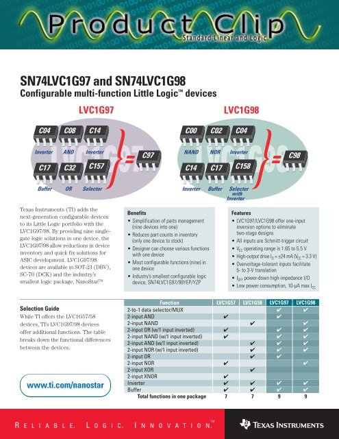
SN74<strong>LVC1G97</strong> and SN74<strong>LVC1G98</strong><br />
Configurable multi-function Little Logic TM<br />
devices<br />
C04 C08<br />
C17 C32<br />
C14<br />
Inverter AND Inverter<br />
C157<br />
Buffer OR Selector<br />
<strong>Texas</strong> <strong>Instruments</strong> (TI) adds the<br />
next-generation configurable devices<br />
to its Little Logic portfolio with the<br />
<strong>LVC1G97</strong>/98. By providing nine singlegate<br />
logic solutions in one device, the<br />
<strong>LVC1G97</strong>/98 allow reductions in device<br />
inventory and quick fix solutions for<br />
ASIC development. <strong>LVC1G97</strong>/98<br />
devices are available in SOT-23 (DBV),<br />
SC-70 (DCK) and the industry’s<br />
smallest logic package, NanoStar. TM<br />
Selection Guide<br />
While TI offers the LVC1G57/58<br />
devices, TI’s <strong>LVC1G97</strong>/98 devices<br />
offer additional functions. The table<br />
breaks down the functional differences<br />
between the devices.<br />
www.ti.com/nanostar<br />
<strong>LVC1G97</strong> <strong>LVC1G98</strong><br />
C97<br />
C00 C02<br />
C14 C17<br />
Benefits<br />
• Simplification of parts management<br />
(nine devices into one)<br />
• Reduces part counts in inventory<br />
(only one device to stock)<br />
• Designer can choose various functions<br />
with one device<br />
• Most configurable functions (nine) in<br />
one device<br />
• Industry’s smallest configurable logic<br />
device, SN74<strong>LVC1G97</strong>/98YEP/YZP<br />
C04<br />
NAND NOR Inverter<br />
C158<br />
Inverter Buffer Selector<br />
with<br />
Inverter<br />
R E L I A B L E. L O G I C. I N N O V A T I O N. TM<br />
C98<br />
Features<br />
• <strong>LVC1G97</strong>/<strong>LVC1G98</strong> offer one-input<br />
inversion options to eliminate<br />
two-stage designs<br />
• All inputs are Schmitt-trigger circuit<br />
•V CC operating range is 1.65 to 5.5 V<br />
• High-output drive I O = ±24 mA (V CC = 3.3 V)<br />
• Overvoltage-tolerant inputs facilitate<br />
5- to 3-V translation<br />
•I OFF power-down high-impedance I/O<br />
• Low power consumption, 10-µA max I CC<br />
Function LVC1G57 LVC1G58 <strong>LVC1G97</strong> <strong>LVC1G98</strong><br />
2-to-1 data selector/MUX ✔ ✔<br />
2-input AND ✔ ✔<br />
2-input NAND ✔ ✔<br />
2-input OR (w/1 input inverted) ✔ ✔ ✔<br />
2-input NAND (w/1 input inverted) ✔ ✔ ✔<br />
2-input AND (w/1 input inverted) ✔ ✔ ✔<br />
2-input NOR (w/1 input inverted) ✔ ✔ ✔<br />
2-input OR ✔ ✔<br />
2-input NOR ✔ ✔<br />
2-input XOR ✔<br />
2-input XNOR ✔<br />
Inverter ✔ ✔ ✔ ✔<br />
Buffer ✔ ✔ ✔ ✔<br />
Total functions in one package 7 7 9 9
Space-Saving Comparisons<br />
Besides the standard 2-input logic gate functions, the<br />
<strong>LVC1G97</strong>/98 both offer four additional functions. This allows<br />
functions that were once only achievable with two ICs to be<br />
embedded in one small chip. In turn, crucial board space is<br />
saved for more critical functions or for miniaturization.<br />
C14<br />
Inverter<br />
C14<br />
Inverter<br />
A<br />
B<br />
Inverter (04/14) + AND (08) Inverter (04/14) + OR (32)<br />
C08<br />
AND<br />
C00<br />
NAND<br />
C97<br />
C98<br />
C97<br />
C98<br />
C14<br />
Inverter<br />
C32<br />
OR<br />
C97<br />
C98<br />
Inverter (04/14) + NAND (00) Inverter (04/14) + NOR (02)<br />
GND<br />
VCC<br />
GND<br />
C14<br />
Inverter<br />
Board-Space Reduction<br />
Y<br />
C02<br />
NOR<br />
C97<br />
C98<br />
Inverter (04/14) + AND (08) <strong>LVC1G97</strong>/98<br />
A<br />
B<br />
GND<br />
VCC<br />
Y
Wiring Method and Truth Table for <strong>LVC1G97</strong>/98<br />
<strong>LVC1G97</strong> Configurations<br />
Input pins 1, 3 and 6 are for<br />
wiring, V CC = pin 5, GND =<br />
pin 2 and Y Output = pin 4.<br />
Any unwired pin should be<br />
connected to GND or V CC .<br />
B<br />
1<br />
2<br />
3<br />
6<br />
5<br />
4<br />
A<br />
Y<br />
VCC<br />
A<br />
B<br />
A<br />
B<br />
GND<br />
INPUTS OUTPUT<br />
Pin 6<br />
A<br />
Pin 1<br />
B<br />
Pin 3<br />
GND<br />
Y<br />
L L L L<br />
L L H L<br />
L H L H<br />
L H H H<br />
H L L L<br />
H L H H<br />
H H L L<br />
H H H H<br />
Y<br />
Y<br />
157: 2-to-1 Data Selector/MUX 08: 2-Input AND Gate<br />
VCC A/B<br />
VCC<br />
A<br />
B<br />
1<br />
2<br />
3<br />
6<br />
5<br />
4<br />
A/B<br />
Y<br />
A<br />
B<br />
Y<br />
B<br />
1<br />
2<br />
3<br />
6<br />
5<br />
4<br />
A<br />
Y<br />
A<br />
B<br />
GND GND<br />
INPUTS OUTPUT<br />
INPUTS OUTPUT<br />
Pin 6<br />
A/B<br />
Pin 1<br />
A<br />
Pin 3<br />
B<br />
Y<br />
Pin 6<br />
A<br />
Pin 1<br />
GND<br />
Pin 3<br />
B<br />
Y<br />
L L L L<br />
L L L L<br />
L L H L<br />
L L H L<br />
L H L H<br />
L H L H<br />
L H H H<br />
L H H H<br />
H L L L<br />
H L L L<br />
H L H H<br />
H L H H<br />
H H L L<br />
H H L L<br />
H H H H<br />
H H H H<br />
B<br />
1<br />
2<br />
3<br />
6<br />
5<br />
4<br />
A<br />
Y<br />
VCC<br />
A<br />
B<br />
Y<br />
1<br />
2<br />
3<br />
6<br />
5<br />
4<br />
A<br />
Y<br />
GND GND<br />
GND<br />
INPUTS OUTPUT<br />
INPUTS OUTPUT<br />
INPUTS OUTPUT<br />
Pin 6<br />
A<br />
Pin 1<br />
B<br />
Pin 3<br />
VCC Y<br />
Pin 6<br />
A<br />
Pin 1<br />
VCC Pin 3<br />
GND<br />
Y<br />
Pin 6<br />
GND<br />
Pin 1<br />
A<br />
Pin 3<br />
GND<br />
Y<br />
L L L L<br />
L L L L<br />
L L L L<br />
L L H L<br />
L L H L<br />
L L H L<br />
L H L H<br />
L H L H<br />
L H L H<br />
L H H H<br />
L H H H<br />
L H H H<br />
H L L L<br />
H L L L<br />
H L L L<br />
H L H H<br />
H L H H<br />
H L H H<br />
H H L L<br />
H H L L<br />
H H L L<br />
H H H H<br />
H H H H<br />
H H H H<br />
VCC<br />
A<br />
Y<br />
Y<br />
14+00/14+32: 2-Input OR/NAND<br />
Gate with One Inverted Input<br />
VCC<br />
1 6 A<br />
A<br />
B<br />
Y<br />
2 5<br />
B<br />
GND<br />
3 4 Y A<br />
B<br />
Y<br />
INPUTS OUTPUT<br />
Pin 6<br />
A<br />
Pin 1<br />
VCC Pin 3<br />
B<br />
Y<br />
L L L L<br />
L L H L<br />
L H L H<br />
L H H H<br />
H L L L<br />
H L H H<br />
H H L L<br />
H H H H<br />
14+02/14+08: 2-Input AND/NOR<br />
Gate with One Inverted Input 32: 2-Input OR Gate 04/14: Inverter 17/34: Noninverted Buffer<br />
<strong>LVC1G98</strong> Configurations<br />
Input pins 1, 3 and 6 are for<br />
wiring, V CC = pin 5, GND =<br />
pin 2 and Y Output = pin 4.<br />
Any unwired pin should be<br />
connected to GND or V CC .<br />
158: 2-to-1 Data Selector/MUX<br />
with Inverted Output 00: 2-Input NAND Gate<br />
VCC<br />
A/B<br />
VCC<br />
A<br />
B<br />
1<br />
2<br />
3<br />
6<br />
5<br />
4<br />
A/B<br />
Y<br />
A<br />
B<br />
Y<br />
B<br />
1<br />
2<br />
3<br />
6<br />
5<br />
4<br />
A<br />
Y<br />
A<br />
B<br />
GND GND<br />
INPUTS OUTPUT<br />
INPUTS OUTPUT<br />
Pin 6<br />
A/B<br />
Pin 1<br />
A<br />
Pin 3<br />
B<br />
Y<br />
Pin 6<br />
A<br />
Pin 1<br />
GND<br />
Pin 3<br />
B<br />
Y<br />
L L L H<br />
L L L H<br />
L L H H<br />
L L H H<br />
L H L L<br />
L H L L<br />
L H H L<br />
L H H L<br />
H L L H<br />
H L L H<br />
H L H L<br />
H L H L<br />
H H L H<br />
H H L H<br />
H H H L<br />
H H H L<br />
14+00/14+32: 2-Input NAND/OR<br />
Gate with One Inverted Input 02: 2-Input NOR Gate 17: Noninverted Buffer 04/14: Inverter<br />
B<br />
1<br />
2<br />
3<br />
6<br />
5<br />
4<br />
A<br />
VCC<br />
A<br />
B<br />
Y A<br />
B<br />
GND<br />
INPUTS OUTPUT<br />
Pin 6<br />
A<br />
Pin 1<br />
B<br />
Pin 3<br />
GND<br />
Y<br />
L L L H<br />
L L H H<br />
L H L L<br />
L H H L<br />
H L L H<br />
H L H L<br />
H H L H<br />
H H H L<br />
Y<br />
Y<br />
B<br />
1<br />
2<br />
3<br />
6<br />
5<br />
4<br />
A<br />
Y<br />
VCC<br />
A<br />
B<br />
Y<br />
1<br />
2<br />
3<br />
6<br />
5<br />
4<br />
A<br />
Y<br />
GND<br />
GND<br />
GND<br />
INPUTS OUTPUT<br />
INPUTS OUTPUT<br />
INPUTS OUTPUT<br />
Pin 6<br />
A<br />
Pin 1<br />
B<br />
Pin 3<br />
VCC<br />
Y<br />
Pin 6<br />
A<br />
Pin 1<br />
VCC<br />
Pin 3<br />
GND<br />
Y<br />
Pin 6<br />
GND<br />
Pin 1<br />
A<br />
Pin 3<br />
GND<br />
Y<br />
L L L H<br />
L L L H<br />
L L L H<br />
L L H H<br />
L L H H<br />
L L H H<br />
L H L L<br />
L H L L<br />
L H L L<br />
L H H L<br />
L H H L<br />
L H H L<br />
H L L H<br />
H L L H<br />
H L L H<br />
H L H L<br />
H L H L<br />
H L H L<br />
H H L H<br />
H H L H<br />
H H L H<br />
H H H L<br />
H H H L<br />
H H H L<br />
VCC<br />
A<br />
Y<br />
Y<br />
A<br />
1<br />
2<br />
3<br />
6<br />
5<br />
4<br />
Y<br />
Y<br />
VCC<br />
14+02/14+08: 2-Input NOR/AND<br />
Gate with One Inverted Input<br />
VCC<br />
1 6 A<br />
A<br />
B<br />
Y<br />
2 5<br />
B<br />
GND<br />
3 4 Y A<br />
B<br />
Y<br />
INPUTS OUTPUT<br />
Pin 6<br />
A<br />
Pin 1<br />
VCC<br />
Pin 3<br />
B<br />
Y<br />
L L L H<br />
L L H H<br />
L H L L<br />
L H H L<br />
H L L H<br />
H L H L<br />
H H L H<br />
H H H L<br />
A<br />
1<br />
2<br />
3<br />
6<br />
5<br />
4<br />
VCC<br />
A<br />
A<br />
Y<br />
Y
Packaging Options<br />
DBV (SOT-23)<br />
(Actual Size)<br />
Little Logic<br />
0,95 mm<br />
2,90 mm<br />
2,80 mm<br />
Lead Frame<br />
Reliable. Logic. Innovation.; the red/black banner; NanoStar;<br />
NanoFree and Little Logic are trademarks of <strong>Texas</strong> <strong>Instruments</strong>.<br />
© 2003 <strong>Texas</strong> <strong>Instruments</strong> Incorporated<br />
Printed in the U.S.A. by _____________________________<br />
Printed on recycled paper.<br />
DCK (SC-70)<br />
5-pin or 6-pin 5-pin or 6-pin<br />
(Actual Size)<br />
Little Logic<br />
2,0 mm<br />
TI Worldwide Technical Support<br />
Internet<br />
TI Semiconductor Product Information Center Home Page<br />
support.ti.com<br />
TI Semiconductor KnowledgeBase Home Page<br />
support.ti.com/sc/knowledgebase<br />
Product Information Centers<br />
Americas<br />
Phone +1(972) 644-5580<br />
Fax +1(972) 927-6377<br />
Internet/Email support.ti.com/sc/pic/americas.htm<br />
Europe, Middle East, and Africa<br />
Phone<br />
Belgium (English) +32 (0) 27 45 55 32<br />
Finland (English) +358 (0) 9 25173948<br />
France +33 (0) 1 30 70 11 64<br />
Germany +49 (0) 8161 80 33 11<br />
Israel (English) 1800 949 0107<br />
Italy 800 79 11 37<br />
Netherlands (English) +31 (0) 546 87 95 45<br />
Spain +34 902 35 40 28<br />
Sweden (English) +46 (0) 8587 555 22<br />
United Kingdom +44 (0) 1604 66 33 99<br />
Fax +(49) (0) 8161 80 2045<br />
Email epic@ti.com<br />
Internet support.ti.com/sc/pic/euro.htm<br />
2,10 mm<br />
0,65 mm<br />
Important Notice: The products and services of <strong>Texas</strong> <strong>Instruments</strong><br />
Incorporated and its subsidiaries described herein are sold subject to TI’s<br />
standard terms and conditions of sale. Customers are advised to obtain the most<br />
current and complete information about TI products and services before placing<br />
orders. TI assumes no liability for applications assistance, customer’s<br />
applications or product designs, software performance, or infringement of<br />
patents. The publication of information regarding any other company’s products<br />
or services does not constitute TI’s approval, warranty or endorsement thereof.<br />
NanoStar TM<br />
(YEP)<br />
5-pin or 6-pin<br />
(Actual Size)<br />
NanoFree TM<br />
(YZP)<br />
Wafer Chip-Scale<br />
0,5 mm<br />
1,4 mm<br />
0,9 mm<br />
For more information on samples, datasheets, application<br />
reports and design summaries, visit:<br />
www.ti.com/sc/device/SN74<strong>LVC1G97</strong><br />
www.ti.com/sc/device/SN74<strong>LVC1G98</strong><br />
logic.ti.com<br />
Industry’s<br />
Smallest<br />
Configurable<br />
Logic Device<br />
Japan<br />
Fax International +81-3-3344-5317<br />
Domestic 0120-81-0036<br />
Internet/Email International support.ti.com/sc/pic/japan.htm<br />
Domestic www.tij.co.jp/pic<br />
Asia<br />
Phone<br />
International +886-2-23786800<br />
Domestic Toll-Free Number<br />
Australia 1-800-999-084<br />
China 108-00-886-0015<br />
Hong Kong 800-96-5941<br />
Indonesia 001-803-8861-1006<br />
Korea 080-551-2804<br />
Malaysia 1-800-80-3973<br />
New Zealand 0800-446-934<br />
Philippines 1-800-765-7404<br />
Singapore 800-886-1028<br />
Taiwan 0800-006800<br />
Thailand 001-800-886-0010<br />
Fax 886-2-2378-6808<br />
Email tiasia@ti.com<br />
Internet support.ti.com/sc/pic/asia.htm B010203<br />
Safe Harbor Statement<br />
This publication contains forward-looking statements that involve a number of risks and uncertainties. These<br />
“forward-looking statements” are intended to qualify for the safe harbor from liability established by the Private<br />
Securities Litigation Reform Act of 1995. These forward-looking statements generally can be identified by phrases<br />
such as TI or its management “believes,” “expects,” “anticipates,” “foresees,” “forecasts,” “estimates” or other<br />
words or phrases of similar import. Similarly, such statements herein that describe the company's products,<br />
business strategy, outlook, objectives, plans, intentions or goals also are forward-looking statements. All such<br />
forward-looking statements are subject to certain risks and uncertainties that could cause actual results to differ<br />
materially from those in forward-looking statements. Please refer to TI's most recent Form 10-K for more<br />
information on the risks and uncertainties that could materially affect future results of operations. We disclaim any<br />
intention or obligation to update any forward-looking statements as a result of developments occurring after the<br />
date of this publication.<br />
SCYB010