WAVES AND VIBRATIONS IN INHOMOGENEOUS STRUCTURES ...
WAVES AND VIBRATIONS IN INHOMOGENEOUS STRUCTURES ...
WAVES AND VIBRATIONS IN INHOMOGENEOUS STRUCTURES ...

Create successful ePaper yourself
Turn your PDF publications into a flip-book with our unique Google optimized e-Paper software.
nanoimprinted patterns are transferred into the top 340 nm thick silicon layer of the SOI wafer<br />
by using an optimized SF6-based inductively coupled plasma (ICP) RIE. The etch-selectivity<br />
is 9:1 (silicon:mr-I T85) [24] which allows for pattern transfer of the imprinted holes through<br />
the device silicon layer of the SOI wafer.<br />
3. Straight photonic crystal waveguides<br />
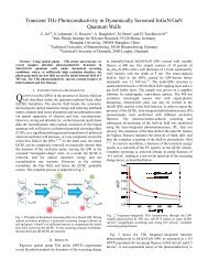
Figure 1 (left) shows a scanning electron microscope (SEM) image of the central part of a<br />
NIL fabricated SOI device consisting of a W1 PhCW connected to ordinary tapered ridge<br />
waveguides. The photonic crystal part of the waveguide is 10 μm long, the pitch of the<br />
hexagonal crystal lattice 400 nm, and the hole diameter 250 nm. The width of the ridge<br />
waveguides are adiabatically tapered over 450 μm from 4 μm at the end facets of the sample<br />
down to 1 μm at the interface to the crystal waveguide. The etch patterns seen to the right and<br />
left of the PhCW are caused by the controlled flow of excess polymer during the imprint<br />
process. The excess polymer is a result from the large variation in pattern density between the<br />
PhCW area and the surrounding un-patterned regions. The polymer flow does not represent an<br />
issue in the fabrication of high-quality photonic circuits with more complex design. The<br />
excess polymer flow can easily be controlled by adding dummy structures to equalize the<br />
pattern density. Also, the fabrication of more complex and/or high-density photonic circuits<br />
will typically reduce the variation in the pattern density, and thus simplify the control of the<br />
polymer flow.<br />
The fabricated waveguides have been characterized by optical transmission<br />
measurements using quasi-transverse electric (TE) polarized light from a laser source in the<br />
wavelength region from 1520–1620 nm (<strong>AND</strong>O AQ4321D) and broadband light emitting<br />
diodes (<strong>AND</strong>O AQ4222) covering the wavelength range 1360–1620 nm. Figure 1 (right)<br />
shows the resulting laser transmission spectrum. The spectrum exhibits the characteristics of a<br />
W1 PhCW having a sharp and well-defined transition (around 1590 nm) between the low-loss<br />
guided defect mode and the photonic band gap. The observed sharp cut-off and the high and<br />
uniform transmission level below the cut-off wavelength of the spectrum are similar to results<br />
obtained for PhCWs of similar designs fabricated by EBL [17] and DUVL [6]. The ripples in<br />
the spectrum (zoom-in shown in the inset) are due to Fabry-Pérot oscillations caused by<br />
reflections from the end facets of the sample.<br />
NORMALISED TRANSMISSION (dB)<br />
0<br />
-10<br />
-20<br />
-30<br />
0<br />
-5<br />
-10<br />
1585 1588 1591<br />
-40<br />
1520 1540 1560 1580 1600 1620<br />
WAVELENGTH (nm)<br />
Fig. 1. (Left) SEM image of a photonic wire adjacent to a 10 μm long W1 PhCW fabricated in<br />
SOI by NIL. The etch patterns seen on the outer sides are caused by the controlled flow of<br />
excess polymer during the imprint process. (Right): Measured transmission spectrum for quasi-<br />
TE polarized laser light through the structure. Inset shows a zoom-in on the spectrum.<br />
4. Topology optimized nanophotonic devices<br />
Recently, we have proposed a novel inverse design strategy called topology optimization<br />
(TO), which allows for designing nanophotonic structures with enhanced functionalities [25].<br />
In some cases, this inverse design method proposes optimized designs with feature sizes down<br />
to ~30 nm. Hence, such structures are very challenging to fabricate even with EBL and will<br />
serve as excellent benchmarks for pattern replication fidelity in the NIL fabrication process.<br />
#76773 - $15.00 USD Received 6 November 2006; revised 18 January 2007; accepted 19 January 2007<br />
(C) 2007 OSA 5 February 2007 / Vol. 15, No. 3 / OPTICS EXPRESS 1264