WAVES AND VIBRATIONS IN INHOMOGENEOUS STRUCTURES ...
WAVES AND VIBRATIONS IN INHOMOGENEOUS STRUCTURES ...
WAVES AND VIBRATIONS IN INHOMOGENEOUS STRUCTURES ...

You also want an ePaper? Increase the reach of your titles
YUMPU automatically turns print PDFs into web optimized ePapers that Google loves.
1204 IEEE PHOTONICS TECHNOLOGY LETTERS, VOL. 17, NO. 6, JUNE 2005<br />
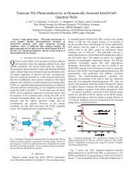
Fig. 4. (a) Fabricated generic structure and (b) the topology optimized double<br />
90 waveguide bend.<br />
Fig. 5. Measured bend loss for the fabricated generic and optimized waveguide<br />
component.<br />
e-beam lithography and standard anisotropic reactive-ion etch.<br />
The PhCs are defined as air holes in a triangular lattice and<br />
the PhCWs are carved out by removing a single row of holes<br />
in the nearest-neighbor direction of the crystal lattice. We use<br />
lattice pitch nm, diameter of the holes nm,<br />
and thickness of the Si–SiO layers 340 nm/1 m. This configuration<br />
displays a broad PBG below the silica-line from<br />
0.2592 to 0.3436 (normalized frequency) and allows TE-polarized<br />
single-mode propagation in the PhCWs. The fabricated<br />
topology-optimized structure is shown in Fig. 4(b) and it nicely<br />
resembles the designed structure [Fig. 3(d)].<br />
The fabricated PhCWs were optically characterized using<br />
broad-band light-emitting diodes (LEDs) as sources. Three<br />
different LEDs centered around 1310, 1414, and 1538 nm were<br />
used to cover the full bandwidth of the fabricated components<br />
and tapered lensed fibers were used to couple light in and<br />
out of the ridge waveguides connected to the PhCWs. Two<br />
polarization controllers and a polarizer with an extinction<br />
ratio better than 35 dB were used to control the polarization<br />
of the light sent into the device. The optical spectra for the<br />
transmitted light were recorded with a spectral resolution of<br />
10 nm using an optical spectrum analyzer. To extract the bend<br />
loss, the transmission spectra have been normalized to the<br />
transmission spectrum for a straight PhCW of similar length.<br />
Fig. 5 shows the measured bend loss of TE-polarized light for<br />
the generic structure and the topology-optimized structure. A<br />
transmission loss of 1 dB/bend is obtained for the wavelength<br />
range 1250–1450 nm.<br />
IV. CONCLUSION<br />
We have used the method of topology optimization to design<br />
a double 90 bend in a photonic crystal waveguide based on a<br />
triangular configuration of air holes. The waveguide was fabricated<br />
in SOI and showed a very low bend loss for TE-polarized<br />
light of less than 1 dB per bend in a broad wavelength range of<br />
200 nm.<br />
The fabricated device adds to the existing collection of highperformance<br />
photonic crystal building blocks that display lowloss<br />
over a broad wavelength. The good performance makes<br />
these components natural parts of the realization of PICs based<br />
on photonic crystals.<br />
REFERENCES<br />
[1] M. P. Bendsøe and N. Kikuchi, “Generating optimal topologies in structural<br />
design using a homogenization method,” Comput. Methods Appl.<br />
Mech. Eng., vol. 71, no. 2, pp. 197–224, 1988.<br />
[2] M. P. Bendsøe and O. Sigmund, Topology Optimization—Theory,<br />
Methods and Applications. Berlin, Germany: Springer-Verlag, 2003.<br />
[3] J. D. Joannopoulos, R. D. Meade, and J. N. Winn, Photonic Crystals.<br />
Princeton, NJ: Princeton Univ. Press, 1995.<br />
[4] Y. Sugimoto, Y. Tanaka, N. Ikeda, K. Kanamoto, Y. Nakamura, S.<br />
Ohkouchi, H. Nakamura, K. Inoue, H. Sasaki, Y. Watanabe, K. Ishida,<br />
H. Ishikawa, and K. Asakawa, “Two dimensional semiconductor-based<br />
photonic crystal slab waveguides for ultra-fast optical signal processing<br />
devices,” IEICE Trans. Electron., vol. E87-C, pp. 316–327, 2004.<br />
[5] A. Chutinan, M. Okano, and S. Noda, “Wider bandwidth with high transmission<br />
through waveguide bends in two-dimensional photonic crystal<br />
slabs,” Appl. Phys. Lett., vol. 80, pp. 1698–1700, 2002.<br />
[6] A. Talneau, L. L. Gouezigou, N. Bouadma, M. Kafesaki, C. M. Soukoulis,<br />
and M. Agio, “Photonic-crystal ultrashort bends with improved<br />
transmission and low reflection at 1.55 "m,” Appl. Phys. Lett., vol. 80,<br />
pp. 547–549, 2002.<br />
[7] R. Wilson, T. J. Karle, I. Moerman, and T. F. Krauss, “Efficient photonic<br />
crystal Y-junctions,” J. Opt. A, Pure Appl. Opt., vol. 5, pp. 76–80, 2003.<br />
[8] P. I. Borel, L. H. Frandsen, A. Harpøth, J. B. Leon, H. Liu, M. Kristensen,<br />
W. Bogaerts, P. Dumon, R. Baets, V. Wiaux, J. Wouters, and S.<br />
Beckx, “Bandwidth engineering of photonic crystal waveguide bends,”<br />
Electron. Lett., vol. 40, pp. 1263–1264, 2004.<br />
[9] P. I. Borel, A. Harpøth, L. H. Frandsen, M. Kristensen, P. Shi, J. S.<br />
Jensen, and O. Sigmund, “Topology optimization and fabrication of photonic<br />
crystal structures,” Opt. Express, vol. 12, no. 9, pp. 1996–2001,<br />
2004.<br />
[10] L. H. Frandsen, A. Harpøth, P. I. Borel, M. Kristensen, J. S. Jensen,<br />
and O. Sigmund, “Broadband photonic crystal waveguide 60 bend obtained<br />
utilizing topology optimization,” Opt. Express, vol. 12, no. 24,<br />
pp. 5916–5921, 2004.<br />
[11] P. I. Borel, L. H. Frandsen, A. Harpøth, M. Kristensen, J. S. Jensen,<br />
and O. Sigmund, “Topology optimized broadband photonic crystal<br />
Y-splitter,” Electron. Lett., vol. 41, no. 2, pp. 69–71, 2005.<br />
[12] M. Koshiba, Y. Tsuji, and S. Sasaki, “High-performance absorbing<br />
boundary conditions for photonic crystal waveguide simulations,” IEEE<br />
Microw. Wireless Components Lett., vol. 11, no. 4, pp. 152–154, Apr.<br />
2001.<br />
[13] J. S. Jensen and O. Sigmund, “Topology optimization of photonic crystal<br />
structures: a high-bandwidth low-loss T-junction waveguide,” J. Opt.<br />
Soc. Amer. B, to be published.<br />
[14] K. Svanberg, “The method of moving asymptotes—a new method<br />
for structural optimization,” Int. J. Numer. Methods Eng., vol. 24, pp.<br />
359–373, 1987.<br />
[15] J. Jin, The Finite Element Method in Electromagnetics, 2nd ed. New<br />
York: Wiley, 2002.