WAVES AND VIBRATIONS IN INHOMOGENEOUS STRUCTURES ...
WAVES AND VIBRATIONS IN INHOMOGENEOUS STRUCTURES ...
WAVES AND VIBRATIONS IN INHOMOGENEOUS STRUCTURES ...

Create successful ePaper yourself
Turn your PDF publications into a flip-book with our unique Google optimized e-Paper software.
JENSEN et al.: TOPOLOGY DESIGN <strong>AND</strong> FABRICATION OF AN EFFICIENT DOUBLE 90 PHOTONIC CRYSTAL WAVEGUIDE BEND 1203<br />
II. OPTIMIZATION<br />
The method of topology optimization is used to modify the<br />
distribution between the dielectric and air in the designated<br />
design area shown in Fig. 1(b). The optimization algorithm is<br />
based on a two-dimensional (2-D) frequency-domain solver<br />
based on a finite element discretization that yields the following<br />
equations for TE-polarized light:<br />
in which is a wave input vector, is a vector containing the<br />
discretized nodal values of the out-of-plane magnetic field ,<br />
and is the system matrix with an explicit dependence on the<br />
wave frequency , and the position-dependent dielectric constant<br />
. Here, is the plane position vector.<br />
Each unit cell is discretized using 14 12 four-noded quadrilateral<br />
elements. This discretization is sufficient for describing<br />
the geometry satisfactorily, and for capturing the dynamic<br />
behavior with adequate accuracy. The full computational model<br />
consists of the domain shown in Fig. 1(a) as well as additional<br />
perfectly matching layers [12] and comprises in total about<br />
115 000 elements of which 6720 are within the design domain.<br />
A single design variable is now introduced in each finite<br />
element within the design domain, and is assumed to be element-wise<br />
constant and to depend explicitly on as follows:<br />
where<br />
Thus, we let the design variable in each element govern the material<br />
properties of the element, in such a way that if ,<br />
the dielectric constant of that element is one, and with<br />
it takes the value .<br />
We use continuous design variables to allow for using a<br />
gradient-based optimization strategy. The optimization method<br />
is described in detail in [2] and [13] and will only be briefly<br />
outlined here; as the goal for the optimization algorithm,<br />
we wish to find the material distribution that maximizes the<br />
transmitted power evaluated at the output port , which<br />
is computed based on the solution to (1). Based on the sensitivities<br />
, computed analytically, a mathematical<br />
programming tool MMA [14] is then used to change the material<br />
distribution in an iterative process until cannot be<br />
further improved.<br />
Since the design variables are continuous and not discrete, the<br />
possibility for elements in the final design with values between<br />
zero and one, so-called “gray” elements, is present. This corresponds<br />
to an intermediate “porous” material which is not feasible<br />
from a fabrication point of view. Several techniques have<br />
been developed to remedy this problem [2], but here we use a<br />
method specially designed for photonic waveguides [13], in that<br />
we artificially make design variables between zero and one induce<br />
additional conduction , in the following form:<br />
which enters (1) as an additional imaginary term in the system<br />
matrix and causes dissipation of energy. In this way, gray elements<br />
will be “un-economical” and will, thus, be forced toward<br />
(1)<br />
(2)<br />
(3)<br />
(4)<br />
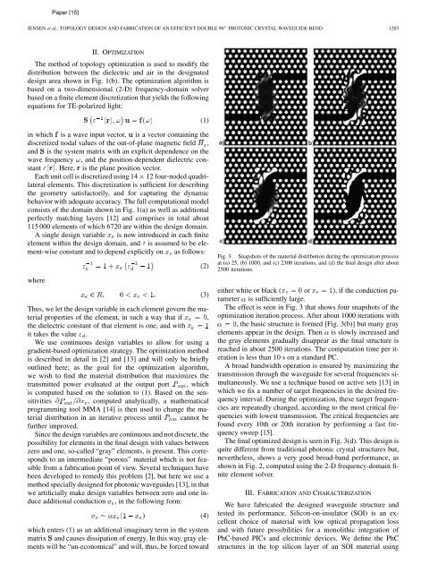
Fig. 3. Snapshots of the material distribution during the optimization process<br />
at (a) 25, (b) 1000, and (c) 2300 iterations, and (d) the final design after about<br />
2500 iterations.<br />
either white or black ( or ), if the conduction parameter<br />
is sufficiently large.<br />
The effect is seen in Fig. 3 that shows four snapshots of the<br />
optimization iteration process. After about 1000 iterations with<br />
, the basic structure is formed [Fig. 3(b)] but many gray<br />
elements appear in the design. Then is slowly increased and<br />
the gray elements gradually disappear as the final structure is<br />
reached in about 2500 iterations. The computation time per iteration<br />
is less than 10 s on a standard PC.<br />
A broad bandwidth operation is ensured by maximizing the<br />
transmission through the waveguide for several frequencies simultaneously.<br />
We use a technique based on active sets [13] in<br />
which we fix a number of target frequencies in the desired frequency<br />
interval. During the optimization, these target frequencies<br />
are repeatedly changed, according to the most critical frequencies<br />
with lowest transmission. The critical frequencies are<br />
found every 10th or 20th iteration by performing a fast frequency<br />
sweep [15].<br />
The final optimized design is seen in Fig. 3(d). This design is<br />
quite different from traditional photonic crystal structures but,<br />
nevertheless, shows a very good broad-band performance, as<br />
shown in Fig. 2, computed using the 2-D frequency-domain finite<br />
element solver.<br />
III. FABRICATION <strong>AND</strong> CHARACTERIZATION<br />
We have fabricated the designed waveguide structure and<br />
tested its performance. Silicon-on-insulator (SOI) is an excellent<br />
choice of material with low optical propagation loss<br />
and with future possibilities for a monolithic integration of<br />
PhC-based PICs and electronic devices. We define the PhC<br />
structures in the top silicon layer of an SOI material using