WAVES AND VIBRATIONS IN INHOMOGENEOUS STRUCTURES ...
WAVES AND VIBRATIONS IN INHOMOGENEOUS STRUCTURES ...
WAVES AND VIBRATIONS IN INHOMOGENEOUS STRUCTURES ...

Create successful ePaper yourself
Turn your PDF publications into a flip-book with our unique Google optimized e-Paper software.
J. S. Jensen and O. Sigmund Vol. 22, No. 6/June 2005/J. Opt. Soc. Am. B 1197<br />
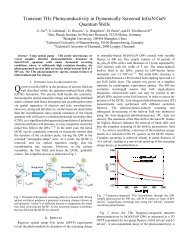
Fig. 9. Design optimized for frequency range ˜ =0.32–0.44 with<br />
an enlarged design domain. The field is computed for ˜ =0.38.<br />
Fig. 10. Transmission spectra for the design optimized for the<br />
entire frequency range ˜ =0.32–0.44. Shown also is the spectrum<br />
for the design optimized for ˜ =0.38.<br />
tion of material in a design domain near the junction. By<br />
maximizing the power transmission through the two<br />
waveguide output ports, we obtain designs with vanishing<br />
reflection at the junction.<br />
We obtained a high transmission locally by performing<br />
the optimization for single frequencies. To get a larger<br />
bandwidth with high transmission, we introduced an<br />
active-set strategy in which the transmission is maximized<br />
for several frequencies simultaneously and in<br />
which these target frequencies are repeatedly updated<br />
with fast frequency sweeps to identify the most critical<br />
frequencies with lowest transmission. It was shown that,<br />
by increasing the design domain, we obtained a better<br />
performance in a larger frequency range, approaching full<br />
transmission for the entire frequency range under consideration.<br />
To avoid local maxima based on local resonance effects,<br />
we applied a continuation method by convexifying the object<br />
and response functions with artificial damping. Additionally,<br />
we introduced a scheme to avoid values of the<br />
continuous design variable between 0 and 1, correspond-<br />
ing to intermediate material. This was done by penalizing<br />
these intermediate values with extra artificial damping.<br />
The algorithm appears to be a robust and efficient design<br />
tool for PhC components. Although based on a 2D<br />
model, recent experience with manufactured structures 5<br />
indicates that good performance of the actual devices can<br />
be expected, and the optimization scheme can directly be<br />
implemented with a three-dimensional computational<br />
model to address the important issue of out-of-plane scattering.<br />
Additionally, the objective function can easily be<br />
modified to deal with other functionalities.<br />
ACKNOWLEDGMENTS<br />
The authors thank Martin P. Bendsøe for valuable comments<br />
and suggestions. The work was supported by the<br />
Danish Technical Research Council through the grant<br />
“Designing bandgap materials and structures with optimized<br />
dynamic properties.”<br />
J. S. Jensen, the corresponding author, can be reached<br />
by e-mail at jsj@mek.dtu.dk.<br />
REFERENCES<br />
1. E. Yablonovitch, “Inhibited spontaneous emission in solidstate<br />
physics and electronics,” Phys. Rev. Lett. 58,<br />
2059–2062 (1987).<br />
2. S. John, “Strong localization of photons in certain<br />
disordered dielectric superlattices,” Phys. Rev. Lett. 58,<br />
2486–2489 (1987).<br />
3. M. Burger, S. J. Osher, and E. Yablonovitch, “Inverse<br />
problem techniques for the design of photonic crystals,”<br />
IEICE Trans. Electron. E87-C, 258–265 (2004).<br />
4. J. S. Jensen and O. Sigmund, “Systematic design of<br />
photonic crystal structures using topology optimization:<br />
low-loss waveguide bends,” Appl. Phys. Lett. 84, 2022–2024<br />
(2004).<br />
5. P. I. Borel, A. Harpøth, L. H. Frandsen, M. Kristensen, P.<br />
Shi, J. S. Jensen, and O. Sigmund, “Topology optimization<br />
and fabrication of photonic crystal structures,” Opt.<br />
Express 12, 1996–2001 (2004).<br />
6. K. B. Chung, J. S. Yoon, and G. H. Song, “Analysis of<br />
optical splitters in photonic crystals,” in Photonic Bandgap<br />
Material and Devices, A. Adibi, A. Scherer, and S.-Yu. Lin,<br />
eds., Proc. SPIE 4655, 349–355 (2002).<br />
7. J. Smajic, C. Hafner, and D. Erni, “Optimization of<br />
photonic crystal structures,” J. Opt. Soc. Am. A 21,<br />
2223–2232 (2004).<br />
8. W. J. Kim and J. D. O’Brien, “Optimization of a twodimensional<br />
photonic-crystal waveguide branch by<br />
simulated annealing and the finite-element method,” J.<br />
Opt. Soc. Am. B 21, 289–295 (2004).<br />
9. T. Felici and T. F. G. Gallagher, “Improved waveguide<br />
structures derived from new rapid optimization<br />
techniques,” in Physics and Simulation of Optoelectronic<br />
Devices XI, M. Osinski, H. Amano, and P. Blood, eds., Proc.<br />
SPIE 4986, 375–385 (2003).<br />
10. M. P. Bendsøe and N. Kikuchi, “Generating optimal<br />
topologies in structural design using a homogenization<br />
method,” Comput. Methods Appl. Mech. Eng. 71, 197–224<br />
(1988).<br />
11. H. L. Thomas, M. Zhou, and U. Schramm, “Issues of<br />
commercial optimization software development,” Struct.<br />
Multidiscip. Optim. 23, 97–110 (2002).<br />
12. M. P. Bendsøe and O. Sigmund, Topology Optimization—<br />
Theory, Methods and Applications (Springer, Berlin, 2003).<br />
13. O. Sigmund and J. S. Jensen, “Systematic design of<br />
phononic band-gap materials and structures by topology