WAVES AND VIBRATIONS IN INHOMOGENEOUS STRUCTURES ...
WAVES AND VIBRATIONS IN INHOMOGENEOUS STRUCTURES ...
WAVES AND VIBRATIONS IN INHOMOGENEOUS STRUCTURES ...

Create successful ePaper yourself
Turn your PDF publications into a flip-book with our unique Google optimized e-Paper software.
2024 Appl. Phys. Lett., Vol. 84, No. 12, 22 March 2004 J. S. Jensen and O. Sigmund<br />
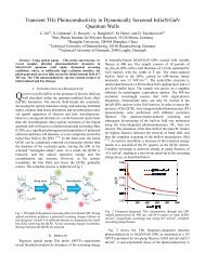
FIG. 3. a Optimized corner design, b postprocessed design with black<br />
and white elements only, and c transmission losses for the two designs and<br />
for a standard corner design.<br />
ing a mathematical programming solver MMA extra geometric<br />
or behavioral constraints can easily be added to<br />
Eq. 6.<br />
In our example we maximize the output energy for three<br />
frequencies ¯0.34,0.38,0.42(2c/a) in order to minimize<br />
the loss in a large frequency range. Figure 3a shows the<br />
optimized design obtained after about 500 iterations of the<br />
optimization algorithm about 20 s per iteration on a 2.66<br />
GHz computer. It is evident that the optimized design is<br />
practically ‘‘black–white,’’ i.e., almost free of elements with<br />
intermediate x i values between 0 and 1. In Fig. 3b is shown<br />
a postprocessed design where the few intermediate values<br />
that do appear are forced to either 0 or 1 with a simple filter.<br />
Figure 3c shows the transmission loss for the optimized<br />
and for the postprocessed designs. Noticeable is that a loss<br />
below 0.3% is obtained in the entire frequency range from<br />
0.325 to 0.440(2c/a).<br />
Although low transmission loss is obtained using a twodimensional<br />
model, the question of out-of-plane losses for<br />
the optimized waveguide remains open and should be addressed<br />
using a three-dimensional 3D model the optimization<br />
algorithm can immediately be used with a 3D model.<br />
However, the method is naturally also applicable to the design<br />
of waveguides based on holes in a dielectric and these<br />
are generally known to be less prone to out-of-plane losses.<br />
In addition to waveguide bends the method can be applied to<br />
systematic design of a large variety of optical devices such<br />
as, e.g., wave-splitters, multiplexers, and other more complex<br />
objectives. Future work will address these issues and we<br />
are also expecting to test optimized devices experimentally<br />
in the near future. Previous work by the authors has considered<br />
design of similar devices for elastic waves. 12<br />
This work was supported by the Danish technical<br />
research council STVF.<br />
1 J. D. Joannopoulos, R. D. Meade, and J. N. Winn, Photonic Crystals<br />
Princeton University Press, Princeton, NJ, 1995.<br />
2 K. Sakoda, Optical Properties of Photonic Crystals Springer, Berlin,<br />
2001.<br />
3 A. Mekis, J. C. Chen, I. Kurland, S. Fan, P. R. Villeneuve, and J. D.<br />
Joannopoulos, Phys. Rev. Lett. 77, 3787 1996.<br />
4 J. Moosburger, M. Kamp, A. Forchel, S. Olivier, H. Benisty, C. Weisbuch,<br />
and U. Oesterle, Appl. Phys. Lett. 79, 3579 2001.<br />
5 W. S. Mohammed, E. G. Johnson, and L. Vaissie, Proc. SPIE 4291, 65<br />
2001.<br />
6 J. Smajic, C. Hafner, and D. Erni, Opt. Express 11, 13782003.<br />
7 M. P. Bendsøe and N. Kikuchi, Comput. Methods Appl. Mech. Eng. 71,<br />
197 1988.<br />
8 M. P. Bendsøe and O. Sigmund, Topology Optimization Springer, Berlin,<br />
2003.<br />
9 M. Koshiba, Y. Tsuji, and S. Sasaki, IEEE Microw. Wirel. Compon. Lett.<br />
11, 152 2001.<br />
10 Y. Naka and H. Ikuno, International Symposium on Antennas and Propagation<br />
ISAP2000, Fukuoka, Japan, 2000, p. 787.<br />
11 K. Svanberg, Int. J. Numer. Methods Eng. 24, 359 1987.<br />
12 O. Sigmund and J. S. Jensen, Proc. R. Soc. London, Ser. A 361, 1001<br />
Downloaded 28 Jul 2009 to 192.38.67.112. Redistribution subject to AIP license or copyright; see http://apl.aip.org/apl/copyright.jsp<br />
2003.