WAVES AND VIBRATIONS IN INHOMOGENEOUS STRUCTURES ...
WAVES AND VIBRATIONS IN INHOMOGENEOUS STRUCTURES ...
WAVES AND VIBRATIONS IN INHOMOGENEOUS STRUCTURES ...

Create successful ePaper yourself
Turn your PDF publications into a flip-book with our unique Google optimized e-Paper software.
APPLIED PHYSICS LETTERS VOLUME 84, NUMBER 12 22 MARCH 2004<br />
Systematic design of photonic crystal structures using topology<br />
optimization: Low-loss waveguide bends<br />
Jakob S. Jensen a) and Ole Sigmund<br />
Department of Mechanical Engineering, Solid Mechanics, Nils Koppels Allé, Building 404,<br />
Technical University of Denmark, 2800 Kgs. Lyngby, Denmark<br />
Received 26 August 2003; accepted 25 January 2004<br />
Topology optimization is a promising method for systematic design of optical devices. As an<br />
example, we demonstrate how the method can be used to design a 90° bend in a two-dimensional<br />
photonic crystal waveguide with a transmission loss of less than 0.3% in almost the entire frequency<br />
range of the guided mode. The method can directly be applied to the design of other optical devices,<br />
e.g., multiplexers and wave splitters, with optimized performance. © 2004 American Institute of<br />
Physics. DOI: 10.1063/1.1688450<br />
A range of perspectives exist for using photonic crystal<br />
PC based waveguides in optical components. This has led<br />
to a considerable research interest in the design of waveguide<br />
bends with low transmission loss.<br />
PCs can be created by periodic arrangements of materials<br />
with different dielectric properties such as, e.g., dielectric<br />
columns in air or holes in a dielectric base material. 1 Such<br />
two-dimensional periodic configurations may forbid the<br />
propagation of plane polarized light in specific frequency<br />
ranges, i.e., the so-called photonic band gaps PBGs. A<br />
waveguide can be created by removing one or several lines<br />
of columns or holes resulting in defects that support guided<br />
modes in the PC structure. 2<br />
A key advantage of PC waveguides is that bends can be<br />
created with very little or no transmission loss even with<br />
bend curvatures as small as the wavelength. Although PC<br />
waveguides generally offer low losses compared to traditional<br />
dielectric waveguides, much effort has been devoted to<br />
reducing these losses to a minimum over larger frequency<br />
ranges. Waveguides with dielectric columns in a rectangular<br />
configuration have been subjected to extensive<br />
computations 3 and recently waveguides with holes etched in<br />
a triangular pattern in a dielectric have been analyzed thoroughly<br />
both theoretically and experimentally. 4<br />
Despite the considerable amount of studies on PC<br />
waveguides that have appeared, few papers have dealt with<br />
optimization or the inverse problem of obtaining structures<br />
with optimal or desired properties. The few papers that have<br />
appeared e.g., Refs. 5 and 6 have considered simple geometry<br />
variations like existence/nonexistence of holes or rods or<br />
variations of hole or rod diameters. The topology optimization<br />
method 7,8 is a gradient-based optimization method that<br />
creates optimized designs with no restrictions on resulting<br />
topologies and can thus be used to create designs with previously<br />
unattainable properties. The topology optimization<br />
method has in the last decade been used to design materials<br />
with extremal properties, compliant and multiphysics mechanisms,<br />
piezoelectric actuators, and plenty more. 8 Here, the<br />
transmission loss in a column-based waveguide with a 90°<br />
bend is systematically minimized by the topology optimiza-<br />
a Electronic mail: jsj@mek.dtu.dk<br />
tion method. This work applies a gradient-based method to<br />
waveguide optimization, thus creating optimized waveguides<br />
with much less computational effort and more design freedom<br />
than previously used genetic or other heuristic algorithms.<br />
The analyses and optimization presented here are based<br />
on a time-harmonic two-dimensional finite element FE<br />
model. Unwanted reflections from the input and output<br />
waveguide ports are eliminated by using anisotropic perfectly<br />
matching layers PML with the waveguide structure<br />
continued into the damping layers. This ensures that reflections<br />
from the input and output ports are kept to a minimum. 9<br />
The loss in the waveguide bend is found by comparing the<br />
transmission of energy through the bend waveguide to that of<br />
a straight waveguide.<br />
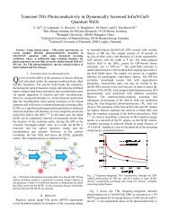
The computational model is shown in Fig. 1 and consists<br />
of the actual computational domain and two additional PML<br />
areas. For this example we consider propagation of an<br />
E-polarized wave governed by<br />
2E 2 n<br />
2<br />
c<br />
E0, 1<br />
FIG. 1. Waveguide with a 90° bend line defect in a periodic configuration of<br />
dielectric columns (n3.4) in air. Unwanted reflections from the input and<br />
output waveguide ports are eliminated by using anisotropic PML regions,<br />
and the energy transmission through the waveguide is evaluated in the unit<br />
cell denoted A.<br />
2022<br />
0003-6951/2004/84(12)/2022/3/$22.00 © 2004 American Institute of Physics<br />
Downloaded 28 Jul 2009 to 192.38.67.112. Redistribution subject to AIP license or copyright; see http://apl.aip.org/apl/copyright.jsp