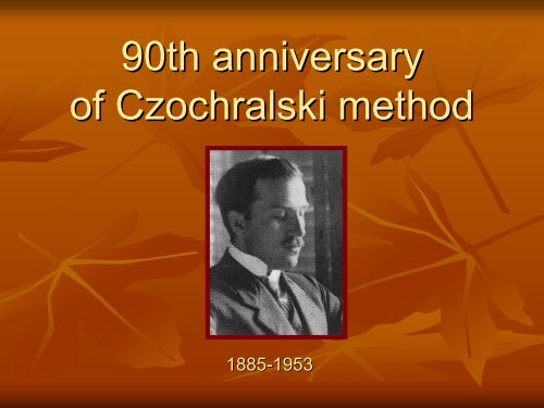
90th anniversary of Czochralski pulling method
90th anniversary of Czochralski pulling method
90th anniversary of Czochralski pulling method

You also want an ePaper? Increase the reach of your titles
YUMPU automatically turns print PDFs into web optimized ePapers that Google loves.
<strong>90th</strong> <strong>anniversary</strong><br />
<strong>of</strong> <strong>Czochralski</strong> <strong>method</strong><br />
1885-1953 1885 1953
In 2006 we celebrate the 90 th <strong>anniversary</strong> <strong>of</strong> <strong>Czochralski</strong> <strong>pulling</strong><br />
<strong>method</strong>.<br />
Pr<strong>of</strong>essor Jan <strong>Czochralski</strong> invented this <strong>method</strong> during the<br />
investigations <strong>of</strong> the crystallization rate <strong>of</strong> metals.<br />
In the fifties <strong>of</strong> the twentieth century his <strong>method</strong> was adopted for<br />
growing large single crystals <strong>of</strong> semiconductors on an industrial<br />
scale.<br />
Moreover, a large group <strong>of</strong> applicable oxides are grown using<br />
<strong>Czochralski</strong> <strong>method</strong>.<br />
Also the number <strong>of</strong> single crystals <strong>of</strong> intermetallic compounds is<br />
quickly growing thanks to this <strong>method</strong>.<br />
The Institute <strong>of</strong> Electronic Materials Technology (ITME)<br />
GdCa 4 O(BO 3 ) 3<br />
UŚ<br />
Fe 2.25 V 0.75 Al
Arms <strong>of</strong> Kcynia<br />
•Pr<strong>of</strong>essor Pr<strong>of</strong>essor Jan <strong>Czochralski</strong> was born on October 23, 1885 in Kcynia, Kcynia,<br />
in<br />
part <strong>of</strong> Poland at that time under the Prussian domination, as the eighth<br />
child <strong>of</strong> the Polish craftsmen Franciszek <strong>Czochralski</strong> and Marta from the<br />
Suchomski family. The <strong>Czochralski</strong>s were carpenters for many<br />
generations.<br />
•Jan Jan completed teachers' seminar in Kcynia according to the wish <strong>of</strong> his<br />
father. He was already interested in chemistry during his school days.<br />
However, he did not accept his matriculation certificate due to poor<br />
grades.<br />
•Lack Lack <strong>of</strong> this certificate unabled him to continue his education. For some<br />
time he worked in Krotoszyn in a drugstore.
Bydgoszcz
Berlin<br />
•At t the end <strong>of</strong> 1904 he went to Berlin and began to work in the drugstore drugstore<br />
<strong>of</strong> Dr. A.<br />
Herbrand in Altglienicke, Altglienicke,<br />
the districts <strong>of</strong> Berlin.<br />
•Later Later he worked for a short period in the laboratory <strong>of</strong> Kunheim and Co. in<br />
Niederschönweide<br />
Niedersch nweide near Berlin and then in Allgemeine Elektrizitäts<br />
Elektrizit ts-Gesellschaft<br />
Gesellschaft<br />
(AEG). The job in Kabelwerk Oberspree and the two years spent in their research<br />
laboratories prepared him to become head <strong>of</strong> the laboratory <strong>of</strong> steel steel<br />
and iron<br />
research. This laboratory dealt with the checking the quality and and<br />
purity <strong>of</strong> metals<br />
and alloys and was engaged in the refinement <strong>of</strong> copper.<br />
•Simultaneously Simultaneously he attended lectures on chemistry at the Charlottenburg<br />
Polytechnic near Berlin.<br />
•From From 1911 to 1914 he was an assistant <strong>of</strong> Wichard von Möllendorff llendorff with whom<br />
he published his first paper devoted to the crystallography <strong>of</strong> metals metals,<br />
, dislocation<br />
theory (Zeitschrift Zeitschrift des Vereines Deutcher Ingenieure<br />
57 (1913) 931-5, 931 5, 1014-20) 1014 20) .<br />
KABELWERK OBERSPREE RESEARCH<br />
LABORATORIES, JAN CZOCHRALSKI (FAR<br />
LEFT).<br />
LEFT)
•Jan Jan <strong>Czochralski</strong> married in 1910 Marguerit Haase, Haase,<br />
a pianist <strong>of</strong> Dutch origin, the<br />
daughter <strong>of</strong> a rich owner <strong>of</strong> houses. They had three children: two daughters –<br />
Leonia (1914) and Cecilia (1920,) and a son Borys (1918).<br />
CZOCHRALSKI'S FAMILY
•In In 1916 pr<strong>of</strong>essor Jan <strong>Czochralski</strong> invented a <strong>method</strong> for measuring the<br />
crystallization velocity <strong>of</strong> metals. The <strong>method</strong> was invented by accident accident<br />
and<br />
through <strong>Czochralski</strong> careful observations.<br />
•The The idea <strong>of</strong> this <strong>method</strong> is based on <strong>pulling</strong> a crystal from the melt. melt.<br />
The grown<br />
during the experiment crystals as metallic wires were single crystals. crystals.<br />
•The The results <strong>of</strong> <strong>Czochralski</strong> studies were published in several papers, The first<br />
one was published in Zeitschrift für Physikalische<br />
hysikalische Chemie 92, 219 (1918), in<br />
German.<br />
•This This new technique allowed to obtain the good<br />
quality single crystals <strong>of</strong> pure metals like Sn, Sn,<br />
Pb, Pb,<br />
Zn.<br />
After the II World War the <strong>Czochralski</strong> <strong>method</strong> was<br />
adopted by the Americans G.K. Teal and J.B. Little<br />
from Bell Telephone Laboratories for growing large<br />
single crystals <strong>of</strong> semiconductors on an industrial<br />
scale (Growth <strong>of</strong> germanium single crystals, Phys.<br />
Rev. 78, 647 (1950) and Bull. Amer. Phys. Soc. 25,<br />
16 (1950)).
Franfurt on Mein<br />
•In In 1917 Jan <strong>Czochralski</strong> moved to Frankfurt on Mein and organized the Laboratory<br />
<strong>of</strong> Metal Science. Science<br />
• Several valuable scientific papers and patents were developed there. there.<br />
Among the<br />
patents was the highly famous patent on a tin-free tin free bearing alloy for railways, called<br />
metal B, patented in 1924 and bought by many countries all over the world, including<br />
USA, France and England.<br />
•He He also pioneered investigations <strong>of</strong> the anisotropy <strong>of</strong> the hardness hardness<br />
<strong>of</strong> single crystals<br />
(works between 1913 and 1923), which are <strong>of</strong> great importance for the plastic<br />
treatment <strong>of</strong> materials.<br />
•In In 1919 <strong>Czochralski</strong> was among the scientists who founded the German Society for<br />
Metal Science and in 1925 he became its presisent. presisent<br />
Warsaw<br />
•When When Poland regained independence he accepted in 1929 the invitation invitation<br />
<strong>of</strong> the<br />
President <strong>of</strong> Poland, Ignacy Mościcki Mo cicki. . <strong>Czochralski</strong> obtained his first honorary<br />
doctorate <strong>of</strong> the Faculty <strong>of</strong> Chemistry at the Warsaw University <strong>of</strong> Technology. Technology.<br />
It<br />
enabled him to take the position <strong>of</strong> a pr<strong>of</strong>essor there.<br />
The <strong>Czochralski</strong>’s<br />
<strong>Czochralski</strong><br />
house in Warsaw
PROF. JAN CZOCHRALSKI, WARSAW, 1929<br />
THE POLISH PRESIDENT IGNACY MOŚCICKI MO CICKI (FAR<br />
RIGHT) VISITING CZOCHRALSKI'S LABORATORY.<br />
JAN CZOCHRALSKI (SECOND FROM THE LEFT). LEFT).
•After After the II World War due to his connections with Germans <strong>Czochralski</strong> <strong>Czochralski</strong><br />
was<br />
suspected <strong>of</strong> collaboration and even arrested. The suspicion was continued to date <strong>of</strong><br />
his dead, but up to now there is no evidence for his collaboration. collaboration.<br />
In fact pr<strong>of</strong>essor<br />
<strong>Czochralski</strong> helped the National Army and many people during the war time.<br />
<strong>Czochralski</strong> returned to Kcynia and to the chemistry and to production production<br />
<strong>of</strong> cosmetics<br />
and household chemicals.<br />
•He He died on April 22, 1953 in Poznań Pozna due to heart disease and was buried in Kcynia.<br />
•Pr<strong>of</strong>essor Pr<strong>of</strong>essor Jan <strong>Czochralski</strong> was outstanding metallurgist, chemist and crystallographer,<br />
whose crystal growth <strong>method</strong> allowed dynamic development <strong>of</strong> the modern modern<br />
science and<br />
technology. However, after the war he was almost forgotten, especially especially<br />
in Poland.<br />
•After After the political changes in Poland the Tenth European Crystallographic Crystallographic<br />
Meeting,<br />
organized in Wroclaw in 1986, was dedicated to Pr<strong>of</strong>essor Jan <strong>Czochralski</strong> to<br />
commemorate the seventieth <strong>anniversary</strong> <strong>of</strong> the discovery <strong>of</strong> the <strong>Czochralski</strong> <strong>method</strong>.<br />
•Since Since its foundation in 1991, the Polish Society for Crystal Growth Growth<br />
commemorates him<br />
in the form <strong>of</strong> <strong>Czochralski</strong> Lecture, which is delivered as the opening lecture <strong>of</strong> every<br />
Polish Crystal Growth Conference by a distinguished scientist with with<br />
recognized<br />
contribution in crystal growth related fields. In 1998 this Society Society<br />
changed its name to<br />
<strong>Czochralski</strong> Polish Society for Crystal Growth.
The <strong>Czochralski</strong>’s<br />
<strong>Czochralski</strong><br />
house in Kcynia<br />
„Margowo Margowo”
Pr<strong>of</strong>essor <strong>Czochralski</strong> started the crystal growth <strong>of</strong> metals by immersion <strong>of</strong> a narrow<br />
capillary in the crucible with melt. In capillary a small nucleus nucleus<br />
<strong>of</strong> crystal was formed.<br />
Slow <strong>pulling</strong> out <strong>of</strong> the melt allowed to obtain metallic monocrystalline wires with<br />
diameters <strong>of</strong> about 1 mm and lengths up to 150 mm. The crystal growth using the<br />
<strong>Czochralski</strong> <strong>method</strong> is continuously improved and developed.<br />
In the Solid State Department <strong>of</strong> the<br />
Institute <strong>of</strong> Physics University <strong>of</strong><br />
Silesia modification <strong>of</strong> the<br />
<strong>Czochralski</strong> <strong>method</strong> from the<br />
levitating melt was applied. Growing<br />
single crystals <strong>of</strong> intermetallics in<br />
crucibles degrades their purity and<br />
quality due contact with the material<br />
<strong>of</strong> the crucible particularly when the<br />
sample contains high reactivity <strong>of</strong><br />
rare earths. The applied crucibleless<br />
<strong>method</strong> allows to obtain a relative<br />
optimal quality <strong>of</strong> single crystals <strong>of</strong><br />
rare earth intermetallics.<br />
intermetallics
RTX intermetallics<br />
Berg-Barrett<br />
Berg Barrett topography<br />
ZrNiAl<br />
TiNiSi
Intensity [a.u.]<br />
20 40 60 80<br />
2θ [deg]<br />
orthorhombic (Dwight)<br />
experimental<br />
hexagonal (Hulliger)
Lattice parameter a [Å]<br />
7.22<br />
7.20<br />
7.18<br />
7.16<br />
7.14<br />
7.12<br />
7.10<br />
GdPdAl<br />
7.08<br />
0 50 100 150 200 250 300<br />
Temperature [K]<br />
Volume [Å 3 ]<br />
182.5<br />
182.0<br />
181.5<br />
181.0<br />
180.5<br />
180.0<br />
GdPdAl<br />
cal (Θ D =260K)<br />
experimental<br />
Lattice parameter c [Å]<br />
4.12<br />
4.10<br />
4.08<br />
4.06<br />
4.04<br />
0 50 100 150 200 250<br />
Temperature [K]<br />
GdPdAl<br />
0 50 100 150 200 250 300<br />
Temperature [K]
The two layers <strong>of</strong> the structure <strong>of</strong><br />
GdPdAl (4 unit cells) at level z=0.5 (a)<br />
and z=0 (b);<br />
only inter-layer bonds are exhibited.<br />
The arrows indicate the movement <strong>of</strong><br />
the Al-atoms and the shortening <strong>of</strong> the<br />
bonds upon cooling (strongly<br />
exaggerated).
Electrical resistivity (µΩm)<br />
30<br />
20<br />
10<br />
T N = 24 K<br />
GdPdAl<br />
T c = 48 K<br />
[105]<br />
180 K<br />
0<br />
0 100 200 300<br />
Temperature (K)
Susceptibility (emu/mole)<br />
12.5<br />
10.0<br />
7.5<br />
5.0<br />
2.5<br />
48 K<br />
θ = 67 K<br />
C = 7.9 emuK/mole<br />
µ eff = 7.94 µ B /f.u.<br />
GdPdAl<br />
H = 360 Oe<br />
10.0<br />
1/χ = (T-θ)/C<br />
0<br />
0 200 400 600 800 1000 0<br />
0 20 40 60 80<br />
7.5<br />
5.0<br />
2.5<br />
Temperature (K)<br />
20 K<br />
48 K<br />
100<br />
80<br />
60<br />
40<br />
20<br />
Inverse susceptibility (mole/emu)
(arb.u.)<br />
'<br />
χ<br />
ac<br />
22 K<br />
48 K<br />
GdPdAl [105]<br />
0 100 200 300<br />
Temperature (K)
Intensity (arb.u.)<br />
VB<br />
Pd 4d<br />
Gd 4f<br />
GdPdAl<br />
GdPdAl<br />
Pd<br />
Gd 5p<br />
0 10 20 30<br />
Binding energy (eV)<br />
0 2<br />
Gd
Intensity (arb. u.)<br />
O rthorhom bic s tructure - Dwight<br />
DyP dAl e xpe rim e nta l<br />
He xa gona l s tructure - Hullige r<br />
10 20 30 40 50 60 70 80 90 100<br />
2θ [de g]<br />
ZrNiAl
Lattice parameter a [Å]<br />
7.18<br />
7.17<br />
7.16<br />
DyPdAl<br />
Cal (Θ D =225K)<br />
Exp<br />
7.15<br />
0 50 100 150 200 250 300<br />
Temperature [K]<br />
Unit cell volume [A 3 ]<br />
177.5<br />
177.0<br />
176.5<br />
176.0<br />
DyPdAl<br />
fit (Θ D =225K)<br />
experimental<br />
Lattice parameter c [Å]<br />
3.985<br />
3.980<br />
3.975<br />
3.970<br />
3.965<br />
3.960<br />
0 50 100 150 200 250 300<br />
Temperature [K]<br />
DyPdAl<br />
Cal (Θ D =225K)<br />
exp<br />
3.955<br />
0 50 100 150 200 250 300<br />
Temperature [K]
Resistivity (µΩm)<br />
0.6<br />
0.5<br />
0.4<br />
0.3<br />
0.2<br />
DyPdAl<br />
17 K<br />
25 K<br />
a axis<br />
0.1<br />
0 100 200<br />
Temperature (K)
Lattice parameter a [A]<br />
7.185<br />
7.180<br />
7.175<br />
7.170<br />
7.165<br />
7.160<br />
HoPdAl<br />
Cal (Θ D =225K)<br />
Exp<br />
7.155<br />
0 50 100 150 200 250 300<br />
Temperature [K]<br />
Volume [A 3 ]<br />
176.0<br />
175.5<br />
175.0<br />
HoPdAl<br />
Cal (Θ D =225K)<br />
Exp<br />
Lattice parameter c [A]<br />
3.950<br />
3.945<br />
3.940<br />
3.935<br />
3.930<br />
3.925<br />
HoPdAl<br />
Cal (Θ D =225K)<br />
Exp<br />
0 50 100 150 200 250 300<br />
Temperature [K]<br />
0 50 100 150 200 250 300<br />
Temperature [K]
Electrical resistivity (µΩm)<br />
2.0<br />
1.5<br />
1.0<br />
0.28<br />
0.21<br />
32 K<br />
GdPdIn<br />
94 K<br />
110 K<br />
90 130<br />
GdPdX<br />
29 K<br />
Sn<br />
0.5<br />
Ge<br />
30 K<br />
18 K<br />
In<br />
0<br />
0<br />
28 K<br />
94 K110<br />
K<br />
100 200 300<br />
Temperature (K)<br />
Al<br />
Si<br />
Ga
Compound<br />
X (IIIA group) group<br />
dρ ph /dT(µΩcm/K)<br />
0.6<br />
0.4<br />
0.2<br />
Al<br />
Si<br />
Crystal<br />
structure<br />
V (Å ( 3 )<br />
GdPdAl (143pm) TiNiSi<br />
240.4<br />
GdPdGa (135pm) Co 2 Si<br />
240.3<br />
GdPdIn (167pm) Co 2 Si<br />
223.0<br />
Ga<br />
Ge<br />
Sn<br />
y=Bexp(-d)<br />
B=83<br />
0<br />
4.5 5.0 5.5 6.0 6.5 7.0<br />
d<br />
Pd 4d<br />
ΓFWHM FWHM (eV eV)<br />
In<br />
Compound<br />
X (IVA group) group<br />
Crystal<br />
structure<br />
V (Å ( 3 )<br />
2.2 GdPdSi (118 pm) pm β – GdPdSi<br />
455.0<br />
1.7 GdPdGe (122 pm) pm β – GdPdGe<br />
471.6<br />
1.3 GdPdSn (140 pm) pm Co 2 Si<br />
264.9<br />
d = M·n/V<br />
Pd 4d<br />
ΓFWHM FWHM<br />
2.4<br />
2.1<br />
1.9<br />
(M – molecular mass <strong>of</strong> the<br />
GdPdX compound,<br />
n – number <strong>of</strong> molecules per<br />
unit cell volume,<br />
V- unit cell volume)<br />
(eV eV)
Intensity (arb.u.)<br />
Pd 4d<br />
Gd 4f<br />
Gd 5p<br />
GdPdSi<br />
GdPdIn<br />
0 10 20 30<br />
Binding energy (eV)
Gd 7T3 Berg-Barrett topography <strong>of</strong> the Gd 7Pd 3 single crystal<br />
Th 7 Fe 3
Berg-Barrett topography <strong>of</strong> the Gd 7Pd 3 single crystal
Berg-Barrett topography <strong>of</strong> the Gd 7Rh 3 single crystal
Intensity (arb.u.)<br />
Intensity (arb.u.)<br />
210<br />
210<br />
002<br />
102<br />
211<br />
112<br />
301<br />
202<br />
220<br />
212<br />
311<br />
400<br />
302<br />
401<br />
411<br />
402<br />
322<br />
303<br />
500<br />
e x p<br />
c a l<br />
30 40 50 60<br />
002<br />
102<br />
211<br />
300<br />
301<br />
112<br />
202<br />
220<br />
212<br />
Gd 7Rh Rh3 2 θ (d e g )<br />
Gd 7Pd Pd3 311<br />
400<br />
302<br />
401<br />
3 0 4 0 5 0 6 0<br />
2 θ (d e g )<br />
321<br />
410<br />
410<br />
411<br />
402<br />
213<br />
213<br />
500<br />
303<br />
322<br />
330<br />
330<br />
412<br />
412<br />
e x p<br />
c a l<br />
421<br />
004<br />
313<br />
004<br />
104
Lattice parameter a (Å)<br />
Lattice parameter c (Å)<br />
Volume (Å 3 )<br />
9.86<br />
9.85<br />
9.84<br />
9.83<br />
9.82<br />
6.212<br />
6.208<br />
6.204<br />
6.200<br />
6.196<br />
6.192<br />
523<br />
522<br />
521<br />
520<br />
519<br />
518<br />
Gd 7 Rh 3<br />
T N<br />
0 50 100 150 200 250 300<br />
0 50 100 150 200 250 300<br />
0 50 100 150 200 250 300<br />
Temperature (K)<br />
exp<br />
cal (Θ D =160K)<br />
b)<br />
c)<br />
a)<br />
Lattice parameter a (Å)<br />
Lattice parameter c (Å)<br />
Volume (Å 3 )<br />
9.985 T c<br />
9.980<br />
9.975<br />
9.970<br />
9.965<br />
9.960<br />
9.955<br />
6.285<br />
6.280<br />
6.275<br />
6.270<br />
6.265<br />
6.260<br />
543<br />
542<br />
541<br />
540<br />
539<br />
538<br />
Gd 7 Pd 3<br />
0 50 100 150 200 250 300 350 400<br />
0 50 100 150 200 250 300 350 400<br />
0 50 100 150 200 250 300 350 400<br />
Temperature (K)<br />
exp<br />
cal (Θ D =160K)<br />
a)<br />
b)<br />
c)
Intensity (arb.u.)<br />
Gd 5d<br />
Pd 4d<br />
Rh 4d<br />
Gd 7 Rh 3<br />
Gd 7 Pd 3<br />
Gd<br />
Gd 4f<br />
Gd 5p<br />
0 10 20 30<br />
Binding energy (eV)<br />
-1 0 1 2 3 4
ρ (µΩcm)<br />
200<br />
150<br />
100<br />
50<br />
Gd 7 Rh 3<br />
T N = 140 K<br />
ρ(T)=130+0.022T 2<br />
ρ(T)=27+0.005T 2<br />
i // c<br />
i // a<br />
0 100 200 300<br />
T (K)<br />
ρ (µΩcm)<br />
250<br />
200<br />
150<br />
100<br />
50<br />
Gd 7 Pd 3<br />
ρ(T)=60+0.022T 2<br />
ρ(T)=27+0.015T 2<br />
0 100 200 300 400<br />
T (K)<br />
T 2<br />
T=332 K<br />
i II a<br />
i II c
S (µV/K)<br />
S (µV/K)<br />
12<br />
10<br />
8<br />
6<br />
4<br />
2<br />
0<br />
-2<br />
-4<br />
-6<br />
-8<br />
0 50 100 150 200 250 300<br />
12<br />
10<br />
8<br />
6<br />
4<br />
2<br />
0<br />
∆T II c<br />
∆T II a<br />
∆T II a<br />
∆T II c<br />
T N<br />
T (K)<br />
Gd 7 Pd 3<br />
-2<br />
0 50 100 150 200 250 300 350<br />
T(K)<br />
Gd 7 Rh 3<br />
a)<br />
b)<br />
T c
ρ (µΩcm)<br />
ρ (µΩcm)<br />
80<br />
60<br />
40<br />
20<br />
200<br />
160<br />
120<br />
80<br />
Gd 7 Rh 3<br />
i // c<br />
i // a<br />
B = 0 T<br />
B = 8 T<br />
140 K<br />
40<br />
0 50 100 150 200<br />
T (K)<br />
B = 0 T<br />
B = 8 T<br />
ρ (µΩcm)<br />
ρ (µΩcm)<br />
250<br />
200<br />
150<br />
100<br />
110<br />
90<br />
70<br />
50<br />
Gd 7 Pd 3<br />
B = 0 T<br />
B = 0 T<br />
B = 8T<br />
B = 8T<br />
i II a<br />
i II c<br />
30<br />
0 100 200 300<br />
T (K)
M (µ B /Gd)<br />
M (µ B /Gd)<br />
0.0003<br />
0.0002<br />
0.0001<br />
0.015<br />
0.010<br />
0.005<br />
II c<br />
II a<br />
0<br />
0 100 200 300 400<br />
II a<br />
II c<br />
T N =140 K<br />
Gd 7 Pd 3<br />
B = 0.1 T<br />
T C =334 K<br />
0<br />
0 100 200 300 400<br />
T (K)<br />
Gd Rh<br />
7 3<br />
B = 0.5 T<br />
ZFC<br />
a)<br />
b)<br />
Susceptibility (emu/mole)<br />
Susceptibility (emu/mole)<br />
1.5<br />
1.0<br />
0.5<br />
0<br />
0<br />
80<br />
300 600 900<br />
Gd Pd<br />
7 3<br />
B = 0.03 T<br />
B II a<br />
0<br />
60<br />
40<br />
20<br />
T N =140 K<br />
Gd 7 Rh 3<br />
χ -1 =(T-176)/58.4<br />
µ eff =8.2µ B<br />
χ -1 =(T-355)/56.5<br />
µ eff = 8.0 µ B<br />
325 K<br />
T c =332 K<br />
0<br />
0 200 400 600<br />
Temperature (K)<br />
B = 0.19 T<br />
B II a<br />
12<br />
8<br />
4<br />
4<br />
2<br />
0<br />
Inverse susceptibility (mole/emu)<br />
Inverse susceptibility (mole/emu)
GdPdAl(I) GdPdAl(I)<br />
0.56<br />
c/a a/a a/ Gd<br />
c/c c/ Gd<br />
V/V V/ Gd<br />
GdPdAl(II) GdPdAl(II)<br />
0.57<br />
1.96 0.71 2.75<br />
Gd 7 Rh Rh3 Gd 7 Pd Pd3 µ<br />
eff<br />
=<br />
g<br />
J<br />
µ<br />
gJ – the Lande factor<br />
0.63<br />
0.63<br />
B<br />
J<br />
J – the total quantum number<br />
N(E F) ) – the desity <strong>of</strong> states at the Fermi energy<br />
A – the exchange interaction<br />
2 0.7 2.78<br />
2.72 72 1.09 2.65<br />
2.75 1.09 2.75<br />
⎡ g −1⎤<br />
( ) ( ) J<br />
J + 1 ⎢1<br />
+ AN EF<br />
⎥<br />
⎣<br />
g J ⎦
Acknowledgments<br />
Author thanks <strong>Czochralski</strong> Polish Society for Crystal Growth for source<br />
materials (http://www.<br />
( http://www.ptwk ptwk.org.pl/eng/sitemap.html<br />
.org.pl/eng/sitemap.html)<br />
Paweł Pawe Tomaszewski „Jan Jan <strong>Czochralski</strong> and his <strong>method</strong>” <strong>method</strong> 2003<br />
Cooperation:<br />
Cooperation<br />
M. Klimczak, J. Kusz, R. Troć, Tro , A. Winiarski,<br />
M. Skutecka