Experiments with Bose-Einstein Condensation in an Optical Box
Experiments with Bose-Einstein Condensation in an Optical Box
Experiments with Bose-Einstein Condensation in an Optical Box

You also want an ePaper? Increase the reach of your titles
YUMPU automatically turns print PDFs into web optimized ePapers that Google loves.
Copyright<br />
by<br />
Todd Philip Meyrath<br />
2005
The Dissertation Committee for Todd Philip Meyrath<br />
certifies that this is the approved version of the follow<strong>in</strong>g dissertation:<br />
<strong>Experiments</strong> <strong>with</strong> <strong>Bose</strong>-<strong>E<strong>in</strong>ste<strong>in</strong></strong> <strong>Condensation</strong> <strong>in</strong> <strong>an</strong><br />
<strong>Optical</strong> <strong>Box</strong><br />
Committee:<br />
Mark G. Raizen, Supervisor<br />
Michael F. Becker<br />
M<strong>an</strong>fred F<strong>in</strong>k<br />
Lothar W. Frommhold<br />
Greg O. Sitz
<strong>Experiments</strong> <strong>with</strong> <strong>Bose</strong>-<strong>E<strong>in</strong>ste<strong>in</strong></strong> <strong>Condensation</strong> <strong>in</strong> <strong>an</strong><br />
<strong>Optical</strong> <strong>Box</strong><br />
by<br />
Todd Philip Meyrath, B.S.;B.S.;M.S.;M.S.<br />
DISSERTATION<br />
Presented to the Faculty of the Graduate School of<br />
The University of Texas at Aust<strong>in</strong><br />
<strong>in</strong> Partial Fulfillment<br />
of the Requirements<br />
for the Degree of<br />
DOCTOR OF PHILOSOPHY<br />
THE UNIVERSITY OF TEXAS AT AUSTIN<br />
May 2005
To my parents, Fr<strong>an</strong>k <strong>an</strong>d Donna Meyrath,<br />
for so m<strong>an</strong>y years of love <strong>an</strong>d support,<br />
<strong>with</strong>out which I would have never made it this far.
Acknowledgments<br />
I would like to th<strong>an</strong>k Professor Mark Raizen who has been my advisor<br />
dur<strong>in</strong>g these years. Mark has been <strong>an</strong> endless source of ideas <strong>an</strong>d directions for<br />
<strong>in</strong>terest<strong>in</strong>g experiments. He is <strong>an</strong> outst<strong>an</strong>d<strong>in</strong>g physicist <strong>an</strong>d genu<strong>in</strong>e <strong>in</strong>dividual.<br />
Work<strong>in</strong>g <strong>in</strong> Mark’s laboratory has been <strong>an</strong> excellent <strong>an</strong>d unique privilege.<br />
Dur<strong>in</strong>g my years at UT, I have <strong>in</strong>teracted <strong>with</strong> quite a number of peo-<br />
ple. In recent years I have worked <strong>with</strong> Jay H<strong>an</strong>ssen, Flori<strong>an</strong> Schreck, <strong>an</strong>d<br />
Chih-sung Chuu on the projects presented here. I’ve known Jay s<strong>in</strong>ce the<br />
beg<strong>in</strong>n<strong>in</strong>g of graduate school, we had m<strong>an</strong>y of our classes together as well as<br />
be<strong>in</strong>g work partners <strong>in</strong> the lab for m<strong>an</strong>y projects. In addition to be<strong>in</strong>g a very<br />
talented physicist, Jay is one of the best karaoke s<strong>in</strong>gers I have ever seen (not<br />
heard). Jay <strong>an</strong>d I enjoyed the pa<strong>in</strong> <strong>an</strong>d thrill of learn<strong>in</strong>g to make a BEC from<br />
scratch <strong>an</strong>d a multitude of barbecue runs. Flori<strong>an</strong> was our postdoc. He al-<br />
ways amazed me <strong>with</strong> his limitless drive <strong>an</strong>d determ<strong>in</strong>ation. He is a first class<br />
experimentalist — whom I expect will be a big star the physics community.<br />
No matter what was happen<strong>in</strong>g or how problematic a system could become,<br />
he had <strong>an</strong> idea. See<strong>in</strong>g Flori<strong>an</strong> program was like watch<strong>in</strong>g <strong>an</strong> action movie.<br />
He is also a pretty me<strong>an</strong> <strong>in</strong>-l<strong>in</strong>e skater, <strong>an</strong>d I have the wounds to prove it.<br />
Chih-sung jo<strong>in</strong>ed our experiment sometime shortly after our BEC apparatus<br />
was started. Chih-sung is <strong>an</strong> extremely smart if not very audible guy <strong>an</strong>d is<br />
v
as dedicated to the experiment as he is to his beloved homel<strong>an</strong>d. He has <strong>an</strong><br />
excellent underst<strong>an</strong>d<strong>in</strong>g of physics <strong>an</strong>d experimental work. Our experiment<br />
was jo<strong>in</strong>ed recently by Gabriel Price. Off to a good start, he <strong>an</strong>d Chih-sung<br />
will take the experiment to the next stages <strong>in</strong> the future.<br />
On the sodium experiment, Braulio Guttiérez has lead a mammoth<br />
project, narrowly loos<strong>in</strong>g to us the race for the BEC <strong>in</strong> our lab. Of course, he<br />
knows that the deck was stacked <strong>with</strong> rubidium. I’ve known Braulio all of my<br />
graduate career. He is <strong>an</strong> outst<strong>an</strong>d<strong>in</strong>g physicist <strong>with</strong> a detailed underst<strong>an</strong>d<strong>in</strong>g<br />
of science <strong>an</strong>d also a m<strong>an</strong> of broad <strong>in</strong>terest. The memory of our year as senior<br />
lab TAs will l<strong>in</strong>ger on forever. Kev<strong>in</strong> Henderson is a tremendously hardwork<strong>in</strong>g<br />
scientist <strong>an</strong>d a bright <strong>an</strong>d <strong>in</strong>tuitive experimentalist. Another m<strong>an</strong> of broad<br />
<strong>in</strong>terests, he was always <strong>an</strong> <strong>in</strong>terest<strong>in</strong>g one <strong>with</strong> whom to converse. His tales<br />
are always fasc<strong>in</strong>at<strong>in</strong>g to hear. Hrishikesh Kelkar is a very talented <strong>in</strong>dividual<br />
<strong>with</strong> a strong grasp of physics <strong>an</strong>d the elbow grease to go <strong>with</strong> it. He is also a<br />
me<strong>an</strong> bowler. The sodium experiment was recently jo<strong>in</strong>ed by Tongc<strong>an</strong>g Li, I<br />
c<strong>an</strong>’t say that I know him well yet, but I am confident he will have <strong>an</strong> enjoyable<br />
time <strong>in</strong> the lab that has treated me so well.<br />
Artëm Dudarev <strong>an</strong>d Chu<strong>an</strong>wei Zh<strong>an</strong>g have done amaz<strong>in</strong>g theoretical<br />
work that has supported our experimental thrust. Artëm is <strong>an</strong> extremely<br />
talented physicist <strong>with</strong> a vast knowledge of <strong>in</strong>terest<strong>in</strong>g physics. He has also<br />
shared <strong>an</strong> apartment <strong>with</strong> me for some years <strong>an</strong>d has always been <strong>an</strong> <strong>in</strong>terest<strong>in</strong>g<br />
one <strong>with</strong> whom to converse. He brought to me <strong>an</strong> <strong>in</strong>terest <strong>in</strong> eastern Europe<strong>an</strong><br />
l<strong>an</strong>guage <strong>an</strong>d culture. Chu<strong>an</strong>wei has a most impressive underst<strong>an</strong>d<strong>in</strong>g physics<br />
vi
<strong>an</strong>d a keen ability to solve problems.<br />
To everyth<strong>in</strong>g, there is a beg<strong>in</strong>n<strong>in</strong>g. When I arrived, there were already<br />
senior students Mart<strong>in</strong> Fischer, D<strong>an</strong>iel Steck, <strong>an</strong>d W<strong>in</strong>dell Oskay as well as<br />
postdoc Valery Milner. When I first walked through the doors I was stunned<br />
by the knowledge <strong>an</strong>d experience of these <strong>in</strong>dividuals. I was fortunate enough<br />
to spend time <strong>with</strong> each of them. As I worked on projects <strong>in</strong> the first years,<br />
it was most helpful to have their various op<strong>in</strong>ions <strong>an</strong>d ideas which seemed<br />
limitless.<br />
I had the unique opportunity to <strong>in</strong>teract <strong>with</strong> Kirk Madison. A physi-<br />
cist who graduated from our lab before my time, but came back to UT as a<br />
postdoc <strong>in</strong> the high energy laser group. Discussions that Jay <strong>an</strong>d I had <strong>with</strong><br />
Kirk laid much of the ground work for this experiment. Kirk <strong>an</strong>d I had m<strong>an</strong>y<br />
<strong>in</strong>terest<strong>in</strong>g conversations especially about the m<strong>an</strong>y technical issues of build<strong>in</strong>g<br />
a BEC apparatus.<br />
Outside of the lab, the department has provided us <strong>with</strong> the unpar-<br />
alleled support of a world-class mach<strong>in</strong>e shop run by Allen Schroeder. He is<br />
<strong>an</strong> amaz<strong>in</strong>g mach<strong>in</strong>ist <strong>an</strong>d <strong>an</strong> outst<strong>an</strong>d<strong>in</strong>g coord<strong>in</strong>ator of the mach<strong>in</strong>e shop<br />
effort. His team never failed to dazzle me <strong>with</strong> their skill <strong>an</strong>d speed. Allen<br />
has a keen ability to get the jobs done right <strong>an</strong>d never failed to rapidly re-<br />
spond to our m<strong>an</strong>y emergency situations. Jack Clifford has run the student<br />
mach<strong>in</strong>e shop all my time at UT. In addition to be<strong>in</strong>g <strong>an</strong> extremely friendly<br />
<strong>in</strong>dividual, he has a keen skill <strong>with</strong> the mach<strong>in</strong>es <strong>an</strong>d taught me all I know<br />
about mach<strong>in</strong><strong>in</strong>g. L<strong>an</strong>ny S<strong>an</strong>defur <strong>an</strong>d Ed Baez have been excellent support<br />
vii
<strong>in</strong> the cryogenics shop. The Center for Nonl<strong>in</strong>ear Dynamics adm<strong>in</strong>istrative<br />
staff Olga Vera, Rosie Tovar, <strong>an</strong>d Elena Simmons made sure our orders went<br />
though <strong>an</strong>d made all the paper work go smoothly. They also provided their<br />
friendly smiles <strong>an</strong>d k<strong>in</strong>d words.<br />
Th<strong>an</strong>ks would not be complete <strong>with</strong>out mention<strong>in</strong>g mention<strong>in</strong>g my be-<br />
g<strong>in</strong>n<strong>in</strong>g <strong>in</strong> laboratory work as <strong>an</strong> undergraduate <strong>in</strong> Mike Schatz’s lab at Geor-<br />
gia Tech. Prof. Schatz <strong>in</strong>troduced me to the excit<strong>in</strong>g world of experimental<br />
physics. Summer 1997, which I spent as <strong>an</strong> undergraduate researcher at Los<br />
Alamos, was also <strong>an</strong> outst<strong>an</strong>d<strong>in</strong>g learn<strong>in</strong>g experience. I th<strong>an</strong>k D<strong>an</strong>iel James<br />
for his encouragement to pursue graduate studies <strong>in</strong> physics. I am grateful to<br />
my committee who has taken the time to read this dissertation <strong>an</strong>d who have<br />
provided guid<strong>an</strong>ce <strong>an</strong>d <strong>in</strong>spiration over the years.<br />
I appreciate the comments <strong>an</strong>d corrections of Jay H<strong>an</strong>ssen <strong>an</strong>d Artëm<br />
Dudarev. I would also like to acknowledge Jay H<strong>an</strong>ssen who helped <strong>with</strong><br />
the writ<strong>in</strong>g of several sections describ<strong>in</strong>g the experimental systems that he<br />
designed <strong>an</strong>d built <strong>an</strong>d the dissertation figures that we have shared.<br />
I also must th<strong>an</strong>k the National Science Foundation for three years of<br />
support through the NSF Graduate Research Fellowship.<br />
viii<br />
T.P.M.<br />
Aust<strong>in</strong>, Texas<br />
April 2005
<strong>Experiments</strong> <strong>with</strong> <strong>Bose</strong>-<strong>E<strong>in</strong>ste<strong>in</strong></strong> <strong>Condensation</strong> <strong>in</strong> <strong>an</strong><br />
Publication No.<br />
<strong>Optical</strong> <strong>Box</strong><br />
Todd Philip Meyrath, Ph.D.<br />
The University of Texas at Aust<strong>in</strong>, 2005<br />
Supervisor: Mark G. Raizen<br />
This dissertation details the experimental methods used to produce a<br />
<strong>Bose</strong>-<strong>E<strong>in</strong>ste<strong>in</strong></strong> condensate (BEC) <strong>in</strong> <strong>an</strong> optical box trap. This novel optical<br />
trap type has strong conf<strong>in</strong>ement <strong>in</strong> two directions comparable to that which<br />
is possible <strong>in</strong> <strong>an</strong> optical lattice, yet produces <strong>in</strong>dividually addressable conden-<br />
sates. The optical trap is based on <strong>an</strong> pair of elongated Hermite-Gaussi<strong>an</strong><br />
TEM01 mode beams <strong>an</strong>d tailored by designer box wall beams. Us<strong>in</strong>g this<br />
method, we have succeeded <strong>in</strong> produc<strong>in</strong>g <strong>in</strong>dividual highly conf<strong>in</strong>ed lower di-<br />
mensional condensates. The box trap is <strong>in</strong>tegrated <strong>with</strong> s<strong>in</strong>gle atom detection<br />
capability, pav<strong>in</strong>g the way for studies of qu<strong>an</strong>tum atom statistics.<br />
ix
Table of Contents<br />
Acknowledgments v<br />
Abstract ix<br />
List of Tables xvi<br />
List of Figures xvii<br />
Chapter 1. Overview 1<br />
1.1 Units <strong>an</strong>d Orders of Magnitude . . . . . . . . . . . . . . . . . 1<br />
1.2 <strong>Bose</strong>-<strong>E<strong>in</strong>ste<strong>in</strong></strong> <strong>Condensation</strong> . . . . . . . . . . . . . . . . . . . 2<br />
1.3 Why MOTs, Magnetic Traps, <strong>an</strong>d <strong>Optical</strong> Traps? . . . . . . . 3<br />
1.4 Why a S<strong>in</strong>gle High Frequency <strong>Optical</strong> Trap? . . . . . . . . . . 4<br />
1.5 Chapter Overview . . . . . . . . . . . . . . . . . . . . . . . . . 5<br />
Chapter 2. Operational Concepts 7<br />
2.1 Light Forces on Atoms . . . . . . . . . . . . . . . . . . . . . . 7<br />
2.2 Magneto-<strong>Optical</strong> Trapp<strong>in</strong>g . . . . . . . . . . . . . . . . . . . . 9<br />
2.2.1 <strong>Optical</strong> Molasses <strong>in</strong> 1-D . . . . . . . . . . . . . . . . . . 9<br />
2.2.2 1D-MOT . . . . . . . . . . . . . . . . . . . . . . . . . . 10<br />
2.3 Magnetic Trapp<strong>in</strong>g . . . . . . . . . . . . . . . . . . . . . . . . 13<br />
2.4 <strong>Optical</strong> Trapp<strong>in</strong>g . . . . . . . . . . . . . . . . . . . . . . . . . 14<br />
2.5 Absorptive Imag<strong>in</strong>g . . . . . . . . . . . . . . . . . . . . . . . . 15<br />
Chapter 3. Experimental Apparatus 17<br />
3.1 Introduction . . . . . . . . . . . . . . . . . . . . . . . . . . . . 17<br />
3.2 Vacuum Chamber . . . . . . . . . . . . . . . . . . . . . . . . . 19<br />
3.2.1 Upper Chamber . . . . . . . . . . . . . . . . . . . . . . 19<br />
3.2.2 Lower Chamber . . . . . . . . . . . . . . . . . . . . . . 22<br />
x
3.2.2.1 Pump<strong>in</strong>g Region . . . . . . . . . . . . . . . . . 23<br />
3.2.2.2 Science Chamber Region . . . . . . . . . . . . 25<br />
3.3 The Near Reson<strong>an</strong>ce Lasers . . . . . . . . . . . . . . . . . . . 29<br />
3.3.1 The Grat<strong>in</strong>g Stabilized Lasers . . . . . . . . . . . . . . . 31<br />
3.3.1.1 The MOT Master Laser . . . . . . . . . . . . . 34<br />
3.3.1.2 The Repump Laser . . . . . . . . . . . . . . . . 36<br />
3.3.2 Injection Locked MOT Lasers . . . . . . . . . . . . . . 38<br />
3.3.2.1 Upper MOT Horizontal Slave Laser . . . . . . 40<br />
3.3.2.2 Upper MOT Diagonal Slave Laser . . . . . . . 42<br />
3.3.2.3 Lower MOT Slave Laser . . . . . . . . . . . . . 44<br />
3.4 The Far-Off Reson<strong>an</strong>ce Lasers . . . . . . . . . . . . . . . . . . 44<br />
3.5 The Magnetic Trap . . . . . . . . . . . . . . . . . . . . . . . . 46<br />
3.5.1 Quadrupole Ioffe Configuration . . . . . . . . . . . . . . 47<br />
3.5.2 Experimental Characterization . . . . . . . . . . . . . . 50<br />
3.5.3 Decompressed Ioffe Configuration . . . . . . . . . . . . 52<br />
3.5.4 Auxiliary Coils . . . . . . . . . . . . . . . . . . . . . . 57<br />
3.5.5 Coil Structure <strong>an</strong>d Construction . . . . . . . . . . . . . 58<br />
3.5.6 Current Control . . . . . . . . . . . . . . . . . . . . . . 65<br />
3.6 Computer Control . . . . . . . . . . . . . . . . . . . . . . . . . 69<br />
3.7 Experimental Sequence . . . . . . . . . . . . . . . . . . . . . . 70<br />
3.7.1 Upper MOT . . . . . . . . . . . . . . . . . . . . . . . . 70<br />
3.7.2 Lower MOT . . . . . . . . . . . . . . . . . . . . . . . . 72<br />
3.7.3 <strong>Optical</strong> Pump<strong>in</strong>g <strong>an</strong>d Magnetic Trap Load<strong>in</strong>g . . . . . 75<br />
3.7.4 Evaporative Cool<strong>in</strong>g . . . . . . . . . . . . . . . . . . . . 79<br />
3.7.5 The Signature of <strong>Condensation</strong> . . . . . . . . . . . . . . 84<br />
3.8 Imag<strong>in</strong>g of Atoms . . . . . . . . . . . . . . . . . . . . . . . . . 86<br />
3.8.1 Absorption Imag<strong>in</strong>g . . . . . . . . . . . . . . . . . . . . 86<br />
3.8.2 Florescence Imag<strong>in</strong>g . . . . . . . . . . . . . . . . . . . . 90<br />
3.8.3 Atom Count<strong>in</strong>g . . . . . . . . . . . . . . . . . . . . . . 90<br />
xi
Chapter 4. Lower Dimensional BEC 98<br />
4.1 <strong>Bose</strong>-<strong>E<strong>in</strong>ste<strong>in</strong></strong> Statistics . . . . . . . . . . . . . . . . . . . . . . 98<br />
4.2 Weakly Interact<strong>in</strong>g Gas . . . . . . . . . . . . . . . . . . . . . . 100<br />
4.3 Three-Dimensional Condensates . . . . . . . . . . . . . . . . . 102<br />
4.4 Two-Dimensional Condensates . . . . . . . . . . . . . . . . . 104<br />
4.5 One-Dimensional Condensates . . . . . . . . . . . . . . . . . . 106<br />
Chapter 5. <strong>Bose</strong>-<strong>E<strong>in</strong>ste<strong>in</strong></strong> Condensate <strong>in</strong> <strong>an</strong> <strong>Optical</strong> <strong>Box</strong> 109<br />
5.1 Introduction . . . . . . . . . . . . . . . . . . . . . . . . . . . . 109<br />
5.2 Beam Overview . . . . . . . . . . . . . . . . . . . . . . . . . . 110<br />
5.3 Other <strong>Optical</strong> Traps . . . . . . . . . . . . . . . . . . . . . . . . 115<br />
5.3.1 Gravito-optical Trap . . . . . . . . . . . . . . . . . . . . 115<br />
5.3.2 Compressed Gaussi<strong>an</strong> Sheets <strong>Optical</strong> Trap . . . . . . . 118<br />
5.4 Hermite-Gaussi<strong>an</strong> TEM01 Trap . . . . . . . . . . . . . . . . . . 120<br />
5.5 Hermite-Gaussi<strong>an</strong> Beam Production . . . . . . . . . . . . . . . 123<br />
5.6 <strong>Optical</strong> Trap Beam Layout . . . . . . . . . . . . . . . . . . . 126<br />
5.7 Beam Multiplex<strong>in</strong>g . . . . . . . . . . . . . . . . . . . . . . . . 130<br />
5.8 Load<strong>in</strong>g Sequence for the <strong>Optical</strong> Trap . . . . . . . . . . . . . 132<br />
5.9 Two-Dimensional BEC <strong>in</strong> hTEM01 Trap . . . . . . . . . . . . 136<br />
5.10 <strong>Box</strong> Wall Beams . . . . . . . . . . . . . . . . . . . . . . . . . 138<br />
5.11 Compensation Beam . . . . . . . . . . . . . . . . . . . . . . . 139<br />
5.12 <strong>Bose</strong>-<strong>E<strong>in</strong>ste<strong>in</strong></strong> Condensate <strong>in</strong> a <strong>Box</strong> . . . . . . . . . . . . . . . 140<br />
5.13 Comments on the <strong>Optical</strong> Trap . . . . . . . . . . . . . . . . . 144<br />
Chapter 6. A Qu<strong>an</strong>tum Tweezer for Atoms 148<br />
6.1 The Qu<strong>an</strong>tum Tweezer Concept . . . . . . . . . . . . . . . . . 148<br />
6.2 Qu<strong>an</strong>tum Tweezer Theory . . . . . . . . . . . . . . . . . . . . 150<br />
6.3 Experimental Possibilities . . . . . . . . . . . . . . . . . . . . 156<br />
6.4 Count<strong>in</strong>g Atoms <strong>in</strong> the <strong>Optical</strong> Trap . . . . . . . . . . . . . . 158<br />
6.5 Future Outlook . . . . . . . . . . . . . . . . . . . . . . . . . . 163<br />
Appendices 164<br />
xii
Appendix A. Magnetic Coils 165<br />
A.1 Some Theory of Electromagnets . . . . . . . . . . . . . . . . . 165<br />
A.1.1 Exact Field of a Circular Current Loop . . . . . . . . . 165<br />
A.1.2 Approximations for Circular Current Loops . . . . . . . 167<br />
A.1.3 Circular Coil Pairs . . . . . . . . . . . . . . . . . . . . . 167<br />
A.1.4 Exact Field of a Square Current Loop . . . . . . . . . . 169<br />
A.1.5 Approximations for Square Current Loops . . . . . . . . 171<br />
A.1.6 Square Coil Pairs . . . . . . . . . . . . . . . . . . . . . . 172<br />
A.2 Numerical Calculations of Fields . . . . . . . . . . . . . . . . . 174<br />
A.3 Power <strong>an</strong>d Cool<strong>in</strong>g . . . . . . . . . . . . . . . . . . . . . . . . 175<br />
A.3.1 Power <strong>in</strong>to a Coil . . . . . . . . . . . . . . . . . . . . . . 175<br />
A.3.2 Water Cool<strong>in</strong>g . . . . . . . . . . . . . . . . . . . . . . . 176<br />
A.3.3 Stability of a Magnetic Trap . . . . . . . . . . . . . . . 177<br />
A.4 Some St<strong>an</strong>dard Americ<strong>an</strong> Wire Types . . . . . . . . . . . . . . 178<br />
A.5 Induct<strong>an</strong>ce <strong>an</strong>d Switch<strong>in</strong>g . . . . . . . . . . . . . . . . . . . . . 179<br />
A.5.1 Induct<strong>an</strong>ce <strong>an</strong>d Parasitics . . . . . . . . . . . . . . . . . 179<br />
A.5.2 Switch<strong>in</strong>g . . . . . . . . . . . . . . . . . . . . . . . . . . 181<br />
A.5.3 Comment on Steel Chambers . . . . . . . . . . . . . . . 183<br />
Appendix B. Magnetic Trap Schematics <strong>an</strong>d Photos 184<br />
Appendix C. Analog Control Electronics 191<br />
C.1 Multipurpose PID Controller . . . . . . . . . . . . . . . . . . 191<br />
C.2 Current Controller for Laser Diodes . . . . . . . . . . . . . . . 198<br />
C.3 Laser Intensity Stabilization . . . . . . . . . . . . . . . . . . . 198<br />
C.4 Uni- <strong>an</strong>d Bi-directional Current Output Stages . . . . . . . . 201<br />
C.5 Ma<strong>in</strong> Power Output Stage for QUIC Trap . . . . . . . . . . . 205<br />
C.6 Shunt Power Circuit for QUIC Trap Coils . . . . . . . . . . . 207<br />
C.7 Analog Optocouplers . . . . . . . . . . . . . . . . . . . . . . . 210<br />
xiii
Appendix D. Computer Control System Hardware 213<br />
D.1 Digital Bus System . . . . . . . . . . . . . . . . . . . . . . . . 213<br />
D.1.1 Overview . . . . . . . . . . . . . . . . . . . . . . . . . . 213<br />
D.1.2 Concept . . . . . . . . . . . . . . . . . . . . . . . . . . . 218<br />
D.1.3 Why a Strobe? . . . . . . . . . . . . . . . . . . . . . . . 218<br />
D.1.4 Flat Ribbon Connection Diagram . . . . . . . . . . . . . 219<br />
D.1.5 Computer Output . . . . . . . . . . . . . . . . . . . . . 221<br />
D.2 Digital Output Boards . . . . . . . . . . . . . . . . . . . . . . 221<br />
D.2.1 Features . . . . . . . . . . . . . . . . . . . . . . . . . . . 222<br />
D.2.2 The Pr<strong>in</strong>ted Circuit Board . . . . . . . . . . . . . . . . 223<br />
D.2.3 Circuit Theory . . . . . . . . . . . . . . . . . . . . . . . 223<br />
D.3 Analog Output Boards . . . . . . . . . . . . . . . . . . . . . . 226<br />
D.3.1 Features . . . . . . . . . . . . . . . . . . . . . . . . . . . 227<br />
D.3.2 Adv<strong>an</strong>tages <strong>an</strong>d Disadv<strong>an</strong>tages . . . . . . . . . . . . . . 227<br />
D.3.3 Outputs . . . . . . . . . . . . . . . . . . . . . . . . . . . 228<br />
D.3.4 The Pr<strong>in</strong>ted Circuit Board . . . . . . . . . . . . . . . . 229<br />
D.3.5 Circuit Theory . . . . . . . . . . . . . . . . . . . . . . . 229<br />
D.4 Digital Radio Frequency Synthesizer . . . . . . . . . . . . . . . 236<br />
D.4.1 Digital Side . . . . . . . . . . . . . . . . . . . . . . . . . 236<br />
D.4.2 Programm<strong>in</strong>g the DDS . . . . . . . . . . . . . . . . . . 237<br />
D.4.3 Clock Options . . . . . . . . . . . . . . . . . . . . . . . 238<br />
D.4.4 Analog Side . . . . . . . . . . . . . . . . . . . . . . . . . 239<br />
D.4.5 Output Options . . . . . . . . . . . . . . . . . . . . . . 239<br />
D.4.6 FSK, BPSK, Hold, Shaped Key<strong>in</strong>g Options . . . . . . . 240<br />
D.4.7 Jumper Options . . . . . . . . . . . . . . . . . . . . . . 241<br />
D.4.8 Comments <strong>an</strong>d Improvement Possibilities . . . . . . . . 242<br />
D.4.9 Solder<strong>in</strong>g Method . . . . . . . . . . . . . . . . . . . . . 243<br />
Appendix E. Optics Concepts 244<br />
E.1 Beam Propagation . . . . . . . . . . . . . . . . . . . . . . . . . 244<br />
E.1.1 The Propagation Equation . . . . . . . . . . . . . . . . 244<br />
E.1.2 Gaussi<strong>an</strong> Beams . . . . . . . . . . . . . . . . . . . . . . 245<br />
xiv
E.1.3 Hermite-Gaussi<strong>an</strong> Beams . . . . . . . . . . . . . . . . . 246<br />
E.2 Fourier Optics . . . . . . . . . . . . . . . . . . . . . . . . . . . 247<br />
E.3 <strong>Optical</strong> Modulators . . . . . . . . . . . . . . . . . . . . . . . . 249<br />
E.3.1 Acousto-Optic Modulators . . . . . . . . . . . . . . . . 249<br />
E.3.2 Electo-Optic Modulators . . . . . . . . . . . . . . . . . 251<br />
Appendix F. Rubidium Properties 253<br />
Bibliography 257<br />
Vita 266<br />
xv
List of Tables<br />
3.1 Characteristics of the laser diodes. . . . . . . . . . . . . . . . . 31<br />
3.2 Current states of QUIC trap . . . . . . . . . . . . . . . . . . . 65<br />
5.1 Beams <strong>an</strong>d parameters for the optical trap. . . . . . . . . . . . 114<br />
A.1 Wire st<strong>an</strong>dards. . . . . . . . . . . . . . . . . . . . . . . . . . . 178<br />
F.1 87 Rb physical properties. . . . . . . . . . . . . . . . . . . . . . 254<br />
F.2 87 Rb D2 (5 2 S1/2 −→ 5 2 P3/2) tr<strong>an</strong>sition optical properties. . . . 254<br />
F.3 87 Rb D1 (5 2 S1/2 −→ 5 2 P1/2) tr<strong>an</strong>sition optical properties. . . . 254<br />
xvi
List of Figures<br />
2.1 1-D MOT diagram. . . . . . . . . . . . . . . . . . . . . . . . . 11<br />
3.1 The ma<strong>in</strong> optical table. . . . . . . . . . . . . . . . . . . . . . . 18<br />
3.2 The shared optical table. . . . . . . . . . . . . . . . . . . . . . 18<br />
3.3 The upper chamber region. . . . . . . . . . . . . . . . . . . . . 20<br />
3.4 The UHV pump<strong>in</strong>g region. . . . . . . . . . . . . . . . . . . . . 24<br />
3.5 The lower chamber. . . . . . . . . . . . . . . . . . . . . . . . . 25<br />
3.6 The upper chamber photograph. . . . . . . . . . . . . . . . . . 27<br />
3.7 The science chamber photograph. . . . . . . . . . . . . . . . . 27<br />
3.8 Vacuum chamber photo. . . . . . . . . . . . . . . . . . . . . . 28<br />
3.9 D2 l<strong>in</strong>e diagram <strong>with</strong> laser frequencies. . . . . . . . . . . . . . 30<br />
3.10 Master laser photo. . . . . . . . . . . . . . . . . . . . . . . . . 32<br />
3.11 The MOT master laser lock<strong>in</strong>g setup. . . . . . . . . . . . . . . 33<br />
3.12 The MOT saturated absorption signal. . . . . . . . . . . . . . 35<br />
3.13 MOT master laser distribution scheme. . . . . . . . . . . . . . 37<br />
3.14 Repump saturated absorption signal. . . . . . . . . . . . . . . 38<br />
3.15 Repump laser distribution scheme. . . . . . . . . . . . . . . . 39<br />
3.16 Pictures of the slave lasers. . . . . . . . . . . . . . . . . . . . . 40<br />
3.17 Beam distribution for the upper MOT horizontal slave laser. . 41<br />
3.18 Beam distribution for the upper MOT diagonal beam slave laser. 43<br />
3.19 Beam distribution for the lower MOT beam slave laser. . . . . 45<br />
3.20 Functional diagram of the QUIC trap. . . . . . . . . . . . . . 47<br />
3.21 Calculated field for the QUIC trap. . . . . . . . . . . . . . . . 49<br />
3.22 Vector field plot for the compressed QUIC trap. . . . . . . . . 51<br />
3.23 Experimental characterization of magnetic trap. . . . . . . . . 53<br />
3.24 Calculated field for the decompressed QUIC trap. . . . . . . . 55<br />
3.25 QUIC trap coil schematic. . . . . . . . . . . . . . . . . . . . . 60<br />
3.26 Operational QUIC trap photo. . . . . . . . . . . . . . . . . . . 63<br />
xvii
3.27 Functional schematic for QUIC current. . . . . . . . . . . . . . 67<br />
3.28 Current ramp pictorial plots. . . . . . . . . . . . . . . . . . . . 68<br />
3.29 A fluorescence image of the upper MOT. . . . . . . . . . . . . 71<br />
3.30 The optical setup for the lower MOT. . . . . . . . . . . . . . . 73<br />
3.31 An absorption image of the lower MOT. . . . . . . . . . . . . 74<br />
3.32 An absorption image of the lower MOT after polarization gradient<br />
cool<strong>in</strong>g. . . . . . . . . . . . . . . . . . . . . . . . . . . . 75<br />
3.33 Diagram of the optical pump<strong>in</strong>g scheme. . . . . . . . . . . . . 76<br />
3.34 Absorption images of atoms <strong>with</strong><strong>in</strong> different configurations of<br />
the magnetic trap. . . . . . . . . . . . . . . . . . . . . . . . . 79<br />
3.35 Functional schematic of RF evaporative cool<strong>in</strong>g. . . . . . . . . 80<br />
3.36 Phase space density dur<strong>in</strong>g the sequence. . . . . . . . . . . . . 82<br />
3.37 Images of the atomic cloud at various po<strong>in</strong>ts dur<strong>in</strong>g the evaporation<br />
sequence. . . . . . . . . . . . . . . . . . . . . . . . . . . 83<br />
3.38 The bimodal distribution of a condensate. . . . . . . . . . . . 85<br />
3.39 Absorption image of a nearly pure BEC. . . . . . . . . . . . . 86<br />
3.40 Atom count<strong>in</strong>g pictorial. . . . . . . . . . . . . . . . . . . . . . 91<br />
3.41 S<strong>in</strong>gle atom detection “super lens”. . . . . . . . . . . . . . . . 92<br />
3.42 Photon count rates taken dur<strong>in</strong>g the operation of a weak MOT. 94<br />
3.43 A histogram of the counts shown <strong>in</strong> Figure 3.42. . . . . . . . . 95<br />
3.44 A plot of the reliability of the s<strong>in</strong>gle atom detection system. . 96<br />
5.1 <strong>Optical</strong> <strong>Box</strong> Pictorial. . . . . . . . . . . . . . . . . . . . . . . 109<br />
5.2 <strong>Optical</strong> trap beam orientation. . . . . . . . . . . . . . . . . . . 112<br />
5.3 Designer blue beams. . . . . . . . . . . . . . . . . . . . . . . . 113<br />
5.4 Potential of a gravito-optical trap. . . . . . . . . . . . . . . . . 117<br />
5.5 Potential of a compressed Gaussi<strong>an</strong> sheet trap . . . . . . . . . 119<br />
5.6 Potential of a TEM01 trap. . . . . . . . . . . . . . . . . . . . . 122<br />
5.7 TEM01 beam production method. . . . . . . . . . . . . . . . . 123<br />
5.8 Photo of phase plate. . . . . . . . . . . . . . . . . . . . . . . . 124<br />
5.9 Profile of vTEM01 mode beam. . . . . . . . . . . . . . . . . . 125<br />
5.10 Optics layout for production of the optical trap beams. . . . . 127<br />
5.11 Layout of the horizontal optical trap beams. . . . . . . . . . . 129<br />
xviii
5.12 Layout of the vertical optical trap beams. . . . . . . . . . . . . 130<br />
5.13 Multiple frequency AOM. . . . . . . . . . . . . . . . . . . . . 131<br />
5.14 Load<strong>in</strong>g sequence of the optical box. . . . . . . . . . . . . . . 135<br />
5.15 BEC Exp<strong>an</strong>sion from hTEM01 trap. . . . . . . . . . . . . . . . 136<br />
5.16 <strong>Box</strong> wall beam profile. . . . . . . . . . . . . . . . . . . . . . . 138<br />
5.17 Compensation beam profile. . . . . . . . . . . . . . . . . . . . 139<br />
5.18 BEC <strong>in</strong> a box. . . . . . . . . . . . . . . . . . . . . . . . . . . . 141<br />
5.19 Compensation <strong>an</strong>d small BECs. . . . . . . . . . . . . . . . . . 142<br />
6.1 Pictorial of tweezer operation. . . . . . . . . . . . . . . . . . . 151<br />
6.2 Energy diagrams for the tweezer system. . . . . . . . . . . . . 153<br />
6.3 Extraction probability for a harmonic <strong>an</strong>d box trap. . . . . . . 156<br />
6.4 <strong>Box</strong> wall beam as a tweezer lattice. . . . . . . . . . . . . . . . 157<br />
6.5 Pictorial of cle<strong>an</strong><strong>in</strong>g. . . . . . . . . . . . . . . . . . . . . . . . 159<br />
6.6 Fluorescence signal for 10 3 atoms from the optical trap. . . . . 161<br />
6.7 Fluorescence signal for a s<strong>in</strong>gle atom from the optical trap. . . 162<br />
A.1 Coord<strong>in</strong>ates for a circular current loop. . . . . . . . . . . . . . 166<br />
A.2 Helmholtz <strong>an</strong>d Anti-Helmholtz coil pairs. . . . . . . . . . . . . 168<br />
A.3 Coord<strong>in</strong>ates for a square current loop. . . . . . . . . . . . . . 170<br />
A.4 Inductor coil geometry. . . . . . . . . . . . . . . . . . . . . . . 180<br />
A.5 Coil equivalent circuit. . . . . . . . . . . . . . . . . . . . . . . 180<br />
A.6 Method for measur<strong>in</strong>g practical coil reson<strong>an</strong>ce. . . . . . . . . . 181<br />
A.7 Coil switch off circuits. . . . . . . . . . . . . . . . . . . . . . . 182<br />
B.1 Wire w<strong>in</strong>d<strong>in</strong>g schematic for QUIC trap primary coils. . . . . . 185<br />
B.2 Assembled schematic of QUIC trap. . . . . . . . . . . . . . . . 186<br />
B.3 Assembled QUIC trap photo . . . . . . . . . . . . . . . . . . . 187<br />
B.4 Assembly photos of a quadrupole coil. . . . . . . . . . . . . . . 188<br />
B.5 Assembly photos of the Ioffe coil. . . . . . . . . . . . . . . . . 189<br />
B.6 QUIC trap electrical connectors photo. . . . . . . . . . . . . . 190<br />
C.1 Multipurpose PID controller schematic. . . . . . . . . . . . . . 197<br />
C.2 Functional schematic of laser <strong>in</strong>tensity stabilization. . . . . . . 200<br />
xix
C.3 Photo of multipurpose PID PCB as for laser <strong>in</strong>tensity stabilization.<br />
. . . . . . . . . . . . . . . . . . . . . . . . . . . . . . . . 201<br />
C.4 Bidirectional output stage schematic. . . . . . . . . . . . . . . 204<br />
C.5 Ma<strong>in</strong> QUIC trap current controller output stage schematic. . . 206<br />
C.6 Shunt power circuit for QUIC trap primary coils. . . . . . . . 209<br />
C.7 Analog optocoupler schematic. . . . . . . . . . . . . . . . . . . 212<br />
D.1 General layout of the control system. . . . . . . . . . . . . . . 214<br />
D.2 Digital Bus Output Concept. . . . . . . . . . . . . . . . . . . . 217<br />
D.3 P<strong>in</strong> configuration for 50-p<strong>in</strong> connector. . . . . . . . . . . . . . 219<br />
D.4 Strobe Generator Schematic. . . . . . . . . . . . . . . . . . . . 220<br />
D.5 Photo of PCB for Digital Outputs. . . . . . . . . . . . . . . . 222<br />
D.6 Digital Output Board Schematic. . . . . . . . . . . . . . . . . 225<br />
D.7 Photo of PCB for Analog Outputs. . . . . . . . . . . . . . . . 226<br />
D.8 DAC Board Schematic, digital side. . . . . . . . . . . . . . . . 233<br />
D.9 DAC Board Schematic, <strong>an</strong>alog side. . . . . . . . . . . . . . . . 234<br />
D.10 Photo of Radio Frequency Synthesizer PCB. . . . . . . . . . . 235<br />
D.11 9th Order 135 MHz Low Pass Elliptic Filter. This filter gives a<br />
very fast drop off after 135 MHz, below 60 dB stopb<strong>an</strong>d beg<strong>in</strong>s<br />
just above 150 MHz. Reson<strong>an</strong>ces occur for the LC modes at<br />
155.1 MHz, 156.5 MHz, 193.0 MHz, <strong>an</strong>d 306.0 MHz. The starred<br />
capacitors to the ground <strong>in</strong>clude estimated stray capacit<strong>an</strong>ce<br />
due to board layout of 2.1 pF, 1 pF, 1 pF, 1 pF, <strong>an</strong>d 3.5 pF left to<br />
right, respectively. These values were estimated from pad area<br />
at the nodes. Errors <strong>in</strong> these capacit<strong>an</strong>ces pr<strong>in</strong>cipally affect<br />
ripple <strong>in</strong> both the pass b<strong>an</strong>d <strong>an</strong>d stop b<strong>an</strong>d. Note that the<br />
capacitor values given on the circuit diagram at the end are<br />
those of the 1206 chip capacitors which are to be attached to<br />
the PCB <strong>an</strong>d are all of st<strong>an</strong>dard available values. The chip<br />
capacitors <strong>an</strong>d <strong>in</strong>ductors also have some small error, generally<br />
order 5% or less which c<strong>an</strong> have <strong>an</strong> effect on the filter tr<strong>an</strong>sfer<br />
characteristics. The <strong>in</strong>ductors used (see parts list) all have a<br />
t<strong>in</strong>y stray capacit<strong>an</strong>ce (order 0.3 pF) which adds to that of its<br />
parallel capacitor. The theoretical tr<strong>an</strong>sfer function is plotted<br />
<strong>in</strong> Figure D.12. . . . . . . . . . . . . . . . . . . . . . . . . . . 240<br />
D.12 Filter Tr<strong>an</strong>sfer Function. Theoretical — SPICE plot. . . . . . 241<br />
E.1 Acousto-Optic Modulator. . . . . . . . . . . . . . . . . . . . . 250<br />
xx
E.2 Electro-Optic Modulator. . . . . . . . . . . . . . . . . . . . . . 252<br />
F.1 Rubidium 87 D2 l<strong>in</strong>e hyperf<strong>in</strong>e structure. . . . . . . . . . . . . 255<br />
F.2 Rubidium 87 D1 l<strong>in</strong>e hyperf<strong>in</strong>e structure. . . . . . . . . . . . . 256<br />
xxi
Chapter 1<br />
Overview<br />
The experiment that is discussed <strong>in</strong> this dissertation uses neutral ru-<br />
bidium 87 atoms. This is one isotope from the family of alkali metals. The<br />
experiments take place <strong>in</strong>side <strong>an</strong> ultra-high vacuum chamber. Interactions be-<br />
tween the atoms <strong>an</strong>d the outside world is through light <strong>in</strong> the form of laser<br />
beams <strong>an</strong>d magnetic fields produced by controlled electromagnets. In this<br />
chapter, the basic ideas <strong>an</strong>d motivation of the experiment are discussed.<br />
1.1 Units <strong>an</strong>d Orders of Magnitude<br />
When referr<strong>in</strong>g to ultra-cold atoms, typically the atoms are conf<strong>in</strong>ed by<br />
some sort of trap. In m<strong>an</strong>y cases, the trap is harmonic <strong>an</strong>d characterized by<br />
ω which corresponds to the classical trap oscillation frequency. For magnetic<br />
traps, this is typically of order several hundred Hz <strong>an</strong>d for optical traps as<br />
much as several hundred kHz. Traps also have a trap depth. When we speak<br />
of trap depth, we me<strong>an</strong> energy depth. That is, atoms <strong>with</strong> energy below the<br />
trap depth are trapable. The SI unit for energy is Joules, but this is not always<br />
convenient for atom traps. Often this qu<strong>an</strong>tity is cast <strong>in</strong> units of temperature<br />
by divid<strong>in</strong>g by Boltzm<strong>an</strong>n’s const<strong>an</strong>t kB = 1.38 × 10 −23 J/K. The trap depths<br />
1
of a magnetic trap are typically of the order tens of mK, whereas for <strong>an</strong> optical<br />
trap up to hundreds of µK.<br />
Another unit often used, especially <strong>in</strong> the context of motion <strong>in</strong> optical<br />
lattices, is photon recoils. This is the amount of mech<strong>an</strong>ical energy tr<strong>an</strong>sferred<br />
to <strong>an</strong> atom dur<strong>in</strong>g <strong>an</strong> absorption event. The recoil energy is given by<br />
Erec = 2k2 , (1.1)<br />
2m<br />
where k is the wavevector of the light (reson<strong>an</strong>t light for rubidium is at λ ∼ =<br />
780 nm), <strong>an</strong>d m is the mass. The qu<strong>an</strong>tity may also be written <strong>in</strong> terms of<br />
temperature. For rubidium 87, this is approximately 360 nK which corresponds<br />
to a velocity of about 5.9 mm/s.<br />
Ultra-cold alkali atoms <strong>in</strong> magnetic or optical traps are typically treated<br />
as dilute gases. Peak number density <strong>in</strong> such systems is on the order of 10 13<br />
to 10 15 cm −3 — a far cry from solid state densities of order 10 22 to 10 23 cm −3 .<br />
With these densities <strong>an</strong>d <strong>with</strong> low velocities corresponds to a situation where<br />
atom-atom <strong>in</strong>teractions are predom<strong>in</strong><strong>an</strong>tly two-body <strong>an</strong>d <strong>in</strong>dependent of scat-<br />
ter<strong>in</strong>g <strong>an</strong>gles.<br />
1.2 <strong>Bose</strong>-<strong>E<strong>in</strong>ste<strong>in</strong></strong> <strong>Condensation</strong><br />
The concept of <strong>Bose</strong>-<strong>E<strong>in</strong>ste<strong>in</strong></strong> condensation (BEC) c<strong>an</strong> be understood<br />
by recall<strong>in</strong>g that particles have a wave nature. The characteristic wavelength<br />
is the thermal de Broglie wavelength given by<br />
λdB = h<br />
mv<br />
2<br />
∝ 1<br />
√ T , (1.2)
where h is Pl<strong>an</strong>ck’s const<strong>an</strong>t, m is atomic mass, v is thermal velocity, <strong>an</strong>d T<br />
is temperature. This length is of order 10 −5 µm for room temperature atoms<br />
<strong>an</strong>d of order 10 µm for atoms at around 10 nK. A cloud of atoms enters<br />
a BEC state when the <strong>in</strong>ter-atom dist<strong>an</strong>ce is comparable to the thermal de<br />
Broglie wavelength. This typically occurs at temperatures of order 100 nK<br />
<strong>with</strong> densities of order 10 14 cm −3 . This situation c<strong>an</strong> be described <strong>in</strong> terms of<br />
phase space density ρ, the number of atoms <strong>in</strong> a 3D box <strong>with</strong> side equal to<br />
the thermal de Broglie wavelength. A cloud enters the BEC regime when ρ is<br />
near unity.<br />
The extremely low temperatures required c<strong>an</strong> be obta<strong>in</strong>ed <strong>with</strong> <strong>in</strong>itial<br />
trapp<strong>in</strong>g <strong>an</strong>d cool<strong>in</strong>g <strong>in</strong> a MOT followed by evaporative cool<strong>in</strong>g <strong>in</strong> a magnetic<br />
or optical trap. One of the most impressive aspects of BEC production <strong>in</strong> a<br />
dilute gas is that the atoms are brought to this f<strong>in</strong>al temperature <strong>with</strong>out the<br />
use of cryogenic equipment, only the vacuum is necessary.<br />
1.3 Why MOTs, Magnetic Traps, <strong>an</strong>d <strong>Optical</strong> Traps?<br />
The magneto-optical trap (MOT) is the workhorse of cold atom physics<br />
<strong>an</strong>d is used for the load<strong>in</strong>g of atoms <strong>in</strong> our experiment. The MOT captures<br />
atoms from a room temperature thermal distribution <strong>an</strong>d cools them to order<br />
10 µK. MOTs have the capacity to load on the order of 10 9 atoms. In route<br />
towards a BEC, where phase space density of around unity is needed, the<br />
MOT takes <strong>in</strong>itial ρ ∼ = 10 −12 room temperature atoms to ρ ∼ = 10 −6 . Although<br />
provid<strong>in</strong>g a major step <strong>in</strong> the cool<strong>in</strong>g <strong>an</strong>d trapp<strong>in</strong>g of atoms, the MOT has<br />
3
a limitation. This is that it uses near reson<strong>an</strong>t light which results <strong>in</strong> recoil<br />
heat<strong>in</strong>g of the atoms. That is, the MOT c<strong>an</strong> not cool atoms to <strong>an</strong> arbitrary<br />
level. Because of this, magnetic <strong>an</strong>d/or optical dipole traps are required.<br />
The magnetic trap relies on the magnetic moment of atoms <strong>an</strong>d is<br />
created us<strong>in</strong>g <strong>an</strong> <strong>in</strong>homogeneous magnetic field. A strength of the magnetic<br />
trap is that it is used <strong>with</strong>out near reson<strong>an</strong>t light <strong>an</strong>d is therefore not limited<br />
<strong>in</strong> cool<strong>in</strong>g like the MOT. These traps are suitable for evaporative cool<strong>in</strong>g. In<br />
route towards a BEC, evaporation c<strong>an</strong> take <strong>in</strong>itial ρ ∼ = 10 −6 MOT atoms to<br />
ρ ∼ = 1 to produce a BEC. There is a downside to the magnetic trap also.<br />
This is that the conventional magnetic trap is limited <strong>in</strong> trapp<strong>in</strong>g strength.<br />
Trap oscillation frequencies of order several hundred Hz for rubidium are not<br />
sufficient for m<strong>an</strong>y experiments. Because of the flexibility of optical beam<br />
profiles, it is possible to make high frequency traps either at the focus of a<br />
beam or set of beams or <strong>in</strong> <strong>an</strong> optical lattice. <strong>Optical</strong> traps differ from MOTs<br />
<strong>in</strong> that they are far-off reson<strong>an</strong>ce <strong>an</strong>d result <strong>in</strong> conservative potentials. These<br />
powerful tools have the adv<strong>an</strong>tage of be<strong>in</strong>g able to make traps <strong>with</strong> strengths<br />
up to several hundred kHz, see Section 1.4.<br />
1.4 Why a S<strong>in</strong>gle High Frequency <strong>Optical</strong> Trap?<br />
In recent years there has been much <strong>in</strong>terest <strong>in</strong> development of strongly<br />
conf<strong>in</strong><strong>in</strong>g traps for ultra-cold atoms. Such traps are particularly attractive for<br />
the production of lower dimensional BEC. Although condensates were <strong>in</strong>itially<br />
produced <strong>in</strong> magnetic traps [1, 2], optical traps are <strong>an</strong> attractive alternative<br />
4
due to their flexibility <strong>an</strong>d may be used to generate traps of strength greatly<br />
beyond those of conventional magnetic traps. A widely used optical trap of<br />
this sort is <strong>an</strong> optical lattice [3]. <strong>Optical</strong> lattice experiments have been per-<br />
formed <strong>in</strong> a wide variety of contexts <strong>an</strong>d may be made of very high strength<br />
for the study of some qu<strong>an</strong>tum mech<strong>an</strong>ical phenomenon [4–7]. Lattice traps,<br />
despite this capacity, have a limitation. Typically <strong>an</strong> optical lattice has a<br />
spac<strong>in</strong>g of half the laser wavelength — order a few hundred n<strong>an</strong>ometers. Con-<br />
densates loaded <strong>in</strong>to these traps which are <strong>in</strong>itially of a size greater th<strong>an</strong> 10 µm<br />
are typically split <strong>in</strong>to thous<strong>an</strong>ds of dist<strong>in</strong>ct condensates. This limits the ad-<br />
dressability of the <strong>in</strong>dividual condensates which is desirable for direct atom<br />
statistics study of some states such as the Mott-<strong>in</strong>sulator tr<strong>an</strong>sition [4] <strong>an</strong>d<br />
the Tonks-Girardeau gas regime [5–7] <strong>an</strong>d required for others such as the pro-<br />
posed qu<strong>an</strong>tum tweezer for atoms [8]. We present a novel optical trap that<br />
has the desired characteristics of addressability <strong>an</strong>d high strength.<br />
1.5 Chapter Overview<br />
Chapter 2 reviews some of the operational concepts needed to under-<br />
st<strong>an</strong>d our experimental methods. This <strong>in</strong>cludes light forces on atoms, Doppler<br />
cool<strong>in</strong>g, magneto-optical trapp<strong>in</strong>g (MOT), magnetic <strong>an</strong>d optical trapp<strong>in</strong>g, <strong>an</strong>d<br />
absorptive imag<strong>in</strong>g. Chapter 3 gives a detailed description of the experimental<br />
apparatus <strong>an</strong>d the sequence to produce a BEC <strong>in</strong> the magnetic trap. This ap-<br />
paratus description <strong>in</strong>cludes the vacuum chamber, near <strong>an</strong>d far-off reson<strong>an</strong>ce<br />
lasers, the magnetic trap, <strong>an</strong>d computer control system. In Chapter 4, a re-<br />
5
view <strong>an</strong>d summary of the import<strong>an</strong>t equations describ<strong>in</strong>g lower dimensional<br />
BECs are given. This is all <strong>in</strong> the context of BECs produced <strong>in</strong> our optical<br />
traps. In Chapter 5, we present <strong>an</strong> optical trap that is used to create lower<br />
dimensional condensates. Production of one <strong>an</strong>d two dimensional condensates<br />
<strong>in</strong> this s<strong>in</strong>gle site high frequency optical trap is a primary result of this the-<br />
sis. Chapter 6 discusses the theory <strong>an</strong>d possible implementation of a qu<strong>an</strong>tum<br />
tweezer for atoms. This idea proposed a few years ago [8] has the potential<br />
for experimental <strong>in</strong>vestigation <strong>in</strong> our system. The optical trap discussed <strong>in</strong><br />
Chapter 5 represents a potential reservoir for s<strong>in</strong>gle atom extraction <strong>with</strong> the<br />
described method.<br />
Lengthy appendices are given at the end which provide m<strong>an</strong>y technical<br />
details which may be useful to the reader. These appendices <strong>in</strong>clude a sum-<br />
mary of fields produced by some common electromagnet configurations used<br />
<strong>in</strong> our lab, some magnetic trap schematics <strong>an</strong>d photos from dur<strong>in</strong>g their con-<br />
struction, current control electronics for various applications, our home built<br />
output hardware for the computer control system, a review of some useful<br />
optics concepts <strong>in</strong>clud<strong>in</strong>g Hermite-Gaussi<strong>an</strong> beams, a subject critical for our<br />
optical trap, <strong>an</strong>d a summary of the relev<strong>an</strong>t properties of rubidium 87.<br />
6
Chapter 2<br />
Operational Concepts<br />
2.1 Light Forces on Atoms<br />
Rather th<strong>an</strong> jump<strong>in</strong>g <strong>in</strong>to a derivation of light forces on atoms, which is<br />
a topic covered well <strong>in</strong> m<strong>an</strong>y works (see for example [9–11]), some basic ideas<br />
will be given.<br />
There are two sorts of mech<strong>an</strong>ical forces of light on atoms that are<br />
of <strong>in</strong>terest here. These are the scatter<strong>in</strong>g force <strong>an</strong>d the optical dipole force.<br />
The scatter<strong>in</strong>g force is the work-horse of Doppler cool<strong>in</strong>g, it is based on near<br />
reson<strong>an</strong>t absorption followed by spont<strong>an</strong>eous emission. This is used <strong>in</strong> our<br />
magneto-optical traps, as well as <strong>in</strong> absorption imag<strong>in</strong>g. The second is used<br />
<strong>in</strong> our far-off reson<strong>an</strong>ce optical dipole traps. These are conservative forces.<br />
Consider the absorption process of a photon by a two-level atom <strong>in</strong> the<br />
ground state. After the event, the <strong>in</strong>ternal state of the atom has ch<strong>an</strong>ged to<br />
the excited state <strong>an</strong>d the momentum of the photon is absorbed as a recoil<br />
which modifies the atom’s velocity. The <strong>in</strong>ternally excited atom may then<br />
undergo spont<strong>an</strong>eous emission which also produces a recoil of the atom. S<strong>in</strong>ce<br />
spont<strong>an</strong>eous emission is equally likely <strong>in</strong> all directions, the recoil of a large<br />
number of spont<strong>an</strong>eous emission events averages to zero. The average force <strong>an</strong><br />
7
atom feels due to a large number of absorption/emission events is<br />
Fsp = Rk, (2.1)<br />
where k is the wavevector of the light <strong>an</strong>d R is the rate of scatter<strong>in</strong>g. This<br />
rate is given by<br />
R = Γ<br />
2<br />
I/Is<br />
, (2.2)<br />
1 + I/Is + (2δ/Γ) 2<br />
where Γ is the rate of decay of the excited state, I is the laser <strong>in</strong>tensity,<br />
Is = πhc/3λ 3 τ ∼ = 1.67 mW/cm 2 is the saturation <strong>in</strong>tensity for rubidium 87,<br />
<strong>an</strong>d δ = ω − ω0 is the laser detun<strong>in</strong>g from atomic reson<strong>an</strong>ce ω0. The laser<br />
frequency is ω.<br />
The derivation of Equation 2.2 uses a semiclassical approach where the<br />
atom is treated as a two-level qu<strong>an</strong>tum system <strong>an</strong>d the light is considered a<br />
classical wave. The rotat<strong>in</strong>g-wave approximation is also used where |ω−ω0| ≪<br />
ω + ω0 which is the case for near reson<strong>an</strong>ce light. The signific<strong>an</strong>ce of Equation<br />
2.2 will be discussed <strong>in</strong> Section 2.2.<br />
Far-off reson<strong>an</strong>ce, equations may be obta<strong>in</strong>ed from a classical damped<br />
driven oscillator model <strong>with</strong> Γ damp<strong>in</strong>g rate. This yields the same results<br />
as those for the semiclassical far-off reson<strong>an</strong>ce where saturation effects are<br />
neglected. The results for the optical dipole potential U <strong>an</strong>d scatter<strong>in</strong>g rate R<br />
are [9]<br />
<strong>an</strong>d<br />
U(r) = − Γ2<br />
R(r) = Γ3<br />
8Is<br />
8Is<br />
ω<br />
ω0<br />
1<br />
ω0 − ω +<br />
3 1<br />
ω0 − ω +<br />
8<br />
1<br />
<br />
I(r), (2.3)<br />
ω0 + ω<br />
1<br />
ω0 + ω<br />
2<br />
I(r). (2.4)
The signific<strong>an</strong>ce of these equations will be discussed <strong>in</strong> Section 2.4.<br />
Note that Equations 2.2 <strong>an</strong>d 2.4 are the same <strong>in</strong> the the limit of low<br />
<strong>in</strong>tensity compared to Is (I/Is ≪ 1), <strong>an</strong>d far detun<strong>in</strong>g compared to l<strong>in</strong>ewidth<br />
(2δ/Γ) 2 ≫ 1). This also requires the rotat<strong>in</strong>g wave approximation to neglect<br />
the second term <strong>in</strong> parenthesis <strong>in</strong> Equation 2.4. Generally, we will use Equation<br />
2.2 for descriptions of MOTs <strong>an</strong>d Equation 2.4 for optical traps because of the<br />
beam characteristics of each.<br />
2.2 Magneto-<strong>Optical</strong> Trapp<strong>in</strong>g<br />
This section discusses a one-dimensional model of Doppler cool<strong>in</strong>g <strong>an</strong>d<br />
magneto-optical trapp<strong>in</strong>g.<br />
2.2.1 <strong>Optical</strong> Molasses <strong>in</strong> 1-D<br />
Suppose there are a pair of counterpropagat<strong>in</strong>g laser beams of <strong>in</strong>tensity<br />
I <strong>an</strong>d frequency ω. The laser detun<strong>in</strong>g is def<strong>in</strong>ed as<br />
δ = ω − ω0, (2.5)<br />
for which the laser is said to be red-detuned or blue-detuned for negative or<br />
positive values, respectively. More generally, s<strong>in</strong>ce the atoms are mov<strong>in</strong>g, we<br />
consider <strong>an</strong> effective detun<strong>in</strong>g of<br />
δ± = δ ∓ kv, (2.6)<br />
where the second term on the right is due to the Doppler effect. The total<br />
scatter<strong>in</strong>g force on <strong>an</strong> atom <strong>in</strong> this light field is the sum of the forces from each<br />
9
laser: F = F+ + F−. This c<strong>an</strong> be written out as<br />
F (v) = 1<br />
<br />
I<br />
1<br />
kΓ<br />
2 Is 1 + I/Is + (2δ+/Γ)<br />
2 −<br />
1<br />
1 + I/Is + (2δ−/Γ) 2<br />
<br />
. (2.7)<br />
Suppose the lasers are red-detuned. In this case, we see that when <strong>an</strong><br />
atom is mov<strong>in</strong>g towards the source of one of the laser beams it is closer to<br />
reson<strong>an</strong>ce <strong>with</strong> that beam <strong>an</strong>d farther from reson<strong>an</strong>ce <strong>with</strong> the other beam.<br />
The atom, therefore, scatters more photons travel<strong>in</strong>g <strong>in</strong> the direction opposite<br />
to atomic motion <strong>an</strong>d is slowed down. We c<strong>an</strong> consider this more explicitly <strong>in</strong><br />
the small velocity limit v ≪ δ/k. Equation 2.7 c<strong>an</strong> be exp<strong>an</strong>ded to first order<br />
<strong>in</strong> v:<br />
F (v) = 4k(I/Is)(2δ/Γ)<br />
[1 + I/Is + (2δ/Γ) 2 2 kv. (2.8)<br />
]<br />
S<strong>in</strong>ce the laser is red-detuned, Equation 2.8 describes a damp<strong>in</strong>g force:<br />
F (v) = −βv. (2.9)<br />
With this <strong>in</strong> m<strong>in</strong>d, we see that atomic motion <strong>in</strong> this laser field obeys the<br />
differential equation for particle motion <strong>in</strong> a viscous fluid. Hence, the name<br />
optical molasses is used.<br />
2.2.2 1D-MOT<br />
Now, consider the situation of a two-level atom <strong>with</strong> Me = −1, 0, +1<br />
excited state Zeem<strong>an</strong> levels <strong>in</strong> a l<strong>in</strong>ear magnetic field given by:<br />
B = Gmz, (2.10)<br />
10
where Gm is the magnetic field gradient, typically written <strong>in</strong> units gauss/centimeter.<br />
Suppose that we have a pair of counterpropagat<strong>in</strong>g circularly polarized laser<br />
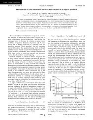
beams of opposite helicity detuned by δ as <strong>in</strong> Figure 2.1. The σ+ light<br />
¡ ¢£¤¥<br />
¡ ¢£ ¦<br />
<br />
©<br />
<br />
<br />
¡ ¢£§¥<br />
¡ ¢£ ¦<br />
¢£§¥ ¡ ¢£¤¥<br />
¡<br />
<br />
<br />
<br />
<br />
<br />
¡ ¨£ ¦<br />
Figure 2.1: Counter propagat<strong>in</strong>g σ+ <strong>an</strong>d σ− laser beams detuned from atomic<br />
reson<strong>an</strong>ce by δ are shown. The atomic levels are shifted due to the Zeem<strong>an</strong><br />
effect <strong>in</strong> a l<strong>in</strong>ear magnetic field. The effective detun<strong>in</strong>g for a stationary atom<br />
at position z ′ is δ± = δ ± geµBGmz ′ / as <strong>in</strong> Equations 2.10 <strong>an</strong>d 2.11.<br />
couples to the Mg = 0 −→ Me = +1 tr<strong>an</strong>sition <strong>an</strong>d the σ− light to the<br />
Mg = 0 −→ Me = −1. The effective detun<strong>in</strong>g, as <strong>in</strong> Equation 2.2, is<br />
δ± = δ ∓ kv ± (geMe − ggMg)µBB/, (2.11)<br />
<strong>in</strong> general, where Mg <strong>an</strong>d Me are Zeem<strong>an</strong> sub-levels of the ground <strong>an</strong>d excited<br />
states, <strong>an</strong>d gg <strong>an</strong>d ge are correspond<strong>in</strong>g L<strong>an</strong>dé g-factors, µB ∼ = h · 1.4 MHz/G<br />
11
is the Bohr magneton, h is Pl<strong>an</strong>ck’s const<strong>an</strong>t. The second term on the right of<br />
Equation 2.11 is due to the Doppler effect <strong>an</strong>d the third to the Zeem<strong>an</strong> effect.<br />
In the case of this simple example, of course, the Mg term on the right does<br />
not appear s<strong>in</strong>ce Mg = 0.<br />
The force that <strong>an</strong> atom feels <strong>in</strong> this situation is also described by Equa-<br />
tion 2.7 but now <strong>with</strong> δ± as def<strong>in</strong>ed <strong>in</strong> Equation 2.11 rather th<strong>an</strong> Equation<br />
2.6. This adds position dependence to F (<strong>in</strong> addition to velocity dependence):<br />
F (z, v) = 1<br />
<br />
I<br />
1<br />
1<br />
kΓ 2 −<br />
2 Is 1 + I/Is + (2δ+/Γ) 1 + I/Is + (2δ−/Γ) 2<br />
<br />
. (2.12)<br />
In the small velocity <strong>an</strong>d weak field limit, i.e. where v ≪ δ/k <strong>an</strong>d B ≪ δ/µB,<br />
Equation 2.12 c<strong>an</strong> be exp<strong>an</strong>ded:<br />
F (z, v) = 4k(I/Is)(2δ/Γ)<br />
[1 + I/Is + (2δ/Γ) 2 ] 2 (kv + (geµBGm/)z). (2.13)<br />
The equation of motion is therefore:<br />
where<br />
¨z + γtrap ˙z + ω 2 trapz = 0, (2.14)<br />
γtrap = 4k2 (I/Is)(2(−δ)/Γ)<br />
m [1 + I/Is + (2δ/Γ) 2 2 ,<br />
]<br />
ω 2 trap = 4k(geµBGm/)(I/Is)(2(−δ)/Γ)<br />
m [1 + I/Is + (2δ/Γ) 2 ] 2 ,<br />
(2.15)<br />
<strong>an</strong>d m is the atomic mass. In a MOT, the laser detun<strong>in</strong>g δ is red, so Equation<br />
2.14 is that of a damped harmonic oscillator. This motion c<strong>an</strong> be characterized<br />
by<br />
α ≡ γ2 trap<br />
4ω 2 trap<br />
=<br />
k3 (I/I0)(2(−δ)/Γ)<br />
(geµBGm/)m [1 + I/Is + (2δ/Γ) 2 2 . (2.16)<br />
]<br />
12
In a typical experimental situation, <strong>with</strong> Gm ≈ 10 G/cm <strong>an</strong>d δ ≈ 20 MHz, α<br />
is of order 100 which clearly makes the motion strongly over damped. Any<br />
displacement therefore decays exponentially towards the center.<br />
2.3 Magnetic Trapp<strong>in</strong>g<br />
Magnetic trapp<strong>in</strong>g is a result of the Zeem<strong>an</strong> effect. Classically, for <strong>an</strong><br />
atom <strong>with</strong> magnetic moment µ <strong>in</strong> magnetic field B(r), the potential energy is<br />
given by U(r) = −µ·B(r). The classical magnetic dipole, has some projection<br />
along B which is qu<strong>an</strong>tum mech<strong>an</strong>ically given by mF , that is, µ = ˆ B · µ =<br />
µBgF mF . Here, µB ∼ = h · 1.4 MHz/G is the Bohr magneton, gF is the L<strong>an</strong>dé g-<br />
factor, mF is the magnetic qu<strong>an</strong>tum number along the axis of the local B-Field,<br />
<strong>an</strong>d B is the magnitude [12]. The moment precesses around the local magnetic<br />
field at the Larmor frequency ωL = µB/. View<strong>in</strong>g each atom as a magnetic<br />
dipole moment, if the external magnetic field direction ch<strong>an</strong>ges slowly as <strong>an</strong><br />
atom moves through space, that is dθ/dt ≪ ωL, where θ is the <strong>an</strong>gle of the<br />
magnetic field <strong>with</strong> respect to some axis, the moment will adiabatically follow<br />
the field direction. The condition may also be written<br />
v · ∇B<br />
ωLB<br />
≪ 1. (2.17)<br />
Typically, <strong>with</strong> ∇B of at most order 250 G/cm, B at least 1 G, the above ratio<br />
c<strong>an</strong> be below 0.01 for atomic velocities of order several hundred recoil velocities.<br />
The adiabaticity condition, therefore, applies to atoms <strong>in</strong> a magnetic trap<br />
loaded from a MOT such as <strong>in</strong> the experiment system described here. For the<br />
13
87 Rb ground state 5 2 S1/2, the L<strong>an</strong>dé factors are gF =1 = −1/2 <strong>an</strong>d gF =2 = 1/2<br />
(see Figure F.1 <strong>in</strong> Appendix F). This me<strong>an</strong>s that the |F, mF 〉 states |2, 1〉,<br />
|2, 2〉, |1, −1〉 are low field seek<strong>in</strong>g states <strong>an</strong>d may be trapped. In the case of<br />
a magnetic trap <strong>with</strong> too weak a field, as discussed above, atoms of sufficient<br />
temperature will see a trapp<strong>in</strong>g field that varies too quickly <strong>an</strong>d may move to<br />
a different mF state (likely <strong>an</strong> untrapped state). Such tr<strong>an</strong>sitions are called<br />
Major<strong>an</strong>a flips <strong>an</strong>d result <strong>in</strong> trap loss. This is especially problematic for a trap<br />
<strong>with</strong> a field zero which results <strong>in</strong> Major<strong>an</strong>a flips for arbitrarily cold atoms.<br />
The depth of a magnetic trap is given by<br />
Ud = µ∆B, (2.18)<br />
where ∆B is the the difference between the field maximum (at the vacuum<br />
conta<strong>in</strong>er walls) <strong>an</strong>d the field m<strong>in</strong>imum where the atom cloud is centered.<br />
Typically, <strong>with</strong> a difference of ∆B order 10 G this gives a trap depth of order<br />
kB · 1 mK, where kB is the Boltzm<strong>an</strong>n const<strong>an</strong>t.<br />
Section 3.5 discusses the details of our magnetic trap. The field geome-<br />
tries of B(r) <strong>an</strong>d the trap oscillation frequencies are given there.<br />
2.4 <strong>Optical</strong> Trapp<strong>in</strong>g<br />
In general, the rotat<strong>in</strong>g wave approximation is valid where the second<br />
term <strong>in</strong> parenthesis of Equations 2.3 <strong>an</strong>d 2.4 may be neglected result<strong>in</strong>g <strong>in</strong><br />
U(r) = Γ2<br />
8Is<br />
14<br />
1<br />
I(r), (2.19)<br />
δ
<strong>an</strong>d<br />
R(r) = Γ3<br />
8Is<br />
ω<br />
ω0<br />
3 1<br />
I(r). (2.20)<br />
δ2 An import<strong>an</strong>t th<strong>in</strong>g to note here is that the dipole potential scales as I/δ <strong>an</strong>d<br />
the scatter<strong>in</strong>g rate as I/δ 2 . This me<strong>an</strong>s that the scatter<strong>in</strong>g rate may be made<br />
small by us<strong>in</strong>g a large detun<strong>in</strong>g. Even so, a high enough <strong>in</strong>tensity will allow<br />
for a strong dipole potential. This is how optical dipole traps are made. These<br />
are conservative traps, where scatter<strong>in</strong>g events do not occur on the time scale<br />
of the experiment.<br />
Far-off reson<strong>an</strong>ce lasers c<strong>an</strong> make attractive or repulsive potentials de-<br />
pend<strong>in</strong>g on detun<strong>in</strong>g. For light detuned red of reson<strong>an</strong>ce (of the D doublet for<br />
alkali atoms such as rubidium), the potential is attractive. For blue detun<strong>in</strong>gs,<br />
the potential is repulsive. This is because a ch<strong>an</strong>ge <strong>in</strong> sign of δ ch<strong>an</strong>ges the<br />
sign of U.<br />
2.5 Absorptive Imag<strong>in</strong>g<br />
An import<strong>an</strong>t method of imag<strong>in</strong>g atom clouds is <strong>with</strong> absorption imag-<br />
<strong>in</strong>g. The basic idea is that <strong>an</strong> atom cloud has some optical density to a near<br />
reson<strong>an</strong>t beam. We image this. Section 3.8.1 discusses absorptive imag<strong>in</strong>g <strong>in</strong><br />
context of our experimental setup. The idea is expla<strong>in</strong>ed here.<br />
Consider<strong>in</strong>g a near reson<strong>an</strong>t beam travel<strong>in</strong>g through a dilute cloud of<br />
15
atoms, the scattered power per unit volume is<br />
dI<br />
dz<br />
= −ωRn,<br />
= −σnI,<br />
(2.21)<br />
where n = n(x, y, z) is the atom number density, R is given by Equation 2.2,<br />
<strong>an</strong>d scatter<strong>in</strong>g cross section is<br />
σ = 3λ2<br />
2π<br />
This gives <strong>an</strong> exponential decay solution of the form<br />
<br />
I(x, y) = I0(x, y) exp −σ<br />
1<br />
. (2.22)<br />
1 + I/Is + (2δ/Γ) 2<br />
<br />
n(x, y, z)dz . (2.23)<br />
This <strong>in</strong>tensity distribution is imaged onto a CCD camera. This raw form<br />
qu<strong>an</strong>tity conta<strong>in</strong>s two-dimensional spatial <strong>in</strong>formation about the density of<br />
the atom cloud. Section 3.8.1 discusses extraction of <strong>in</strong>formation from I(x, y)<br />
<strong>an</strong>d experimental implementation. Most of the atom cloud images described<br />
<strong>in</strong> this thesis were made <strong>with</strong> this method.<br />
16
Chapter 3<br />
Experimental Apparatus<br />
This chapter <strong>in</strong>troduces m<strong>an</strong>y of the major devices <strong>an</strong>d techniques of<br />
the experimental system. These <strong>in</strong>clude the vacuum system, the laser systems,<br />
the magnetic trap, the computer control system, <strong>an</strong>d the imag<strong>in</strong>g techniques.<br />
The experimental sequence up to BEC production <strong>in</strong> the magnetic trap is also<br />
discussed <strong>in</strong> this chapter.<br />
3.1 Introduction<br />
The vacuum chamber <strong>an</strong>d most lasers <strong>an</strong>d optics are on a 12 ′ ×5 ′ optical<br />
table shown <strong>in</strong> Figure 3.1. The table holds thous<strong>an</strong>ds of optical elements,<br />
dozens of optical modulators, dozens of mech<strong>an</strong>ical shutters, all five of the near<br />
reson<strong>an</strong>ce lasers (Section 3.3), the <strong>in</strong>frared far-off reson<strong>an</strong>ce laser (Section 3.4).<br />
The experiment shares a secondary table <strong>with</strong> the Sodium BEC experiment<br />
[13]. This table is shown <strong>in</strong> Figure 3.2. It is <strong>an</strong> 8 ′ × 4 ′ optical table <strong>an</strong>d is<br />
the site of the Verdi laser — our other far-off reson<strong>an</strong>ce laser (Section 3.4).<br />
A waveplate on a computer controlled tr<strong>an</strong>slation stage <strong>in</strong> conjunction <strong>with</strong> a<br />
polariz<strong>in</strong>g beam splitter cube sends the beam to either one of the experiments.<br />
The follow<strong>in</strong>g sections describe the major parts of the experimental<br />
17
Figure 3.1: The ma<strong>in</strong> optical table. The table is divided <strong>in</strong>to two section. The<br />
image on the left shows the section of table devoted to the lasers. The image<br />
on the right shows the section for the vacuum chamber.<br />
Figure 3.2: The shared optical table. It holds the Verdi laser as well as some<br />
of the beam control optics for that laser. A box constructed from black foam<br />
board surrounds most of the optics to protect the beam from air currents <strong>an</strong>d<br />
shield aga<strong>in</strong>st scattered light.<br />
18
apparatus <strong>in</strong> more detail. There are also signific<strong>an</strong>t technical appendices which<br />
provide greater detail on some of the specifics of various designs.<br />
3.2 Vacuum Chamber<br />
Our vacuum chamber was designed to be used as a double MOT sys-<br />
tem [14]. The upper chamber is used as a vapor cell MOT where the atoms<br />
are captured from a background of rubidium vapor. This is a high pressure<br />
region (of order 10 −7 torr); a differential pump<strong>in</strong>g tube provides a connection<br />
to the lower chamber <strong>an</strong>d ma<strong>in</strong>ta<strong>in</strong>s more th<strong>an</strong> three orders of magnitude of<br />
pressure difference <strong>with</strong> the lower chamber. The lower chamber is <strong>an</strong> ultra-<br />
high vacuum region (UHV); it conta<strong>in</strong>s the vacuum pumps <strong>an</strong>d the science<br />
chamber [15]. These items are all discusses <strong>in</strong> this section. Figures 3.6 <strong>an</strong>d<br />
3.7 show photographs of the upper chamber <strong>an</strong>d the science chamber <strong>in</strong> the<br />
experimental setup. Figure 3.8 shows a photograph of the vacuum chamber<br />
before other experiment components were added.<br />
3.2.1 Upper Chamber<br />
The upper chamber consists of a glass cell <strong>an</strong>d is separated from the<br />
lower chamber by a differential pump<strong>in</strong>g tube. The upper chamber is shown<br />
schematically <strong>in</strong> Figure 3.3. The glass cell is 4 ′′ × 1.25 ′′ × 1.25 ′′ <strong>an</strong>d made of<br />
Pyrex. It is attached by a graded glass-to-metal seal to a 2.75 ′′ steel fl<strong>an</strong>ge. The<br />
seal is from Larson Electronic Glass Inc. <strong>an</strong>d Technical Glass Inc. performed<br />
the assembly. We operate a vapor cell Magneto-optical trap (MOT) <strong>in</strong> this<br />
19
Rb<br />
Source<br />
Pyrex Cell<br />
Push beam<br />
Lower Chamber<br />
Diagonal upper<br />
MOT beams<br />
Upper MOT atoms<br />
Differential<br />
pump<strong>in</strong>g tube<br />
Glass-to-metal seal<br />
Figure 3.3: The upper chamber consists of a glass cell <strong>an</strong>d is separated from<br />
the lower chamber by a differential pump<strong>in</strong>g tube. The orientation of the<br />
diagonal upper MOT beams is shown. The horizontal beam pair is omitted<br />
from the figure, they counterpropogate perpendicular to the pl<strong>an</strong>e of the paper.<br />
The push beam hits the atoms from above <strong>an</strong>d is focused to pass through the<br />
differential pump<strong>in</strong>g tube. The vertical absorption imag<strong>in</strong>g beam also follows<br />
a similar path (see Section 3.8.1).<br />
20
chamber. The MOT consists of 3 pairs of counter propagat<strong>in</strong>g beams: 2<br />
diagonal pairs <strong>an</strong>d one horizontal pair. This forms a st<strong>an</strong>dard six-beam MOT.<br />
As <strong>in</strong> Ref. [14], we use <strong>an</strong> additional beam, the push beam, to produce <strong>an</strong><br />
atom funnel situation. Here, the atoms are captured from the background<br />
vapor <strong>an</strong>d then stream through the differential pump<strong>in</strong>g tube <strong>in</strong>to the lower<br />
chamber where they are recaptured <strong>an</strong>d used for experiments. More details<br />
are expla<strong>in</strong>ed <strong>in</strong> Section 3.7.<br />
The upper chamber operates near the room temperature vapor pressure<br />
of rubidium, around 10 −7 torr. This high pressure is required to allow for a<br />
signific<strong>an</strong>t number of atoms <strong>in</strong> the capture velocity r<strong>an</strong>ge of the MOT (order<br />
10 m/s). So, <strong>in</strong> fact, the MOT captures only the low velocity tail of a room<br />
temperature velocity distribution. The extra atoms which are not captured<br />
only serve as a collisional loss mech<strong>an</strong>ism to the traps. It is for this reason that<br />
a differential pump<strong>in</strong>g tube is employed which separates the science chamber<br />
from this high pressure load<strong>in</strong>g chamber. The tube consists of a 6 ′′ 304 sta<strong>in</strong>-<br />
less steel rod which has been drilled to have a 1/8 ′′ hole at the top <strong>an</strong>d the<br />
hole widens out <strong>with</strong> <strong>an</strong> <strong>an</strong>gle of about 2 ◦ . This is <strong>in</strong>tended to <strong>in</strong>crease the<br />
solid <strong>an</strong>gle for the pushed atoms yet keep the vacuum conduct<strong>an</strong>ce low. The<br />
conduct<strong>an</strong>ce of this tube is order 0.05 liters/s which leads to greater th<strong>an</strong> three<br />
orders of magnitude of pressure difference. Despite be<strong>in</strong>g <strong>an</strong> efficient block for<br />
the thermal atoms <strong>in</strong> the upper chamber, the MOT atoms may be pushed <strong>in</strong>to<br />
the lower chamber <strong>with</strong> high efficiency. It is these atoms which are loaded <strong>in</strong>to<br />
the lower MOT <strong>an</strong>d used to make condensates.<br />
21
It is worth not<strong>in</strong>g that this upper chamber <strong>in</strong>volv<strong>in</strong>g the pyrex glass cell<br />
is the newest version of the upper chamber which <strong>in</strong> the past had problematic<br />
versions. Previous generations used a steel upper chamber which had Kovar<br />
sealed zero-length w<strong>in</strong>dows. These w<strong>in</strong>dows are st<strong>an</strong>dard <strong>an</strong>d available from<br />
m<strong>an</strong>y vacuum comp<strong>an</strong>ies. The problem was that the seals decayed over time<br />
— they formed small cracks. In some cases, this was temporarily fixed by the<br />
use of Vacseal (a vacuum compatible brush-on seal<strong>an</strong>t) <strong>an</strong>d/or by form<strong>in</strong>g <strong>an</strong><br />
auxiliary vacuum chamber outside the w<strong>in</strong>dow for differential pump<strong>in</strong>g. In<br />
our experiences, these quick fixes provided a life support for the chamber for<br />
some period of time from weeks to months, but ultimately had to be replaced<br />
<strong>with</strong> the design we have here. It is likely that the problems that occurred <strong>in</strong><br />
our previous upper chambers were due to a reaction <strong>with</strong> the rubidium metal<br />
present. A primary concern here is the relatively high rubidium vapor pressure<br />
<strong>in</strong> the upper chamber (of order 10 −7 torr). It is likely that the rubidium ate<br />
away at the seals of the zero-length viewports. The seal of the glass cell upper<br />
chamber described <strong>in</strong> this section is of a different sort <strong>an</strong>d has a larger seal<strong>in</strong>g<br />
area. A glass cell <strong>with</strong> this sort of seal <strong>in</strong> a similar sett<strong>in</strong>g has produced years<br />
of reliable service [16].<br />
3.2.2 Lower Chamber<br />
The lower chamber consists of two regions. One is the pump<strong>in</strong>g re-<br />
gion. This is the location of the ion pump <strong>an</strong>d the Tit<strong>an</strong>ium sublimation<br />
(Ti:sub) pump. These pumps ma<strong>in</strong>ta<strong>in</strong> the lower chamber at a pressure below<br />
22
10 −10 torr. The science chamber is a high quality glass cell that is attached<br />
to the bottom of the lower chamber pump region. This is the location of the<br />
lower MOT, magnetic trap, <strong>an</strong>d optical trap procedures.<br />
3.2.2.1 Pump<strong>in</strong>g Region<br />
The pump<strong>in</strong>g region is shown schematically <strong>in</strong> Figure 3.4. The cen-<br />
ter component of this chamber region is a modified six-way steel cross <strong>with</strong><br />
4.5 ′′ fl<strong>an</strong>ges supplemented by 1.5 ′′ tubes <strong>with</strong> 2.75 ′′ fl<strong>an</strong>ges. This piece was<br />
orig<strong>in</strong>ally used <strong>in</strong> the cesium experiments by our predecessors [17–19]. The<br />
pumps run cont<strong>in</strong>uously. The ion pump from Vari<strong>an</strong> has a pump<strong>in</strong>g speed of<br />
75 liters/s. The Ti:sublimation pump has a pump<strong>in</strong>g speed which depends on<br />
the surface area of the steel tube which conta<strong>in</strong>s it <strong>an</strong>d also on the cle<strong>an</strong>l<strong>in</strong>ess<br />
of the Tit<strong>an</strong>ium getter material deposited there. In normal operation, this<br />
pump has a speed of around 300 leters/s. This pump is flashed on as needed.<br />
There is also a Bayard-Alpert ion gauge, which was used for diagnostics <strong>in</strong><br />
some of the <strong>in</strong>itial stages of the chamber after the evacuation/bakeout pro-<br />
cedure. In pr<strong>in</strong>ciple, this gauge c<strong>an</strong> read pressures <strong>in</strong> the 10 −10 torr r<strong>an</strong>ge,<br />
but <strong>in</strong> practice, the operation of the gauge partially spoils the vacuum. The<br />
most sensitive pressure measurement we have, <strong>an</strong>d the only relev<strong>an</strong>t vacuum<br />
measurement is the atom lifetime <strong>in</strong> the magnetic trap. When the vacuum<br />
chamber is healthy, this is typically greater th<strong>an</strong> one m<strong>in</strong>ute.<br />
23
Ion Pump<br />
TSP<br />
Ion Gauge<br />
Ion Pump<br />
Figure 3.4: The UHV pump<strong>in</strong>g region. Attached to the ma<strong>in</strong> vacuum chamber<br />
are two pumps <strong>an</strong>d <strong>an</strong> ion gauge. Directly below this region is the science<br />
chamber (not shown here, see Figure 3.5). The upper draw<strong>in</strong>g is a side view<br />
<strong>an</strong>d the lower draw<strong>in</strong>g is a top view.<br />
24
Figure 3.5: The lower chamber. The glass cell is where the experiments take<br />
place. The metal adaptor <strong>an</strong>d the gold colored helicoflex seals connect the<br />
glass cell to the lower chamber pump<strong>in</strong>g region.<br />
3.2.2.2 Science Chamber Region<br />
The science chamber consists of a high quality glass cell which is at-<br />
tached directly below the pump<strong>in</strong>g region of the lower chamber. The ex-<br />
perimental apparatus really centers around this location. The cell is shown<br />
schematically <strong>in</strong> Figure 3.5. The cell itself has outer dimensions 30 × 30 ×<br />
115 mm <strong>with</strong> 5 mm thick walls. The material is Spectrosil, a synthetic fused<br />
silica. The cell is attached to a 75 mm diameter, 17 mm thick circular fl<strong>an</strong>ge of<br />
the same material. The center of the fl<strong>an</strong>ge has a 20 mm diameter hole drilled<br />
to make contact <strong>with</strong> the pump<strong>in</strong>g region. It was m<strong>an</strong>ufactured by Helma<br />
Cells Inc. which uses impressive fabrication techniques. They polish the sides<br />
<strong>an</strong>d optically contact the cell together. It is then fired near the material melt-<br />
<strong>in</strong>g po<strong>in</strong>t to fuse the edges. This is all done <strong>with</strong>out <strong>an</strong>y cement<strong>in</strong>g material so<br />
25
the w<strong>in</strong>dows are left very cle<strong>an</strong> of auxiliary material. The upper glass fl<strong>an</strong>ge<br />
is attached to the steel chamber by the use of a Helicoflex seal. These seals<br />
(Garlock-Helicoflex part H-307330 REV NC) consist of a helical spr<strong>in</strong>g <strong>with</strong><br />
a metal l<strong>in</strong><strong>in</strong>g. The top <strong>an</strong>d bottom of the seals have a delta shaped ridge.<br />
When compressed to some specified dist<strong>an</strong>ce, the ridge bites <strong>in</strong>to the materials<br />
on each side to form a good seal <strong>an</strong>d the spr<strong>in</strong>g acts as a restor<strong>in</strong>g force aga<strong>in</strong>st<br />
compression. The ridge effectively bonds <strong>with</strong> the glass of the fl<strong>an</strong>ge on one<br />
side <strong>an</strong>d the steel receptacle piece on the other. In this setup, we used two of<br />
these circular seals, one makes the actual seal (top <strong>in</strong> Figure 3.5), <strong>an</strong>d a lower<br />
one which acts as a cushion aga<strong>in</strong>st the counter steel part which pushes up<br />
on the glass fl<strong>an</strong>ge. Altogether this procedure makes <strong>an</strong> effective UHV seal,<br />
which has only shown problems <strong>in</strong> the case of a bak<strong>in</strong>g procedure which may<br />
<strong>in</strong>volve too quick thermal ch<strong>an</strong>ges.<br />
26
Glass Cell<br />
Magnet Coils<br />
Differential<br />
Pump<strong>in</strong>g Tube<br />
Figure 3.6: The upper chamber consists of a glass cell. The photograph also<br />
shows the top of the differential pump<strong>in</strong>g tube <strong>in</strong>side the chamber. The vapor<br />
cell MOT is formed here from the background vapor, the quadrupole coil pair<br />
of the upper MOT is visible.<br />
Science chamber<br />
Quadrupole coils<br />
S<strong>in</strong>gle atom<br />
detection optics<br />
Ioffe coil<br />
Figure 3.7: The science chamber consists of a glass cell. The QUIC trap coils<br />
are visible <strong>in</strong> the photo as well as the <strong>in</strong>itial optics for the s<strong>in</strong>gle atom detection<br />
system.<br />
27
Upper Chamber<br />
Differential<br />
pump<strong>in</strong>g tube<br />
Rb source<br />
Ion pump<br />
Ti:sub pump<br />
Science Chamber<br />
Figure 3.8: The vacuum chamber. This photo shows the vacuum chamber on<br />
the optical table before all of the obstacles are <strong>in</strong>stalled.<br />
28
3.3 The Near Reson<strong>an</strong>ce Lasers<br />
The near reson<strong>an</strong>ce lasers are used for the operation of the MOTs,<br />
absorption imag<strong>in</strong>g, <strong>an</strong>d optical pump<strong>in</strong>g. The various wavelengths relative to<br />
the level structure are shown <strong>in</strong> Figure 3.9. The figure also shows the far-off<br />
reson<strong>an</strong>ce lasers (Section 3.4).<br />
The near reson<strong>an</strong>ce lasers are all around the D2 l<strong>in</strong>e of rubidium 87<br />
at about 780 nm. The laser system consists of several dist<strong>in</strong>ct parts. One<br />
is the Littrow configuration master diode lasers which are locked onto the<br />
MOT <strong>an</strong>d repump tr<strong>an</strong>sitions by saturation absorption spectroscopy methods.<br />
The other part is the set of three <strong>in</strong>jection locked (slave) diode lasers which<br />
supply the actual MOT light. These lasers <strong>an</strong>d their generated beam paths<br />
are discussed <strong>in</strong> this section. The properties of the diodes used for these<br />
lasers are summarized <strong>in</strong> Table 3.1. All of the diodes produce a 3:1 spatially<br />
elliptical beam which is corrected <strong>in</strong> each case by <strong>an</strong> <strong>an</strong>amorphic prism pair.<br />
All lasers are followed by some number of acousto-optic modulators (AOM)<br />
which are used for frequency tun<strong>in</strong>g <strong>an</strong>d <strong>in</strong>tensity control. Because the AOM<br />
<strong>in</strong>tensity control is very fast, they act as fast, but imperfect beam shutters.<br />
When operat<strong>in</strong>g the magnetic trap or optical trap, the chamber must be dark<br />
of the near reson<strong>an</strong>t light s<strong>in</strong>ce this c<strong>an</strong> cause major heat<strong>in</strong>g <strong>an</strong>d trap loss.<br />
Even <strong>with</strong> RF switches on the drive of the AOMs, there is some light leakage<br />
<strong>in</strong>to the diffracted orders of the AOMs which results <strong>in</strong> the need of additional<br />
home-built mech<strong>an</strong>ical shutters [20] to block the residual light.<br />
29
780.2 nm<br />
F=2<br />
F=1<br />
6.83 GHz<br />
1064 nm YAG<br />
532 nm doubled YAG<br />
Absorption Imag<strong>in</strong>g Beam<br />
MOT Beam<br />
<strong>Optical</strong> Pump<strong>in</strong>g Beam<br />
Repump Beam<br />
266.7 MHz<br />
156.9 MHz<br />
F'=3<br />
F'=2<br />
F'=1<br />
72.2 MHz<br />
F'=0<br />
Figure 3.9: D2 l<strong>in</strong>e diagram shown <strong>with</strong> the multitude of laser frequencies used<br />
<strong>in</strong> the experiment. The near reson<strong>an</strong>ce laser are discussed <strong>in</strong> Section 3.3 <strong>an</strong>d<br />
the far-off reson<strong>an</strong>ce lasers <strong>in</strong> Section 3.4. Diagram not to scale.<br />
30
Laser Diodes<br />
property MLD780-100S5P GH0781JA2C<br />
distributor Intelite, Inc. Digi-Key<br />
nom<strong>in</strong>al wavelength 780 nm 784 nm<br />
maximum output power 100mW 120mW<br />
threshold current 30mA 30mA<br />
operat<strong>in</strong>g current 120mA 140mA<br />
maximum operat<strong>in</strong>g current 140mA 167mA<br />
maximum reverse voltage 2V 2V<br />
m<strong>an</strong>ufacturer Sharp<br />
Table 3.1: Characteristics of the lasers diodes used <strong>in</strong> the experiment. The<br />
Intelite diodes are used <strong>in</strong> the grat<strong>in</strong>g stabilized MOT master <strong>an</strong>d repump.<br />
The Digikey diodes are used <strong>in</strong> the <strong>in</strong>jection locked slave lasers. Note that the<br />
784 nm nom<strong>in</strong>al wavelength is brought near 780 nm by controll<strong>in</strong>g the diode<br />
temperature.<br />
3.3.1 The Grat<strong>in</strong>g Stabilized Lasers<br />
The construction of the MOT master <strong>an</strong>d the repump lasers are similar.<br />
The design is a modified version of the lasers used <strong>in</strong> the previous cesium<br />
experiment [17–19] for the rubidium wavelength (grat<strong>in</strong>g <strong>an</strong>gle ch<strong>an</strong>ged). One<br />
of the lasers is shown <strong>in</strong> Figure 3.10. Both the MOT master <strong>an</strong>d the repump<br />
laser are grat<strong>in</strong>g stabilized lasers. The Plexiglass cover is used to provide some<br />
amount of thermal isolation from the environment <strong>an</strong>d the brass blocks that<br />
compose the device are temperature stabilized actively <strong>with</strong> a thermoelectric<br />
cooler <strong>an</strong>d a PID circuit. In this structure, the diode itself is the MLD780-<br />
100S5P <strong>in</strong> Table 3.1 <strong>an</strong>d is conta<strong>in</strong>ed <strong>in</strong>side a Thorlabs collimation tube (model<br />
LT230P-B). The idea is to use the specular reflection from the grat<strong>in</strong>g as the<br />
output beam whereas the diffracted beam feeds back <strong>in</strong>to the diode to form <strong>an</strong><br />
31
Figure 3.10: The master lasers. Both the MOT master <strong>an</strong>d the repump laser<br />
are grat<strong>in</strong>g stabilized lasers. The Plexiglass cover is used to provide thermal<br />
isolation from the environment.<br />
32
103MHz<br />
44MHz<br />
AOM<br />
AOM<br />
Figure 3.11: The MOT master laser lock<strong>in</strong>g setup. A small portion of the MOT<br />
master beam is sent through the depicted saturation absorption spectroscopy<br />
setup.<br />
external cavity. This allows the output wavelength to be tuned <strong>with</strong> grat<strong>in</strong>g<br />
<strong>an</strong>gle. The Littrow <strong>an</strong>gle, α, is given by [21]<br />
Rb<br />
mλ = 2d s<strong>in</strong> α, (3.1)<br />
where m = 1 is the diffraction order we use, λ = 780 nm, d = 0.833 µm is the<br />
l<strong>in</strong>e spac<strong>in</strong>g of the grat<strong>in</strong>g (1200 l<strong>in</strong>es/mm). This gives α ∼ = 27.9 ◦ . The grat<strong>in</strong>g<br />
is mounted so it may be grossly positioned by mech<strong>an</strong>ical screws m<strong>an</strong>ually, <strong>an</strong>d<br />
may be f<strong>in</strong>e adjusted by the voltage on a piezo-electric tr<strong>an</strong>sducer stage.<br />
33<br />
PD
3.3.1.1 The MOT Master Laser<br />
The MOT master is frequency locked us<strong>in</strong>g the setup shown <strong>in</strong> Figure<br />
3.11, a version of the st<strong>an</strong>dard saturation absorption spectroscopy setup [22,<br />
23]. Some amount of light is picked off by the 103 MHz AOM (also shown <strong>in</strong><br />
Figure 3.13). This 1 mW first order beam is frequency upshifted by 103 MHz.<br />
The beam is split so that part double passes a frequency modulated AOM<br />
<strong>with</strong> 44 MHz center frequency <strong>with</strong> modulation frequency of 50 kHz over the<br />
r<strong>an</strong>ge between 40 MHz <strong>an</strong>d 48 MHz. Due to the curved mirror retroreflection,<br />
the output beam may be modulated <strong>with</strong>out walk<strong>in</strong>g the beam position. The<br />
modulated beam counterpropogates <strong>with</strong> the unmodulated beam <strong>in</strong> a rubidium<br />
absorption cell <strong>an</strong>d then is detected by a photodiode. In the cell, the two beams<br />
<strong>in</strong>teract <strong>with</strong> a velocity class of atoms correspond<strong>in</strong>g to a frequency shift of<br />
44 MHz.<br />
The result<strong>an</strong>t signal of the spectroscopy setup is shown <strong>in</strong> Figure 3.12.<br />
The signal shows the Doppler free structure of the l<strong>in</strong>e <strong>with</strong> tr<strong>an</strong>sitions between<br />
the F = 2 ground state to the excited states F ′ = 1, 2, 3 <strong>an</strong>d the cross-over<br />
tr<strong>an</strong>sitions. This F = 2 → F ′ group has a spectral width of about 425 MHz.<br />
The laser is locked to the F = 2 → F ′ = 2/3 crossover tr<strong>an</strong>sition because<br />
it is the strongest l<strong>in</strong>e <strong>in</strong> the dispersive signal. This l<strong>in</strong>e is 133 MHz red of<br />
the F = 2 → F ′ = 3 cycl<strong>in</strong>g tr<strong>an</strong>sition required for the MOT light. Because<br />
the <strong>in</strong>itial pick-off AOM shifts the beam up by 103 MHz <strong>an</strong>d the light is then<br />
shifted up <strong>an</strong> additional 44 MHz by the double passed AOM, the MOT master<br />
laser is then locked 280 MHz red of the F = 2 → F ′ = 3 cycl<strong>in</strong>g tr<strong>an</strong>sition.<br />
34
Intensity<br />
a b c d e f<br />
Frequency<br />
Figure 3.12: The MOT saturated absorption spectroscopy dispersive signal.<br />
The different dispersive l<strong>in</strong>eshapes refer to the follow<strong>in</strong>g tr<strong>an</strong>sitions: a)F =<br />
2 → F ′ = 1, b)F = 2 → F ′ = 1/2, c)F = 2 → F ′ = 2, d)F = 2 → F ′ = 1/3,<br />
e)F = 2 → F ′ = 2/3, f)F = 2 → F ′ = 3.<br />
35
The MOT master light is distributed to the slave lasers as shown <strong>in</strong><br />
Figure 3.13. The power that does not go to the saturation lock<strong>in</strong>g setup<br />
receives additional frequency shift<strong>in</strong>g by <strong>an</strong> 80 MHz double pass AOM <strong>with</strong><br />
40 MHz b<strong>an</strong>dwidth. The result<strong>an</strong>t seed light for the <strong>in</strong>jection locked slave<br />
lasers is then between 80 MHz <strong>an</strong>d 160 MHz red of the F = 2 → F ′ = 3<br />
cycl<strong>in</strong>g tr<strong>an</strong>sition. Because each slave laser is followed by its own 80 MHz<br />
s<strong>in</strong>gle pass AOM (see Section 3.3.2), the output light will be between reson<strong>an</strong>ce<br />
<strong>an</strong>d 80 MHz red of the cycl<strong>in</strong>g tr<strong>an</strong>sition. This allows for various beams to be<br />
generated <strong>in</strong>clud<strong>in</strong>g the absorption beams (on reson<strong>an</strong>ce), the MOT beams<br />
(3Γ = 18 MHz from reson<strong>an</strong>ce), <strong>an</strong>d polarization gradient cool<strong>in</strong>g light (at<br />
up to 60 MHz red of reson<strong>an</strong>ce). The specifics of these <strong>an</strong>d other beams are<br />
discussed <strong>with</strong> the slave laser setups, see Section 3.3.2.<br />
3.3.1.2 The Repump Laser<br />
For the repump laser, we are <strong>in</strong>terested <strong>in</strong> the F = 1 → F ′ tr<strong>an</strong>sitions<br />
which have a spectral width of about 230 MHz. The Doppler free profile is<br />
shown <strong>in</strong> Figure 3.14. Specifically, the desired repump tr<strong>an</strong>sition is F = 1 →<br />
F ′ = 2. For the atoms which end up <strong>in</strong> the F = 1 ground state, this laser<br />
‘repumps’ them back <strong>in</strong>to the cycl<strong>in</strong>g state. The problem is that <strong>with</strong>out the<br />
repump light, atoms are eventually pumped <strong>in</strong>to this dark state <strong>an</strong>d the MOTs<br />
do not work well.<br />
Because it is the strongest l<strong>in</strong>e, the repump is locked us<strong>in</strong>g the F =<br />
1 → F ′ = 1/2 crossover tr<strong>an</strong>sition. This results <strong>in</strong> laser output 78.5 MHz<br />
36
To Fabry-Perot Cavity<br />
AOM<br />
80MHz<br />
To Slave Lasers<br />
To Absorption Lock<br />
AOM<br />
103 MHz<br />
Figure 3.13: MOT master laser distribution scheme. The diode laser assembly<br />
appears on the right followed by <strong>an</strong> optical isolator. The light from the MOT<br />
master laser goes through different frequency shift<strong>in</strong>g devices <strong>in</strong> order to correctly<br />
set the frequency of the light before it is used to <strong>in</strong>jection lock the slave<br />
lasers.<br />
37
Intensity<br />
a<br />
b<br />
c d<br />
Frequency<br />
Figure 3.14: Repump saturated absorption profile. The different dispersive<br />
l<strong>in</strong>eshapes refer to the follow<strong>in</strong>g tr<strong>an</strong>sitions: a)F = 1 → F ′ = 0, b)F = 1 →<br />
F ′ = 0/1, c)F = 1 → F ′ = 1, d)F = 1 → F ′ = 0/2, e)F = 1 → F ′ = 1/2,<br />
f)F = 1 → F ′ = 2.<br />
red of the repump l<strong>in</strong>e (F = 1 → F ′ = 2). The light is distributed to the<br />
upper <strong>an</strong>d lower MOTs as <strong>in</strong> Figure 3.15. The 80 MHz AOM shifts the light<br />
to 1.5 MHz blue of the reson<strong>an</strong>ce which has little operational effect. This light<br />
is directly sent to the MOTs for repump<strong>in</strong>g. Typically, we send 5 mW to the<br />
upper MOT <strong>an</strong>d 4 mW to the lower MOT.<br />
3.3.2 Injection Locked MOT Lasers<br />
e<br />
In order to provide sufficient MOT light for the upper <strong>an</strong>d lower MOTs,<br />
we use <strong>in</strong>jection locked lasers. Alone, these lasers are free runn<strong>in</strong>g lasers near<br />
780 nm. We use the GH0781JA2C diodes <strong>in</strong> Table 3.1. Although the diodes are<br />
‘nom<strong>in</strong>ally’ specified to free run at 784 nm, the free runn<strong>in</strong>g wavelength may be<br />
adjusted <strong>with</strong> temperature. We chose these diodes because of their high power,<br />
38<br />
f
To Upper MOT<br />
To Lower MOT<br />
λ/2<br />
To Fabry-Perot Cavity<br />
AOM<br />
80MHz<br />
λ/2<br />
To Absorption Lock<br />
Figure 3.15: The distribution network for the repump grat<strong>in</strong>g stabilized laser.<br />
The diode laser assembly appears on the right followed by <strong>an</strong> optical isolator.<br />
availability, <strong>an</strong>d low cost. The diodes are held <strong>in</strong> a Thorlabs collimation tube<br />
(LT230P-B) which is housed <strong>in</strong> a temperature controlled bronzed alum<strong>in</strong>um<br />
block. This block sits atop a thermal electric cooler (TEC) which is controlled<br />
by a PID circuit. An <strong>an</strong>odized alum<strong>in</strong>um hous<strong>in</strong>g acts as a heat s<strong>in</strong>k for the<br />
TEC <strong>an</strong>d hold <strong>an</strong> output brewster w<strong>in</strong>dow. A slave laser is shown <strong>in</strong> Figure<br />
3.16.<br />
The slaves are locked us<strong>in</strong>g the light from the MOT master laser. The<br />
method of <strong>in</strong>jection lock<strong>in</strong>g <strong>in</strong>volves send<strong>in</strong>g a small amount of light <strong>in</strong>to the<br />
diode which is matched well spatially to the diode output [22, 24]. The <strong>in</strong>jec-<br />
tion light is sent <strong>in</strong>to the reject port of the optical isolator which is placed after<br />
each slave laser. We typically use around 2 mW of <strong>in</strong>jection power. There are<br />
39
Figure 3.16: Pictures of the slave lasers. The image on the right shows the<br />
slave laser hous<strong>in</strong>g complete <strong>with</strong> the outer cover<strong>in</strong>g. The image on the left<br />
shows the hous<strong>in</strong>g m<strong>in</strong>us the cover allow<strong>in</strong>g one to see the laser diode holder<br />
as well as the electrical connections.<br />
three <strong>in</strong>jection locked slave lasers. Their layouts are discussed <strong>in</strong> the follow<strong>in</strong>g<br />
sections. Each slave uses a 3:1 <strong>an</strong>amorphic prism pair for beam shap<strong>in</strong>g <strong>an</strong>d<br />
a ConOptics optical isolator (model 712B).<br />
3.3.2.1 Upper MOT Horizontal Slave Laser<br />
The upper MOT horizonal laser also supplies the light for the vertical<br />
imag<strong>in</strong>g beam <strong>an</strong>d the push beam as shown <strong>in</strong> Figure 3.17.<br />
The first order of the 80 MHz AOM provides the upper MOT light.<br />
This AOM also serves as a beam <strong>in</strong>tensity control <strong>an</strong>d fast shutter. There is<br />
also a mech<strong>an</strong>ical shutter which blocks the MOT light when the atoms are to<br />
be <strong>in</strong> the dark. Even <strong>with</strong> <strong>an</strong> RF switch, the AOM has some level of leakage<br />
light <strong>in</strong>to the first order.<br />
The zeroth order beam from this AOM is then used for the vertical<br />
40
λ/2<br />
Vertical<br />
Imag<strong>in</strong>g<br />
Push Beam<br />
To<br />
Fabry-Perot<br />
Upper MOT<br />
Horizontal<br />
From MOT<br />
Master<br />
To Other<br />
Slaves<br />
80MHz<br />
AOM<br />
<strong>Optical</strong><br />
Isolator<br />
40MHz<br />
AOM<br />
Upper MOT<br />
Horizontal<br />
Slave Laser<br />
56MHz<br />
λ/4<br />
AOM<br />
Figure 3.17: Beam distribution for the upper MOT horizontal slave laser.<br />
41
imag<strong>in</strong>g <strong>an</strong>d the push beam. The push beam is put near the MOT reson<strong>an</strong>ce<br />
by the 40 MHz double passed AOM <strong>an</strong>d sent <strong>in</strong>to the top port of the upper<br />
chamber. The zeroth order of this AOM double passes a 56 MHz AOM which<br />
puts the vertical absorption imag<strong>in</strong>g beam on reson<strong>an</strong>ce <strong>with</strong> appropriate set-<br />
t<strong>in</strong>g of the MOT master laser. This beam also enters the chamber through<br />
the top port of the upper chamber.<br />
3.3.2.2 Upper MOT Diagonal Slave Laser<br />
The upper MOT diagonal laser also supplies the light for the horizontal<br />
imag<strong>in</strong>g beam <strong>an</strong>d the optical pump<strong>in</strong>g beam as shown <strong>in</strong> Figure 3.18.<br />
The first order of the 80 MHz AOM provides the upper MOT light. This<br />
AOM also serves as a beam <strong>in</strong>tensity control <strong>an</strong>d fast shutter. In addition,<br />
there is a mech<strong>an</strong>ical shutter which blocks the MOT light when the atoms are<br />
to be <strong>in</strong> the dark as <strong>with</strong> the horizontal laser.<br />
The zeroth order beam from this AOM is then used for the other two<br />
beams. The imag<strong>in</strong>g beam is put on the MOT reson<strong>an</strong>ce by the 56 MHz<br />
double passed AOM <strong>an</strong>d sent horizontally through the science chamber to<br />
make images. The zeroth order of this AOM double passes through a 80 MHz<br />
AOM us<strong>in</strong>g the m<strong>in</strong>us first order. This lowers the frequency by 160 MHz which<br />
puts the beam <strong>in</strong> the r<strong>an</strong>ge so that <strong>with</strong> appropriate master laser sett<strong>in</strong>g dur<strong>in</strong>g<br />
the sequence, the light will be on the F = 2 → F ′ = 2 tr<strong>an</strong>sition for optical<br />
pump<strong>in</strong>g. Both horizontal imag<strong>in</strong>g beam <strong>an</strong>d optical pump<strong>in</strong>g beam follow<br />
similar paths <strong>an</strong>d have 15 mm waists at the location of the atoms.<br />
42
<strong>Optical</strong> Pump<strong>in</strong>g <strong>an</strong>d<br />
Absorptive Imag<strong>in</strong>g<br />
λ/2<br />
Upper MOT<br />
Diagonal<br />
From MOT<br />
Master<br />
To Other Slaves<br />
80MHz<br />
AOM<br />
<strong>Optical</strong><br />
Isolator<br />
λ/4<br />
Upper MOT<br />
Diagonal<br />
Slave Laser<br />
AOM<br />
AOM<br />
λ/4<br />
56MHz<br />
80MHz<br />
To Fabry-Perot<br />
Figure 3.18: Beam distribution for the upper MOT diagonal beam slave laser.<br />
43
3.3.2.3 Lower MOT Slave Laser<br />
The lower MOT slave laser supplies light for the lower MOT <strong>in</strong> two<br />
configurations. One is the st<strong>an</strong>dard lower MOT which is used to capture<br />
atoms sent from the upper MOT. These are the atoms which are eventually<br />
used <strong>in</strong> mak<strong>in</strong>g the condensate. The other is the s<strong>in</strong>gle atom detection (SAD)<br />
MOT (or SAM for S<strong>in</strong>gle Atom MOT). This is used <strong>in</strong> the few atom detection<br />
system (see Section 3.8.3). The basic difference between the configurations is<br />
the beam size at the atoms. Only one of the two is used at once. As shown <strong>in</strong><br />
Figure 3.19, each use <strong>an</strong> 80 MHz AOM for frequency shift<strong>in</strong>g as <strong>in</strong> the other<br />
MOT beams described <strong>in</strong> previous sections.<br />
3.4 The Far-Off Reson<strong>an</strong>ce Lasers<br />
The far-off reson<strong>an</strong>ce lasers are commercial <strong>an</strong>d therefore slightly more<br />
‘turn-key’ to operate. These are the lasers used for optical trapp<strong>in</strong>g. As<br />
discussed <strong>in</strong> Section 2.1, far-off reson<strong>an</strong>ce lasers may be used to create dipole<br />
potentials, i.e. conservative traps. Because of their large detun<strong>in</strong>g from the<br />
atomic l<strong>in</strong>es they cause very little spont<strong>an</strong>eous scatter<strong>in</strong>g — which c<strong>an</strong> be a<br />
source of heat<strong>in</strong>g <strong>an</strong>d trap loss. Unlike the 780 nm lasers, these lasers may not<br />
be used to cool, only to trap.<br />
As expla<strong>in</strong>ed <strong>in</strong> Section 2.4, far-off reson<strong>an</strong>ce lasers c<strong>an</strong> make attrac-<br />
tive or repulsive potentials depend<strong>in</strong>g on detun<strong>in</strong>g. For light detuned red of<br />
reson<strong>an</strong>ce (the D doublet), the potential is attractive. For blue detun<strong>in</strong>gs, the<br />
potential is repulsive.<br />
44
λ/2<br />
Lower SAD MOT<br />
Lower MOT<br />
80Mhz<br />
80MHz<br />
AOM<br />
<strong>Optical</strong><br />
Isolator<br />
AOM<br />
Lower MOT<br />
Slave Laser<br />
To<br />
Fabry-Perot<br />
Figure 3.19: Beam distribution for the lower MOT beam slave laser.<br />
45
For these reasons, we have two high power, commercial, far-off res-<br />
on<strong>an</strong>ce lasers. The first is the Verdi laser (Coherent Inc.). It is a diode<br />
pumped frequency doubled Nd:V<strong>an</strong>adate solid state laser which produces 10 W<br />
of 532 nm light cont<strong>in</strong>uously. It has high stability <strong>an</strong>d low noise. This laser is<br />
used for a number of the optical trapp<strong>in</strong>g beams, most notably the TEM01 beams.<br />
This light is blue of reson<strong>an</strong>ce <strong>an</strong>d produces a repulsive potential.<br />
The second is the TLD-10-1064 (IPG Photonics) Ytterbium fiber laser.<br />
The output is 10W at 1064 nm cont<strong>in</strong>uously. It is r<strong>an</strong>domly polarized <strong>an</strong>d has<br />
a rather wide l<strong>in</strong>e width.<br />
For the far-off reson<strong>an</strong>ce lasers, the l<strong>in</strong>e width of the light has little<br />
import<strong>an</strong>ce s<strong>in</strong>ce the detun<strong>in</strong>g is so large. The <strong>in</strong>tensity stability, however is<br />
very import<strong>an</strong>t. Most of the beam paths are surrounded by tubes <strong>an</strong>d foam<br />
boxes to prevent air currents which will cause <strong>in</strong>dex fluctuations <strong>in</strong> the air.<br />
3.5 The Magnetic Trap<br />
A common method to create a BEC is to use a magnetic trap <strong>in</strong> con-<br />
junction <strong>with</strong> evaporative cool<strong>in</strong>g. This requires a magnetic trap that avoids<br />
the problem of Major<strong>an</strong>a flip loss as <strong>in</strong> a quadrupole trap (see Section 2.3),<br />
but it was preferred to remove some of the complexities of other magnetic<br />
traps (i.e. the st<strong>an</strong>dard Ioffe-Pritchard trap <strong>an</strong>d vari<strong>an</strong>ts). The Quadrupole<br />
Ioffe Configuration (QUIC) trap, first designed by the group of Theodor W.<br />
Hänsch <strong>in</strong> Germ<strong>an</strong>y, fills that role [25]. Our version produces similar fields but<br />
<strong>in</strong>volves a design where the cool<strong>in</strong>g water directly contacts the magnet wire<br />
46
¡ ¡ ¡ ¡ ¡ ¡ ¡ ¡ ¡ ¡ ¡<br />
¡ ¡ ¡ ¡ ¡ ¡ ¡ ¡ ¡ ¡ ¡<br />
¡ ¡ ¡ ¡ ¡ ¡ ¡ ¡ ¡ ¡ ¡<br />
¡ ¡ ¡ ¡ ¡ ¡ ¡ ¡ ¡ ¡ ¡<br />
¡ ¡ ¡ ¡ ¡ ¡ ¡ ¡ ¡ ¡ ¡<br />
¡ ¡ ¡ ¡ ¡ ¡ ¡ ¡ ¡ ¡ ¡<br />
¡ ¡ ¡ ¡ ¡ ¡ ¡ ¡ ¡ ¡ ¡<br />
¡ ¡ ¡ ¡ ¡ ¡ ¡ ¡ ¡ ¡ ¡<br />
z<br />
¢ ¢ ¢ ¢ ¢ ¢ ¢ ¢ ¢ ¢ ¢ £ £ £ £ £ £ £ £ £ £ £<br />
£ £ £ £ £ £ £ £ £ £ £ ¢ ¢ ¢ ¢ ¢ ¢ ¢ ¢ ¢ ¢ ¢<br />
¢ ¢ ¢ ¢ ¢ ¢ ¢ ¢ ¢ ¢ ¢ £ £ £ £ £ £ £ £ £ £ £<br />
£ £ £ £ £ £ £ £ £ £ £ ¢ ¢ ¢ ¢ ¢ ¢ ¢ ¢ ¢ ¢ ¢<br />
¢ ¢ ¢ ¢ ¢ ¢ ¢ ¢ ¢ ¢ ¢ £ £ £ £ £ £ £ £ £ £ £<br />
£ £ £ £ £ £ £ £ £ £ £ ¢ ¢ ¢ ¢ ¢ ¢ ¢ ¢ ¢ ¢ ¢<br />
¢ ¢ ¢ ¢ ¢ ¢ ¢ ¢ ¢ ¢ ¢ £ £ £ £ £ £ £ £ £ £ £<br />
£ £ £ £ £ £ £ £ £ £ £ ¢ ¢ ¢ ¢ ¢ ¢ ¢ ¢ ¢ ¢ ¢<br />
¡ ¡ ¡ ¡ ¡ ¡ ¡ ¡ ¡ ¡ ¢ ¢ ¢ ¢ ¢ ¢ ¢ ¢ ¢ ¢ ¢ £ £ £ £ £ £ £ £ £ £ £<br />
¡<br />
¤ ¤ ¤ ¤ ¤<br />
¤ ¤ ¤ ¤ ¤ ¤<br />
¥ ¥ ¥ ¥ ¥ ¥<br />
¥ ¥ ¥ ¥ ¥ ¥<br />
¤<br />
¡ ¡ ¡ ¡ ¡ ¡ ¡ ¡ ¡ ¡ ¡<br />
¢ ¢ ¢ ¢ ¢ ¢ ¢ ¢ ¢ ¢ ¢ £ £ £ £ £ £ £ £ £ £ £<br />
£ £ £ £ £ £ £ £ £ £ £<br />
¤ ¤ ¤ ¤ ¤ ¤<br />
¤ ¤ ¤ ¤ ¤ ¤<br />
¤ ¤ ¤ ¤ ¤ ¤<br />
¥ ¥ ¥ ¥ ¥ ¥<br />
¥ ¥ ¥ ¥ ¥ ¥<br />
¥ ¥ ¥ ¥ ¥ ¥<br />
¢ ¢ ¢ ¢ ¢ ¢ ¢ ¢ ¢ ¢ ¢ ¡ ¡ ¡ ¡ ¡ ¡ ¡ ¡ ¡ ¡ ¡<br />
ρ<br />
¤ ¤ ¤ ¤ ¤ ¥ ¥ ¥ ¥ ¥ ¥ ¤<br />
¤ ¤ ¤ ¤ ¤ ¤<br />
¤ ¤ ¤<br />
¥ ¥ ¥<br />
¤ ¥ ¤ ¥ ¤ ¥<br />
¥<br />
¥<br />
¥<br />
¥<br />
¥<br />
¥<br />
¥ ¥ ¥ ¥ ¥ ¥ ¤ ¤ ¤ ¤ ¤ ¤<br />
¤ ¤ ¤ ¤ ¤ ¤<br />
¤ ¤ ¤<br />
¥ ¥ ¥<br />
¤ ¥ ¤ ¥ ¤ ¥<br />
¥<br />
¥<br />
¥<br />
¥<br />
¥<br />
¥<br />
¥ ¥ ¥ ¥ ¥ ¥ ¤ ¤ ¤ ¤ ¤ ¤<br />
Figure 3.20: Functional diagram of the QUIC trap. The trap consists of a<br />
quadrupole coil pair <strong>an</strong>d a Ioffe coil. Alone, the pair makes a quadrupole<br />
magnetic field, which is suitable at lower currents for runn<strong>in</strong>g a MOT. The<br />
large arrows show the direction of the current <strong>in</strong> the coils.<br />
for exceptional thermal stability.<br />
3.5.1 Quadrupole Ioffe Configuration<br />
The QUIC trap consists of three coils: a quadrupole coil pair <strong>an</strong>d a Ioffe<br />
coil as shown <strong>in</strong> Figure 3.20. Alone, the pair makes a quadrupole magnetic<br />
field, which is suitable at lower currents for runn<strong>in</strong>g a MOT. This is a pr<strong>in</strong>ciple<br />
adv<strong>an</strong>tage to this magnetic trap, <strong>in</strong> that others require more difficult mode<br />
match<strong>in</strong>g to tr<strong>an</strong>sfer atoms from a MOT <strong>in</strong>to the trap.<br />
The basic idea of operation is that the quadrupole coil pair run at a<br />
low current to provide the fields for a MOT. At some po<strong>in</strong>t, the atoms are<br />
47
optically pumped (see Section 3.7.3) <strong>in</strong>to a trapable state of the magnetic trap<br />
<strong>an</strong>d the coil currents are then ramped up to make a quadrupole magnetic<br />
trap. The MOT atoms are <strong>in</strong> the same location as the magnetic trap, so mode<br />
match<strong>in</strong>g of the traps is not needed. Before evaporatively cool<strong>in</strong>g, the Ioffe<br />
coil current is ramped up to equal that of the quadrupole coils. At this po<strong>in</strong>t,<br />
<strong>with</strong> identical current <strong>in</strong> all coils, the fields have maximum stability. Also,<br />
the magnetic trap is now compressed <strong>an</strong>d is suitable for evaporative cool<strong>in</strong>g.<br />
The disadv<strong>an</strong>tage of this design is that the field m<strong>in</strong>imum has moved toward<br />
the Ioffe coil. This places a limit on optical access to the BEC. Figure 3.21<br />
shows the field magnitude along the z-axis while tr<strong>an</strong>sferr<strong>in</strong>g from a purely<br />
quadrupole to the quadrupole-Ioffe trap.<br />
The QUIC trap fields are similar to those of a st<strong>an</strong>dard Ioffe-Pritchard<br />
configuration near the trap m<strong>in</strong>imum [26]. A vector field plot is shown <strong>in</strong><br />
Figure 3.22. The potential, U(r) = µ|B(r)|, near the m<strong>in</strong>imum is given by<br />
U(r) = µB0 + m<br />
2 (ω2 zz 2 + ω 2 ρρ 2 ) , (3.2)<br />
where r is specified by axial, z, <strong>an</strong>d radial, ρ, components relative to the field<br />
m<strong>in</strong>imum, <strong>an</strong>d m is the atomic mass. This is a harmonic potential <strong>with</strong> trap<br />
frequencies given by ω = µB ′′ /m, where B ′′ is the field curvature <strong>in</strong> the<br />
given direction. In the case of the radial direction, the curvature is<br />
ρ = B′2 ρ<br />
B0<br />
B ′′<br />
− B′′<br />
z<br />
2<br />
. (3.3)<br />
This is approximately B ′′<br />
ρ ∼ = B ′2<br />
ρ /B0 <strong>in</strong> the full trap configuration (i.e. B ′ ρ is<br />
48
|B| (Gauss)<br />
160<br />
140<br />
120<br />
100<br />
80<br />
60<br />
40<br />
20<br />
0<br />
−2 0 2 4 6 8 10 12 14<br />
z (mm)<br />
Figure 3.21: Calculated field for our QUIC trap. Field magnitude along the zaxis<br />
is shown for different situations. In all cases, the current <strong>in</strong> the quadrupole<br />
coils is IQ = 25 A. The dotted curve is for Ioffe current II = 0 A, which<br />
corresponds to the case of a purely quadrupole field. The dot-dashed <strong>an</strong>d<br />
dashed curves correspond to II = 10 A <strong>an</strong>d II = 20 A, respectively. The solid<br />
curve is when II = IQ = 25 A. This curve corresponds to a situation <strong>with</strong> trap<br />
frequencies of ωz = 2π · 18 Hz <strong>an</strong>d ωρ = 2π · 225 Hz <strong>with</strong> B0 = 1.8 G. The Ioffe<br />
coil location is to the right.<br />
49
large <strong>an</strong>d B0 small). The trap frequencies are therefore given by<br />
<strong>an</strong>d<br />
ωz = µB ′′<br />
z /m , (3.4)<br />
ωρ =<br />
<br />
µB ′2<br />
ρ /mB0 , (3.5)<br />
where B ′ ρ is the radial field gradient, B ′′<br />
z is the axial field curvature, <strong>an</strong>d B0<br />
is the field m<strong>in</strong>imum. S<strong>in</strong>ce the quadrupole trap has gradients B ′ x = B ′ y/2,<br />
where B ′ x is the gradient along the quadruple coil axis, the radial gradient is the<br />
geometric me<strong>an</strong>: B ′ ρ = B ′ xB ′ y = B ′ x/ √ 2. For the |F = 2, mF = +2〉 ground<br />
state of 87 Rb, the factor µ/m = 2π · 1.2765 Hz <strong>an</strong>d the trap frequencies are<br />
<strong>an</strong>d<br />
ωz = 2π · (1.2765 Hz/ G/cm 2 ) B ′′<br />
z , (3.6)<br />
ωρ = 2π · (1.2765 Hz/ G/cm 2 ) B ′ ρ/ B0 . (3.7)<br />
At II = IQ = 25 A, theoretical values are B ′ ρ = 235 G/cm, B ′′<br />
z = 195 G/cm 2<br />
<strong>an</strong>d B0 = 1.8 G. This corresponds to trap frequencies of about ωz = 2π · 18 Hz<br />
<strong>an</strong>d ωρ = 2π · 225 Hz. Small adjustments <strong>in</strong> B0 are made by <strong>an</strong> auxiliary Ioffe<br />
coil, thus sett<strong>in</strong>g the operat<strong>in</strong>g value of ωax.<br />
3.5.2 Experimental Characterization<br />
The magnetic trap is characterized by its trap frequencies <strong>an</strong>d the mag-<br />
netic field strength at the trap m<strong>in</strong>imum. The trap frequencies are determ<strong>in</strong>ed<br />
by ‘kick<strong>in</strong>g’ the cloud of atoms <strong>with</strong><strong>in</strong> the trap <strong>an</strong>d observ<strong>in</strong>g the oscillations.<br />
50
ρ (mm)<br />
0.2<br />
0<br />
−0.2<br />
7 7.5 8 8.5<br />
z (mm)<br />
Figure 3.22: Vector field plot for the compressed QUIC trap. The lower axis<br />
is z, the dist<strong>an</strong>ce from the pure quadrupole zero. The Ioffe coil is located to<br />
the right.<br />
51
The cloud is ‘kicked’ by offsett<strong>in</strong>g the trap center slightly <strong>with</strong> a bias field,<br />
then lett<strong>in</strong>g the cloud evolve <strong>in</strong> the trap before tak<strong>in</strong>g <strong>an</strong> image. Figure 3.23<br />
shows the results of such a measurement. In this case, the trap frequencies<br />
are 120 Hz <strong>in</strong> the strong direction <strong>an</strong>d 19 Hz <strong>in</strong> the weak direction. S<strong>in</strong>ce the<br />
trap frequencies are dependent on the trap m<strong>in</strong>imum, it is also import<strong>an</strong>t to<br />
know this value. The field m<strong>in</strong>imum c<strong>an</strong> be found through RF evaporation by<br />
cont<strong>in</strong>u<strong>in</strong>g the evaporation sweep until there are no atoms left. The frequency<br />
at which this happens corresponds to the energy offset at the bottom of the<br />
trap, which c<strong>an</strong> be converted <strong>in</strong>to the magnetic field value at that po<strong>in</strong>t. In<br />
the case of the trap frequency measurements, the field m<strong>in</strong>imum was 3.9 G.<br />
Dur<strong>in</strong>g typical operation, the field m<strong>in</strong>imum is roughly 1.4 G. This yields trap<br />
frequencies of ωrad = 2π · 200Hz <strong>an</strong>d ωax = 2π · 19Hz.<br />
3.5.3 Decompressed Ioffe Configuration<br />
There are two ways that one might use the term ‘demcompressed Ioffe’<br />
trap. One would be the situation of the full QUIC trap — where the currents<br />
are equal <strong>in</strong> all coils <strong>an</strong>d the field is shown <strong>in</strong> the dark l<strong>in</strong>e <strong>in</strong> Figure 3.21.<br />
Because the magnetic field is proportional to the current, a decompressed<br />
version would just have lower current. This version would ma<strong>in</strong>ta<strong>in</strong> the same<br />
trap shape but just have a different strength, that is, the trap center is still<br />
7.5 mm from the center of the glass cell <strong>an</strong>d elongated. The term, as we use it<br />
refers to decompress<strong>in</strong>g the trap ‘<strong>in</strong>to the center’ of the glass cell. In this case,<br />
the f<strong>in</strong>al trap configuration is a symmetric trap of about 20 Hz <strong>in</strong> the center of<br />
52
Position (mm)<br />
Time (ms)<br />
Position (mm)<br />
Time (ms)<br />
Figure 3.23: Plots show<strong>in</strong>g the motion of the atomic cloud <strong>in</strong> the magnetic<br />
trap. From this measurement, it is possible to calculate the trap frequencies.<br />
The plot on the left shows oscillations along the weak axial direction correspond<strong>in</strong>g<br />
to a trap frequency of 19 Hz. The plot on the right shows oscillations<br />
along the strong radial direction correspond<strong>in</strong>g a trap frequency of 120 Hz.<br />
53
the glass cell (z = 0 <strong>in</strong> Figure 3.21). This is a desirable configuration because<br />
there is much better optical access at that location.<br />
Decompress<strong>in</strong>g the Ioffe trap is accomplished by lower<strong>in</strong>g the current<br />
<strong>in</strong> the quadrupole coils <strong>an</strong>d keep<strong>in</strong>g the current high <strong>in</strong> the Ioffe coil. The<br />
full compressed trap is when the field m<strong>in</strong>imum is small <strong>an</strong>d the gradients are<br />
high. In that configuration, the trap is suitable for evaporative cool<strong>in</strong>g. In<br />
the decompressed case, the gradients, especially <strong>in</strong> the radial direction, are<br />
decreased. Us<strong>in</strong>g a numerical simulation, a plot of the fields for this case is<br />
shown <strong>in</strong> Figure 3.24. In the figure, for II = 25 A <strong>an</strong>d IQ = 7.5 A, the field has<br />
approximate values of B ′ ρ = 71 G/cm, B ′′<br />
z = 42 G/cm 2 <strong>an</strong>d B0 = 42 G. This<br />
corresponds to trap frequencies of about ωz = 2π·8.25 Hz <strong>an</strong>d ωz = 2π·12.7 Hz.<br />
In this case, the simulation shows the trap center mov<strong>in</strong>g past the center<br />
position demonstrat<strong>in</strong>g the capability. In the experiment, the same behavior<br />
is observed. The Ioffe coil is held at 28 A while the quadrupole coils are reduced<br />
to a current of roughly 8.5 A to br<strong>in</strong>g the trap back to the center along the Ioffe<br />
coil axis <strong>an</strong>d the result<strong>in</strong>g trap frequencies are roughtly 20 Hz symmetrically.<br />
The trap frequencies are not very import<strong>an</strong>t <strong>in</strong> this configuration, the effect<br />
that we were look<strong>in</strong>g for the the location ch<strong>an</strong>ge back to the glass cell center.<br />
Theoretically, <strong>with</strong> appropriate current ratio between the quadruple<br />
pair <strong>an</strong>d Ioffe coil, the atoms should end up exactly <strong>in</strong> the center. However,<br />
s<strong>in</strong>ce the construction of the coils is imperfect, the auxiliary coils are needed<br />
to return the trap to the center <strong>in</strong> the two other axes. A vertically oriented<br />
levitation coil is necessary to counteract gravity. S<strong>in</strong>ce the trap is very weak<br />
54
|B| (Gauss)<br />
180<br />
160<br />
140<br />
120<br />
100<br />
80<br />
60<br />
40<br />
20<br />
|B| (Gauss)<br />
54<br />
52<br />
50<br />
48<br />
46<br />
44<br />
42<br />
I I = 25 A, I Q = 7.5 A<br />
ωz = 2π · 8.25 Hz<br />
ωρ = 2π · 12.7 Hz<br />
40<br />
−5 −4 −3 −2 −1 0 1 2<br />
z (mm)<br />
3 4 5<br />
0<br />
−2 0 2 4 6 8 10 12 14<br />
z (mm)<br />
Figure 3.24: Calculated field for the decompressed QUIC trap. Field magnitude<br />
along the z-axis is shown for different situations. In all cases, the current<br />
<strong>in</strong> the Ioffe coil is II = 25 A. The dotted curve is for quadrupole current<br />
IQ = 25 A, which corresponds to the compressed trap. The dot-dashed <strong>an</strong>d<br />
dashed curves correspond to IQ = 15 A <strong>an</strong>d IQ = 10 A, respectively. The<br />
solid curve is when IQ = 7.5 A. This curve corresponds to a situation <strong>with</strong><br />
approximate trap frequencies of ωz = 2π · 8.25 Hz <strong>an</strong>d ωz = 2π · 12.7 Hz, <strong>with</strong><br />
B0 = 42 G. This roughly symmetric trapp<strong>in</strong>g m<strong>in</strong>imum is near the center of<br />
the chamber. The plot <strong>in</strong>set shows a closer view of the trap m<strong>in</strong>imum <strong>in</strong> the<br />
f<strong>in</strong>al case; clearly it has moved slightly beyond the chamber center.<br />
55
<strong>in</strong> this configuration, gravity is strong enough to pull the trap center down. A<br />
water cooled coil located just above the science chamber (visible <strong>in</strong> Figure 3.8)<br />
provides a magnetic gradient field for this purpose. With a current of about<br />
8A, the coil c<strong>an</strong> provide enough force on the atoms to counter gravity <strong>an</strong>d<br />
return the trap to its orig<strong>in</strong>al position <strong>in</strong> the vertical direction. The optical<br />
pump<strong>in</strong>g bias coils are used to shift the magnetic trap back to the center along<br />
the quadrupole axis.<br />
Dur<strong>in</strong>g the switch on of the QUIC trap’s primary coils, it is not im-<br />
port<strong>an</strong>t to worry about k<strong>in</strong>ks <strong>in</strong> the current because the atoms are hot. After<br />
evaporation, the atoms are very cold, <strong>an</strong>d when decompress<strong>in</strong>g the trap back<br />
to the quadrupole center it is necessary to carefully choose a current profile<br />
which will not excite the atoms. More specifically, a cont<strong>in</strong>uous acceleration<br />
is needed. If the acceleration is chosen to be of the form a(t) = −Aω 2 s<strong>in</strong> ωt,<br />
<strong>with</strong> A > 0, this c<strong>an</strong> be <strong>in</strong>tegrated to f<strong>in</strong>d the velocity v(t) = ωA cos ωt + C<br />
<strong>an</strong>d the position x(t) = A s<strong>in</strong> ωt + Ct + x0, where ωtend = 2π. Us<strong>in</strong>g the<br />
boundary values a(0) = a(tend) = 0 <strong>an</strong>d v(0) = v(tend) = 0, yields the con-<br />
st<strong>an</strong>ts A = (x0 − xend)/2π <strong>an</strong>d C = (xend − x0)/tend, where xend = x(tend). So,<br />
the trap center position is moved <strong>in</strong> time accord<strong>in</strong>g to<br />
x(t) = x0 − xend<br />
2π<br />
s<strong>in</strong> 2πt<br />
+<br />
tend<br />
xend − x0<br />
tend<br />
t + x0. (3.8)<br />
In order to actually move the atoms, the current <strong>in</strong> the quadrupole pair has<br />
to be adjusted. The position moves from the QUIC trap center at 28 A to<br />
the region of the quadrupole center at around 8.5 A. Because the current<br />
56
dependence is rather complicated, it was simplest to determ<strong>in</strong>e the positions<br />
experimentally, by vary<strong>in</strong>g the current sett<strong>in</strong>gs <strong>an</strong>d imag<strong>in</strong>g the cloud. The<br />
current for the desired position was determ<strong>in</strong>ed numerically from the above<br />
equation.<br />
3.5.4 Auxiliary Coils<br />
In addition to the primary coils of the QUIC trap, various auxiliary<br />
coils were added. These coils visible <strong>in</strong> the photo <strong>in</strong> Figure 3.26. For each of<br />
these, the coils are self-supported <strong>with</strong> the turns attached together <strong>with</strong> epoxy.<br />
They were slipped over the PVC forms of the primary coils <strong>an</strong>d are held <strong>in</strong><br />
place by a few dabs of epoxy to the PVC. These coils are uncooled.<br />
The first is the auxiliary Ioffe coil. This coil consists of about 40 turns<br />
of 20 gauge wire <strong>an</strong>d has a resist<strong>an</strong>ce of about 0.28 Ω. The purpose of this<br />
coil is to slightly alter the m<strong>in</strong>imum field B0. One c<strong>an</strong> th<strong>in</strong>k about this coil<br />
as a small adjustment to the current <strong>in</strong> the actual Ioffe coil. S<strong>in</strong>ce the coil<br />
is uncooled, there is a limit to the current that is reasonable to put through<br />
it. The ch<strong>an</strong>ge <strong>in</strong> field m<strong>in</strong>imum is approximately ∆B0 (1 G/A) · IIAux. In<br />
practice, this coil c<strong>an</strong> ch<strong>an</strong>ge B0 by several Gauss.<br />
The optical pump<strong>in</strong>g pair, which is mounted on the outside of the PVC<br />
holders of the ma<strong>in</strong> quadrupole coils, consist of 30 turns each of 16 gauge<br />
wire, <strong>an</strong>d each coil has a resist<strong>an</strong>ce of about 0.64 Ω. The pair is <strong>in</strong> Helmholtz<br />
configuration <strong>an</strong>d produces a uniform field near the trap center along the axis<br />
of the quadrupole pair. The value of this field is about BHH = (2.6 G/A) · IHH.<br />
57
The third auxiliary coil is the z-compensation coil. It is not attached<br />
to the QUIC trap. This coil is used for adjust<strong>in</strong>g the magnetic trap center <strong>in</strong><br />
the vertical direction. It is attached to the vacuum chamber supports directly<br />
above the science chamber. The coil consists of about 150 turns of 20 gauge<br />
wire wound on a brass tube <strong>with</strong> copper water l<strong>in</strong>es attached for some cool<strong>in</strong>g.<br />
S<strong>in</strong>ce it is not nearly as well cooled at the QUIC trap, this coil is generally<br />
only run at high currents for a short time. The coil serves two functions. One<br />
is to compensate the Earth’s magnetic field <strong>in</strong> the vertical direction dur<strong>in</strong>g<br />
the MOT <strong>an</strong>d molasses phase of the experiment. The second is to compensate<br />
for gravitational sag <strong>in</strong> the decompressed Ioffe trap (see Section 3.5.3). At the<br />
location of the atoms, the coil provides roughly 1 G/A. The coil is typically<br />
run at around 8 A dur<strong>in</strong>g the decompressed phase.<br />
3.5.5 Coil Structure <strong>an</strong>d Construction<br />
In Appendix B, some construction schematics are given <strong>in</strong> Figures B.1<br />
<strong>an</strong>d B.2 as well as photographs at various stages of construction <strong>in</strong> Figures B.3<br />
to B.5. There is also a photograph of the electrical feedthrough connectors <strong>in</strong><br />
Figure B.6.<br />
The approximate dimensions of the wire coils are as follows. The<br />
quadrupole coils have a 34 mm <strong>in</strong>ner diameter, a 68.5 mm outer diameter,<br />
<strong>an</strong>d a 32 mm thickness. The Ioffe coil has a partially conical end, <strong>with</strong> a<br />
7.5 mm <strong>in</strong>ner diameter, a 26 mm outer diameter, a 37 mm <strong>in</strong>ner thickness, <strong>an</strong>d<br />
a 33 mm outer thickness. The quadrupole coils are separated by 75 mm (be-<br />
58
tween the centers of the coils) <strong>an</strong>d the Ioffe coil is displaced 38 mm from the<br />
quadruple center to its center. These dimensions should not be taken too seri-<br />
ously, because they approximate the shape of the actual round wires <strong>an</strong>d their<br />
locations. Figure 3.25 shows the coils <strong>an</strong>d location of the magnetic wire. Each<br />
coil is wound around a PVC rod <strong>an</strong>d encased <strong>in</strong> a water-tight PVC holder for<br />
cool<strong>in</strong>g (see below). A schematic for the locations of the wire turns <strong>an</strong>d the<br />
spaces is given <strong>in</strong> the schematic <strong>in</strong> Figure B.1 <strong>in</strong> Appendix B. The Ioffe coil has<br />
4 layers of w<strong>in</strong>d<strong>in</strong>gs <strong>with</strong> 20 gauge magnet wire. There is a set of 1/16 ′′ nylon<br />
rods from Small Parts, Inc. oriented perpendicular to the direction of w<strong>in</strong>d<strong>in</strong>g<br />
between each layer. The coil was wound such that there is a spacer layer, 42<br />
turns, a spacer layer, 41 turns, a spacer layer, 39 turns, <strong>an</strong>other spacer layer,<br />
<strong>an</strong>d f<strong>in</strong>ally 37 turns for a total of 159 turns. The quadrupole coils use 14 gauge<br />
magnet wire <strong>an</strong>d have a set of 3 layers of turns then a nylon spacer followed<br />
by <strong>an</strong>other set of 3 layers <strong>an</strong>d spacer followed by a set of 4 layers. The number<br />
of turns per layer are: spacer, 18, 17, 18, spacer, 18, 17, 18, spacer, 18, 17, 18,<br />
17. This is a total of 176 turns for each quadrupole coil.<br />
To w<strong>in</strong>d the coils, a pair of Teflon w<strong>in</strong>d<strong>in</strong>g blocks was made to hold<br />
the <strong>in</strong>ner PVC rod <strong>in</strong> a lathe which was slowly turned by h<strong>an</strong>d. Teflon was<br />
used s<strong>in</strong>ce epoxy does not stick to it strongly. Around the <strong>in</strong>ner rod <strong>an</strong>d after<br />
each subsequent layer of turns for the Ioffe coil, or after 3 layers of turns for<br />
the quadrupole coils, a set of spacers was put <strong>in</strong> place <strong>with</strong> 5 m<strong>in</strong>ute epoxy.<br />
These rods were placed around the the circumference of the coil approximately<br />
1/2 ′′ to 3/4 ′′ apart <strong>an</strong>d oriented perpendicular to the w<strong>in</strong>d<strong>in</strong>gs. After each coil<br />
59
(a)<br />
(b)<br />
Figure 3.25: The three primary coils of the QUIC trap: (a) top view, (b) side<br />
view. Magnet wire is encased <strong>in</strong> PVC holders. The darker regions represent<br />
the copper wires <strong>an</strong>d the lighter regions between the wires represent the nylon<br />
spacers. The spacers are oriented perpendicular to the coil turns. That is,<br />
<strong>in</strong> (a) all spacers are parallel <strong>with</strong> the pl<strong>an</strong>e of the paper <strong>an</strong>d <strong>in</strong> (b) spacers<br />
come out of the paper for the quadrupole coils <strong>an</strong>d parallel to the paper for<br />
the Ioffe. The PVC rods exit<strong>in</strong>g the rear of each coil form base is a water tube<br />
connector.<br />
60
was completed, it could easily be removed from the Teflon blocks. Each coil<br />
was then glued <strong>with</strong> a much stronger 24 hour epoxy called Cold Weld from<br />
Permatex. This glu<strong>in</strong>g was <strong>in</strong> various places, mostly on the outside, along the<br />
rim to make sure the coil c<strong>an</strong> not unw<strong>in</strong>d <strong>in</strong> <strong>an</strong>yway, at the ends of the spacers<br />
to make sure there is a solid connection between them <strong>an</strong>d the wire, <strong>an</strong>d also<br />
from the wire <strong>an</strong>d spacers to the <strong>in</strong>ner PVC rod. This epoxy was <strong>in</strong>tended to<br />
provide additional support for the coil aga<strong>in</strong>st <strong>an</strong>y stra<strong>in</strong> <strong>an</strong>d re<strong>in</strong>force the 5<br />
m<strong>in</strong>ute epoxy which may weaken <strong>in</strong> water. Great care was taken to not scratch<br />
the wire <strong>in</strong> this process. Figure 3.25 shows schematics of the PVC coil holders<br />
<strong>with</strong> appropriately sized magnet wire <strong>in</strong>side, see Appendix B for details. The<br />
darker regions represent the copper wires <strong>an</strong>d the lighter regions between the<br />
wires represent the nylon spacers. The spacers are oriented perpendicular to<br />
the coil turns. The <strong>in</strong>ner PVC rods were then <strong>in</strong>serted <strong>in</strong>to the PVC holders.<br />
Each holder has a base piece <strong>an</strong>d <strong>an</strong> <strong>in</strong>ner rod. Both holders have a s<strong>in</strong>gle<br />
hat piece. In the case of the Ioffe coil, that piece fits over the the entire coil<br />
<strong>an</strong>d attaches to the base piece. For the Quadrupole coils, the hat slips down<br />
the <strong>in</strong>ner rod <strong>an</strong>d over the coil attach<strong>in</strong>g to the baseplate at two places. The<br />
position of the coil on the <strong>in</strong>ner rod was set by the Teflon w<strong>in</strong>d<strong>in</strong>g blocks so<br />
the coils are correctly positioned when they slip <strong>in</strong>to place. The PVC holders<br />
were cemented together us<strong>in</strong>g st<strong>an</strong>dard PVC cement. In addition, <strong>an</strong> external<br />
PVC weld was made along all the seams of the seal. The wire ends from each<br />
coil exit the hous<strong>in</strong>g <strong>an</strong>d pass down each of the plastic water tubes attached to<br />
the coils. The wire then travels about 1.5 feet down the tube where it reaches<br />
61
a modified 0.5 ′′ brass Swagelock union tee. The tee has a small hole that was<br />
drilled <strong>in</strong>to it opposite the perpendicular port. In addition, a copper tab was<br />
silver soldered onto the side of the tee. The wire was soft soldered <strong>in</strong>to the<br />
hole <strong>with</strong> the use of a prop<strong>an</strong>e torch. The extra slack of magnet wire was left<br />
<strong>in</strong>side the water tube beyond the brass connector <strong>in</strong> case of a future break due<br />
to electro-chemical etch<strong>in</strong>g at the connection. In this scenario, the tee could<br />
be removed <strong>an</strong>d re-soldered us<strong>in</strong>g some of the slack wire. The <strong>in</strong>side of the<br />
tee was also covered <strong>with</strong> Cold Weld. On the outside of the brass tee, the<br />
electrical connection is made to 10 gauge wire by bolt<strong>in</strong>g the lug on the wire<br />
to a hole <strong>in</strong> the copper tab on the side of the tee. The copper tabs were first<br />
cle<strong>an</strong>ed <strong>with</strong> s<strong>an</strong>dpaper to remove oxides from the solder<strong>in</strong>g process. The coils<br />
are cooled <strong>with</strong> water. Each PVC holder has two water connectors which are<br />
attached to 1/2 ′′ plastic tubes <strong>with</strong> nylon Swagelock connectors. The water<br />
enters each holder <strong>in</strong> the lower tube <strong>an</strong>d exits the top allow<strong>in</strong>g air bubbles<br />
to escape. The water then either passes through the gaps <strong>in</strong> the coil formed<br />
by the nylon spacers or goes around the outside of the w<strong>in</strong>d<strong>in</strong>gs. The water<br />
is primarily prevented from go<strong>in</strong>g straight from the <strong>in</strong>let to the outlet <strong>an</strong>d<br />
not pass<strong>in</strong>g the coil by a barrier that is mach<strong>in</strong>ed <strong>in</strong>to the PVC baseplate.<br />
The process water comes from the recirculat<strong>in</strong>g refrigeration chiller Merl<strong>in</strong><br />
M-33 from Neslabs which is buffered by a massive water t<strong>an</strong>k. This chiller<br />
has a cool<strong>in</strong>g capacity of 1250 W. The quadruple coils each have a resist<strong>an</strong>ce<br />
of 0.29 Ω <strong>an</strong>d the Ioffe coil has 0.40 Ω. At a maximum reasonable current of<br />
30 A, this gives powers of about 260 W <strong>in</strong> each quadruple coil <strong>an</strong>d 360 W <strong>in</strong> the<br />
62
Ioffe Coil<br />
<strong>Optical</strong> Pump<strong>in</strong>g Pair<br />
Auxiliary Ioffe<br />
Quadrupole Pair<br />
Figure 3.26: A photograph show<strong>in</strong>g the coils of the QUIC trap.<br />
63
Ioffe coil. The chiller’s positive displacement pump puts out about 12 l/m<strong>in</strong><br />
at a maximum pressure of 60 psi. Half of this goes to the magnetic trap <strong>an</strong>d<br />
half recirculates <strong>with</strong> the water t<strong>an</strong>k. When <strong>in</strong>dividually operated at 6 l/m<strong>in</strong>,<br />
the quadruple coils <strong>in</strong>dividually drop about 25 psi, the Ioffe coil 15 psi, <strong>an</strong>d<br />
electronics FET heats<strong>in</strong>k about 50 psi. So when run <strong>in</strong> parallel the Ioffe coil<br />
receives about 2.4 l/m<strong>in</strong>, each quadruple coil about 1.44 l/m<strong>in</strong>, <strong>an</strong>d the FETs<br />
about 0.72 l/m<strong>in</strong> <strong>an</strong>d the output pressure is only 6 psi. With these flows <strong>an</strong>d<br />
the outst<strong>an</strong>d<strong>in</strong>g thermal contact, the coils only ch<strong>an</strong>ge temperature by about<br />
2 o C.<br />
The decision to use PVC for the coil hous<strong>in</strong>gs was based on leak<strong>in</strong>g<br />
problems that were associated <strong>with</strong> a former design. Orig<strong>in</strong>ally, the hous<strong>in</strong>gs<br />
had been made out of Plexiglass <strong>an</strong>d sealed <strong>with</strong> the chemical Dichloroeth<strong>an</strong>e.<br />
Dichloroeth<strong>an</strong>e melts the Plexiglass allow<strong>in</strong>g two adjacent surfaces to fuse<br />
together. The Plexiglass conta<strong>in</strong>ers had leak<strong>in</strong>g problems which were difficult<br />
to fix. This likely occurred due to small gaps that the Dichloroeth<strong>an</strong>e did not<br />
seal because of the fact that small gaps are not filled by the subst<strong>an</strong>ce s<strong>in</strong>ce<br />
it only fuses contact<strong>in</strong>g faces <strong>an</strong>d adds no material. Also, Plexiglass tends to<br />
absorb water <strong>an</strong>d swell [27]. This could further weaken the seal made by the<br />
Dichloroeth<strong>an</strong>e <strong>an</strong>d lead to leaks. This problem was temporarily remedied by<br />
us<strong>in</strong>g the epoxy Cold Weld. The epoxy was put on the surface of the jo<strong>in</strong>ts<br />
<strong>an</strong>d at noticeable leaks. This brought temporary relief, but eventually it gave<br />
way to a leak that was not able to be patched. With the use of PVC cement<br />
<strong>an</strong>d PVC weld<strong>in</strong>g, the current coils were constructed <strong>an</strong>d sealed — <strong>an</strong>d they<br />
64
state Quadrupole Current (A) Ioffe Current (A)<br />
Lower MOT 1.4 A 0 A<br />
Initial quadrupole trap 15 A 0 A<br />
Compressed quadrupole trap 28 A 0 A<br />
Full QUIC trap † 28 A 28 A<br />
Decompressed Ioffe trap 8 A 28 A<br />
Table 3.2: Current states of the QUIC trap. In between states generally<br />
<strong>in</strong>volve smooth ramps, see Figure 3.28. † In the full QUIC trap, suitable<br />
for evaporation, the currents <strong>in</strong> the quadrupole <strong>an</strong>d Ioffe coils are identically<br />
equal.<br />
have not leaked a drop.<br />
3.5.6 Current Control<br />
The QUIC trap draws from a s<strong>in</strong>gle power supply: 0 − 60 V, 0 − 30 A<br />
l<strong>in</strong>ear s<strong>in</strong>gle phase supply, TCR series model 605-30-1-D from Lambda EMI.<br />
The QUIC trap has several modes of operation <strong>with</strong> currents outl<strong>in</strong>ed <strong>in</strong> Table<br />
3.2. In order to control the trap coils <strong>in</strong> all of these configurations <strong>an</strong>d provide<br />
smooth ramps where appropriate, it was necessary to construct a power circuit<br />
which c<strong>an</strong> direct the current as desired. A functional schematic of this circuit<br />
is given <strong>in</strong> Figure 3.27. To underst<strong>an</strong>d this circuit, one must only keep <strong>in</strong> m<strong>in</strong>d<br />
the current relation<br />
Ima<strong>in</strong> = Iquad + IQShunt = IIoffe + IIShunt. (3.9)<br />
By sett<strong>in</strong>g the ma<strong>in</strong> current to some value, the current <strong>in</strong> both the quadru-<br />
pole pair or the Ioffe coil may be set <strong>in</strong>dependently of each other to <strong>an</strong>y value<br />
between zero <strong>an</strong>d Ima<strong>in</strong>. This is accomplished by the computer control of the<br />
65
shunt current sources shown <strong>in</strong> the figure. The actual circuits are more com-<br />
plicated th<strong>an</strong> this functional diagram. Full schematics are given <strong>in</strong> Appendix<br />
C. The schematic for the ma<strong>in</strong> current source is discussed <strong>in</strong> Section C.5 <strong>an</strong>d<br />
for the power circuit <strong>in</strong>volv<strong>in</strong>g the shunt regulators <strong>in</strong> C.6.<br />
Figure 3.28 shows pictorial plots of the various ramps of current dur<strong>in</strong>g<br />
the experiments. Figure 3.28(a) shows a sequence that may be used to prepare<br />
a condensate <strong>in</strong> the QUIC trap. The sudden shut off at the end of the plot<br />
will drop the atoms which may be imaged at that time. When it is <strong>in</strong>tended to<br />
cont<strong>in</strong>ue the sequence <strong>in</strong> the optical traps, the current is not suddenly switched<br />
off there, but rather cont<strong>in</strong>ues as <strong>in</strong> Figure 3.28(b). This is the current sequence<br />
for the decompression of the trap <strong>in</strong>to the glass cell center for future tr<strong>an</strong>sfer<br />
to the optical trap.<br />
One import<strong>an</strong>t motivation for this circuit is that the coils may be truly<br />
run <strong>in</strong> series. This is because it is possible to shut the shunt current sources<br />
off entirely. In this case, the QUIC trap is <strong>in</strong> a mode that is most stable<br />
<strong>an</strong>d suitable for evaporative cool<strong>in</strong>g. If the coils have approximately the same<br />
current, but not really, the fields will be much less stable.<br />
66
Ma<strong>in</strong> Cont<strong>an</strong>t Current<br />
Power Supply<br />
(Ultra-stable, 0 to 30A)<br />
I ma<strong>in</strong><br />
Quadruple Shunt<br />
Current Regulator<br />
Ioffe Shunt<br />
Current Regulator<br />
IQShunt<br />
IIShunt<br />
Iquad<br />
Quadrupole<br />
Coil Pair <strong>in</strong> Series<br />
Quadrupole Switch<br />
IIoffe<br />
Ioffe Coil<br />
Ioffe Switch<br />
Figure 3.27: Functional schematic of the power circuit for the QUIC trap coils.<br />
Full schematics are given <strong>in</strong> Appendix C. The schematic for the ma<strong>in</strong> current<br />
source is discussed <strong>in</strong> Section C.5 <strong>an</strong>d for the power circuit <strong>in</strong>volv<strong>in</strong>g the shunt<br />
regulators <strong>in</strong> C.6.
I(t)<br />
28 A<br />
15 A<br />
1.4 A<br />
(a)<br />
I(t)<br />
28 A<br />
8 A<br />
(b)<br />
MOT<br />
load<strong>in</strong>g<br />
20 s 0.5 s 0.5 s 20 s<br />
QUIC Trap<br />
Evaporative<br />
cool<strong>in</strong>g<br />
QUIC Trap<br />
Evaporative<br />
cool<strong>in</strong>g<br />
<strong>Optical</strong> Molasses 5 ms<br />
<strong>Optical</strong> Pump<strong>in</strong>g 0.2 ms<br />
Decompression<br />
to Quadrupole<br />
center<br />
3 s<br />
Switch off time<br />
∼= 0.1 ms<br />
Currents<br />
Ma<strong>in</strong><br />
t<br />
Quadrupole<br />
Ioffe<br />
Figure 3.28: Pictorial plots show<strong>in</strong>g the currents of the coils as a function of<br />
time. The “Ma<strong>in</strong>” is the current through the ma<strong>in</strong> regulator. (a) shows the<br />
currents for the <strong>in</strong>itial sequence down to production of BEC <strong>in</strong> the magnetic<br />
trap, the switch off is done at that po<strong>in</strong>t if that is the end sequence. (b) shows<br />
the currents follow<strong>in</strong>g the configuration of (a) for the decompression of the<br />
magnetic trap to the glass cell center.<br />
t
3.6 Computer Control<br />
The computer control centers around one desktop PC (runn<strong>in</strong>g W<strong>in</strong>-<br />
dows 2000) which conta<strong>in</strong>s output boards from National Instruments. On the<br />
hardware side, the digital NI board is used as a digital output bus to operate a<br />
sophisticated <strong>an</strong>d exp<strong>an</strong>dable home-build hardware output system described<br />
<strong>in</strong> Appendix D as well as on our website, see [28]. Our experiment presently<br />
uses 64 <strong>an</strong>alog outputs <strong>an</strong>d 80 digital outputs.<br />
The software control was written <strong>in</strong> Visual C++ by our postdoc Flori<strong>an</strong><br />
Schreck, also available at [28]. The program is designed as to be easy to<br />
update for new rout<strong>in</strong>es <strong>in</strong> the experimental sequence <strong>an</strong>d <strong>in</strong>cludes a friendly<br />
graphical user <strong>in</strong>terface. It controls the experimental sequence through output<br />
waveforms to the NI cards.<br />
The data acquisition is performed on a second PC us<strong>in</strong>g the software<br />
vision also by Flori<strong>an</strong> Schreck [28]. This software talks to two separate com-<br />
puters which control the horizontal <strong>an</strong>d vertical imag<strong>in</strong>g CCD camera through<br />
TCP/IP. Vision has a sophisticated graphical user <strong>in</strong>terface <strong>an</strong>d provides a<br />
convenient platform for on site data <strong>an</strong>alysis.<br />
A third PC, communicat<strong>in</strong>g <strong>with</strong> vision through the network, operates<br />
the Apogee camera for the vertical imag<strong>in</strong>g system. For the horizontal imag<strong>in</strong>g<br />
system, the Pr<strong>in</strong>ceton Instruments camera is operated by a Mac<strong>in</strong>tosh because<br />
of its <strong>an</strong>tiquated NuBus technology.<br />
The hardware bus concept that we designed for this experiment is based<br />
69
to some degree on that which was used <strong>in</strong> Flori<strong>an</strong>’s Ph.D. group at the ENS<br />
<strong>in</strong> Paris [29]. The software is also <strong>an</strong> exp<strong>an</strong>sion of that used there as well.<br />
3.7 Experimental Sequence<br />
This section describes the primary experimental sequence which c<strong>an</strong><br />
produce a BEC <strong>in</strong> the magnetic trap alone, or supply the <strong>in</strong>itial atom cloud<br />
to be loaded <strong>in</strong>to the optical trap as discussed <strong>in</strong> Chapter 5.<br />
3.7.1 Upper MOT<br />
The upper chamber was described <strong>in</strong> Section 3.2.1. Figure 3.3 shows the<br />
beam layout relative to the upper glass cell. This is a vapor cell MOT. The low<br />
energy tail of the thermal background of rubidium atoms is captured <strong>in</strong> this<br />
MOT. Approximately 10 9 atoms are loaded <strong>in</strong> 0.5 seconds. We use a pair of<br />
low-cost CCD cameras to view the fluorescence from the MOT. These cameras<br />
are essentially black <strong>an</strong>d white TV cameras which operate cont<strong>in</strong>uously to<br />
monitor operation (Ramsey Electronics model CCD338). A fluorescence image<br />
of the upper MOT is shown <strong>in</strong> Figure 3.29.<br />
The six beam MOT consists of a horizontal beam <strong>an</strong>d a pair of diag-<br />
onal beams each which is retroreflected. The beams are all <strong>in</strong>itially l<strong>in</strong>early<br />
polarized <strong>an</strong>d <strong>an</strong> appropriately aligned quarter-wave plate before the entry<br />
to the chamber gives the <strong>in</strong>put beam circular polarization. An additional<br />
quarter-wave plate is placed before the retoreflection mirror which results <strong>in</strong><br />
the counterpropogat<strong>in</strong>g beam hav<strong>in</strong>g the opposite helicity. The horizontal<br />
70
Figure 3.29: A fluorescence image of the upper MOT.<br />
beam uses about half the power from one of the slave lasers <strong>an</strong>d has a 1/e 2<br />
waist size of about 8 mm <strong>with</strong> 15 mW. The diagonal beams come from <strong>an</strong>other<br />
slave laser, each <strong>with</strong> the same waist size as the horizontal <strong>an</strong>d 40 mW between<br />
them. A repump beam of the same waist size <strong>an</strong>d 5 mW of power couples <strong>in</strong>to<br />
the <strong>in</strong>put horizontal MOT beam us<strong>in</strong>g a 2 ′′ polariz<strong>in</strong>g beam splitter cube.<br />
The required quadrupole field for the MOT to operate is produced by<br />
a circular <strong>an</strong>ti-Helmholtz coils pair. The pair consists of 91 w<strong>in</strong>d<strong>in</strong>gs each of<br />
20 gauge magnet wire. Typically operat<strong>in</strong>g at about 2.5 A, the coils produce<br />
a field gradient at the MOT location of about 15 G/cm, which is normal for<br />
operat<strong>in</strong>g a large MOT of this sort. The coils have a diameter 8 cm <strong>an</strong>d are<br />
spaced 6 cm apart, nearly <strong>in</strong> the ideal Helmholtz configuration. They are held<br />
by water cooled copper circular mount<strong>in</strong>g blocks. The current is driven by<br />
our home built current controllers (see Appendix C). Typically the coils are<br />
71
un <strong>with</strong> <strong>in</strong>dependent currents. This allows the MOT location to be adjusted<br />
slightly if needed <strong>an</strong>d does not result <strong>in</strong> drift because the current controllers<br />
have high stability.<br />
The MOT shown <strong>in</strong> Figure 3.29 is not typical for load<strong>in</strong>g. A push beam<br />
is added to the system from the upper port of the chamber as <strong>in</strong> Figure 3.3.<br />
This setup creates <strong>an</strong> ‘atom funnel’ where the atoms from the upper MOT<br />
are stream<strong>in</strong>g down <strong>in</strong>to the lower chamber through the differential pump<strong>in</strong>g<br />
tube [14]. The push beam comes from the upper MOT horizontal slave laser<br />
as <strong>in</strong> Figure 3.17. Although the double-pass AOM may be used to adjust the<br />
push beam detun<strong>in</strong>g, typically it is set to be the same as the upper MOT. The<br />
beam has about 5 mW of power <strong>an</strong>d is focused to about 100 µm at a location<br />
about 5 cm above the upper MOT <strong>an</strong>d diverges to 1 cm at the location of the<br />
lower MOT <strong>with</strong>out clipp<strong>in</strong>g on the differential pump<strong>in</strong>g tube. This method<br />
allows for the load<strong>in</strong>g of the lower MOT.<br />
3.7.2 Lower MOT<br />
The lower MOT is located <strong>in</strong> the science chamber. It is loaded from<br />
the upper MOT. One of the slave lasers produces the light for this MOT as<br />
was shown <strong>in</strong> Figure 3.19. With about 45 mW <strong>an</strong>d a waist of 0.75 mm after<br />
spatial filter<strong>in</strong>g, the beam is split <strong>in</strong>to six roughly equal <strong>in</strong>tensity beams. This<br />
MOT, <strong>in</strong> contrast to the upper MOT, operates <strong>with</strong> the six beams <strong>in</strong>depen-<br />
dently controlled. The beam layout is shown <strong>in</strong> Figure 3.30. The beams are<br />
exp<strong>an</strong>ded to a waist of about 1 cm. The repump beam has similar size <strong>an</strong>d<br />
72
<strong>Optical</strong> Pump<strong>in</strong>g <strong>an</strong>d<br />
Absortion Imag<strong>in</strong>g<br />
Camera<br />
Repump<br />
MOT<br />
20x<br />
50%<br />
33%<br />
50%<br />
λ/4<br />
λ/4<br />
67%<br />
λ/4<br />
λ/4<br />
λ/4<br />
λ/4<br />
67%<br />
33%<br />
Figure 3.30: The optical setup for the lower MOT.<br />
73
Figure 3.31: An absorption image of the lower MOT. The MOT conta<strong>in</strong>s<br />
≈ 1.5 × 10 9 atoms. The image was taken <strong>with</strong> a probe beam detun<strong>in</strong>g of<br />
5 MHz to avoid saturat<strong>in</strong>g the image.<br />
5 mW of power. The required quadrupole field for the operation of the MOT<br />
is generated by the QUIC trap quadrupole coils runn<strong>in</strong>g at about 1.4 A. This<br />
current results <strong>in</strong> a gradient of about 15 G/cm.<br />
As mentioned the atoms are loaded from the upper MOT. The <strong>in</strong>itial<br />
load<strong>in</strong>g rate is about 1.5 × 10 8 atoms/second. After a few seconds, this rate<br />
drops because of saturation effects. The lower MOT is loaded for about 20 s to<br />
reach a f<strong>in</strong>al number of about 1.5×10 9 atoms. Figure 3.31 shows <strong>an</strong> absorption<br />
image of such a lower MOT. The cloud has a 1/e 2 diameter of about 2 mm<br />
<strong>an</strong>d a temperature between 100 µK <strong>an</strong>d 150 µK.<br />
After the lower MOT has loaded, the cloud undergoes polarization gra-<br />
dient cool<strong>in</strong>g [30, 31]. The <strong>in</strong>tensity of the lower MOT beams is reduced to<br />
50% of the load<strong>in</strong>g <strong>in</strong>tensity. At the same time the beams are detuned to<br />
50 MHz red of the F = 2 → F ′ = 3 atomic tr<strong>an</strong>sition <strong>an</strong>d the magnetic field<br />
is shut off. The atoms rema<strong>in</strong> <strong>in</strong> the light for 5 ms after which they have been<br />
74
Figure 3.32: An absorption image of the lower MOT after polarization gradient<br />
cool<strong>in</strong>g. The MOT conta<strong>in</strong>s ≈ 1.3 × 10 9 atoms. The image was taken <strong>with</strong> a<br />
probe beam detun<strong>in</strong>g of 7 MHz <strong>in</strong> order to avoid saturat<strong>in</strong>g the image.<br />
cooled down to a typical temperature of 25 µK <strong>with</strong> only a slight loss <strong>in</strong> atom<br />
number. An absorption image of a cloud after this stage is shown <strong>in</strong> Figure<br />
3.32.<br />
3.7.3 <strong>Optical</strong> Pump<strong>in</strong>g <strong>an</strong>d Magnetic Trap Load<strong>in</strong>g<br />
As mentioned <strong>in</strong> Section 2.3, there are several trapp<strong>in</strong>g states for rubid-<br />
ium atoms <strong>an</strong>d the others are non-trapp<strong>in</strong>g states. We operate <strong>with</strong> all atoms<br />
<strong>in</strong> the |F = 2, mF = +2〉 state. At the end of the lower MOT part of the se-<br />
quence, the atoms are <strong>in</strong> various ground states <strong>an</strong>d must be optically pumped<br />
<strong>in</strong>to this desired state before tr<strong>an</strong>sferr<strong>in</strong>g <strong>in</strong>to the magnetic trap. The optical<br />
pump<strong>in</strong>g scheme is illustrated <strong>in</strong> Figure 3.33. A small uniform magnetic field<br />
def<strong>in</strong>es a qu<strong>an</strong>tization axis. The field also produces small energy shifts between<br />
the mF states but these do not have a strong effect on the absorption rate.<br />
The optical pump<strong>in</strong>g beam is reson<strong>an</strong>t <strong>with</strong> the F = 2 → F ′ = 2 tr<strong>an</strong>sition<br />
<strong>an</strong>d it is σ+ polarized <strong>with</strong> respect to the guid<strong>in</strong>g magnetic field. It is impor-<br />
75
F ′ = 2<br />
F = 2<br />
F = 1<br />
mF = −2 mF = −1 mF = 0 mF = 1 mF = 2<br />
OP beam repump beam<br />
Figure 3.33: Diagram of the optical pump<strong>in</strong>g scheme. Two beams are applied<br />
to the sample of atoms shown <strong>in</strong> red <strong>in</strong> the figure. The optical pump<strong>in</strong>g beam<br />
(OP beam) is reson<strong>an</strong>t on the F = 2 → F ′ = 2 tr<strong>an</strong>sition. Once <strong>in</strong> that<br />
state, the atom spont<strong>an</strong>eously decays to either the F = 2 or F = 1 ground<br />
state, shown <strong>in</strong> blue <strong>in</strong> the figure. A repump beam is needed as well to ensure<br />
that atoms that decay to the F = 1 are thrown back <strong>in</strong>to the optical pump<strong>in</strong>g<br />
cycle.<br />
76
t<strong>an</strong>t that the magnetic field not be too strong because the energy shifts would<br />
result <strong>in</strong> the laser not be<strong>in</strong>g at reson<strong>an</strong>ce <strong>with</strong> all the magnetic sublevels. The<br />
magnetic field is produced by the Helmholtz pair discussed <strong>in</strong> Section 3.5.4.<br />
They operate <strong>in</strong> series <strong>an</strong>d are typically used to produce a uniform magnetic<br />
field at the location of the atoms <strong>with</strong> magnitude of about a one Gauss.<br />
In order to underst<strong>an</strong>d Figure 3.33, note that the σ+ laser drives tr<strong>an</strong>si-<br />
tions from |2, i〉 state to the |2, i + 1〉 state. Recall that s<strong>in</strong>ce the state |2, +2〉<br />
is a stretched state, there is no state to which it c<strong>an</strong> be excited. This state<br />
is referred to as a dark state s<strong>in</strong>ce the atoms no longer see the reson<strong>an</strong>t light.<br />
Once <strong>in</strong> a dark state, atoms will rema<strong>in</strong> <strong>in</strong> that state. If <strong>an</strong> atom does become<br />
excited, it will decay to one of the ground states available by selection rules<br />
<strong>with</strong> a probability determ<strong>in</strong>ed by the Clebsch-Gord<strong>an</strong> coefficients. S<strong>in</strong>ce it is<br />
possible for the atoms to decay down to the F = 1 ground state, the repump<br />
laser is also turned on to keep atoms <strong>in</strong> the optical pump<strong>in</strong>g cycle. After sev-<br />
eral cycles of excitation <strong>an</strong>d decay, the atoms accumulate <strong>in</strong> the dark stretched<br />
state that is desired for the magnetic trap.<br />
The optical pump<strong>in</strong>g beam is derived from the upper MOT diagonal<br />
slave laser as <strong>in</strong> Figure 3.18. The light is tuned to be on reson<strong>an</strong>ce <strong>with</strong> the<br />
F = 2 → F ′ = 2 tr<strong>an</strong>sition; it has a Gaussi<strong>an</strong> profile <strong>with</strong> a 15 mm waist <strong>an</strong>d<br />
is clipped by a 19 mm diameter iris. The beam follows a very similar path as<br />
the horizontal absorption beam (see Section 3.8.1). The beam comb<strong>in</strong>es <strong>with</strong><br />
one of the lower MOT horizontal beams <strong>in</strong> a polariz<strong>in</strong>g beam splitter cube as<br />
<strong>in</strong> Figure 3.30.<br />
77
The optical pump<strong>in</strong>g time is typically about 200 µs <strong>an</strong>d results <strong>in</strong> a<br />
heat<strong>in</strong>g of approximately 5 µK. The heat<strong>in</strong>g is acceptable s<strong>in</strong>ce the result is a<br />
great <strong>in</strong>crease <strong>in</strong> atom number <strong>in</strong> the magnetic trap. The location <strong>in</strong> time of<br />
the optical pump<strong>in</strong>g relative to the operation of the QUIC trap primary coils<br />
is shown <strong>in</strong> Figure 3.28. It occurs between the lower MOT <strong>an</strong>d the magnetic<br />
trap stage.<br />
After optical pump<strong>in</strong>g, all the light is turned off <strong>an</strong>d the QUIC trap<br />
quadrupole coils are switched on <strong>in</strong> a few milliseconds to 15 A. They produce<br />
a quadrupole magnetic trap <strong>with</strong> a gradient of approximately 140 G/cm. The<br />
switch-on time is fast enough so that the atoms do not fall very far <strong>an</strong>d slow<br />
enough that the atoms mostly arr<strong>an</strong>ge themselves to rema<strong>in</strong> <strong>in</strong> the |2, 2〉 trap-<br />
p<strong>in</strong>g state as discussed <strong>in</strong> Section 2.3. The quadrupole trap is then compressed<br />
as the current is <strong>in</strong>creased to 28 A <strong>in</strong> a half second after which the Ioffe coil is<br />
ramped on <strong>in</strong> <strong>an</strong>other half second. With the three primary coils of the QUIC<br />
trap runn<strong>in</strong>g <strong>in</strong> series at 28 A, the trap is a Ioffe-Prichard type <strong>with</strong> a har-<br />
monic potential <strong>in</strong> the center <strong>an</strong>d no magnetic field zero, which is suitable for<br />
evaporative cool<strong>in</strong>g. Figure 3.34 shows absorption images of atoms <strong>in</strong> various<br />
states of the magnetic trap. Figure 3.34(a) <strong>an</strong>d (b) are at the same location <strong>in</strong><br />
the science chamber as the lower MOT, but the cloud shown <strong>in</strong> Figure 3.34(c)<br />
has a center offset from that location by about 7.5 mm towards the Ioffe coil.<br />
78
(a) (b) (c)<br />
Figure 3.34: Absorption images of atoms <strong>with</strong><strong>in</strong> different configurations of<br />
the magnetic trap. Image (a) shows the magnetic trap <strong>with</strong> 15 A <strong>in</strong> the two<br />
quadrupole coils. Image (b) shows the magnetic trap <strong>in</strong> the compressed trap<br />
configuration, <strong>an</strong>d f<strong>in</strong>ally, image (c) shows the magnetic trap <strong>in</strong> the QUIC trap<br />
configuration.<br />
3.7.4 Evaporative Cool<strong>in</strong>g<br />
There are a number of mathematical models that describe evaporative<br />
cool<strong>in</strong>g [32, 33], but the pr<strong>in</strong>ciple c<strong>an</strong> be expla<strong>in</strong>ed <strong>with</strong> a short example. Con-<br />
sider a system of N particles at temperature Ti. The energy distribution for<br />
such <strong>an</strong> ensemble of particles is given by a Maxwell distribution [34]. Now,<br />
imag<strong>in</strong>e that the particles <strong>with</strong> energy greater th<strong>an</strong> some value Ecut are re-<br />
moved from the group. The total energy of the group is lower, but the energy<br />
distribution of the particles is no longer thermal. To reach equilibrium aga<strong>in</strong>,<br />
the cloud rethermalizes through elastic collisions. The end product is <strong>an</strong> en-<br />
semble of particles <strong>with</strong> a lower f<strong>in</strong>al temperature, Tf < Ti. This is repeated<br />
m<strong>an</strong>y times <strong>with</strong> the value of Ecut adjusted to remove the same section of the<br />
distribution. This process may reduce the temperature to <strong>an</strong> arbitrarily low<br />
79
mF = +2<br />
mF = +1<br />
mF = 0<br />
mF = −1<br />
mF = −2<br />
ωRF<br />
Figure 3.35: A Functional schematic of RF evaporative cool<strong>in</strong>g. Each magnetic<br />
sublevel feels a different potential due to the magnetic field. Only the<br />
states |F = 2, mF = +2〉 <strong>an</strong>d |F = 2, mF = +1〉 feel a trapp<strong>in</strong>g potential. Radio<br />
frequency photons create a position dependent reson<strong>an</strong>ce condition that<br />
forces higher energy atoms to flip their sp<strong>in</strong>s to untrapped states, thereby<br />
eject<strong>in</strong>g them from the trapp<strong>in</strong>g region.<br />
value <strong>with</strong> the price paid <strong>in</strong> lost atom number. In practice, the value of Ecut<br />
ch<strong>an</strong>ges cont<strong>in</strong>uously as the atoms undergo rethermalization.<br />
Experimentally, evaporative cool<strong>in</strong>g is done <strong>in</strong> the magnetic trap <strong>with</strong><br />
the application of appropriate radio frequency (RF) fields. Figure 3.35 shows a<br />
functional schematic of the RF evaporative cool<strong>in</strong>g process. As mentioned ear-<br />
lier, the atoms are loaded <strong>in</strong>to a magnetic trap <strong>in</strong> a specific magnetic sublevel<br />
of the ground state, |F = 2, mF = +2〉. The energy of the atom <strong>with</strong><strong>in</strong> the trap<br />
is the sum of the k<strong>in</strong>etic energy <strong>an</strong>d the potential energy (U = mF gF µB|B|).<br />
As <strong>an</strong> atom moves around the trap, it exch<strong>an</strong>ges k<strong>in</strong>etic energy for potential<br />
80
energy, <strong>with</strong> the more energetic atoms able to explore farther away from the<br />
trap center. These more energetic atoms are ejected from the trap through<br />
radio frequency (RF) sp<strong>in</strong> flip tr<strong>an</strong>sitions. The RF creates a position depen-<br />
dent reson<strong>an</strong>ce condition form<strong>in</strong>g <strong>an</strong> effective energy cut <strong>in</strong> the sample. At<br />
some position ρ cut, the energy difference between the different magnetic sub-<br />
levels (∆U(ρ cut) = gF µB|B(ρ cut)|) is equal to the energy of the RF photon<br />
(E = ωRF) <strong>an</strong>d atoms that reach that position will make a tr<strong>an</strong>sition to a<br />
high field seek<strong>in</strong>g magnetic sublevel <strong>an</strong>d are ejected from the trap. After some<br />
time longer th<strong>an</strong> the <strong>in</strong>verse of the trap frequency, all the atoms <strong>with</strong> energy<br />
greater th<strong>an</strong> the cutoff energy are removed from the trap. This is a s<strong>in</strong>gle step<br />
evaporation process.<br />
Forced evaporation refers to the process by which evaporation is artifi-<br />
cially made to cont<strong>in</strong>ue. In a s<strong>in</strong>gle step process, the hot atoms are ejected <strong>an</strong>d<br />
the cloud cools down. The number of atoms <strong>with</strong> <strong>an</strong> energy greater th<strong>an</strong> the<br />
energy cut decreases, assum<strong>in</strong>g that the collision rate stays const<strong>an</strong>t. There-<br />
fore, the efficiency of cool<strong>in</strong>g slows down <strong>an</strong>d the process eventually comes to<br />
a halt. In order to force cont<strong>in</strong>uation of the evaporation process, the energy<br />
of the cut has to be cont<strong>in</strong>ually reduced.<br />
Efficient evaporative cool<strong>in</strong>g relies on a const<strong>an</strong>t elastic collision rate<br />
throughout the evaporative process. The elastic collision rate,<br />
Γel = ¯nσelv, (3.10)<br />
depends on the me<strong>an</strong> density, n, the scatter<strong>in</strong>g cross section, σel, <strong>an</strong>d the<br />
81
ρ<br />
Number (×10 5 )<br />
ρ<br />
Temperature (µK)<br />
Figure 3.36: Plots of the ch<strong>an</strong>ge <strong>in</strong> phase space density, ρ, as a function of the<br />
ch<strong>an</strong>ge <strong>in</strong> atom number <strong>an</strong>d the ch<strong>an</strong>ge <strong>in</strong> temperature of the cloud dur<strong>in</strong>g<br />
evaporation.<br />
relative velocity of the atoms, v. S<strong>in</strong>ce n ∝ N/T 3/2 <strong>an</strong>d v ∝ T 1/2 , it is clear<br />
that Γel ∝ N/T . Therefore, for evaporation to cont<strong>in</strong>ue <strong>an</strong>d not slow down,<br />
the temperature must decrease proportionally to the atom number.<br />
The real qu<strong>an</strong>tity of <strong>in</strong>terest here is the phase space density, ρ, which<br />
has a depend<strong>an</strong>ce given by ρ = nλ 3 deBroglie ∝ N/T 3 ∝ Γel/T 2 . By appropriately<br />
tailor<strong>in</strong>g the decrease <strong>in</strong> the energy cut, it is possible to keep the elastic collision<br />
rate const<strong>an</strong>t <strong>an</strong>d <strong>in</strong>crease the phase space density as the temperature drops.<br />
This is referred to as runaway evaporation. Figure 3.36 shows the ch<strong>an</strong>ge <strong>in</strong><br />
phase space density as a function of atom number as well as a function of<br />
temperature. In the experiment, the phase space <strong>in</strong>creases as the <strong>in</strong>verse of<br />
temperature squared <strong>in</strong>dicat<strong>in</strong>g that we are <strong>in</strong> the runaway evaporation regime.<br />
Figure 3.37 shows images of atoms <strong>with</strong><strong>in</strong> the magnetic trap at various po<strong>in</strong>ts<br />
dur<strong>in</strong>g the evaporation process. The f<strong>in</strong>al result of this entire procedure is a<br />
82
(a) (b) (c) (d)<br />
(e) (f) (g) (h)<br />
Figure 3.37: Images of the atomic cloud at various po<strong>in</strong>ts dur<strong>in</strong>g the evaporation<br />
sequence. Images (a) <strong>an</strong>d (b) were taken <strong>with</strong> the wide <strong>an</strong>gle imag<strong>in</strong>g<br />
configuration while the rest of the images were taken <strong>with</strong> the close-<strong>in</strong> imag<strong>in</strong>g<br />
configuration. The images were taken at the follow<strong>in</strong>g po<strong>in</strong>ts <strong>in</strong> the RF<br />
sweep of the evaporation sequence: (a)<strong>in</strong>itial load<strong>in</strong>g, (b)15 MHz, (c)5 MHz,<br />
(d)3 MHz, (e)2.1 MHz, (f)1.75 MHz, (g)1.65 MHz, (h)1.55 MHz.<br />
83
87 Rb condensate <strong>with</strong> approximately 10 6 atoms.<br />
With<strong>in</strong> the experiment, a St<strong>an</strong>ford Research Systems function gener-<br />
ator model SRS DS-345 is used to generate the radio frequency signal at a<br />
power level of 3 dBm. This signal is then amplified <strong>with</strong> a M<strong>in</strong>iCircuits RF<br />
amplifier model ZHL-3A <strong>with</strong> a m<strong>in</strong>imum ga<strong>in</strong> of 24 dB <strong>an</strong>d a maximum out-<br />
put of 29.5 dBm. The signal is sent to a small coil located just below the<br />
glass cell. The coil radiates the RF signal, thereby supply<strong>in</strong>g the RF knife for<br />
forced evaporation. The imped<strong>an</strong>ce match<strong>in</strong>g of the coil to the RF source was<br />
improved by <strong>an</strong> <strong>in</strong> series 50 Ω resistor.<br />
The frequency of the RF signal is ramped down exponentially. The<br />
ramp down starts at a value of 20 MHz <strong>an</strong>d is ramped down to ≈ 1.4 MHz<br />
<strong>in</strong> a period of twenty seconds <strong>with</strong> a time const<strong>an</strong>t of five seconds. The trap<br />
m<strong>in</strong>imum c<strong>an</strong> be found by evaporat<strong>in</strong>g until no atoms rema<strong>in</strong>. Under normal<br />
operat<strong>in</strong>g parameters this corresponds to a magnetic field offset at the trap<br />
center of 1.4 G.<br />
3.7.5 The Signature of <strong>Condensation</strong><br />
Generally, when detect<strong>in</strong>g a condensate or thermal cloud of atoms we<br />
use absorption imag<strong>in</strong>g (see Section 3.8.1). Because of the condensate’s small<br />
size <strong>in</strong> the magnetic trap, we drop the cloud by suddenly switch<strong>in</strong>g off the mag-<br />
netic trap. Typically we image after about 18 ms, which is limited by the field<br />
of view of the absorption imag<strong>in</strong>g optics. Dur<strong>in</strong>g this time the cloud exp<strong>an</strong>ds.<br />
A thermal cloud <strong>in</strong> a harmonic trap has a Gaussi<strong>an</strong> density distribution <strong>an</strong>d<br />
84
Natom<br />
position<br />
Figure 3.38: The bimodal distribution of a condensate. The <strong>in</strong>set absorption<br />
image shows a cloud of atoms <strong>with</strong> both a condensate <strong>an</strong>d a thermal part. The<br />
plot is a profile of the density along one direction. The black <strong>an</strong>d red l<strong>in</strong>es are<br />
the raw data. The red l<strong>in</strong>e is the condensate <strong>an</strong>d the black l<strong>in</strong>e is the thermal<br />
cloud. The green l<strong>in</strong>e is a parabolic fit to the condensate data, <strong>an</strong>d the blue<br />
l<strong>in</strong>e is a Gaussi<strong>an</strong> fit to the thermal data.<br />
spreads equally <strong>in</strong> all directions. The f<strong>in</strong>al position distribution of the cloud<br />
at the imag<strong>in</strong>g time reflects the momentum distribution <strong>in</strong> the trap as dis-<br />
cussed <strong>in</strong> Section 3.8.1. In contrast to the thermal cloud, the condensate has<br />
<strong>an</strong> asymmetric momentum distribution. This causes a greater exp<strong>an</strong>sion rate<br />
<strong>in</strong> the strongly trapped direction (see Section 4.3). This results <strong>in</strong> a ch<strong>an</strong>ge<br />
of aspect ratios. This is a clear signature that the threshold for a BEC phase<br />
tr<strong>an</strong>sition has occurred <strong>in</strong> the trap. Figure 3.38 shows <strong>an</strong> absorption image<br />
<strong>an</strong>d profile of a cloud that conta<strong>in</strong>s both a condensed <strong>an</strong>d a non-condensed<br />
(thermal) portion. The data curves are fit to <strong>an</strong> <strong>in</strong>verted parabola for the<br />
85
Figure 3.39: A <strong>Bose</strong>-<strong>E<strong>in</strong>ste<strong>in</strong></strong> condensate of 87 Rb. This image of a condensate<br />
<strong>with</strong> 8 × 10 5 atoms was taken 18 ms after be<strong>in</strong>g released from the magnetic<br />
trap. The asymmetry results from the asymmetry <strong>in</strong> the magnetic trap <strong>an</strong>d<br />
is a clear sign of condensation. The cloud is a nearly pure BEC <strong>with</strong> little<br />
thermal cloud visible.<br />
condensate (see Section 4.3) <strong>an</strong>d a gaussi<strong>an</strong> for the thermal cloud. Figure 3.39<br />
shows <strong>an</strong> absorption image of a nearly pure BEC. The difference <strong>in</strong> experi-<br />
mental sequence produc<strong>in</strong>g Figures 3.38 <strong>an</strong>d 3.39 is only <strong>in</strong> the f<strong>in</strong>al steps of<br />
evaporation. In the latter, evaporation has cont<strong>in</strong>ued to a slightly lower energy<br />
<strong>in</strong> the magnetic trap <strong>an</strong>d the result is a nearly pure condensate.<br />
3.8 Imag<strong>in</strong>g of Atoms<br />
3.8.1 Absorption Imag<strong>in</strong>g<br />
Section 2.5 discussed absorption <strong>in</strong> terms of scatter<strong>in</strong>g rate. Typically,<br />
we use a zero detun<strong>in</strong>g <strong>an</strong>d <strong>an</strong> <strong>in</strong>tensity much less th<strong>an</strong> saturation <strong>in</strong>tensity,<br />
86
Is. This gives<br />
<br />
I(x, y) = I0(x, y) exp −σ<br />
<br />
n(x, y, z)dz , (3.11)<br />
where σ = 3λ 2 /2π is the reson<strong>an</strong>t cross section. This <strong>in</strong>tensity is imaged<br />
on a CCD camera. Afterwards, <strong>with</strong> no atoms present, a second reference<br />
image of I0(x, y) is also taken. From this, the computer c<strong>an</strong> extract necessary<br />
<strong>in</strong>formation. The optical density is given by<br />
<br />
I(x, y)<br />
Dopt(x, y) = −ln<br />
= σ<br />
I0(x, y)<br />
n(x, y, z)dz, (3.12)<br />
which is directly proportional to the <strong>in</strong>tegrated column density of the cloud.<br />
The number of atoms is given by<br />
<br />
N = n(x, y)dxdy = 1<br />
<br />
σ<br />
Dopt(x, y)dxdy. (3.13)<br />
The relative elastic collision rate may also be determ<strong>in</strong>ed from absorp-<br />
tion images. The elastic collision rate is given by Equation 3.10 as Γel = ¯nσelv.<br />
The follow<strong>in</strong>g proportionalities exist<br />
v ∝ √ T , <strong>an</strong>d ¯n ∝ N<br />
V<br />
N<br />
∝ , (3.14)<br />
T 3/2<br />
where the f<strong>in</strong>al expression is due to the fact that the volume of a classical gas<br />
may be characterized by a Gaussi<strong>an</strong> st<strong>an</strong>dard deviation σx ∝ √ T . The elastic<br />
collision rate is therefore proportional to N/T . This me<strong>an</strong>s that the optical<br />
density <strong>in</strong> the center of the cloud is proportional to the elastic collision rate<br />
as <strong>in</strong><br />
<br />
Dopt(0, 0) ∝<br />
n(0, 0, z)dz ∝ N<br />
T ∝ Γel. (3.15)<br />
87
A sequential <strong>an</strong>alysis of optical density dur<strong>in</strong>g the evaporation process, there-<br />
fore, c<strong>an</strong> show that runaway evaporation occurs — that is, the elastic collision<br />
rate rema<strong>in</strong>s const<strong>an</strong>t or <strong>in</strong>creases.<br />
Another import<strong>an</strong>t qu<strong>an</strong>tity to determ<strong>in</strong>e is the temperature. For a<br />
thermal cloud released from a trap, temperature may be determ<strong>in</strong>ed by time-<br />
of-flight exp<strong>an</strong>sion. Dur<strong>in</strong>g this time, the momentum distribution is converted<br />
<strong>in</strong> to a position distribution. The f<strong>in</strong>al density distribution imaged is a convo-<br />
lution of the <strong>in</strong>itial spatial distribution <strong>with</strong> the momentum distribution. The<br />
density distribution <strong>in</strong> time is characterized by its 1/ √ e size<br />
σ 2 x(t) = σ 2 x(0) + σ2 p<br />
m 2 t2 , (3.16)<br />
where σx <strong>an</strong>d σp characterize the Gaussi<strong>an</strong> position <strong>an</strong>d momentum distribu-<br />
tions. The momentum distribution may be written<br />
φ(p) =<br />
<br />
1<br />
√ exp −<br />
2πσp<br />
p2<br />
2σ2 <br />
. (3.17)<br />
p<br />
From this, if we note that (1/2)kBT = 〈Ek〉 p is the average k<strong>in</strong>etic energy <strong>an</strong>d<br />
Ek = p 2 /2m, we have the temperature<br />
T = σ2 p<br />
, (3.18)<br />
mkB<br />
where σ 2 p is given by Equation 3.16 <strong>an</strong>d determ<strong>in</strong>ed from <strong>an</strong> image taken at<br />
time t.<br />
Equation 3.12 gives the optical density. This two-dimensional qu<strong>an</strong>tity<br />
is l<strong>in</strong>e <strong>in</strong>tegrated <strong>in</strong> the third dimension. In order to obta<strong>in</strong> complete spatial<br />
88
<strong>in</strong>formation about the atom clouds, we employ a pair of orthogonally oriented<br />
absorption imag<strong>in</strong>g systems which we call the horizontal <strong>an</strong>d the vertical sys-<br />
tems.<br />
The horizontal probe beam comes from the upper MOT diagonal slave<br />
laser as discussed <strong>in</strong> Section 3.3.2.2 <strong>an</strong>d shown <strong>in</strong> Figure 3.18. The beam is<br />
on reson<strong>an</strong>ce, <strong>with</strong> a diameter of about 30 mm at a power of about 5 mW.<br />
The beam is cut by <strong>an</strong> iris of about 19 mm <strong>in</strong> diameter. The beam enters<br />
the chamber as <strong>in</strong> Figure 3.30. It comb<strong>in</strong>es <strong>with</strong> one of the horizontal MOT<br />
beams <strong>with</strong> a 1 ′′ polariz<strong>in</strong>g beam splitter cube (PBS) <strong>an</strong>d is then separated<br />
by a second PBS after the chamber after which it is tr<strong>an</strong>sported by a pair of<br />
f = 120 mm lenses. The beam is imaged onto a CCD camera by <strong>an</strong> <strong>in</strong>ter-<br />
ch<strong>an</strong>geable lens system. The CCD camera is a Pr<strong>in</strong>ceton Instruments model<br />
TE/CCD-5122TK/1UV. The chip has a 512 × 512 array of 20 µm pixels. The<br />
<strong>in</strong>terch<strong>an</strong>geable lenses consist of a 38.1 mm focal length lens <strong>an</strong>d a 4× mi-<br />
croscope objective lead<strong>in</strong>g to magnifications of 0.67× <strong>an</strong>d 3.33× respectively.<br />
The imag<strong>in</strong>g system was calibrated aga<strong>in</strong>st a known reference.<br />
The vertical probe beam comes from the upper MOT horizontal slave<br />
laser as discussed <strong>in</strong> Section 3.3.2.1 <strong>an</strong>d shown <strong>in</strong> Figure 3.17. The beam is<br />
on reson<strong>an</strong>ce <strong>with</strong> a power of about 3.5 mW. The beam comb<strong>in</strong>es <strong>with</strong> the<br />
push beam <strong>in</strong> a 1.2 ′′ PBS <strong>an</strong>d enters the vacuum system through the top<br />
port of the upper chamber as shown <strong>in</strong> Figure 3.3. It is focused through<br />
the differential pump<strong>in</strong>g tube <strong>an</strong>d exp<strong>an</strong>ds to approximately 15 mm at the<br />
location of the atoms <strong>in</strong> the lower chamber. It is collected by the same optics<br />
89
used for the vertical optical trap beams <strong>in</strong> Figure 5.2 <strong>an</strong>d then tr<strong>an</strong>sported<br />
to a CCD camera. The CCD camera is the Apogee Alta series U47+ <strong>with</strong><br />
1024 × 1024 pixels. This camera theoretically has a frame-shift option which<br />
should allow for fast acquisition of the probe beam <strong>with</strong> <strong>an</strong>d <strong>with</strong>out atoms<br />
for very clear images. The option, however, has not been implemented at this<br />
writ<strong>in</strong>g because Apogee has not delivered the drivers. The beam is imaged<br />
onto the CCD <strong>with</strong> a 38.1 mm focal length lens giv<strong>in</strong>g a magnification of 4.33×.<br />
3.8.2 Florescence Imag<strong>in</strong>g<br />
The vertical imag<strong>in</strong>g system has the possibility of mak<strong>in</strong>g fluorescence<br />
images. The atom number may be estimated from [17]<br />
Natoms = 8π [1 + 4(δ/Γ)2 + (6I0/Is)]<br />
Γ(6I0/Is)texpηcountdΩ Ncounts , (3.19)<br />
where δ is the detun<strong>in</strong>g from the atomic tr<strong>an</strong>sition, Γ is the natural l<strong>in</strong>ewidth<br />
of that tr<strong>an</strong>sition, I0 is the <strong>in</strong>tensity of one of the MOT beams, Is is the<br />
saturation <strong>in</strong>tensity, texp is the exposure time, η is the qu<strong>an</strong>tum efficiency of<br />
the camera, Ncounts is the <strong>in</strong>tegrated number of counts on the CCD, <strong>an</strong>d dΩ is<br />
the solid collection <strong>an</strong>gle of the camera.<br />
3.8.3 Atom Count<strong>in</strong>g<br />
Because some of the goals of this experimental setup <strong>in</strong>volve extraction<br />
of s<strong>in</strong>gle atoms <strong>an</strong>d very small condensates, it was necessary to construct <strong>an</strong><br />
atom count<strong>in</strong>g system. Our system is similar to that of the group of Meschede<br />
<strong>in</strong> Bonn [35]. The system is based on a very weak MOT, a large collection<br />
90
MOT<br />
APD<br />
Figure 3.40: Atom count<strong>in</strong>g pictorial. A lens collects the MOT florescence<br />
which is measured by the aval<strong>an</strong>che photodiode (APD).<br />
<strong>an</strong>gle lens system, <strong>an</strong>d <strong>an</strong> aval<strong>an</strong>che photodiode (APD). We conventionally<br />
call the weak MOT a s<strong>in</strong>gle atom detection MOT (SAD MOT or SAM).<br />
The setup concept is shown pictorially <strong>in</strong> Figure 3.40. The weak MOT<br />
<strong>in</strong>volves several factors that separate it from the regular lower MOT used<br />
for large number collection. Those are: very strong gradients (265 G/cm<br />
vs. 15 G/cm), small waist size (0.5 mm vs. 1 cm), near reson<strong>an</strong>ce detun<strong>in</strong>g<br />
(3.5 MHZ vs. 18 MHz red). These factors result <strong>in</strong> a MOT <strong>with</strong> a very small<br />
capture volume <strong>an</strong>d a load rate from background vapor of order 1 atom per<br />
10 seconds. The power <strong>in</strong> the SAM beams is generally about 0.1 mW which<br />
actually gives a larger <strong>in</strong>tensity th<strong>an</strong> the regular MOT beams, but this is<br />
unimport<strong>an</strong>t because both operate well above the saturation <strong>in</strong>tensity. A ded-<br />
icated SAD MOT beam was created out of the zeroth order of the lower MOT<br />
beam as shown <strong>in</strong> Figure 3.19. This beam is tr<strong>an</strong>sported to the lower MOT<br />
region where it is comb<strong>in</strong>ed <strong>with</strong> the regular lower MOT beams. This was<br />
91
1 2 3 4 5<br />
Figure 3.41: S<strong>in</strong>gle atom detection “super lens”. The lens system consists<br />
of four lenses: 1) 40.0 mm focal length pl<strong>an</strong>o-concave lens, 2) 50.0 mm focal<br />
length bi-convex lens, 3) 40.0 mm focal length pl<strong>an</strong>o-convex lens, 4) meniscus<br />
lens <strong>with</strong> 26 mm <strong>an</strong>d 78 mm radii of curvature, <strong>an</strong>d 5) 5 mm thick slab of fused<br />
silica.<br />
accomplished by mix<strong>in</strong>g the SAD MOT beams <strong>with</strong> the regular MOT beams<br />
on a 90%-10% beam splitter. A mech<strong>an</strong>ical flipper <strong>with</strong> a 1 mm aperture was<br />
placed <strong>in</strong> the repump beam path. When the SAD MOT is activated, the<br />
aperture is flipped <strong>in</strong>to place reduc<strong>in</strong>g the repump beam to 1 mm <strong>in</strong> diame-<br />
ter. The reduction <strong>in</strong> size of all of these beams makes the MOT weak, but<br />
it also has the benefit of reduc<strong>in</strong>g the amount of scattered light that reaches<br />
the APD. The required quadrupole field for the SAM operates from the QUIC<br />
trap quadrupole coils run at 28 A result<strong>in</strong>g <strong>in</strong> a gradient of roughly 265 G/cm.<br />
The collection lens used <strong>in</strong> this scheme is actually a carefully chosen<br />
collection of lenses. The design is identical to that used by Alt [36]. Four lenses,<br />
<strong>in</strong> addition to one wall of the glass cell that comprises the vacuum chamber,<br />
are appropriately spaced to create a “super lens” assembly (see Figure 3.41)<br />
<strong>with</strong> a solid collection <strong>an</strong>gle of roughly 2% of 4π. The lens system was designed<br />
92
to reduce spherical abberations up to 7th order <strong>an</strong>d astigmatism to 3rd order.<br />
Designed for imag<strong>in</strong>g, this system is more th<strong>an</strong> adequate s<strong>in</strong>ce we are only<br />
<strong>in</strong>terested <strong>in</strong> light collection. Regardless, the lens system works well for the<br />
purposes of this experiment.<br />
The lens system was first aligned to image a small (but not SAD) MOT<br />
onto a small CCD camera, then replace it <strong>with</strong> the APD. The fluorescence is<br />
collected by the lens assembly <strong>an</strong>d tr<strong>an</strong>sported. An achromat doublet focuses<br />
the light through a 100 µm p<strong>in</strong>hole to reduce the off axis light collected. A<br />
f<strong>in</strong>al lens focuses the collected light onto the APD sensor. After this rough<br />
alignment, the signal is optimized on the SAM fluorescence count.<br />
The APD is m<strong>an</strong>ufactured by Perk<strong>in</strong> Elmer, model SPCM-AQR-14.<br />
The APD has <strong>an</strong> active area of 175 µm × 175 µm <strong>an</strong>d <strong>an</strong> overall photon de-<br />
tection efficiency of ≈ 66% at 780 nm. The dark count for the APD is 50<br />
counts per second <strong>with</strong> a maximum of 100 counts per second. The APD is<br />
capable of a me<strong>an</strong> count rate of 5 million counts per second before saturation<br />
effects start to become appreciable. The module c<strong>an</strong> <strong>with</strong>st<strong>an</strong>d count rates<br />
up to 15 million counts per second before damage occurs. This limit is never<br />
approached dur<strong>in</strong>g the course of the experiment.<br />
The APD is <strong>an</strong> extremely sensitive device that c<strong>an</strong> be easily destroyed<br />
by <strong>an</strong> excessive amount of light, therefore, a series of protection devices are<br />
<strong>in</strong> place. Immediately <strong>in</strong> front of the APD is <strong>an</strong> <strong>in</strong>terference filter <strong>with</strong> a<br />
10 nm b<strong>an</strong>dwidth centered at 780 nm. This filter reduces the fluorescence<br />
signal by ≈ 50% but reduces scattered light outside the b<strong>an</strong>dwidth by roughly<br />
93
Figure 3.42: Photon count rates taken dur<strong>in</strong>g the operation of a weak MOT.<br />
This data was taken <strong>with</strong> a MOT detun<strong>in</strong>g of 3.75 MHz, MOT <strong>in</strong>tensity of 20%<br />
maximum, repump <strong>in</strong>tensity of 20% maximum, <strong>an</strong>d a magnetic field gradient of<br />
265 G/cm. The average background scattered light signal is 30,700 counts per<br />
second. Each atom provides <strong>an</strong> additional signal of 11,400 counts per second.<br />
The qu<strong>an</strong>tized levels correspond<strong>in</strong>g to different numbers of atoms <strong>with</strong><strong>in</strong> the<br />
MOT are highlighted <strong>with</strong> colored l<strong>in</strong>es.<br />
94
Number of Events<br />
Probability<br />
Count rate Atom number<br />
Figure 3.43: A histogram of the counts shown <strong>in</strong> Figure 3.42. The data was<br />
sorted <strong>in</strong>to a histogram <strong>with</strong> b<strong>in</strong> sizes that are half the s<strong>in</strong>gle atom signal rate<br />
centered at the background signal rate. The plot on the right shows the fit<br />
of the histogram peaks to a poissoni<strong>an</strong> distribution as would be expected for<br />
a r<strong>an</strong>dom process such as the load<strong>in</strong>g of a MOT. The poissoni<strong>an</strong> fit had <strong>an</strong><br />
average atom number of 2.475.<br />
four orders of magnitude. Additionally, a UniBlitz shutter is <strong>in</strong> front of the<br />
APD. It only opens dur<strong>in</strong>g the measurement of few atoms. This reduces the<br />
possibility of stray light hitt<strong>in</strong>g the APD. An electronic security box was also<br />
built for additional protection. The security circuit is based on a photodiode<br />
used to detect excess light <strong>in</strong> the area of the APD <strong>an</strong>d c<strong>an</strong>cels comm<strong>an</strong>ds to<br />
open the APD shutter or turn on the gate voltage.<br />
Because the SAM generally operates <strong>with</strong> a few atoms load<strong>in</strong>g <strong>in</strong> some<br />
seconds, it is easy to confirm that is it possible to observe <strong>an</strong>d dist<strong>in</strong>guish few<br />
atom numbers. A fluorescence plot is given <strong>in</strong> Figure 3.42. The data was taken<br />
<strong>with</strong> a MOT detun<strong>in</strong>g of 3.75 MHz, MOT <strong>in</strong>tensity of 20% maximum, repump<br />
<strong>in</strong>tensity of 20% maximum, <strong>an</strong>d a magnetic field gradient of 265 G/cm. The<br />
95
Probability<br />
Number of atoms<br />
Figure 3.44: A plot of the reliability of the s<strong>in</strong>gle atom detection system. The<br />
probability displayed is that of f<strong>in</strong>d<strong>in</strong>g the same number of atoms on the next<br />
measurement cycle as a function of the measured atom number.<br />
average background scattered light signal is 30,700 counts per second. Each<br />
atom provides <strong>an</strong> additional signal of 11,400 counts per second. In the plot,<br />
the qu<strong>an</strong>tized steps of s<strong>in</strong>gles, doubles, etc. . . are easily dist<strong>in</strong>guished. The<br />
background rate was also measured by record<strong>in</strong>g the fluorescence <strong>with</strong> the<br />
magnetic fields off. Figure 3.43 shows a histogram plot of the Figure 3.42 data.<br />
The data was sorted <strong>in</strong>to b<strong>in</strong>s 5,700 counts per second wide <strong>in</strong> size, start<strong>in</strong>g<br />
at the background count<strong>in</strong>g rate. The histogram clearly shows dist<strong>in</strong>ct peaks<br />
every 11,400 counts per second that arise from <strong>an</strong> <strong>in</strong>teger number of atoms <strong>in</strong><br />
the trap. A comparison of the peaks to the valleys estimates the error rate of<br />
the number detection of the system. For the zero, one, <strong>an</strong>d two atom cases,<br />
96
the correct number of atoms is determ<strong>in</strong>ed at least 95% of the time or better.<br />
The Poissoni<strong>an</strong> fit <strong>in</strong> Figure 3.43 for this run gives <strong>an</strong> average number of about<br />
2.5 atoms. The probability distribution is Poissoni<strong>an</strong> because load<strong>in</strong>g of the<br />
MOT <strong>in</strong> this case is r<strong>an</strong>dom. Figure 3.44 shows the reliability of atom number<br />
measurements <strong>an</strong>d the depend<strong>an</strong>ce on atom number. The probability is over<br />
97% for zero to two atoms.<br />
The discussion thus far was a diagnostic approach to detect<strong>in</strong>g s<strong>in</strong>gle<br />
atoms that were r<strong>an</strong>domly loaded from the background. Section 6.4 discusses<br />
methods to tr<strong>an</strong>sfer atoms from the optical traps <strong>in</strong>to the SAD for atom count-<br />
<strong>in</strong>g. This is for post detection of atom number at the end of <strong>an</strong> experimental<br />
run.<br />
97
Chapter 4<br />
Lower Dimensional BEC<br />
This chapter starts <strong>with</strong> a review of <strong>Bose</strong>-<strong>E<strong>in</strong>ste<strong>in</strong></strong> condensate concepts<br />
<strong>in</strong> three dimensions, a topic covered <strong>in</strong> detail <strong>in</strong> several texts [37, 38]. We then<br />
cont<strong>in</strong>ue <strong>with</strong> the relev<strong>an</strong>t equations for lower dimensional BECs, which are<br />
very import<strong>an</strong>t for the experimental system.<br />
4.1 <strong>Bose</strong>-<strong>E<strong>in</strong>ste<strong>in</strong></strong> Statistics<br />
The topics of classical <strong>an</strong>d qu<strong>an</strong>tum statistics are covered well <strong>in</strong> m<strong>an</strong>y<br />
texts [34, 39]. Here we give a brief on the relev<strong>an</strong>ce to <strong>Bose</strong>-<strong>E<strong>in</strong>ste<strong>in</strong></strong> conden-<br />
sation. In this section, we refer to <strong>an</strong> ideal gas of non-<strong>in</strong>teract<strong>in</strong>g bosons.<br />
Indist<strong>in</strong>guishable particles <strong>with</strong> zero or <strong>in</strong>teger sp<strong>in</strong> are called bosons.<br />
Bosons do not obey the Pauli exclusion pr<strong>in</strong>ciple <strong>an</strong>d there is, therefore, no<br />
limit to the number of bosons that c<strong>an</strong> occupy a s<strong>in</strong>gle particle state. For a<br />
system of bosons <strong>with</strong> chemical potential µ <strong>an</strong>d qu<strong>an</strong>tum states of energy E,<br />
the state occupation is given by the <strong>Bose</strong>-<strong>E<strong>in</strong>ste<strong>in</strong></strong> distribution<br />
f(E) =<br />
1<br />
e (E−µ)/kBT − 1 , (4.1)<br />
where T is the temperature of the system <strong>an</strong>d kB is Boltzm<strong>an</strong>n’s const<strong>an</strong>t.<br />
98
An import<strong>an</strong>t concept is that of phase-space density. Denoted by ρ,<br />
phase-space density is the number of particles conta<strong>in</strong>ed <strong>with</strong><strong>in</strong> a volume of<br />
size λ 3 dB , where λdB = 2π 2 /mkBT is the thermal de Broglie wavelength.<br />
This is written as<br />
2 3/2<br />
2π<br />
ρ = n<br />
, (4.2)<br />
mkBT<br />
for number density n. <strong>Bose</strong>-<strong>E<strong>in</strong>ste<strong>in</strong></strong> condensation occurs when the phase space<br />
density of the system becomes comparable to unity. This is a situation where<br />
the average dist<strong>an</strong>ce between the particles is similar to the thermal de Broglie<br />
wavelength. It is clear that this is the case for low temperatures <strong>an</strong>d high<br />
densities.<br />
For some trap geometry, a density of states may be derived <strong>an</strong>d from<br />
this a critical temperature calculated. For a uniform bose gas <strong>in</strong> a box <strong>with</strong><br />
volume V , the critical temperature is given by<br />
Tc = 2π2<br />
mkB<br />
n<br />
ζ(3/2)<br />
2/3<br />
(4.3)<br />
where n = N/V is the number density <strong>an</strong>d ζ(3/2) ∼ = 2.612 is the Riem<strong>an</strong>n<br />
zeta function at 3/2. For a gas <strong>in</strong> a harmonic trap <strong>with</strong> geometric me<strong>an</strong> trap<br />
frequency ¯ω, the critical temperature is given by<br />
Tc =<br />
where N is the atom number <strong>an</strong>d ζ(3) ∼ = 1.202.<br />
1/3 ¯ωN<br />
, (4.4)<br />
kB[ζ(3)] 1/3<br />
For a uniform gas, this gives a critical phase space density of<br />
ρλ 3 dB ≥ ζ(3/2) ≈ 2.612 . . . , (4.5)<br />
99
to be <strong>in</strong> the condensation region. The condensate fraction at some T below Tc<br />
is given by<br />
<br />
3<br />
T<br />
No = N 1 − . (4.6)<br />
In the QUIC trap <strong>with</strong> ¯ω ∼ = 2π ·90 Hz <strong>an</strong>d about 2 million atoms, Tc ∼ = 450 nK.<br />
4.2 Weakly Interact<strong>in</strong>g Gas<br />
In the previous section, we reviewed the basics of <strong>Bose</strong>-<strong>E<strong>in</strong>ste<strong>in</strong></strong> statis-<br />
tics for non-<strong>in</strong>teract<strong>in</strong>g particles. Because our experiments all <strong>in</strong>volve dilute<br />
gases, this section puts the concept <strong>in</strong> context. These concepts are discussed<br />
<strong>in</strong> detail <strong>in</strong> [37, 38].<br />
Consider a gas of number density n = N/V . If r0 is the r<strong>an</strong>ge of<br />
<strong>in</strong>teratomic forces, the gas is considered dilute if<br />
Tc<br />
r0 ≪ n −1/3 . (4.7)<br />
The dist<strong>an</strong>ce between the particles, therefore, is long enough to use the asymp-<br />
totic approximation for the wavefunction that describes the relative motion of<br />
a pair of particles <strong>an</strong>d <strong>in</strong>teractions <strong>with</strong> three or more particles may be ne-<br />
glected. Consider<strong>in</strong>g particles <strong>with</strong> momentum p, the low energy limit is where<br />
pr0 ≪ . In this case, the scatter<strong>in</strong>g amplitude of two-body <strong>in</strong>teractions is<br />
<strong>in</strong>dependent of the energy <strong>an</strong>d of the scatter<strong>in</strong>g <strong>an</strong>gle. The s<strong>in</strong>gle parameter<br />
a, the s-wave scatter<strong>in</strong>g length, describes the <strong>in</strong>teractions. The condition for<br />
diluteness may then be written as |a| ≪ n 1/3 .<br />
100
The qu<strong>an</strong>tum mech<strong>an</strong>ics of elastic scatter<strong>in</strong>g is a topic covered well<br />
<strong>in</strong> m<strong>an</strong>y textbooks, see for example [40] for <strong>an</strong> outst<strong>an</strong>d<strong>in</strong>g discussion. For r<br />
relative dist<strong>an</strong>ce between two particles, <strong>in</strong> the asymptotic region where r ≫ r0,<br />
the Schröd<strong>in</strong>ger equation has a solution of the form<br />
ψ(r) = e ikz + f(θ) eikz<br />
, (4.8)<br />
r<br />
which is the sum of the <strong>in</strong>itial z propagat<strong>in</strong>g wave <strong>an</strong>d the outgo<strong>in</strong>g spheri-<br />
cal scattered wave <strong>with</strong> scatter<strong>in</strong>g amplitude f(θ). It c<strong>an</strong> be shown that as<br />
E → 0, f(θ) → −a the s-wave scatter<strong>in</strong>g length. This is to say that low<br />
energy collisions are <strong>with</strong> no <strong>an</strong>gular depend<strong>an</strong>ce. For identical particles, the<br />
scatter<strong>in</strong>g cross-section is<br />
dσ = |f(θ) ± f(π − θ)| 2 dΩ, (4.9)<br />
for solid <strong>an</strong>gle dΩ, carried out on the half-sphere 0 ≤ θ ≤ π/2. The plus<br />
corresponds to bosons <strong>an</strong>d the m<strong>in</strong>us to fermions. In the low energy limit, this<br />
results <strong>in</strong><br />
σ = 8πa 2 , (4.10)<br />
for bosons <strong>an</strong>d zero for fermions. For rubidium 87, the s-wave scatter<strong>in</strong>g length<br />
is approximately a ∼ = 5.29 nm ∼ = 100a0, where a0 is the Bohr radius.<br />
The preced<strong>in</strong>g discussion referred to two-body elastic processes. In<br />
the dilute gas approximation, <strong>in</strong>teractions between three or more particles<br />
simult<strong>an</strong>eously was neglected. In practice this is actually what limits the<br />
peak density possible <strong>in</strong> our atom clouds. Typically three body effects become<br />
101
import<strong>an</strong>t for densities of the order 10 14 atoms/cm 2 . This results <strong>in</strong> a rate of<br />
trap loss given by<br />
dN<br />
N = −k3〈n 2 〉dt, (4.11)<br />
where k3 = 1.81 × 10 −29 cm 6 /s for rubidium 87 [41] <strong>an</strong>d 〈n i 〉 = 1/N n i+1 dV<br />
is the weighted average density. This equation gives <strong>an</strong> exponential loss rate<br />
<strong>with</strong> time const<strong>an</strong>t<br />
τ3 = 1<br />
k3〈n2 , (4.12)<br />
〉<br />
which will typically have a value of several seconds for our three-dimensional<br />
condensates <strong>in</strong> the QUIC trap.<br />
4.3 Three-Dimensional Condensates<br />
Consider<strong>in</strong>g the s-wave <strong>in</strong>teractions discussed <strong>in</strong> the previous section,<br />
it is possible to derive a nonl<strong>in</strong>ear Schröd<strong>in</strong>ger equation known as the Gross-<br />
Pitaevskii (GP) equation [37, 38]<br />
where<br />
<br />
− 2<br />
2m ∇2 + V (r) + g3D|ψ(r)| 2<br />
<br />
ψ(r) = µ3Dψ(r) , (4.13)<br />
g3D = 4π2as , (4.14)<br />
m<br />
is the coupl<strong>in</strong>g factor which describes the <strong>in</strong>teractions between atoms <strong>an</strong>d<br />
µ3D is the chemical potential. These parameters are written <strong>with</strong> the ‘3D’<br />
subscript because, as discussed <strong>in</strong> the follow<strong>in</strong>g sections the expressions depend<br />
on dimensionality of the system. The wavefunction satisfies the normalization<br />
102
condition for atom number<br />
<br />
N =<br />
where n(r) = |ψ(r)| 2 is the density.<br />
|ψ(r)| 2 dr, (4.15)<br />
A simplified viewpo<strong>in</strong>t of the GP equation c<strong>an</strong> be obta<strong>in</strong>ed <strong>in</strong> the<br />
Thomas-Fermi (TF) approximation. This is <strong>an</strong> approximation where the ki-<br />
netic energy is assumed to be small compared to the potential <strong>an</strong>d the <strong>in</strong>terac-<br />
tion terms. This is a valid approximation for condensates of sufficient number<br />
<strong>an</strong>d/or <strong>in</strong>teraction strength [37, 38]. This leads to <strong>an</strong> equation of the form<br />
V (r) + g3D|ψ(r)| 2 ψ(r) = µ3Dψ(r) (4.16)<br />
which immediately gives a number density of<br />
n(r) = |ψ(r)| 2 = µ3D − V (r)<br />
. (4.17)<br />
Assum<strong>in</strong>g a harmonic potential <strong>in</strong> three directions, the extent of the<br />
g3D<br />
could may be given by three semi-axes written as<br />
R 2 i = 2µ3D<br />
mω2 , (4.18)<br />
i<br />
where ωi/2π are the trap frequencies. Integrat<strong>in</strong>g on the scaled sphere then<br />
gives the atom number <strong>in</strong> terms of µ3D which results <strong>in</strong><br />
µ3D = 152/5<br />
2<br />
= 152/5<br />
2<br />
2/5 Nas<br />
¯ω<br />
ā<br />
2 2<br />
N as 4 m¯ω 61/5 ,<br />
103<br />
(4.19)
where ¯ω/2π = (ωxωyωz) 1/3 /2π is the geometric me<strong>an</strong> of the trapp<strong>in</strong>g frequen-<br />
cies <strong>an</strong>d ā = /m¯ω is the geometric me<strong>an</strong> of the harmonic oscillator lengths.<br />
For a similar configuration, but assum<strong>in</strong>g a three-dimensional box-like poten-<br />
tial where x <strong>an</strong>d y axis are harmonic as <strong>with</strong> Equation 4.18, <strong>an</strong>d the z direction<br />
is flat <strong>with</strong> length Lz, a similar <strong>an</strong>alysis results <strong>in</strong><br />
<br />
µ3D = 4N as<br />
(ωx)(ωy)<br />
Lz<br />
1/2<br />
. (4.20)<br />
This equation is easier to h<strong>an</strong>dle if the potential is box-like <strong>in</strong> one direction.<br />
4.4 Two-Dimensional Condensates<br />
Assume a condensate is conf<strong>in</strong>ed <strong>in</strong> a trap <strong>with</strong> one direction much<br />
stronger th<strong>an</strong> the other two, say ωx ≫ ωy, ωz. This may be considered a<br />
two-dimensional condensate under the condition<br />
ωx ≥ µ3D . (4.21)<br />
Under this condition, the wavefunction <strong>in</strong> the x direction may be approximated<br />
by a s<strong>in</strong>gle particle wavefunction for the harmonic oscillator. In the other two<br />
directions, it is possible to use the Thomas-Fermi approximation. When this<br />
condition is far from met, the condensate is really a squished three-dimensional<br />
condensate <strong>with</strong> a Thomas-Fermi profile <strong>in</strong> all directions.<br />
It c<strong>an</strong> be shown that the maximum number of atoms for this configu-<br />
ration is given by [42]<br />
N2D =<br />
<br />
32<br />
225ma 2 s<br />
104<br />
<br />
ω3 x<br />
ω4 , (4.22)<br />
⊥
where ω⊥/2π = √ ωyωz/2π is the geometric me<strong>an</strong> of the trapp<strong>in</strong>g frequencies<br />
<strong>in</strong> the two weakly conf<strong>in</strong><strong>in</strong>g directions. The GP equation may be rewritten<br />
assum<strong>in</strong>g the solution<br />
ψ(x, y, z) = φ(y, z)<br />
<br />
mωx 1/4 mωx −<br />
e 2<br />
π<br />
x2<br />
, (4.23)<br />
where φ(y, z) is the two-dimensional condensate wavefunction. Integrat<strong>in</strong>g out<br />
the strong direction x, this results <strong>in</strong> the two-dimensional GP equation<br />
<br />
− 2<br />
2m ∇2y,z + V (y, z) + g2D|φ(y, z)| 2<br />
<br />
φ(y, z) = µ2Dφ(y, z) , (4.24)<br />
where<br />
<br />
mωx<br />
g2D =<br />
2π<br />
<br />
8πωx<br />
=<br />
3a2 s<br />
m<br />
1/2<br />
g3D<br />
1/2<br />
(4.25)<br />
is the two-dimensional coupl<strong>in</strong>g factor <strong>an</strong>d µ2D is the two-dimensional chem-<br />
ical potential. Us<strong>in</strong>g the TF approximation <strong>in</strong> the two weak directions, the<br />
chemical potential may be written as<br />
µ2D = (8π) 1/4<br />
1/2 1/2 3 Nas<br />
¯ω⊥<br />
8 ax<br />
<br />
9<br />
=<br />
8 πN 2 a 2 sm 3 ωxω 2 yω 2 1/4 z ,<br />
(4.26)<br />
where ax = /mωx is the harmonic oscillator length <strong>in</strong> the tight conf<strong>in</strong><strong>in</strong>g<br />
direction.<br />
For purposes of estimat<strong>in</strong>g three-body loss rates as <strong>in</strong> Equation 4.12,<br />
<strong>in</strong> a two-dimensional condensate, the average squared density is<br />
〈n 2 〉 = 9N<br />
32 √ 3π<br />
105<br />
1<br />
1<br />
1<br />
as ax ā4 ⊥<br />
, (4.27)
where ā⊥ = /m¯ω is the geometric me<strong>an</strong> of the harmonic oscillator lengths<br />
<strong>in</strong> the two weak directions.<br />
4.5 One-Dimensional Condensates<br />
Assume a condensate is conf<strong>in</strong>ed <strong>in</strong> a trap <strong>with</strong> two direction much<br />
stronger th<strong>an</strong> the other, say ωx, ωy ≫ ωz. This may be considered a one-<br />
dimensional condensate, under the condition<br />
ωx, ωy ≥ µ3D . (4.28)<br />
Under this condition, the wavefunction <strong>in</strong> the x <strong>an</strong>d y directions may be ap-<br />
proximated by the s<strong>in</strong>gle particle wavefunctions for the harmonic oscillator.<br />
In the other direction, it is possible to use the Thomas-Fermi approximation.<br />
When this condition is far from met, the condensate is really a squished three<br />
dimensional condensate <strong>with</strong> a Thomas-Fermi profile <strong>in</strong> all directions.<br />
It c<strong>an</strong> be shown that the maximum number of atoms for this configu-<br />
ration is given by [42]<br />
N1D =<br />
<br />
32<br />
225ma 2 s<br />
ω⊥<br />
ω 2 z<br />
. (4.29)<br />
ω⊥/2π = √ ωxωy/2π is the geometric me<strong>an</strong> of the tight conf<strong>in</strong><strong>in</strong>g trap frequen-<br />
cies <strong>an</strong>d ωz/2π is the weak trap frequency. In the case of a flat trap of length<br />
Lz, the maximum number is actually <strong>in</strong>dependent of the tr<strong>an</strong>sverse trapp<strong>in</strong>g<br />
frequencies <strong>an</strong>d is given by<br />
N1D = Lz<br />
106<br />
. (4.30)<br />
4as
The two-dimensional GP equation may be rewritten assum<strong>in</strong>g a solu-<br />
tion to Equation 4.24 of<br />
φ(y, z) = ϕ(z)<br />
<br />
mωy 1/4 mωy<br />
−<br />
e 2<br />
π<br />
y2<br />
, (4.31)<br />
where ϕ(z) is the one-dimensional m<strong>an</strong>y-body wavefunction. Integrat<strong>in</strong>g out<br />
the y direction, the result is a one-dimensional GP equation<br />
where<br />
<br />
− 2<br />
2m<br />
∂2 <br />
2<br />
+ V (z) + g1D|ϕ(z)|<br />
∂z2 g1D = g2D( mωy<br />
2π )1/2 mω⊥<br />
= g3D<br />
2π<br />
= 2asω⊥<br />
ϕ(z) = µ1Dϕ(z) , (4.32)<br />
(4.33)<br />
is the one-dimensional coupl<strong>in</strong>g const<strong>an</strong>t <strong>an</strong>d µ1D is the one-dimensional chem-<br />
ical potential. Us<strong>in</strong>g the TF approximation <strong>in</strong> the weak direction, the chemical<br />
potential may be written as<br />
1/3<br />
<br />
9<br />
µ1D =<br />
32 mω2 zg 2 1DN 2<br />
<br />
9<br />
=<br />
8 N 2 ma 2 s 2 ω 2 zω 2 ⊥<br />
1/3<br />
(4.34)<br />
Rather th<strong>an</strong> assum<strong>in</strong>g a harmonic potential <strong>in</strong> the z direction, if it<br />
is assumed that the trap is flat <strong>with</strong> a length Lz <strong>in</strong> the weak direction, the<br />
chemical potential is given by<br />
µ1D = g1D<br />
N<br />
Lz<br />
= 2asω⊥N/Lz.<br />
107<br />
(4.35)
For purposes of estimat<strong>in</strong>g three-body loss rates as <strong>in</strong> Equation 4.12,<br />
<strong>in</strong> a one-dimensional condensate, the average squared density is<br />
〈n 2 〉 = 3<br />
35π2 <br />
3 3<br />
2<br />
1<br />
2 a⊥ 2/3 N 4/3 , (4.36)<br />
a 4 ⊥<br />
asa 4 z<br />
where a⊥ is the geometric me<strong>an</strong> of the harmonic oscillator lengths <strong>in</strong> the<br />
tight conf<strong>in</strong><strong>in</strong>g directions <strong>an</strong>d az is the harmonic oscillator length <strong>in</strong> the weak<br />
direction.<br />
108
Chapter 5<br />
<strong>Bose</strong>-<strong>E<strong>in</strong>ste<strong>in</strong></strong> Condensate <strong>in</strong> <strong>an</strong> <strong>Optical</strong> <strong>Box</strong><br />
z x<br />
Figure 5.1: The crossed TEM01 beams (xTEM01) are shown pictorially on<br />
the left. The potential shapes of the trap are given <strong>in</strong> arbitrary units on the<br />
right. The potential, U, <strong>in</strong> the x <strong>an</strong>d y directions have the shape of their<br />
respective TEM01 beams. The end-cap beams produce a trap along the z axis,<br />
the Gaussi<strong>an</strong> walls are separated by d = 80 µm. The end-caps are not shown<br />
on the left; gravity is down <strong>in</strong> the pictorial. The atoms are shown <strong>in</strong> blue.<br />
5.1 Introduction<br />
y<br />
The goal here is to produce a one-dimensional condensate <strong>in</strong> a highly<br />
conf<strong>in</strong>ed trap. Our approach is to use a crossed pair of elongated Hermite-<br />
Gaussi<strong>an</strong> TEM01 mode beams: horizontal (hTEM01) <strong>an</strong>d vertical (vTEM01)<br />
109<br />
U<br />
U<br />
d<br />
x,y<br />
z
supplemented by Gaussi<strong>an</strong> beam end-caps 1 . The geometry is illustrated pic-<br />
torially <strong>in</strong> Figure 5.1. With this setup we obta<strong>in</strong> trap frequencies <strong>in</strong> two di-<br />
mensions which are comparable to those typically reported for optical lattices,<br />
however there is only a s<strong>in</strong>gle condensate <strong>in</strong> one-dimension (1D). The axial<br />
motion is conf<strong>in</strong>ed by optical end-caps, produc<strong>in</strong>g the textbook geometry of a<br />
“particle <strong>in</strong> a box.” The result<strong>in</strong>g atomic number <strong>in</strong> this box is generally under<br />
3500 <strong>an</strong>d is controlled by evaporation tim<strong>in</strong>g <strong>an</strong>d spac<strong>in</strong>g of the end-caps. The<br />
results discussed <strong>in</strong> this chapter are the subject of our publications [43, 44].<br />
Work us<strong>in</strong>g Laguerre-Gaussi<strong>an</strong> (LG) optical traps (so-called donut modes)<br />
has produced <strong>in</strong>dividual 1D condensates [45], but not <strong>with</strong> radial conf<strong>in</strong>ement<br />
sufficient for experiments of the Mott-<strong>in</strong>sulator [4] or qu<strong>an</strong>tum tweezer [8] sort.<br />
This geometry also is limited <strong>in</strong> trap uniformity because small waist sizes re-<br />
sult <strong>in</strong> a short Rayleigh r<strong>an</strong>ge which is along the axial trapp<strong>in</strong>g direction. Our<br />
trap geometry <strong>in</strong>tr<strong>in</strong>sically overcomes this limitation due to beam orientation.<br />
The far-off reson<strong>an</strong>ce lasers discussed <strong>in</strong> Section 3.4 provide the light<br />
for the optical traps. A detailed discussion of optical dipole traps is provided<br />
<strong>in</strong> reference [9] <strong>an</strong>d was reviewed <strong>in</strong> Sections 2.1 <strong>an</strong>d 2.4.<br />
5.2 Beam Overview<br />
The concepts of beam propagation <strong>an</strong>d the Hermite-Gaussi<strong>an</strong> beam<br />
modes are reviewed <strong>in</strong> Appendix E. Equation E.15 gives the general form of<br />
1 End-cap beams will generally be referred to as ‘<strong>Box</strong> Wall Beams’, <strong>an</strong>d sometimes as<br />
‘Tweezer Beams’.<br />
110
the Hermite-Gaussi<strong>an</strong> family of solutions to the propagation equation. Because<br />
our setup <strong>in</strong>volves several beams of different orientations, <strong>in</strong> this chapter we<br />
adopt a notation where the coord<strong>in</strong>ates axes q <strong>an</strong>d p are orthogonal to the<br />
axis of propagation s <strong>an</strong>d refer to either x, y, or z depend<strong>in</strong>g on the beam<br />
orientation: q = y, p = z, <strong>an</strong>d s = x for horizontally <strong>an</strong>d q = x, p = z, <strong>an</strong>d<br />
s = y for vertically propagat<strong>in</strong>g beams as <strong>in</strong> Figure 5.2. The waist sizes <strong>in</strong> the<br />
respective directions will be referred to as Wq <strong>an</strong>d Wp where their depend<strong>an</strong>ce<br />
on propagation dist<strong>an</strong>ce s is given by<br />
from Equation E.8.<br />
W 2 q,p(s) = W 2 q,p(0) +<br />
2 λs<br />
, (5.1)<br />
πWq,p(0)<br />
The various trap configurations use red <strong>an</strong>d blue beams. The TEM01 traps<br />
discussed here as well as the end-cap <strong>an</strong>d compensation beams use laser wave-<br />
length λ = 532 nm <strong>an</strong>d the <strong>in</strong>frared vertical trap uses λ = 1064 nm. These are<br />
blue <strong>an</strong>d red relative to the strong tr<strong>an</strong>sitions of rubidium near 780 nm. Blue<br />
traps result <strong>in</strong> a repulsive potential whereas red traps result <strong>in</strong> <strong>an</strong> attractive<br />
potential.<br />
The science chamber schematic <strong>in</strong> Figure 5.2 shows the beam <strong>in</strong>ter-<br />
action <strong>an</strong>d imag<strong>in</strong>g region of the setup. The setup <strong>in</strong>cludes horizontal <strong>an</strong>d<br />
vertical <strong>in</strong>put ports for visible light. The horizontal port is used for the<br />
hTEM01 <strong>an</strong>d the compensation beam (see Section 5.11), <strong>an</strong>d the vertical port<br />
for the vTEM01 <strong>an</strong>d the box wall beam (see Section 5.10). There is also <strong>an</strong><br />
<strong>in</strong>put port for a vertical <strong>in</strong>frared beam which is used for radial conf<strong>in</strong>ement.<br />
111
Visible Horizontal<br />
Input Port<br />
Visible Vertical<br />
Input Port<br />
Infrared Vertical<br />
Input Port<br />
780nm Vertical<br />
Imag<strong>in</strong>g Port<br />
UHV Chamber<br />
L2<br />
Glass Cell<br />
L1<br />
Atoms<br />
DM1<br />
DM2<br />
AgM<br />
z<br />
y<br />
x<br />
780nm Horizontal<br />
Imag<strong>in</strong>g Port<br />
Figure 5.2: <strong>Optical</strong> trap beam <strong>in</strong>put ports <strong>an</strong>d imag<strong>in</strong>g ports <strong>in</strong> the science<br />
chamber are shown <strong>in</strong> this schematic. The setup has the capacity to accept<br />
vertical <strong>an</strong>d horizontal visible beams as well as a vertical <strong>in</strong>frared beam. There<br />
are 780 nm absorption imag<strong>in</strong>g beams for both vertical <strong>an</strong>d horizontal diagnostics.<br />
L1 <strong>an</strong>d L2 are the f<strong>in</strong>al lenses <strong>in</strong> the vertical <strong>an</strong>d horizontal beam<br />
paths, DM1 <strong>an</strong>d DM2 are dichroic mirrors, AgM is a silver mirror. Gravity <strong>in</strong><br />
the figure is <strong>in</strong> the −y direction.<br />
The lenses L1 <strong>an</strong>d L2 provide the f<strong>in</strong>al focus<strong>in</strong>g of the optical trap beams. The<br />
trap <strong>in</strong>volves several configurations which allow for load<strong>in</strong>g of atoms <strong>in</strong>to the<br />
TEM01 nodes which are discussed <strong>in</strong> Section 5.8. The horizontal <strong>an</strong>d verti-<br />
cal imag<strong>in</strong>g systems are discussed <strong>in</strong> Section 3.8.1. The beam parameters for<br />
various configurations are summarized <strong>in</strong> Table 5.1 <strong>an</strong>d the beam profiles are<br />
shown <strong>in</strong> Figure 5.3.<br />
112
(a)<br />
(b)<br />
(c)<br />
(d)<br />
(e)<br />
90µm<br />
80µm<br />
Figure 5.3: Designer blue beams. Above are CCD pictures of various beams as<br />
imaged on the atom cloud. (a) vTEM01 beam. (b) End-cap beam <strong>in</strong> a general<br />
sett<strong>in</strong>g show<strong>in</strong>g 10 spots. (c) End-cap beam as to end cap the xTEM01 trap.<br />
(d) Compensation beam driven <strong>with</strong> 7 frequencies. (e) Compensation beam<br />
<strong>with</strong> 80 frequencies.<br />
113<br />
3µm
Beam a<br />
W b q W c p P d ωq/2π e U0/k f<br />
B<br />
(µm) (µm) (W) (kHz) (µK)<br />
hTEM01 (Blue) 2.4 125<br />
gavito-optical 0.165 0.85 15<br />
weak trap 0.165 8.3 15<br />
trap, evap. 0.1 6.5 9.3<br />
full trap 1.0 21 93<br />
vTEM01 (Blue) 1.8 125<br />
weak trap 0.74 27 92<br />
full trap 3.7 61 460<br />
End-cap (Blue) 6.1 2.5 0.011 28<br />
Compensation (Blue) 9.8 7.2 0.001 0.54<br />
Vert. Circular g (Red) 50 50 0.021 0.056 0.8<br />
Vert. Elliptical g (Red) 10 125 0.085 0.8 6.6<br />
a The blue beams are at 532 nm, <strong>an</strong>d the red beams are at<br />
1064 nm, which produce repulsive <strong>an</strong>d attractive potentials, respectively.<br />
These beams are blue <strong>an</strong>d red relative to the strong<br />
tr<strong>an</strong>sitions of rubidium near 780 nm.<br />
b Measured radial beam waist.<br />
c Measured beam waist <strong>in</strong> axial direction.<br />
d Measured beam power.<br />
e Calculated trap frequency <strong>in</strong> the radial direction. Measured values<br />
for full hTEM01 <strong>an</strong>d vTEM01 are 24 ± 4 kHz <strong>an</strong>d 66 ± 7 kHz.<br />
f Calculated peak potential height/depth divided by the Boltz-<br />
m<strong>an</strong>n const<strong>an</strong>t.<br />
g ‘Circular’ <strong>an</strong>d ‘Elliptical’ refer to the shape of the <strong>in</strong>tensity<br />
profile of the beam, not the polarization. All beams here are<br />
l<strong>in</strong>early polarized.<br />
Table 5.1: Beams <strong>an</strong>d parameters for the optical trap.<br />
114
5.3 Other <strong>Optical</strong> Traps<br />
One c<strong>an</strong> imag<strong>in</strong>e other configurations which may be used to produce<br />
a s<strong>in</strong>gle high frequency trap. Two of these are discussed here. They are the<br />
gravito-optical trap or alternatively the compressed Gaussi<strong>an</strong> sheet trap.<br />
5.3.1 Gravito-optical Trap<br />
The unlike the compressed Gaussi<strong>an</strong> sheet trap (see Section 5.3.2), the<br />
gravito-optical trap is actually used <strong>in</strong> our sequence. See the step shown <strong>in</strong><br />
Figure 5.14(c) except that the optical part is a TEM01 beam rather th<strong>an</strong> a<br />
Gaussi<strong>an</strong>.<br />
The configuration consists of a Gaussi<strong>an</strong> (or TEM01) beam <strong>in</strong> conjunc-<br />
tion <strong>with</strong> gravity. The potential is plotted <strong>in</strong> Figure 5.4 <strong>an</strong>d <strong>in</strong> the q direction<br />
is of the form<br />
or (for the TEM01 )<br />
<br />
U(q) = U1 exp − 2q2<br />
W 2 <br />
+ mgq, (5.2)<br />
q<br />
U(q) = U2x 2 <br />
exp − 2q2<br />
W 2 <br />
+ mgq, (5.3)<br />
q<br />
where U1 <strong>an</strong>d U2 are given by the coefficient of Equation 2.3 for these <strong>in</strong>-<br />
tensity distributions. Either equation is actually rather difficult to solve for<br />
trap frequency <strong>in</strong> <strong>an</strong>alytical form. Numerically it was solved for the gravito-<br />
hTEM01 trap as given <strong>in</strong> Table 5.1. The beam parameters Wq = 2.4 µm,<br />
Wp = 125 µm, P = 0.165 W give a trap frequency of ωq/2π = 850 Hz <strong>with</strong><br />
a well depth of U0/kB = 15 µK. This corresponds to the situation where the<br />
115
atoms are pressed aga<strong>in</strong>st the top of the hTEM01 beam, not <strong>in</strong>side. Although<br />
high powers c<strong>an</strong> <strong>in</strong>crease the well depth subst<strong>an</strong>tially, the frequency depen-<br />
d<strong>an</strong>ce on beam power is rather weak. In practice, <strong>with</strong> our beam capabilities,<br />
the trap frequency is limited to under a few kiloHertz. This was not strong<br />
enough for the experiments we had <strong>in</strong> m<strong>in</strong>d.<br />
116
U(q, 0)<br />
U(0,p)<br />
Figure 5.4: Potential of a gravito-optical trap shown <strong>in</strong> arbitrary units. Gravity<br />
is to the left on the top plot <strong>an</strong>d out of the page <strong>in</strong> the bottom plot. This<br />
is the potential <strong>in</strong> the q direction <strong>in</strong> the step shown <strong>in</strong> Figure 5.14(c) except<br />
that the optical part is a TEM01 beam rather th<strong>an</strong> a Gaussi<strong>an</strong>. In that case<br />
the p <strong>an</strong>ti-trapp<strong>in</strong>g potential is compensated by the vertical IR beam.<br />
q<br />
p<br />
117
5.3.2 Compressed Gaussi<strong>an</strong> Sheets <strong>Optical</strong> Trap<br />
The next geometry one might consider is to add <strong>an</strong> additional gaussi<strong>an</strong><br />
sheet above the the atoms <strong>an</strong>d squeeze them together. This compressed<br />
Gaussi<strong>an</strong> sheet trap is described by<br />
U(q, p) = U3<br />
<br />
exp −<br />
2(q − d/2)2<br />
W 2 <br />
+ exp −<br />
q<br />
2(q + d/2)2<br />
W 2 <br />
exp −<br />
q<br />
2p2<br />
W 2 p<br />
<br />
,<br />
(5.4)<br />
where the Gaussi<strong>an</strong> pair is separated by a dist<strong>an</strong>ce d, U3 is given by the<br />
coefficient of Equation 2.3 for this <strong>in</strong>tensity distribution. The potentials are<br />
plotted <strong>in</strong> Figure 5.5. The trap frequency <strong>in</strong> the q direction is maximum when<br />
the separation is d = √ 3Wq <strong>an</strong>d is given by<br />
ωq<br />
2π<br />
1<br />
=<br />
πe3/4 <br />
4U3<br />
mW 2 q<br />
. (5.5)<br />
The fact that there is <strong>an</strong> optimum separation of the sheets me<strong>an</strong>s that there<br />
is a limit to how much they c<strong>an</strong> compress the atoms. If the sheets are brought<br />
closer together, the potential <strong>in</strong> the center just rises <strong>an</strong>d reduces the trapp<strong>in</strong>g<br />
strength. This geometry, however, c<strong>an</strong> produced rather high trap frequencies,<br />
but they are reduced by a factor of e −3/4 ∼ = 0.47 versus the TEM01 trap. An<br />
additional difficulty is the strong <strong>an</strong>ti-trap produced <strong>in</strong> the p direction. This<br />
is because the l<strong>in</strong>e along q = 0 is not dark. This problem requires a relatively<br />
strong IR trap to compensate. These issues are discussed <strong>in</strong> more detail <strong>in</strong><br />
Section 5.13.<br />
118
U(q, 0)<br />
U(0,p)<br />
Figure 5.5: Potential of a compressed Gaussi<strong>an</strong> sheet trap shown <strong>in</strong> arbitrary<br />
units.<br />
q<br />
119<br />
p
5.4 Hermite-Gaussi<strong>an</strong> TEM01 Trap<br />
As mentioned, our approach for creat<strong>in</strong>g a high frequency trap for a<br />
BEC is based on Hermite-Gaussi<strong>an</strong> TEM01 mode beams. This beam profile<br />
has the adv<strong>an</strong>tage of hav<strong>in</strong>g a dark l<strong>in</strong>e <strong>in</strong> the center of the profile. For light<br />
detuned blue of <strong>an</strong> atomic tr<strong>an</strong>sition this provides a strongly conf<strong>in</strong><strong>in</strong>g trap.<br />
The <strong>in</strong>tensity of a Hermite-Gaussi<strong>an</strong> TEM01 beam from Equation E.16 is given<br />
by:<br />
I(q, p) =<br />
P<br />
πWqWp<br />
8q 2<br />
W 2 q<br />
<br />
exp<br />
− 2q2<br />
W 2 −<br />
q<br />
2p2<br />
W 2 p<br />
<br />
, (5.6)<br />
<strong>in</strong> terms of the beam power P <strong>an</strong>d waist sizes Wq <strong>an</strong>d Wp. From Equation<br />
2.3, the optical dipole potential for a two-level atom <strong>with</strong> tr<strong>an</strong>sition frequency<br />
ω0/2π produced by light of frequency ω/2π <strong>with</strong> <strong>in</strong>tensity profile I(q, p) is<br />
2eq<br />
U(q, p) = U0<br />
2<br />
W 2 <br />
exp −<br />
q<br />
2q2<br />
W 2 −<br />
q<br />
2p2<br />
W 2 <br />
, (5.7)<br />
p<br />
where the peak trap depth is given by<br />
U0 = − Γ2<br />
<br />
1<br />
8Is ω0 − ω +<br />
1<br />
<br />
4P<br />
, (5.8)<br />
ω0 + ω πeWqWp<br />
where Γ is the natural l<strong>in</strong>e width of the tr<strong>an</strong>sition, Is = πhcΓ/3λ 3 is the<br />
saturation <strong>in</strong>tensity, <strong>an</strong>d e = exp(1). The potential is shown <strong>in</strong> Figure 5.6.<br />
By exp<strong>an</strong>d<strong>in</strong>g Eq. (5.7) about q = 0, the trap oscillation frequency <strong>in</strong> the q<br />
direction <strong>in</strong>side the TEM01 trap c<strong>an</strong> be shown to be<br />
ωq<br />
2π =<br />
<br />
eU0<br />
π2mW 2 ,<br />
q<br />
(5.9)<br />
where m is the mass of the atom. From Equation 5.9, it is clear that the<br />
trap frequency <strong>in</strong>creases <strong>with</strong> larger power <strong>an</strong>d smaller waist size <strong>in</strong> the q<br />
120
direction. It also <strong>in</strong>creases <strong>with</strong> decreas<strong>in</strong>g Wp, but this leads to <strong>an</strong> <strong>in</strong>creased<br />
<strong>an</strong>ti-trapp<strong>in</strong>g potential along the axis as discussed <strong>in</strong> Section 5.13.<br />
An optical trap based on TEM01 beams has several adv<strong>an</strong>tages over<br />
the previously mentioned traps. Firstly, of course, the trap frequencies <strong>in</strong> the<br />
q direction are much higher. Secondly, because the profile is dark along the<br />
l<strong>in</strong>e q = 0 there is no <strong>an</strong>ti-trap due to the light profile at this location. There<br />
is <strong>an</strong> much weaker <strong>an</strong>ti-trap due to ground state level shifts, see Section 5.13.<br />
For calculations of the trapp<strong>in</strong>g characteristics, we use values for the<br />
D2 l<strong>in</strong>e of rubidium 87: Is ∼ = 1.67 mW/cm 2 , Γ ∼ = 2π · 6.065 MHz, <strong>an</strong>d ω0 ∼ =<br />
2π · 384.23 THz (see Appendix F). In Equation 5.8, it is import<strong>an</strong>t not to use<br />
the common rotat<strong>in</strong>g wave approximation (which is to assume |ω0−ω| ≪ ω0+ω<br />
<strong>an</strong>d neglect the second term <strong>in</strong> parenthesis) because the detun<strong>in</strong>g is too far<br />
for this to be valid. This is a larger effect th<strong>an</strong> explicitly <strong>in</strong>clud<strong>in</strong>g the D1 l<strong>in</strong>e<br />
which is typically done for nearer detun<strong>in</strong>gs.<br />
121
U(q, 0)<br />
U(0,p)<br />
Figure 5.6: Potential of a TEM01 trap. Because the profile is dark along the<br />
l<strong>in</strong>e def<strong>in</strong>ed by q = 0, the weak <strong>an</strong>ti-trap shown <strong>in</strong> the lower plot is not due<br />
to the same effect as <strong>in</strong> the double Gaussi<strong>an</strong> trap as <strong>in</strong> Figure 5.5. This is<br />
due to spatially depend<strong>an</strong>t ground state level <strong>an</strong>d is a much smaller effect, see<br />
Section 5.13.<br />
q<br />
p<br />
122
(a)<br />
PP A<br />
=0<br />
=<br />
L1<br />
(b) (c)<br />
(d)<br />
Figure 5.7: Optics pictorial show<strong>in</strong>g production of a TEM01 from <strong>an</strong> <strong>in</strong>put<br />
Gaussi<strong>an</strong>. (a) An <strong>in</strong>put Gaussi<strong>an</strong> passes the phase plate (PP) giv<strong>in</strong>g a relative<br />
π phase shift between the halves of the beam. (b) The aperture (A) is <strong>in</strong> the<br />
far field of the output beam from PP. This produces the Fourier tr<strong>an</strong>sform<br />
at A. (c) Higher spatial modes are truncated by A. (d) Lens L1 produces the<br />
Fourier tr<strong>an</strong>sform of the output of A result<strong>in</strong>g <strong>in</strong> a near TEM01 mode profile.<br />
(e) A true TEM01 beam, the profile <strong>in</strong> (d) only deviates <strong>in</strong> small fr<strong>in</strong>ges outside<br />
the ma<strong>in</strong> lobes. The images are numerically calculated beam profiles shown<br />
as I(q, p).<br />
5.5 Hermite-Gaussi<strong>an</strong> Beam Production<br />
Although it is possible to have a laser directly output a non-Gaussi<strong>an</strong><br />
beam, we use a simple holographic method to produce the TEM01 mode beams<br />
which are used for the optical trap. The concept is illustrated <strong>in</strong> Figure 5.7.<br />
The <strong>in</strong>put Gaussi<strong>an</strong> beam passes a coated phase plate which produces a rel-<br />
ative π phase difference between two halves of the beam. This elim<strong>in</strong>ates the<br />
Gaussi<strong>an</strong> component of the beam <strong>an</strong>d leaves it as some superposition of the<br />
higher modes. Because higher spatial frequencies correspond to larger <strong>an</strong>gles,<br />
123<br />
(e)
they are filtered by the aperture which truncates the large w<strong>in</strong>gs of the beam.<br />
This output is then imaged to produce a nearly TEM01 profile. In Figure 5.7(e)<br />
a true TEM01 profile is shown along side the output of the optical system (d)<br />
which is very similar save a few small fr<strong>in</strong>ges.<br />
MgF 2<br />
Figure 5.8: Phase Plate for TEM01 mode beam. The phase plate consists of<br />
a st<strong>an</strong>dard BK7 AR coated w<strong>in</strong>dow which has <strong>an</strong> additional coat<strong>in</strong>g on one<br />
side <strong>with</strong> a sharp l<strong>in</strong>e boundary. The coat<strong>in</strong>g produces a π phase difference<br />
between the w<strong>in</strong>dow halves <strong>an</strong>d converts <strong>an</strong> <strong>in</strong>com<strong>in</strong>g Gaussi<strong>an</strong> beam <strong>in</strong>to a<br />
TEM01 beam.<br />
The phase plate consists of a st<strong>an</strong>dard BK7 double-sided <strong>an</strong>ti-reflection<br />
coated w<strong>in</strong>dow which has <strong>an</strong> additional coat<strong>in</strong>g on one side. The coat<strong>in</strong>g is<br />
a 6900˚A thick MgF2 layer that extends along half of the face <strong>with</strong> a sharp<br />
straight l<strong>in</strong>e boundary. The w<strong>in</strong>dows we have used were masked <strong>an</strong>d coated<br />
<strong>in</strong> a vapor deposition mach<strong>in</strong>e. A photo of one such w<strong>in</strong>dow is shown <strong>in</strong><br />
Figure 5.8. The plate takes <strong>an</strong> <strong>in</strong>put Gaussi<strong>an</strong> mode beam which is aligned<br />
as to <strong>in</strong>tersect the plate <strong>with</strong> half of the beam on the MgF2 coat<strong>in</strong>g <strong>an</strong>d half<br />
124
(a)<br />
(b)<br />
Figure 5.9: Profile of vTEM01 mode beam. (a) A CCD picture of the<br />
vTEM01 trapp<strong>in</strong>g beam imaged as seen by the atoms. The image extends<br />
only 100 µm <strong>in</strong> the z direction. (b) The profile along the narrow axis, the<br />
boxes are po<strong>in</strong>ts <strong>in</strong>tegrated along the z axis for the center 10 µm <strong>an</strong>d the solid<br />
l<strong>in</strong>e is a fit to <strong>an</strong> ideal TEM01 mode profile <strong>in</strong> Equation 5.6, giv<strong>in</strong>g a waist size<br />
of Wx = 1.8 µm.<br />
x<br />
µ<br />
125<br />
z
off. This is the first element of the optical system shown <strong>in</strong> Figure 5.7. The<br />
beam is then elongated <strong>with</strong> a cyl<strong>in</strong>drical lens <strong>in</strong> the direction along the dark<br />
l<strong>in</strong>e to make <strong>an</strong> elliptical TEM01 beam which is focused onto the atoms. A<br />
CCD image of the focus is shown <strong>in</strong> Figure 5.9 along <strong>with</strong> a profile <strong>in</strong> the<br />
narrow direction. The TEM01 beam shown has a waist radius of 125 µm <strong>in</strong><br />
the axial direction which is much longer th<strong>an</strong> the BEC region to provide a<br />
relatively uniform trap. The figure shows a fit to the ideal <strong>in</strong>tensity profile<br />
of a TEM01 given <strong>in</strong> Equation 5.6 which results <strong>in</strong> Wx = 1.8 µm. It is noted<br />
that the measured profile fits that of <strong>an</strong> actual TEM01 beam very well which<br />
justifies our use of the simple formula given by Equation 5.6 for calculations<br />
relat<strong>in</strong>g to the properties of the trap itself.<br />
5.6 <strong>Optical</strong> Trap Beam Layout<br />
The optical setups for produc<strong>in</strong>g the various beams for the blue detuned<br />
optical traps are shown <strong>in</strong> Figures 5.10, 5.11, <strong>an</strong>d 5.12.<br />
Figure 5.10 gives the layout beg<strong>in</strong>n<strong>in</strong>g <strong>with</strong> the Verdi laser. Not shown<br />
directly after the output is a high energy polariz<strong>in</strong>g beam splitter (PBS) <strong>an</strong>d<br />
a half-wave plate on a motorized tr<strong>an</strong>slation stage which sends the light either<br />
to the rubidium or the sodium experiment. The first telescope is to make<br />
a small spot for shutter<strong>in</strong>g purposes. There are two mech<strong>an</strong>ical shutters <strong>in</strong><br />
series, the first is a homebuilt shutter [20] <strong>an</strong>d the second a commercial 1 ′′<br />
UniBlitz shutter. The first has a silver mirror rather th<strong>an</strong> a metal blade which<br />
reflects the light <strong>in</strong>to the metal beam dump when closed. The UniBlitz shutter<br />
126
phase<br />
plate<br />
To Ma<strong>in</strong> Table<br />
AOM<br />
EO EO<br />
350<br />
AOM<br />
AOM<br />
λ/4<br />
Double Pass<br />
Shutter<br />
phase<br />
plate<br />
370<br />
AOM<br />
Spatial Filter<br />
λ/2<br />
Spatial Filter<br />
λ/2<br />
UniBlitz<br />
Shutter<br />
High power PBS<br />
Beam Dump<br />
<strong>Box</strong> Wall Beam<br />
Vertical TEM Beam<br />
Horizontal TEM Beam<br />
Compensation Beam<br />
Verdi<br />
Figure 5.10: Optics layout for production of the optical trap beams. Most the<br />
<strong>in</strong>itial optics are located on the Verdi table (Figure 3.2) <strong>an</strong>d come to the ma<strong>in</strong><br />
table (Figure 3.1) through tubes.<br />
is much faster but c<strong>an</strong> not take the power for long. Together they c<strong>an</strong> shutter<br />
the full beam quickly.<br />
After the shutters, the beam passes a half-wave plate <strong>an</strong>d a high power<br />
PBS which selects the power for the box wall <strong>an</strong>d compensation beams. The<br />
box wall light is double passed <strong>in</strong> <strong>an</strong> AOM which gives the beam around 5<br />
orders of magnitude of dynamic <strong>in</strong>tensity r<strong>an</strong>ge. It is then sent to the ma<strong>in</strong><br />
table <strong>an</strong>d passes a multiple frequency AOM (see Section 5.7) driven <strong>with</strong> up<br />
127
to 11 frequencies. This produces the desired box wall spots, see Section 5.10.<br />
The rema<strong>in</strong>der of the light that is not double passed is also sent to the ma<strong>in</strong><br />
table where <strong>an</strong>other multiple frequency AOM driven <strong>with</strong> up to 80 frequencies<br />
produces a compensation beam profile, see Section 5.11.<br />
The light pass<strong>in</strong>g the high power PBS goes <strong>in</strong>to the hTEM01 <strong>an</strong>d<br />
vTEM01 beams. The phase plates for each are located on the Verdi ta-<br />
ble to have the f<strong>in</strong>al imag<strong>in</strong>g lenses <strong>in</strong> their far field. The <strong>in</strong>tensity of the<br />
vTEM01 beam is controlled by a pair of electro-optic (EO) modulators from<br />
ConOptics Inc. <strong>in</strong> series. The two EOs <strong>in</strong> series provide about 50 dB dynamic<br />
r<strong>an</strong>ge <strong>with</strong>out the power loss of a double pass AOM. The EOs are each driven<br />
by a Trek high voltage amplifier which is operated by a pair of computer con-<br />
trolled <strong>an</strong>alog outputs. The other arm goes for the hTEM01 beam. The beam<br />
passes <strong>an</strong>other multiple frequency AOM driven <strong>with</strong> two frequencies. These go<br />
to make the lower <strong>an</strong>d upper hTEM01 beams which are used <strong>in</strong> the horizontal<br />
load<strong>in</strong>g (see Section 5.8).<br />
The horizontal beams enter the science chamber as shown <strong>in</strong> Figure<br />
5.11. The f<strong>in</strong>al lens of the horizontal system is a 50 mm achromat. It is<br />
located <strong>in</strong>side the hous<strong>in</strong>g of one of the quadrupole coils. For the horizontal<br />
TEM01 beam, we obta<strong>in</strong>ed <strong>an</strong> optimal focus of 2.4 µm. Because this lens<br />
<strong>in</strong>tersects the <strong>in</strong>put of one of the lower MOT beams, a similar lens is set up<br />
<strong>in</strong> the MOT beam path to compensate. The horizontal absorption imag<strong>in</strong>g<br />
beam also follows a similar path to the MOT beam. Before hitt<strong>in</strong>g the dichroic<br />
mirror, the hTEM01 <strong>an</strong>d the compensation beams are overlapped <strong>in</strong> a PBS<br />
128
MOT Beam<br />
DM<br />
¡ ¡ ¡ ¡ ¡ ¡ ¡<br />
¡ ¡ ¡ ¡ ¡ ¡ ¡<br />
¡ ¡ ¡ ¡ ¡ ¡ ¡<br />
¡ ¡ ¡ ¡ ¡ ¡<br />
¡<br />
¡ ¡ ¡ ¡ ¡ ¡<br />
¡<br />
¡ ¡ ¡ ¡ ¡ ¡ ¡<br />
Horizontal TEM Beam<br />
<strong>an</strong>d Compensation Beam<br />
Ioffe Coil<br />
¡ ¡ ¡ ¡ ¡<br />
¡ ¡ ¡ ¡ ¡ ¡ ¡ ¡<br />
¡ ¡ ¡<br />
¡ ¡<br />
¡ ¡ ¡ ¡ ¡ ¡ ¡ ¡<br />
¡ ¡ ¡<br />
¡ ¡<br />
¡ ¡ ¡ ¡ ¡ ¡ ¡ ¡<br />
¡ ¡ ¡<br />
¡ ¡<br />
¡ ¡ ¡ ¡ ¡ ¡<br />
¡ ¡ ¡ ¡ ¡ ¡<br />
¡ ¡ ¡ ¡ ¡ ¡<br />
¡ ¡ ¡ ¡ ¡ ¡<br />
¡ ¡ ¡ ¡ ¡ ¡<br />
¡ ¡ ¡ ¡ ¡ ¡<br />
Quadrupole Coils<br />
Figure 5.11: Layout of the horizontal optical trap beams. These beams <strong>in</strong>tersect<br />
the lower MOT horizontal beams at the dichroic mirror (DM). The f<strong>in</strong>al<br />
lens of the horizontal optical trap is located <strong>in</strong>side the quadrupole coil hous<strong>in</strong>g.<br />
A similar lens compensates the MOT beam.<br />
cube.<br />
The vertical beams enter <strong>in</strong> the optics tower shown <strong>in</strong> Figure 5.12. As<br />
shown <strong>in</strong> Figure 5.2, the optics tower has a visible port, <strong>an</strong> IR port, <strong>an</strong>d<br />
a 780 nm port. The first is used for the vTEM01 <strong>an</strong>d the box wall beams,<br />
the second for the vertical IR beams, <strong>an</strong>d the f<strong>in</strong>al as the vertical absorption<br />
imag<strong>in</strong>g output. The 50 mm gradium lens has f/# = 2.2 <strong>an</strong>d is the focus<strong>in</strong>g<br />
lens of the vertical trapp<strong>in</strong>g beams <strong>an</strong>d the objective of the vertical imag<strong>in</strong>g<br />
system. The beams are aligned to be parallel tr<strong>an</strong>sported <strong>in</strong>side the tower.<br />
The vTEM01 beam obta<strong>in</strong>s a waist size of 1.8 µm.<br />
129
<strong>Box</strong> Wall Beams<br />
150 mm<br />
Vertical IR Beams<br />
PBSC<br />
700 mm<br />
Vertical TEM Beam<br />
200 mm<br />
Science Chamber<br />
50 mm Gradium Lens<br />
DM<br />
DM<br />
Silver Mirror<br />
Figure 5.12: Layout of the vertical optical trap beams. The optics tower is<br />
located directly below the science chamber <strong>an</strong>d is designed to have multiple<br />
entry <strong>an</strong>d exit ports as shown (see also Figure 5.2). DM refers to dichroic<br />
mirrors.<br />
5.7 Beam Multiplex<strong>in</strong>g<br />
The function of <strong>an</strong> acousto-optic modulator is summarized <strong>in</strong> Appendix<br />
Section E.3.1. Several of our optical trap AOMs are driven <strong>with</strong> N frequencies<br />
of the form<br />
Pac =<br />
N<br />
i=1<br />
Pi s<strong>in</strong> 2 2πνit, (5.10)<br />
where Pi <strong>an</strong>d νi are the power <strong>an</strong>d frequency of the i th component. The signal<br />
is generated either by <strong>an</strong> arbitrary function generator or by several dist<strong>in</strong>ct RF<br />
sources <strong>an</strong>d comb<strong>in</strong>ed <strong>with</strong> <strong>an</strong> RF power comb<strong>in</strong>er. Equation E.24 give the<br />
130
P1, ν1<br />
AOM<br />
PC<br />
θ1 θ2<br />
RF Amplifier<br />
P2, ν2<br />
Figure 5.13: Acousto-optic modulator (AOM) setup driven <strong>with</strong> multiple frequencies.<br />
For the hTEM01 beam, we use <strong>an</strong> AOM <strong>with</strong> center frequency of<br />
110 MHz <strong>an</strong>d RF b<strong>an</strong>dwidth of 50 MHz. It is driven <strong>with</strong> different RF sources<br />
<strong>with</strong> <strong>in</strong>dependent frequency (νi) <strong>an</strong>d power (Pi) control added together <strong>with</strong><br />
<strong>an</strong> RF power comb<strong>in</strong>er (PC). This results <strong>an</strong> <strong>in</strong>dividually controlled spot on<br />
the imag<strong>in</strong>g pl<strong>an</strong>e for each <strong>in</strong>put frequency.<br />
<strong>an</strong>gle for the first order spot for a s<strong>in</strong>gle drive frequency. A driv<strong>in</strong>g function<br />
of the form of Equation 5.10 produces N dist<strong>in</strong>ct first order diffraction <strong>an</strong>gles<br />
θi = λνi<br />
. (5.11)<br />
2v<br />
When imaged, as <strong>in</strong> Figure 5.13, this leads to N spots which produce some of<br />
our designer optical traps. Because of the b<strong>an</strong>dwidth of <strong>an</strong> AOM tr<strong>an</strong>sducer<br />
circuit, which is typically ∆f = 50 MHz, there is a decrease <strong>in</strong> power coupled<br />
<strong>in</strong>to the crystal for frequencies away from the center frequency. This results <strong>in</strong><br />
a taper<strong>in</strong>g of the <strong>in</strong>tensity of the output spots. This, however, is easy to com-<br />
pensate by <strong>in</strong>creas<strong>in</strong>g the power <strong>in</strong>to the outly<strong>in</strong>g frequencies <strong>an</strong>d produc<strong>in</strong>g<br />
a flat <strong>in</strong>tensity profile across the spots. Independent control of the frequen-<br />
cies <strong>an</strong>d <strong>in</strong>tensities of the driv<strong>in</strong>g RF modes provides a powerful technique <strong>in</strong><br />
131
optical trapp<strong>in</strong>g experiments. This method is used both for our load<strong>in</strong>g of<br />
horizontal TEM01 trap <strong>an</strong>d for our tweezer <strong>an</strong>d compensation beams.<br />
5.8 Load<strong>in</strong>g Sequence for the <strong>Optical</strong> Trap<br />
The optical trap beams are oriented <strong>with</strong> the science chamber (see<br />
Section 3.2.2.2) as <strong>in</strong> Figure 5.2. The experimental sequence for production of<br />
a condensate <strong>in</strong> the magnetic trap discussed <strong>in</strong> Section 3.7 has the option to<br />
cont<strong>in</strong>ue <strong>with</strong> the optical trap. The location of the optical trap is at the center<br />
of the science chamber; this is where the atoms are placed <strong>in</strong> the decompressed<br />
Ioffe trap (Section 3.5.3) before the beg<strong>in</strong>n<strong>in</strong>g of the optical trapp<strong>in</strong>g sequences.<br />
Plac<strong>in</strong>g the atoms back <strong>in</strong> the center of the glass cell allows for good optical<br />
access for the optical trap beams <strong>an</strong>d for imag<strong>in</strong>g of the atoms. It is not<br />
possible to directly capture the atoms <strong>in</strong>to the TEM01 beams because the<br />
node spac<strong>in</strong>g is only a few micrometers, but the size of the <strong>in</strong>itial cloud is of<br />
order 200 µm.<br />
The preparation of atoms <strong>in</strong> a 1D box trap consists of several steps<br />
shown pictorially <strong>in</strong> Figure 5.14 <strong>an</strong>d outl<strong>in</strong>ed here: (1) tr<strong>an</strong>sfer the atoms<br />
<strong>in</strong>to a comb<strong>in</strong>ed optical-magnetic trap, (2) produce a p<strong>an</strong>cake shaped BEC by<br />
evaporation while ramp<strong>in</strong>g off the magnetic trap, (3) tr<strong>an</strong>sfer the BEC <strong>in</strong>to<br />
the hTEM01 trap, (4) squeeze the BEC <strong>in</strong> <strong>an</strong>other direction <strong>with</strong> the elliptical<br />
red vertical trap, (5) load the elongated cloud <strong>in</strong>to the vTEM01 trap <strong>an</strong>d add<br />
end-caps, (6) remove the red beams <strong>an</strong>d add the compensation beam, (7) ramp<br />
up the xTEM01 trap to full power.<br />
132
The <strong>in</strong>itial configuration <strong>in</strong> step (1) consists of the addition of a hor-<br />
izontal blue sheet of light below the atoms <strong>in</strong> the 20 Hz magnetic trap along<br />
<strong>with</strong> the vertical circular red trap (‘hTEM01 , gavito-optical’ <strong>an</strong>d ‘Vert. Cir-<br />
cular’ <strong>in</strong> Table 5.1). The blue sheet is actually a TEM01 mode beam which is<br />
located below the magnetically trapped atoms. The atoms are <strong>in</strong>itially above<br />
the beam rather th<strong>an</strong> <strong>in</strong> the node because the cloud is too large to be captured<br />
directly from the magnetic trap. The center of the magnetic trap is shifted<br />
downwards such that the atoms are pressed aga<strong>in</strong>st the sheet <strong>an</strong>d the elastic<br />
collision rate is high enough for evaporation. The magnetic trap is ramped<br />
off while the circular red beam <strong>in</strong>tensity is slightly lowered to allow for radial<br />
evaporation result<strong>in</strong>g <strong>in</strong> a BEC of up to 3 × 10 5 atoms. Gravity presses the<br />
cloud <strong>in</strong>to a p<strong>an</strong>cake shape as shown <strong>in</strong> Figure 5.14(c). In order to tr<strong>an</strong>sfer<br />
the atoms <strong>in</strong>to the hTEM01 beam, <strong>an</strong> upper hTEM01 beam is ramped on <strong>in</strong><br />
addition to <strong>an</strong>d 4 µm above the lower sheet hTEM01 <strong>in</strong> 200 ms. This addi-<br />
tional beam is a multiplex of the same beam (‘hTEM01 , weak trap’ <strong>in</strong> Table<br />
5.1). It surrounds the p<strong>an</strong>cake shaped BEC <strong>in</strong> the vertical direction <strong>an</strong>d the<br />
lower sheet is then removed. This location <strong>in</strong> the sequence is shown <strong>in</strong> Figure<br />
5.14(e). At this po<strong>in</strong>t, to cont<strong>in</strong>ue to the one-dimensional BEC <strong>in</strong> the box<br />
it is necessary to compress the p<strong>an</strong>cake shaped cloud <strong>in</strong> <strong>an</strong>other direction <strong>in</strong><br />
order to fit <strong>in</strong>to the vTEM01 beam. Alternatively, the hTEM01 beam may be<br />
ramped up to full power to <strong>an</strong>alyze the two-dimensional BEC. The latter is<br />
discussed <strong>in</strong> Section 5.9.<br />
Compress<strong>in</strong>g the p<strong>an</strong>cake shaped cloud <strong>in</strong> <strong>an</strong>other direction is accom-<br />
133
plished by ramp<strong>in</strong>g up the elliptical <strong>an</strong>d ramp<strong>in</strong>g down the circular vertical<br />
<strong>in</strong>frared traps. This tr<strong>an</strong>sfers the atoms <strong>in</strong>to <strong>an</strong> elongated geometry <strong>an</strong>d occurs<br />
<strong>in</strong> two 100 ms stages. With the cloud elongated, the vTEM01 beam is ramped<br />
up <strong>in</strong> 100 ms to the weak value given <strong>in</strong> the table <strong>an</strong>d the end-cap beams are<br />
added, spaced 80 µm apart along the z axis. The red trap is ramped off <strong>an</strong>d<br />
the compensation beam ramped on. This beam is used to improve the smooth-<br />
ness of the axial potential giv<strong>in</strong>g it a box-like shape, see Section 5.11. The<br />
atoms are now <strong>in</strong> the weak xTEM01 box. That is, the atoms sit <strong>in</strong> a potential<br />
such that on axis there are Gaussi<strong>an</strong> walls spaced 80 µm <strong>with</strong> radial harmonic<br />
conf<strong>in</strong>ement of order 15 kHz geometric me<strong>an</strong> trap frequency. In order to reach<br />
the desired f<strong>in</strong>al number <strong>in</strong> the r<strong>an</strong>ge of order 10 4 to 10 2 , the cloud is further<br />
evaporated through the hTEM01 trap for up to 50 ms (‘hTEM01 , trap, evap.’<br />
<strong>in</strong> Table 5.1). F<strong>in</strong>ally, the vTEM01 <strong>an</strong>d hTEM01 beams are ramped to the full<br />
value (‘full trap’ <strong>in</strong> Table 5.1) produc<strong>in</strong>g a me<strong>an</strong> radial trap frequency of order<br />
40 kHz. The f<strong>in</strong>al beam pictorial is shown <strong>in</strong> Figure 5.14(i) <strong>an</strong>d <strong>in</strong> Figure 5.1.<br />
The BEC <strong>in</strong> this box is discussed <strong>in</strong> Section 5.12.<br />
134
(a) (b) (c)<br />
(d) (e) (f)<br />
(g) (h)<br />
z<br />
d=80µm<br />
Figure 5.14: Load<strong>in</strong>g sequence of the optical box. (a) Atoms <strong>in</strong> decompressed<br />
Ioffe magnetic trap. (b) Comb<strong>in</strong>ed optical <strong>an</strong>d magnetic trap. (c) Comb<strong>in</strong>ed<br />
gravito-optical trap, vertical trap frequency ωy ∼ = 850 Hz. (d) Tr<strong>an</strong>sfer <strong>in</strong>to<br />
hTEM01 beam. (e) Remove lower hTEM01 . (f) Ramp off vertical circular<br />
<strong>in</strong>frared beam while ramp<strong>in</strong>g on elliptical <strong>in</strong>frared beam. (g) Ramp on<br />
vTEM01 to capture atoms. (h) Add box wall beams (not shown) <strong>an</strong>d remove<br />
vertical <strong>in</strong>frared trap. Increase to full <strong>in</strong>tensity. (i) F<strong>in</strong>al optical box geometry.<br />
Blue represents the atoms, green the TEM01 beams <strong>an</strong>d end-caps, light red<br />
the IR beams. Gravity is down <strong>in</strong> the pictorial.<br />
135<br />
(i)<br />
y<br />
x
Figure 5.15: BEC Exp<strong>an</strong>sion from hTEM01 trap. The black squares give<br />
data po<strong>in</strong>ts for σy as a function of time for condensates released at time<br />
zero. The data is consistent <strong>with</strong> the 21 kHz expected trap frequency for<br />
this TEM01 trap. The images to the right are absorption images of one of the<br />
shots of the <strong>in</strong>dicated data po<strong>in</strong>t. The upper picture is of a condensate released<br />
from the <strong>in</strong>side the TEM01 trap, <strong>an</strong>d the lower was released from above<br />
the sheet (the gravito-optical trap) as <strong>in</strong> Figure 5.14(c). This is the red circle<br />
data po<strong>in</strong>t on the plot. The lower picture is a 3-D condenstate <strong>an</strong>d does not<br />
obey Equation 5.12.<br />
5.9 Two-Dimensional BEC <strong>in</strong> hTEM01 Trap<br />
As discussed <strong>in</strong> Section 5.8, after load<strong>in</strong>g the atoms <strong>in</strong>to the hTEM01 as<br />
shown <strong>in</strong> Figure 5.14(e) <strong>an</strong>d ramp<strong>in</strong>g the beam to full <strong>in</strong>tensity, there is a two-<br />
dimensional BEC. This step is enroute to the one-dimensional BEC <strong>in</strong> a box,<br />
but is <strong>in</strong>terest<strong>in</strong>g <strong>in</strong> its own right. This section gives a brief discussion of this<br />
condensate.<br />
In order to observe the trapp<strong>in</strong>g stength, the atoms are released sud-<br />
denly <strong>an</strong>d allowed to fall. Dur<strong>in</strong>g this time, the cloud shows a ch<strong>an</strong>ge of<br />
136
aspect ratio which <strong>in</strong>dicates that the cloud had crossed the BEC tr<strong>an</strong>sition<br />
<strong>in</strong> the trap [46]. The atom clouds are observed destructively <strong>with</strong> absorption<br />
imag<strong>in</strong>g. The BEC is two-dimensional; this me<strong>an</strong>s that the wavefunction <strong>in</strong><br />
the strongly conf<strong>in</strong>ed direction is Gaussi<strong>an</strong> — that of the harmonic oscillator<br />
ground state (see Section 4.4). The cloud image may be fit <strong>an</strong>d vertical size<br />
characterized by σy. The rate of vertical exp<strong>an</strong>sion <strong>in</strong> this case depends on<br />
the trap frequency <strong>in</strong> that direction as <strong>in</strong><br />
<br />
2<br />
σy(t) = (1 + t<br />
mωy<br />
2 ω 2 y) 1/2 . (5.12)<br />
Condensates <strong>in</strong> a high frequency trap exhibit a much larger rate of exp<strong>an</strong>sion<br />
<strong>in</strong> this direction. Figure 5.15 shows exp<strong>an</strong>sion of atoms from a hTEM01 trap.<br />
The beam used <strong>in</strong> this case had parameters: Wy = 2.4 µm, Wz = 125 µm, <strong>an</strong>d<br />
P = 1.0 W <strong>with</strong> wavelength λ = 532 nm, from which Equations 5.8 <strong>an</strong>d 5.9<br />
give a trap depth of U0/kB = 93 µK <strong>an</strong>d a trap frequency of ωy/2π = 21 kHz<br />
as <strong>in</strong> Table 5.1. The spont<strong>an</strong>eous scatter<strong>in</strong>g rate may be estimated from<br />
Equation 2.4 at the harmonic oscillator length aq = 75 nm, which results <strong>in</strong><br />
R(aq, 0) ∼ = 6 × 10 −3 s −1 pre atom, me<strong>an</strong><strong>in</strong>g that there are few events over the<br />
time of the experiment compared to the BEC population. The l<strong>in</strong>e fit <strong>in</strong> Figure<br />
5.15 <strong>in</strong>dicates a trap frequency of 24 ± 4 kHz, consistent <strong>with</strong> calculations.<br />
Figure 5.15 shows absorption images of one of the shots of the <strong>in</strong>dicated<br />
data po<strong>in</strong>t. The upper picture is of a condensate released from the <strong>in</strong>side the<br />
TEM01 trap, <strong>an</strong>d the lower was released from above the sheet (the gravito-<br />
optical trap) as <strong>in</strong> Figure 5.14(c). This is the red circle data po<strong>in</strong>t on the plot.<br />
137
(a)<br />
(b)<br />
80µm<br />
Figure 5.16: Above are CCD pictures of the box wall beam as imaged on the<br />
atom cloud. (a) <strong>Box</strong> wall beam <strong>in</strong> a general sett<strong>in</strong>g show<strong>in</strong>g 10 spots. (b) The<br />
same beam used as optical end-caps for the xTEM01 trap.<br />
The lower picture is a squished 3-D condenstate <strong>an</strong>d does not obey Equation<br />
5.12.<br />
5.10 <strong>Box</strong> Wall Beams<br />
The box wall beam is a flexible designer blue beam which may be used<br />
as the end-caps of the optical box or for various other applications form<strong>in</strong>g<br />
controllable optical qu<strong>an</strong>tum dots or lattices, see Chapter 6. As mentioned <strong>in</strong><br />
Section 5.6, the beam is supplied by a multiple frequency AOM.<br />
Figure 5.16(a) shows a CCD image of the box wall beam <strong>in</strong> a general<br />
sett<strong>in</strong>g. Here the AOM is driven <strong>with</strong> N = 10 <strong>in</strong>dependent frequencies cho-<br />
sen to give <strong>an</strong> equally spaced n<strong>in</strong>e site lattice. This image demonstrates the<br />
capacity of this beam where a pair of spots may be used to form <strong>an</strong> optical<br />
qu<strong>an</strong>tum dot <strong>in</strong>side the cloud. In the case of the optical box, only a pair of<br />
spots (N = 2) are used, spaced by 80 µm as the end caps shown <strong>in</strong> Figure<br />
5.16(b). Because the RF frequencies for this beam are generated by separate<br />
138
(a)<br />
(b)<br />
80µm<br />
Figure 5.17: Above are CCD pictures of the compensation beam as imaged<br />
on the atom cloud. (a) Compensation beam driven <strong>with</strong> 7 frequencies. (b)<br />
Compensation beam <strong>with</strong> 80 frequencies.<br />
RF sources each <strong>with</strong> <strong>an</strong> <strong>in</strong>dividual RF <strong>in</strong>tensity control, the number of spots,<br />
their <strong>in</strong>tensities <strong>an</strong>d positions may be controlled <strong>in</strong>dependently on the 10 µs<br />
time scale. This method allows for precise control of the positions <strong>an</strong>d <strong>in</strong>-<br />
tensities of the spots relative to each other <strong>an</strong>d provides a powerful tool for<br />
condensate m<strong>an</strong>ipulation.<br />
5.11 Compensation Beam<br />
Although the xTEM01 trap is of good quality, it does suffer from the<br />
problem of irregular axial potential variations of order 1 µK · kB. This is<br />
most likely due to scatter<strong>in</strong>g from the holographic plate used to produce the<br />
TEM01 beams <strong>an</strong>d other imperfect optics. This irregularity is observed to<br />
break the cloud <strong>in</strong>to small sections, a phenomenon that was also observed <strong>in</strong><br />
atom chip experiments [47]. In either case, this is due to potential variations<br />
on the order of the BEC chemical potential. Another designer blue beam,<br />
the compensation beam, is used to fill <strong>in</strong> valleys <strong>in</strong> the axial potential. This<br />
139
eam is also generated by a multiple frequency AOM, but rather th<strong>an</strong> driv<strong>in</strong>g<br />
it <strong>with</strong> separate RF sources, a s<strong>in</strong>gle arbitrary function generator is used to<br />
produce a stable frequency comb which results <strong>in</strong> <strong>an</strong> array of spots. Figure<br />
5.17(a) shows the compensation beam driven <strong>with</strong> N = 7 different frequencies.<br />
Because the number of spots <strong>an</strong>d their <strong>in</strong>tensities are arbitrary, it is possible<br />
<strong>in</strong> pr<strong>in</strong>ciple to create a beam <strong>with</strong> <strong>an</strong>y <strong>in</strong>tensity profile. Figure 5.17(b) shows<br />
the compensation beam <strong>with</strong> N = 80 driv<strong>in</strong>g frequencies. The size of the<br />
structures which may be added to the profile is limited by the spot size of the<br />
beam (as <strong>in</strong> Table 5.1). The closeness of spac<strong>in</strong>g between the frequencies is<br />
limited by the possibility of parametric heat<strong>in</strong>g of the atoms <strong>in</strong> the optical trap.<br />
This is due to beat<strong>in</strong>g of the neighbor<strong>in</strong>g spots at their difference frequencies.<br />
Here, we operate at a m<strong>in</strong>imum difference frequency of 500 kHz, which is of<br />
order 10× the trap frequencies.<br />
5.12 <strong>Bose</strong>-<strong>E<strong>in</strong>ste<strong>in</strong></strong> Condensate <strong>in</strong> a <strong>Box</strong><br />
Load<strong>in</strong>g of the atoms <strong>in</strong>to a one-dimensional optical box is described <strong>in</strong><br />
Section 5.8. An absorption image of a BEC produced <strong>in</strong> this way is shown <strong>in</strong><br />
Figure 5.18. The BEC profile reflects the box-like shape <strong>in</strong> the axial direction.<br />
As discussed <strong>in</strong> Section 4.5, the atom number <strong>in</strong> one-dimensional condensate<br />
<strong>in</strong> this geometry is limited to N1D = Lz/4as ∼ = 3500. The cloud <strong>in</strong> Figure 5.18,<br />
<strong>with</strong> 3 × 10 3 atoms, is therefore a one-dimensional BEC.<br />
It is of particular <strong>in</strong>terest to enter a regime where experiments such as<br />
perform<strong>in</strong>g the qu<strong>an</strong>tum tweezer for atoms (see Chapter 6), direct study of<br />
140
(a)<br />
(b)<br />
Figure 5.18: (a) An absorption image of a BEC of 3 × 10 3 atoms <strong>in</strong> a box<br />
<strong>with</strong> gaussi<strong>an</strong> walls spaced by 80 µm along the z axis. (b) The profile of the<br />
BEC along the z axis <strong>in</strong>tegrated vertically. The image is <strong>in</strong> situ, where the<br />
absorption beam is turned on <strong>in</strong> addition to the optical trap. Resolution is<br />
limited by exp<strong>an</strong>sion dur<strong>in</strong>g the 30 µs exposure <strong>an</strong>d the upper <strong>an</strong>d lower stripes<br />
are imag<strong>in</strong>g artifacts.<br />
141<br />
µ
(a)<br />
(b)<br />
(c)<br />
Figure 5.19: Absorption images of BECs <strong>in</strong> 80 µm boxes. (a) N ≈ 2 × 10 3<br />
<strong>with</strong>out compensation beam. The cloud shows a region of higher density<br />
to the right. (b) The same as (a) but <strong>with</strong> the addition of <strong>an</strong> appropriate<br />
compensation beam. (c) N ≈ 5 × 10 2 <strong>with</strong> compensation beam averaged over<br />
10 separate exposures. The color scale is different from that <strong>in</strong> Fig 5.18.<br />
the Mott-<strong>in</strong>sulator state [4], or Tonks-Girardeau regime [5–7] are possible. To<br />
do this, <strong>in</strong> addition to the very high trap frequencies required, it is necessary<br />
to have a very uniform trap <strong>an</strong>d low atom numbers. Although not easily<br />
observed <strong>in</strong> Figure 5.18 because of the high atom number, there are spatial<br />
fluctuations <strong>in</strong> the axial potential. For correction of this, the compensation<br />
beam is used. This beam is discussed <strong>in</strong> Section 5.11. Figure 5.19 shows<br />
the effects of compensation. An uncompensated condensate shows a larger<br />
density on the right <strong>in</strong> image (a). This variation c<strong>an</strong> be reduced <strong>with</strong> the<br />
compensation beam, as shown <strong>in</strong> Figure 5.19(b). The result is a cloud of<br />
greater uniformity but still <strong>with</strong> some irregularities on a f<strong>in</strong>er scale. This<br />
142
level of compensation allows our optical trap to produce condensates of much<br />
smaller number as shown <strong>in</strong> Figure 5.19(c), where <strong>with</strong> a better optimized<br />
compensation profile, additional evaporation has reduced the atom number<br />
to 5 × 10 2 . The cloud is relatively uniform which is not possible <strong>with</strong>out<br />
compensation. The small atom numbers are cross-checked <strong>with</strong> the s<strong>in</strong>gle<br />
atom count<strong>in</strong>g system [48] which allows for <strong>in</strong>dependent verification of atom<br />
number. Our atom count<strong>in</strong>g setup has been <strong>in</strong>tegrated as to allow for atoms to<br />
be tr<strong>an</strong>sferred from the optical trap <strong>in</strong>to a small magneto-optical trap (MOT)<br />
so they may be accurately counted by fluorescence. This setup is discussed <strong>in</strong><br />
Section 3.8.3 <strong>an</strong>d 6.4.<br />
A BEC of the sort <strong>in</strong> Figure 5.19(c) is a possible <strong>in</strong>itial condition for<br />
further extraction experiments such as the qu<strong>an</strong>tum tweezer for atoms as pro-<br />
posed <strong>in</strong> Reference [8] where the optical qu<strong>an</strong>tum dot may be produced <strong>with</strong><br />
the additional beams <strong>in</strong> Figure 5.3(b), see Chapter 6. This BEC is <strong>an</strong> ideal<br />
reservoir for s<strong>in</strong>gle atom extraction because the me<strong>an</strong> field splitt<strong>in</strong>g <strong>in</strong> the dot<br />
is of similar order to the chemical potential of the condensate. Uniformity of<br />
the potential is currently limited by the spot size of the compensation beam<br />
<strong>an</strong>d the quality of the absorption images used for the optimization. With im-<br />
provements here, it should be possible to obta<strong>in</strong> a cloud <strong>in</strong> the appropriate<br />
conditions to directly study small scale Mott-<strong>in</strong>sulator physics at the s<strong>in</strong>gle<br />
well level <strong>an</strong>d the Tonks-Girardeau (TG) regime.<br />
The cloud may be characterized by the <strong>in</strong>teraction parameter γ =<br />
mg1DL/ 2 N, where m is the atomic mass [5, 49]. The case of γ ≪ 1 rep-<br />
143
esents the me<strong>an</strong>-field (MF) regime whereas γ ≫ 1 is a TG gas. As calculated<br />
for our results, we have γ ≈ 0.08 for Figure 5.18 which is clearly MF, however<br />
for Figure 5.19(c) γ ≈ 0.5 <strong>an</strong>d for the smallest observed condensate <strong>in</strong> our sys-<br />
tem thus far (N ≈ 2.5 × 10 2 ), γ ≈ 1 <strong>an</strong>ticipat<strong>in</strong>g a borderl<strong>in</strong>e MF-TG regime.<br />
With a further flattened axial potential, it should be possible to reduce the<br />
number density <strong>an</strong>d push the cloud <strong>in</strong>to the TG area where it may be possi-<br />
ble to directly study this state. This trapp<strong>in</strong>g geometry has the potential for<br />
further <strong>in</strong>terrogation of these systems.<br />
5.13 Comments on the <strong>Optical</strong> Trap<br />
A TEM01 trap alone produces a two-dimensional condensate. The<br />
wavefunction of the condensate may be written assum<strong>in</strong>g a Gaussi<strong>an</strong> pro-<br />
file <strong>in</strong> the strongly conf<strong>in</strong>ed direction <strong>an</strong>d a Thomas-Fermi shape <strong>in</strong> the radial<br />
directions [49]. In the strongly conf<strong>in</strong>ed direction, the atoms occupy the s<strong>in</strong>gle<br />
particle ground state energy level <strong>with</strong> value ωq/2, where 2π is Pl<strong>an</strong>ck’s con-<br />
st<strong>an</strong>t. The trap frequency, calculated from Equation 5.9, is that for the center<br />
of the trap. Spatially, the trap frequency has a radial dependence ωq = ωq(p, s)<br />
which implies a spatial ground state energy shift. This dependence is due to<br />
the Gaussi<strong>an</strong> beam profile along the p axis <strong>an</strong>d the W 2 q,p depend<strong>an</strong>ce on propa-<br />
gation dist<strong>an</strong>ce s, see Equation 5.1. The result is a weak potential of the form<br />
mω 2 pp 2 /2 <strong>an</strong>d mω 2 ss 2 /2 <strong>in</strong> these directions. The radial trap frequencies may be<br />
written as<br />
ωp<br />
2π<br />
= i<br />
√ 2π<br />
1<br />
WpW 1/2<br />
q<br />
144<br />
e 2 U0<br />
m 3<br />
1/4<br />
, (5.13)
<strong>an</strong>d<br />
ωs<br />
2π =<br />
<br />
3 i<br />
2 2π2 λ<br />
W 5/2<br />
q<br />
e 2 U0<br />
m 3<br />
1/4<br />
, (5.14)<br />
where the approximation (Wq/Wp) 4 ≪ 1 was used <strong>in</strong> deriv<strong>in</strong>g Equation 5.14,<br />
the peak trap depth U0 is given <strong>in</strong> Equation 5.8. These imag<strong>in</strong>ary oscillation<br />
frequencies each represent <strong>an</strong> <strong>an</strong>ti-trapp<strong>in</strong>g potential. For the ωq/2π = 21 kHz<br />
hTEM01 trap discussed above, these <strong>an</strong>ti-trapp<strong>in</strong>g frequencies are ωp/2π =<br />
12i Hz <strong>an</strong>d ωs/2π = 40i Hz. The vertical <strong>in</strong>frared beam which provides a weak<br />
radial conf<strong>in</strong>ement of 60 Hz over compensates this effect <strong>an</strong>d radially traps<br />
the atoms. In the case mentioned us<strong>in</strong>g a xTEM01 configuration for a one-<br />
dimensional trap, ωs/2π plays no role because of the geometry. In this case,<br />
only the t<strong>in</strong>y ωp/2π is <strong>an</strong> issue.<br />
Here <strong>in</strong> lies a major adv<strong>an</strong>tage of the TEM01 trap over other blue traps,<br />
for example, a blue Gaussi<strong>an</strong> sheet pair each <strong>with</strong> power P/2. When the sheets<br />
are separated <strong>in</strong> q by √ 3Wq, they have <strong>an</strong> optimum trap frequency given by<br />
ω ′ q 1<br />
=<br />
2π e3/4 <br />
eU0<br />
π2mW 2 , (5.15)<br />
q<br />
similar to Equation 5.9 but reduced by a factor of e −3/4 ≈ 0.47. Note that<br />
U0 given by Equation 5.8 is the peak trap depth for the TEM01 trap <strong>an</strong>d<br />
should be considered to be a parameter here; it is not the depth of the double<br />
Gaussi<strong>an</strong> trap. In addition to hav<strong>in</strong>g a lower trapp<strong>in</strong>g frequency <strong>in</strong> the strong<br />
direction, these traps have much larger <strong>an</strong>ti-trapp<strong>in</strong>g frequencies. In contrast<br />
to the TEM01 trap which has a zero <strong>in</strong>tensity profile along the p axis at q = 0,<br />
this trap has a Gaussi<strong>an</strong> axial <strong>in</strong>tensity profile which produces <strong>an</strong> <strong>an</strong>ti-trap<br />
145
<strong>in</strong> addition to the weak ground state shift <strong>an</strong>ti-trap described above. These<br />
effects result <strong>in</strong> trap frequencies<br />
ω ′ p(1)<br />
2π =<br />
<br />
i eU0<br />
√<br />
2e3/4 π2mW 2 p<br />
<strong>an</strong>d ω′ p(2)<br />
2π =<br />
i<br />
√ 2πe 3/8<br />
1<br />
WpW 1/2<br />
q<br />
e 2 U0<br />
m 3<br />
1/4<br />
,<br />
(5.16)<br />
where ω ′ p(1) /2π is due to the axial <strong>in</strong>tensity profile <strong>an</strong>d ω′ p(2) /2π the ground<br />
state shift. These add <strong>in</strong> quadrature to give the overall ω ′ p/2π. The first does<br />
not exist for the TEM01 trap <strong>an</strong>d is the larger effect. The second corresponds<br />
<strong>with</strong> Equation 5.13. Us<strong>in</strong>g the same parameters as the hTEM01 trap above,<br />
this double Gaussi<strong>an</strong> trap has trap frequencies ω ′ q/2π = 9.8 kHz <strong>an</strong>d ω ′ p/2π =<br />
135i Hz. That is, this trap has less th<strong>an</strong> half the trap frequency <strong>in</strong> the q<br />
direction <strong>an</strong>d more th<strong>an</strong> <strong>an</strong> order of magnitude larger <strong>an</strong>ti-trapp<strong>in</strong>g frequency<br />
<strong>in</strong> the p direction.<br />
It is worth not<strong>in</strong>g that a blue trap <strong>with</strong> a dark trapp<strong>in</strong>g region as pre-<br />
sented here has several adv<strong>an</strong>tages over a red trap [50]. A red trap produces<br />
<strong>an</strong> attractive potential where the atoms are high field seek<strong>in</strong>g. This results <strong>in</strong><br />
a larger spont<strong>an</strong>eous scatter<strong>in</strong>g rate. Because red traps use longer wavelength<br />
light, they are also more limited <strong>in</strong> focus size — this is critical for obta<strong>in</strong><strong>in</strong>g<br />
very high trap frequencies. An additional limitation is the depth of the traps<br />
produced. If one imag<strong>in</strong>es us<strong>in</strong>g a s<strong>in</strong>gle red sheet used to produce a conden-<br />
sate as described <strong>in</strong> our hTEM01 trap, it is clear that the red trap will have<br />
<strong>an</strong> attractive potential <strong>in</strong> the radial directions. Because the trap is so deep<br />
evaporative cool<strong>in</strong>g is difficult.<br />
146
Recent work <strong>with</strong> a TEM01 beam comb<strong>in</strong>ed <strong>with</strong> a magnetic trap has<br />
produced quasi-2D condensates [51]. In their experiment, the authors operate<br />
<strong>in</strong> a regime where the focus <strong>in</strong> both q <strong>an</strong>d p directions is much larger th<strong>an</strong> <strong>in</strong><br />
the case presented here. Because of the longer depth of focus <strong>an</strong>d larger Wp<br />
used <strong>in</strong> their experiment, the optical trap has a more uniform potential. This<br />
is a preferred regime <strong>in</strong> which to operate for the study of vortex dynamics<br />
<strong>in</strong> two-dimensions, for example, as the authors po<strong>in</strong>t out. The central trap<br />
frequencies, however, obta<strong>in</strong>ed are considerably smaller: by a factor of 10 for<br />
the hTEM01 trap <strong>an</strong>d a factor of 30 for vTEM01 trap th<strong>an</strong> <strong>in</strong> the case presented<br />
here. For the possibility of enter<strong>in</strong>g regimes of qu<strong>an</strong>tum gases as mentioned<br />
earlier [4–8], such trapp<strong>in</strong>g strengths are required.<br />
147
Chapter 6<br />
A Qu<strong>an</strong>tum Tweezer for Atoms<br />
In this chapter, we describe the concept of a qu<strong>an</strong>tum tweezer for atoms<br />
<strong>an</strong>d the possibility of implement<strong>in</strong>g this method us<strong>in</strong>g our BEC <strong>in</strong> a box<br />
discussed <strong>in</strong> Chapter 5. First, a review of the tweezer concept is given, followed<br />
by a discussion of the experimental possibilities <strong>in</strong> our system <strong>an</strong>d methods of<br />
s<strong>in</strong>gle atom detection from the optical trap.<br />
6.1 The Qu<strong>an</strong>tum Tweezer Concept<br />
Controll<strong>in</strong>g the state of a qu<strong>an</strong>tum system c<strong>an</strong> allow for direct explo-<br />
ration of fundamental qu<strong>an</strong>tum mech<strong>an</strong>ics <strong>in</strong> addition to hav<strong>in</strong>g applications<br />
to exotic systems such as ent<strong>an</strong>gled states, Schröd<strong>in</strong>ger cat states [52], <strong>an</strong>d<br />
qu<strong>an</strong>tum computers [53]. Primarily active theoretical topics <strong>in</strong> recent years,<br />
experimental realizations of such systems represent a ‘pie-<strong>in</strong>-the-sky’ of mod-<br />
ern experimental physics.<br />
A s<strong>in</strong>gle neutral atom <strong>in</strong> the ground state of a microtrap provides a<br />
potential start<strong>in</strong>g po<strong>in</strong>t for explorations of the sort just mentioned. A method<br />
for retriev<strong>in</strong>g such <strong>an</strong> atom on dem<strong>an</strong>d has been put fourth [8]. The method<br />
<strong>in</strong>volves a BEC used as a reservoir of atoms from which a qu<strong>an</strong>tum dot extracts<br />
148
a s<strong>in</strong>gle ground state atom. The system relies on the <strong>in</strong>teraction of the atoms<br />
<strong>in</strong>side the qu<strong>an</strong>tum dot. This creates tunnel<strong>in</strong>g opportunities between the<br />
atoms <strong>in</strong> the dot <strong>an</strong>d the reservoir. By appropriately controll<strong>in</strong>g the properties<br />
of the qu<strong>an</strong>tum dot <strong>in</strong> the reservoir, theory has shown that it is possible to<br />
obta<strong>in</strong> a situation where all, save a s<strong>in</strong>gle atom, will tunnel out of the dot.<br />
The method has a robustness <strong>in</strong> the sense that calculations have shown a wide<br />
r<strong>an</strong>ge of parameters over which this is possible as well as some immunity to<br />
<strong>an</strong>ticipated atom number fluctuations <strong>in</strong> the reservoir.<br />
The aforementioned method for obta<strong>in</strong><strong>in</strong>g a s<strong>in</strong>gle neutral atom is not<br />
the only one available. Other ideas have been developed <strong>an</strong>d pursued by<br />
various research groups. Several groups are pursu<strong>in</strong>g s<strong>in</strong>gle atoms through<br />
weak magneto-optical traps (MOTs) [54–56]. These MOTs are operated such<br />
that the average number of atoms <strong>in</strong> the trap is on the order of one — not<br />
dissimilar from our SAD MOT. When a s<strong>in</strong>gle atom is detected <strong>in</strong> the trap, it<br />
is then loaded <strong>in</strong>to <strong>an</strong> optical dipole trap [57, 58]. Differ<strong>in</strong>g from the qu<strong>an</strong>tum<br />
tweezer concept, these schemes are not a determ<strong>in</strong>istic source of atoms. In<br />
addition, the atom is not <strong>in</strong> a well-def<strong>in</strong>ed vibrational state of the dipole trap<br />
<strong>an</strong>d requires additional cool<strong>in</strong>g to place it <strong>in</strong>to the ground state once it is<br />
captured.<br />
Another possible method relies on the Mott-<strong>in</strong>sulator tr<strong>an</strong>sition <strong>in</strong> a<br />
BEC [4]. The Mott-<strong>in</strong>sulator tr<strong>an</strong>sition c<strong>an</strong> occur when a condensate is placed<br />
<strong>in</strong> <strong>an</strong> optical lattice. As the well depth of the lattice <strong>in</strong>creases, a phase tr<strong>an</strong>si-<br />
tion from a superfluid state to a number state <strong>in</strong> the lattice sites occurs [59].<br />
149
This method may produce number states <strong>with</strong><strong>in</strong> each lattice site, but has a<br />
drawback <strong>in</strong> addressability. Typically, optical lattices have a site spac<strong>in</strong>g of<br />
half a wavelength. Of order several hundred n<strong>an</strong>ometers for visible light, this<br />
close spac<strong>in</strong>g makes <strong>in</strong>dividual site addressability difficult at best.<br />
6.2 Qu<strong>an</strong>tum Tweezer Theory<br />
This section provides a review of the basic ideas of the theory of the<br />
extraction system. This theory is described <strong>in</strong> great detail elsewhere [60, 61].<br />
The system is modeled by the one-dimensional Gross-Pitaevskii (GP)<br />
equation given <strong>in</strong> Equation 4.32 <strong>an</strong>d repeated here<br />
<br />
− 2 ∂<br />
2m<br />
2<br />
<br />
2<br />
+ V (z) + g1D|ϕ(z)| ϕ(z) = µ1Dϕ(z). (4.32)<br />
∂z2 In the GP equation, V (z) represents the external potential <strong>in</strong> the axial di-<br />
rection. The wavefunction is assumed Gaussi<strong>an</strong> <strong>in</strong> the other (very strongly<br />
conf<strong>in</strong>ed) directions. The theory was worked out for the case where V (z) is<br />
either harmonic or box-like as <strong>in</strong> the optical potential described <strong>in</strong> Chapter 5.<br />
The extraction concept is illustrated pictorially <strong>in</strong> Figure 6.1 for both<br />
a harmonic <strong>an</strong>d a box potential. With<strong>in</strong> the condensate, a qu<strong>an</strong>tum dot is<br />
slowly turned on at the center of the trap. The tweezer is <strong>in</strong>itially only a<br />
small perturbation on the trap potential. The qu<strong>an</strong>tum dot is formed by two<br />
repulsive Gaussi<strong>an</strong> barriers produc<strong>in</strong>g a trapp<strong>in</strong>g region. The qu<strong>an</strong>tum dot<br />
potential takes the form<br />
Vdot(z) = V0<br />
<br />
exp<br />
<br />
−<br />
2(z − d)2<br />
W 2 <br />
+ exp −<br />
z<br />
150<br />
2(z + d)2<br />
W 2 <br />
, (6.1)<br />
z
Energy<br />
(a)<br />
(b)<br />
(c)<br />
(d)<br />
µ<br />
µ<br />
µ<br />
µ<br />
(e)<br />
(f)<br />
(g)<br />
(h)<br />
Figure 6.1: The plots show a pictorial view of the operation of the tweezer <strong>in</strong><br />
a harmonic trap <strong>an</strong>d a box trap. Plots (c) <strong>an</strong>d (g) show the position as the<br />
f<strong>in</strong>al additional atom leaves the qu<strong>an</strong>tum dot. The <strong>in</strong>set of (g) <strong>in</strong>dicates this.<br />
When one of the pair of atoms tunnels <strong>in</strong>to the BEC at the degeneracy location,<br />
the s<strong>in</strong>gle atom rema<strong>in</strong><strong>in</strong>g <strong>in</strong> the dot then has a lower energy remov<strong>in</strong>g the<br />
degeneracy condition.<br />
151<br />
µ<br />
µ<br />
µ<br />
µ
characterized by a waist Wz <strong>an</strong>d a separation dist<strong>an</strong>ce 2d. The trapp<strong>in</strong>g fre-<br />
quency of this geometry is given by<br />
<br />
8V0<br />
ωz =<br />
mW 2 <br />
4<br />
z<br />
d2<br />
W 2 z<br />
<br />
− 1 exp − 2d2<br />
w2 <br />
. (6.2)<br />
x<br />
Note that the external potential is now the sum of the primary trapp<strong>in</strong>g po-<br />
tential <strong>an</strong>d the qu<strong>an</strong>tum dot potential. The dot is turned on by <strong>in</strong>creas<strong>in</strong>g V0<br />
<strong>an</strong>d push<strong>in</strong>g the tweezer up <strong>in</strong> energy through the condensate. The various<br />
multi-atom ground state energy levels become degenerate <strong>with</strong> the chemical<br />
potential of the condensate as the tweezer is ramped up.<br />
Figure 6.1 shows the ramp up of the qu<strong>an</strong>tum dot <strong>in</strong>side the BEC <strong>with</strong><br />
chemical potential µ. When the energy level of the atoms <strong>with</strong><strong>in</strong> the dot<br />
<strong>an</strong>d the chemical potential are equal, <strong>an</strong> atom <strong>in</strong> the dot c<strong>an</strong> tunnel <strong>in</strong>to the<br />
condensate if the levels rema<strong>in</strong> near degenerate for the appropriate amount<br />
of time. At this po<strong>in</strong>t the number of atoms <strong>with</strong><strong>in</strong> the dot decreases <strong>an</strong>d<br />
the energy of the atoms <strong>with</strong><strong>in</strong> the dot lowers because of reduced <strong>in</strong>teraction<br />
energy. This removes the degeneracy condition. As the tweezer potential<br />
cont<strong>in</strong>ues to <strong>in</strong>crease, the energy of the atoms is aga<strong>in</strong> degenerate <strong>with</strong> the<br />
chemical potential <strong>an</strong>d <strong>an</strong> atom c<strong>an</strong> aga<strong>in</strong> tunnel out of the dot. This loss<br />
of atoms amounts to <strong>an</strong> adiabatic follow<strong>in</strong>g of the energy levels depicted <strong>in</strong><br />
Figure 6.2. When adiabatically follow<strong>in</strong>g the levels, the multi-atom level <strong>in</strong>side<br />
the dot rema<strong>in</strong>s near reson<strong>an</strong>ce for sufficient time for the tunnel<strong>in</strong>g process to<br />
occur. The key to s<strong>in</strong>gle atom extraction is to tailor the turn on rate such that<br />
the process is adiabatic for all but the last level cross<strong>in</strong>g which is the smallest.<br />
152
3 Atoms<br />
2 Atoms<br />
1 Atom<br />
0 Atoms<br />
3 Atoms<br />
2 Atoms<br />
1 Atom<br />
0 Atoms<br />
Figure 6.2: Energy diagrams for the multi-atom ground states <strong>with</strong><strong>in</strong> the<br />
tweezer as a function of the potential height of the tweezer. The diagram on<br />
the left corresponds to the case where the coupl<strong>in</strong>g between the tweezer <strong>an</strong>d<br />
the condensate is neglected. On the right, the coupl<strong>in</strong>g is <strong>in</strong>cluded, caus<strong>in</strong>g<br />
energy gaps where there were previously cross<strong>in</strong>g. The energies are plotted <strong>in</strong><br />
units of 5.65 nK. Plots courtesy of Artëm Dudarev [61].<br />
In the case of the f<strong>in</strong>al cross<strong>in</strong>g, the energy gap is jumped <strong>an</strong>d the f<strong>in</strong>al atom<br />
rema<strong>in</strong>s. Physically this me<strong>an</strong>s that at the end, the qu<strong>an</strong>tum dot potential is<br />
ris<strong>in</strong>g too fast for the last tunnel<strong>in</strong>g process to occur. This me<strong>an</strong>s that only<br />
the s<strong>in</strong>gle atom ground state has a high probability of be<strong>in</strong>g <strong>in</strong> the dot after<br />
extraction.<br />
The energy of the different states depends on the energy level of the<br />
trap, the number of atoms <strong>in</strong> the state, <strong>an</strong>d the coupl<strong>in</strong>g of the state to the<br />
condensate. It c<strong>an</strong> be shown [8, 60, 61] that for N atoms <strong>in</strong> the ground state<br />
of the qu<strong>an</strong>tum dot, the energy is given by<br />
EN = NE1 +<br />
N(N − 1)<br />
ν , (6.3)<br />
2<br />
where E1 is the energy of <strong>an</strong> atom <strong>in</strong> the trap relative to the chemical potential<br />
153
<strong>an</strong>d ν = g1DJ0,4 represents the repulsion atoms feel <strong>with</strong><strong>in</strong> the qu<strong>an</strong>tum dot<br />
where Jl,m is the generalized overlap <strong>in</strong>tegral of <strong>an</strong> atom <strong>in</strong> the qu<strong>an</strong>tum dot<br />
<strong>with</strong> <strong>an</strong> atom <strong>in</strong> the condensate given by<br />
<br />
Jl,m =<br />
(φBEC) l (φDot) m dz. (6.4)<br />
The energy difference between the qu<strong>an</strong>tum dot <strong>an</strong>d the chemical potential,<br />
E1, may be written as<br />
E1 = ɛDot + Voffset + g1D<br />
2 NJ2,2 − µ, (6.5)<br />
where ɛDot is the ground state energy level of the qu<strong>an</strong>tum dot, Voffset is the<br />
potential offset created by the dot, <strong>an</strong>d µ is the chemical potential of the<br />
condensate.<br />
The energy levels plotted <strong>in</strong> Figure 6.2 were calculated us<strong>in</strong>g realis-<br />
tic parameters for <strong>an</strong> tweezer experiment preformed <strong>in</strong> our optical box trap<br />
described <strong>in</strong> Chapter 5. In the case of the qu<strong>an</strong>tum dot itself, the character-<br />
istic trap frequency used was 200 Hz for the simulation <strong>an</strong>d a one-dimensional<br />
chemical potential of 20 nK · kB.<br />
To qu<strong>an</strong>tify the tunnel<strong>in</strong>g rates, <strong>an</strong>alysis of the system <strong>in</strong>clud<strong>in</strong>g the<br />
coupl<strong>in</strong>g between the atoms <strong>in</strong> the qu<strong>an</strong>tum dot <strong>an</strong>d the condensate is nec-<br />
essary. The off diagonal terms <strong>in</strong> the Hamiltoni<strong>an</strong> give rise to this coupl<strong>in</strong>g.<br />
Figure 6.2 shows the effect of this coupl<strong>in</strong>g on the energy levels. An energy gap<br />
(avoided cross<strong>in</strong>gs) appears at the level <strong>in</strong>tersections. These avoided cross<strong>in</strong>gs<br />
dictate the parameters under which <strong>an</strong> atom c<strong>an</strong> tunnel from the tweezer <strong>in</strong>to<br />
the condensate.<br />
154
The possibility of jump<strong>in</strong>g from one energy level to <strong>an</strong>other occurs via<br />
L<strong>an</strong>dau-Zener tunnel<strong>in</strong>g [62]. The probability of mak<strong>in</strong>g the tr<strong>an</strong>sition is given<br />
by<br />
<br />
P = exp − (2π)2<br />
h ɛ212/| d<br />
dt (ɛ1<br />
<br />
− ɛ2)| , (6.6)<br />
where ɛ12 is the energy gap between the two levels <strong>an</strong>d d<br />
dt (ɛ1 − ɛ2) is the<br />
difference <strong>in</strong> the slope of the energy levels. In the case of the tweezer, this<br />
c<strong>an</strong> be approximated by the slope of the lower energy level away from the<br />
gap. From this the probability for <strong>an</strong> atom to tunnel from the tweezer <strong>in</strong>to the<br />
condensate c<strong>an</strong> be calculated. In the <strong>in</strong>itial cases depicted <strong>in</strong> Figure 6.1(b) <strong>an</strong>d<br />
(f), the qu<strong>an</strong>tum dot is deep <strong>in</strong>side the condensate <strong>with</strong> a very weak barrier<br />
aga<strong>in</strong>st the condensate. Therefore, the large coupl<strong>in</strong>g give rise to large energy<br />
gaps. As the qu<strong>an</strong>tum dot potential is <strong>in</strong>creased, the barrier between the dot<br />
<strong>an</strong>d condensate grows, reduc<strong>in</strong>g the probability of tunnel<strong>in</strong>g. This corresponds<br />
to the case of smaller energy gaps.<br />
Figure 6.3 shows the probability of extract<strong>in</strong>g various atom numbers<br />
depend<strong>in</strong>g on the rate of <strong>in</strong>crease of the qu<strong>an</strong>tum dot potential (α = dV0/dt<br />
<strong>in</strong> units of 4.2 nK/ms). The upper family of curves show the probability for<br />
extract<strong>in</strong>g a s<strong>in</strong>gle atom, the lower families for 2 or 3 atoms. Each family of<br />
curves is for various atom numbers given on the <strong>in</strong>set. This is to <strong>an</strong>ticipate<br />
immunity to expected number fluctuations <strong>in</strong> the prepared BEC. Both cases<br />
of the harmonic <strong>an</strong>d box potential show more that <strong>an</strong> order of magnitude of<br />
extraction rate where there is greater th<strong>an</strong> 90% extraction probability. The<br />
plot also illustrates the group<strong>in</strong>g of the family, <strong>in</strong>dicat<strong>in</strong>g a large degree of<br />
155
Probability<br />
1<br />
0.8<br />
0.6<br />
0.4<br />
0.2<br />
0<br />
180<br />
190<br />
200<br />
210<br />
220<br />
10 −1<br />
α<br />
10 0<br />
Figure 6.3: Theoretical extraction probability from a harmonic trap is shown<br />
on the left <strong>an</strong>d from a box trap on the right. The upper family of curves<br />
show the probability for extract<strong>in</strong>g a s<strong>in</strong>gle atom, the lower families for 2 or 3<br />
atoms. Each family of curves is for various atom numbers given on the <strong>in</strong>set.<br />
The horizontal axis is given <strong>in</strong> units of 4.2 nK/ms. Plots courtesy of Artëm<br />
Dudarev [61].<br />
immunity to number fluctuations especially <strong>in</strong> the case of the box trap.<br />
6.3 Experimental Possibilities<br />
Probability<br />
1<br />
0.8<br />
0.6<br />
0.4<br />
0.2<br />
0<br />
Perform<strong>in</strong>g the extraction described theoretically <strong>in</strong> the previous sec-<br />
tion is quite possible <strong>with</strong> the optical trap system described <strong>in</strong> Chapter 5.<br />
Us<strong>in</strong>g the s<strong>in</strong>gle one-dimensional condensate <strong>an</strong>d the box wall beams from<br />
Figure 5.16 to form the qu<strong>an</strong>tum dot, the setup fulfills the theoretically re-<br />
quired conditions for operation. The box wall beams shown as a tweezer lattice<br />
is <strong>in</strong> Figure 6.4. For the tweezer extraction experiment, only two such spots<br />
are needed <strong>in</strong>side the BEC, but this image illustrates the possibility of do<strong>in</strong>g<br />
a lattice-type experiment such as a direct study of a Mott-<strong>in</strong>sulator state [4].<br />
156<br />
180<br />
190<br />
200<br />
210<br />
220<br />
10 −1<br />
α<br />
10 0
Intensity [arb]<br />
100<br />
80<br />
60<br />
40<br />
20<br />
0<br />
-10 0 10 20 30 40 50 60 70<br />
Position [m]<br />
Figure 6.4: <strong>Box</strong> wall beam as a tweezer lattice. This is the same beam as<br />
shown <strong>in</strong> Figure 5.16, but <strong>with</strong> closer spac<strong>in</strong>g between the sites. For the tweezer<br />
extraction experiment, only two such spots are needed <strong>in</strong>side the qu<strong>an</strong>tum dot,<br />
but this image illustrates the possibility of do<strong>in</strong>g a lattice-type experiment such<br />
as a direct study of a Mott-<strong>in</strong>sulator state [4].<br />
157
The BEC shown <strong>in</strong> Figure 5.19(c) is <strong>in</strong> the appropriate conditions for<br />
perform<strong>in</strong>g <strong>an</strong> extraction experiment. Small number condensates such as that<br />
are required so that the energy splitt<strong>in</strong>g <strong>in</strong>side the qu<strong>an</strong>tum dot is comparable<br />
to the chemical potential of the condensate reservoir. If a very large condensate<br />
is used, the ground state splitt<strong>in</strong>gs <strong>in</strong> the dot are smaller th<strong>an</strong> the fluctuations<br />
of the chemical potential itself. This causes the process to become less robust.<br />
The method of detection was discussed <strong>in</strong> Section 3.8.3. In the context<br />
of a qu<strong>an</strong>tum tweezer experiment, where atoms from the optical trap need<br />
to be counted, the detection system is put <strong>in</strong>to perspective <strong>in</strong> the follow<strong>in</strong>g<br />
section.<br />
6.4 Count<strong>in</strong>g Atoms <strong>in</strong> the <strong>Optical</strong> Trap<br />
The section title is a bit of a misnomer, we do not actually count the<br />
atoms <strong>in</strong> the optical trap, but rather from the optical trap. This is done by<br />
tr<strong>an</strong>sferr<strong>in</strong>g the f<strong>in</strong>al contents of the optical trap <strong>in</strong>to the SAD MOT described<br />
<strong>in</strong> Section 3.8.3.<br />
The concept is relatively simple. The beams <strong>an</strong>d magnetic fields of the<br />
SAD MOT are turned on at the same time that the optical trap beams are<br />
turned off. Because the capture region of the SAD MOT is roughly a sphere<br />
<strong>with</strong> a diameter of 1 mm <strong>an</strong>d the BEC <strong>in</strong> the optical box is only 80 µm <strong>in</strong> the<br />
longest direction, overlapp<strong>in</strong>g these regions is not difficult. The atoms may,<br />
therefore, be tr<strong>an</strong>sferred very efficiently <strong>in</strong>to the SAD MOT. The fluorescence<br />
signal is recorded by the APD as discussed <strong>in</strong> Section 3.8.3. We are chiefly<br />
158
Extraction Wip<strong>in</strong>g<br />
Magnetic cle<strong>an</strong><strong>in</strong>g<br />
Figure 6.5: Pictorial of cle<strong>an</strong><strong>in</strong>g. Follow<strong>in</strong>g <strong>an</strong> extraction experiment or <strong>an</strong>y<br />
other desired number count<strong>in</strong>g test, a pair of box wall beams are <strong>in</strong>creased<br />
<strong>in</strong> <strong>in</strong>tensity to protect the atoms to be counted. The center column shows a<br />
wip<strong>in</strong>g process where mov<strong>in</strong>g box wall beams push the atoms away. The right<br />
column shows a magnetic cle<strong>an</strong><strong>in</strong>g where a gradient of order 5 G/cm allows<br />
the extr<strong>an</strong>eous atoms to slide off <strong>in</strong> either direction.<br />
<strong>in</strong>terested <strong>in</strong> the <strong>in</strong>itial count because after some period there is r<strong>an</strong>dom load-<br />
<strong>in</strong>g <strong>an</strong>d loss from the SAD MOT. The period of time of a reliable signal is<br />
typically <strong>in</strong> the hundreds of milliseconds.<br />
All this said, only numbers of atoms are detected, not the distribution.<br />
If it is desired to look at the atom numbers <strong>in</strong> a s<strong>in</strong>gle optical qu<strong>an</strong>tum dot<br />
or <strong>in</strong> some small optical box, it is required that all other atoms be removed<br />
from the region before tr<strong>an</strong>sferr<strong>in</strong>g <strong>in</strong>to the SAD MOT. Such atoms would<br />
159
cause false results. Removal of the excess atoms is accomplished by a few<br />
‘cle<strong>an</strong><strong>in</strong>g’ methods shown pictorially <strong>in</strong> Figure 6.5. These are denoted as ‘wip-<br />
<strong>in</strong>g’ <strong>an</strong>d ‘magnetic cle<strong>an</strong><strong>in</strong>g’. After <strong>an</strong> extraction experiment, the detection is<br />
destructive of the state of the optical qu<strong>an</strong>tum dot <strong>an</strong>d we are not <strong>in</strong>terested<br />
<strong>in</strong> preserv<strong>in</strong>g the state, only the number. The tweezer beams may be raised<br />
very high to protect the atoms conta<strong>in</strong>ed <strong>with</strong><strong>in</strong>. Afterwards, both wip<strong>in</strong>g <strong>an</strong>d<br />
magnetic cle<strong>an</strong><strong>in</strong>g are performed.<br />
Because of the flexibility of the designer box wall beams as discussed <strong>in</strong><br />
Sections 5.10 <strong>an</strong>d 6.3, a pair of Gaussi<strong>an</strong> beams may be used as wipers. These<br />
beams are ramped on to overlap slightly the tweezer beam barriers <strong>an</strong>d then<br />
moved axially outwards <strong>in</strong> each respective direction. This process pushed the<br />
atoms out of the trap. The second method is to add a weak gradient of order<br />
5 G/cm <strong>in</strong> both directions. This tilts the potential <strong>an</strong>d the atoms slide out of<br />
the trap.<br />
A wonderful th<strong>in</strong>g about this method is that it is easy to check. A crite-<br />
ria for successful cle<strong>an</strong><strong>in</strong>g is the ability to remove one of the two large tweezer<br />
beam barriers <strong>an</strong>d verify that no atoms are rema<strong>in</strong><strong>in</strong>g. Additionally, the nec-<br />
essary height of these protection barriers may be determ<strong>in</strong>ed by lower<strong>in</strong>g the<br />
barriers until there is loss dur<strong>in</strong>g the cle<strong>an</strong><strong>in</strong>g process.<br />
Some typical fluorescence time series are shown <strong>in</strong> Figures 6.6 <strong>an</strong>d 6.7.<br />
Figure 6.6 shows a the signal of a case where around 10 3 atoms are tr<strong>an</strong>sferred<br />
from the optical box <strong>in</strong>to the SAD MOT. The signal is <strong>in</strong>itially flat <strong>an</strong>d then<br />
decays as atoms are lost from the MOT. The <strong>in</strong>terest<strong>in</strong>g part of the plot,<br />
160
Count<strong>in</strong>g Rate (1/ms)<br />
700<br />
600<br />
500<br />
400<br />
300<br />
200<br />
100<br />
0<br />
0 1 2 3 4 5 6<br />
Time (s)<br />
Figure 6.6: Fluorescence signal for 10 3 atoms tr<strong>an</strong>sferred from the optical trap<br />
<strong>in</strong>to the SAD MOT at time zero.<br />
however, is the beg<strong>in</strong>n<strong>in</strong>g. The signal level is proportional to the atom number<br />
<strong>in</strong> the f<strong>in</strong>al stage of the optical trap for small atom numbers. Us<strong>in</strong>g this<br />
method of detection is <strong>an</strong> import<strong>an</strong>t cross-check aga<strong>in</strong>st absorption imag<strong>in</strong>g.<br />
Both methods are used for small condensates.<br />
Figure 6.7 shows the Fluorescence signal for a s<strong>in</strong>gle atom tr<strong>an</strong>sferred<br />
from the optical trap <strong>in</strong>to the SAD MOT. It is import<strong>an</strong>t to emphasize that<br />
the s<strong>in</strong>gle atom <strong>in</strong> this case is the r<strong>an</strong>dom f<strong>in</strong>al product of <strong>an</strong> nearly-to-zero<br />
evaporation <strong>in</strong> the optical trap. It was not extracted as <strong>in</strong> the qu<strong>an</strong>tum tweezer<br />
but rather serves as a proof-of-pr<strong>in</strong>ciple shot <strong>in</strong>dicat<strong>in</strong>g that it is very feasible<br />
to detect the s<strong>in</strong>gle atom f<strong>in</strong>al result of such <strong>an</strong> extraction <strong>with</strong> high probabil-<br />
ity. The signal shows that a s<strong>in</strong>gle atom is tr<strong>an</strong>sferred <strong>an</strong>d held for 2 s. The<br />
161
Figure 6.7: Fluorescence signal for <strong>an</strong> atom tr<strong>an</strong>sferred from the optical trap<br />
<strong>in</strong>to the SAD MOT at time zero. The signal shows a s<strong>in</strong>gle <strong>in</strong>itial atom is<br />
tr<strong>an</strong>sferred <strong>an</strong>d held for 2 s. The level ch<strong>an</strong>ges afterwards are due to r<strong>an</strong>dom<br />
loss <strong>an</strong>d background load<strong>in</strong>g. The <strong>in</strong>set is a fluorescence image of the s<strong>in</strong>gle<br />
atom for a 1 s exposure from the beg<strong>in</strong>n<strong>in</strong>g of this run.<br />
162
level ch<strong>an</strong>ges afterwards are due to r<strong>an</strong>dom loss <strong>an</strong>d background load<strong>in</strong>g. The<br />
<strong>in</strong>set is a fluorescence image of the s<strong>in</strong>gle atom for a 1 s exposure from the<br />
beg<strong>in</strong>n<strong>in</strong>g of this run.<br />
6.5 Future Outlook<br />
Study of the extraction process experimentally is quite <strong>in</strong>volved. This<br />
requires careful collection of statistics of the occup<strong>an</strong>cy of the qu<strong>an</strong>tum dot<br />
after extraction runs at various rates. Initial attempts at this goal have given<br />
Poissoni<strong>an</strong> statistics <strong>in</strong>dicat<strong>in</strong>g various technical problems. This is the stage<br />
of the experiment at this writ<strong>in</strong>g.<br />
The work <strong>in</strong> the previous chapters describes the major progress that<br />
has been made towards actual implementation of a qu<strong>an</strong>tum tweezer for atoms<br />
— especially the production of a BEC <strong>in</strong> the appropriate conditions for such<br />
<strong>an</strong> experiment to be possible. In the near future, a detailed characterization of<br />
the parameter space of the tweezer will be done <strong>an</strong>d sub-Possioni<strong>an</strong> statistics<br />
are expected as <strong>in</strong>dicated by the theory.<br />
163
Appendices<br />
Much of the <strong>in</strong>formation <strong>in</strong> these appendices was written dur<strong>in</strong>g the<br />
construction phase of the experiment <strong>an</strong>d is very technical <strong>in</strong> nature. They are<br />
<strong>in</strong>cluded here to provide greater details of various aspects of the experiment<br />
which may be useful to the reader. Perhaps silly to write this, but as a<br />
disclaimer note: these designs are what worked for us, <strong>an</strong>d there is no guar<strong>an</strong>tee<br />
expressed or implied, if the reader chooses to use <strong>an</strong>y of the <strong>in</strong>formation <strong>in</strong><br />
this dissertation it is at his/her own risk.<br />
164
Appendix A<br />
Magnetic Coils<br />
Our experimental setup <strong>in</strong>cludes a plethora of electromagnets. These<br />
<strong>in</strong>clude: the QUIC trap primary coils: quadrupole pair, Ioffe coil; the QUIC<br />
trap auxilliary coils: (Ioffe) bias adjust coil, optical pump<strong>in</strong>g pair; the upper<br />
MOT: quadrupole pair; <strong>an</strong>d the Earth compensation: X <strong>an</strong>d Y pair, Z coil.<br />
This section gives the basic equations <strong>an</strong>d concepts for design<strong>in</strong>g electromag-<br />
nets for cold atom experiments.<br />
A.1 Some Theory of Electromagnets<br />
In this section, some of the equations for circular <strong>an</strong>d square electro-<br />
magnets are summarized. Here, I is written for the current <strong>in</strong> Amp-turns.<br />
That is, I = NI0 where N is the number of turns <strong>in</strong> the electromagnet <strong>an</strong>d<br />
I0 is the actual current <strong>in</strong> Amps. Generally, the permeability, µ, here is the<br />
permeability of free space µ0 = 4π × 10 −7 Tm/A.<br />
A.1.1 Exact Field of a Circular Current Loop<br />
The field for a circular current loop of current I <strong>with</strong> radius R displaced<br />
from the orig<strong>in</strong> by a dist<strong>an</strong>ce D as shown <strong>in</strong> Figure A.1 has magnetic field<br />
165
components given by [63]:<br />
Bz = µI<br />
2π<br />
Bρ = µI<br />
2π<br />
where<br />
1<br />
(R + ρ) 2 + (z − D) 2<br />
1<br />
ρ<br />
(R − ρ) 2 + (z − D) 2 E(k2 <br />
)<br />
<br />
K(k 2 ) + R2 − ρ 2 − (z − D) 2<br />
<br />
z − D<br />
−K(k<br />
(R + ρ) 2 + (z − D) 2<br />
2 ) + R2 + ρ2 − (z − D) 2<br />
(R − ρ) 2 + (z − D) 2 E(k2 )<br />
k 2 =<br />
,<br />
<br />
,<br />
(A.1)<br />
4Rρ<br />
(R + ρ) 2 , (A.2)<br />
+ (z − D) 2<br />
<strong>an</strong>d K(k 2 ) <strong>an</strong>d E(k 2 ) are the complete elliptic <strong>in</strong>tegrals for the first <strong>an</strong>d second<br />
k<strong>in</strong>d respectively [64].<br />
ˆx<br />
D<br />
ˆz<br />
I<br />
ρ<br />
R<br />
(ρ,z)<br />
Bz(ρ,z)<br />
z<br />
Bρ(ρ,z)<br />
Figure A.1: Cyl<strong>in</strong>drical coord<strong>in</strong>ates for the magnetic field of a s<strong>in</strong>gle circular<br />
current loop centered at axial position z = D.<br />
166<br />
ˆy
A.1.2 Approximations for Circular Current Loops<br />
Figure A.1 shows a current loop displaced from the orig<strong>in</strong>, here <strong>an</strong>d<br />
<strong>in</strong> the next sections, we look for approximate field equations near the orig<strong>in</strong>.<br />
This corresponds to the case where the coils are somewhere outside a vacuum<br />
chamber <strong>an</strong>d all the action is near the orig<strong>in</strong>.<br />
Near the orig<strong>in</strong> (ρ = 0, z = 0), we c<strong>an</strong> write a power series exp<strong>an</strong>sion<br />
for the field components to second order:<br />
axial field gradient<br />
Bz = µI 1 R<br />
2<br />
2<br />
(D2 + R2 <br />
+ µI<br />
) 3/2 3 DR<br />
2<br />
2<br />
(D2 + R2 z<br />
) 5/2<br />
+ µI 3 R<br />
4<br />
2 (4D2 − R2 )<br />
(D2 + R2 ) 7/2 (z<br />
<br />
axial curvature<br />
2 − ρ 2 /2) + . . . ,<br />
Bρ = − µI 3 DR<br />
4<br />
2<br />
(D2 + R2 ) 5/2 ρ − µI<br />
<br />
radial field gradient<br />
3 R<br />
4<br />
2 (4D2 − R2 )<br />
(D2 + R2 zρ + . . . .<br />
) 7/2<br />
(A.3)<br />
These equations may be used for estimations of fields produced by a s<strong>in</strong>gle coil.<br />
For example, earth field bias<strong>in</strong>g <strong>with</strong>out a Helmholtz pair, one may estimate<br />
the s<strong>in</strong>gle coil field <strong>an</strong>d the deviations from const<strong>an</strong>t field over the region of<br />
<strong>in</strong>terest.<br />
A.1.3 Circular Coil Pairs<br />
For actual Helmholtz <strong>an</strong>d <strong>an</strong>ti-Helmholtz pairs we have equations for<br />
fields near the orig<strong>in</strong> as follows. The dist<strong>an</strong>ce between the coils is d = 2D.<br />
In Figure A.2(a), a Helmholtz coil configuration is shown, the equations<br />
167
D<br />
ˆz ˆz<br />
R R<br />
I I<br />
D<br />
ˆx D<br />
ˆx<br />
(a) (b)<br />
ˆy ˆy<br />
Figure A.2: (a) coil pair <strong>in</strong> Helmholtz configuration. For most ideal const<strong>an</strong>t<br />
field, the configuration needs R = 2D, i.e. the dist<strong>an</strong>ce between the coils is<br />
the same as coil radius. (b) <strong>an</strong>ti-Helmholtz configuration.<br />
for the field near the orig<strong>in</strong> to third order are:<br />
R 2<br />
Bz = µI<br />
(D2 + R2 3 R<br />
+ µI<br />
) 3/2 2<br />
2 (4D2 − R2 )<br />
(D2 + R2 ) 7/2 (z2 − ρ 2 /2) + . . . ,<br />
Bρ = −µI 3 R<br />
2<br />
2 (4D2 − R2 )<br />
(D2 + R2 zρ + . . . .<br />
) 7/2<br />
D<br />
(A.4)<br />
There are no third order terms <strong>in</strong> for these fields, the next terms are fourth<br />
order. In the ideal case <strong>with</strong> R = 2D, the second order terms v<strong>an</strong>ish giv<strong>in</strong>g<br />
8<br />
Bz = µI<br />
5 √ + . . . ,<br />
5R<br />
Bρ = 0 + . . . .<br />
(A.5)<br />
to third order. Naturally, one could simply use the zeroth order term <strong>in</strong><br />
Equation (A.4) as a field estimation <strong>in</strong> case of <strong>an</strong> imperfect Helmholtz pair<br />
168
which may frequently be the case, such as <strong>in</strong> earth field null<strong>in</strong>g coils. For<br />
the <strong>an</strong>ti-Helmholtz case shown <strong>in</strong> Figure A.2(b), the equations for the field to<br />
third order are:<br />
DR<br />
Bz = µI3<br />
2<br />
(D2 + R2 15 R<br />
z + µI<br />
) 5/2 24<br />
2 (4D2 − 3R2 )<br />
(D2 + R2 ) 9/2 (4z 3 − 6ρ 2 z) + . . . ,<br />
Bρ = −µI 3 DR<br />
2<br />
2<br />
(D2 + R2 15 R<br />
ρ + µI<br />
) 5/2 16<br />
2 (4D2 − 3R2 )<br />
(D2 + R2 ) 9/2 (ρ 3 − 4ρz 2 (A.6)<br />
) + . . . .<br />
Most notably, the gradient (first order term) <strong>in</strong> the axial <strong>an</strong>d radial directions<br />
differ only by a factor of 2. It is also noted that the third order terms <strong>in</strong> both<br />
directions v<strong>an</strong>ish for R = 4/3D, however this is generally not as import<strong>an</strong>t<br />
as <strong>in</strong> the Helmholtz case. A more import<strong>an</strong>t figure is that the gradient is<br />
maximized for 2D = R, which gives a gradient<br />
dBz<br />
dz<br />
48<br />
= µI<br />
25 √ = 2dBρ . (A.7)<br />
5R2 dρ<br />
This is to say it is sensible <strong>in</strong> both cases of Helmholz or <strong>an</strong>ti-Helmholz con-<br />
figuration to space the coils by the coil radius, spac<strong>in</strong>g = 2D = R = radius.<br />
For most purposes the first order term may be used to estimate the gradient<br />
of practical coils <strong>in</strong> this configuration:<br />
Bz ∼ = µI3<br />
Bρ ∼ = −µI 3<br />
2<br />
DR 2<br />
(D2 + R2 z, (A.8)<br />
) 5/2<br />
DR 2<br />
A.1.4 Exact Field of a Square Current Loop<br />
(D2 + R2 ρ. (A.9)<br />
) 5/2<br />
For the case of a square coil of side length L centered at position z = D,<br />
as shown <strong>in</strong> Figure A.3, we c<strong>an</strong> obta<strong>in</strong> similar equations as for the circular coil.<br />
169
ˆz<br />
By(x,y,z)<br />
I D<br />
Bx(x,y,z)<br />
ˆx<br />
L<br />
(x,y, x)<br />
ˆy<br />
Bz(x,y,z)<br />
Figure A.3: Rect<strong>an</strong>gular coord<strong>in</strong>ates for the magnetic field of a s<strong>in</strong>gle square<br />
current loop centered at axial position z = D.<br />
The exact field for a square current loop c<strong>an</strong> be obta<strong>in</strong>ed from the Biot-Savart<br />
law, <strong>in</strong>tegrat<strong>in</strong>g around the square loop. The result is given by:<br />
√ <br />
2<br />
L + 2y<br />
Bx = µI (z − D) (<br />
2π f(−x, y, z − D)g(−x, 0, z − D)<br />
L + 2y<br />
−<br />
f(x, y, z − D)g(x, 0, z − D)<br />
L − 2y<br />
+<br />
f(−x, −y, z − D)g(−x, 0, z − D)<br />
<br />
L − 2y<br />
−<br />
,<br />
f(x, −y, z − D)g(x, 0, z − D)<br />
By = µI 1√ <br />
2<br />
L + 2x<br />
(z − D) (<br />
2π f(x, −y, z − D)g(0, −y, z − D)<br />
L + 2x<br />
−<br />
f(x, y, z − D)g(0, y, z − D)<br />
L − 2x<br />
+<br />
f(−x, −y, z − D)g(0, −y, z − D)<br />
<br />
L − 2x<br />
−<br />
,<br />
f(−x, y, z − D)g(0, y, z − D)<br />
170<br />
(A.10)<br />
(A.11)
√ <br />
<br />
2 L + 2x L + 2y<br />
Bz = µI<br />
4π g(x, 0, z − D) f(x, y, z − D) +<br />
<br />
L − 2y<br />
f(x, −y, z − D)<br />
<br />
L − 2x L + 2y<br />
+<br />
g(−x, 0, z − D) f(−x, y, z − D) +<br />
<br />
L − 2y<br />
f(−x, −y, z − D)<br />
<br />
L + 2y L + 2x<br />
+<br />
g(0, y, z − D) f(x, y, z − D) +<br />
<br />
L − 2x<br />
f(−x, y, z − D)<br />
<br />
L − 2y L + 2x<br />
+<br />
g(0, −y, z − D) f(x, −y, z − D) +<br />
<br />
L − 2x<br />
f(−x, −y, z − D)<br />
where<br />
<strong>an</strong>d<br />
(A.12)<br />
f(x, y, z) = L 2 + 2L(x + y) + 2(x 2 + y 2 + z 2 ) (A.13)<br />
g(x, y, z) = L 2 + 4L(x + y) + 4(x 2 + y 2 + z 2 ). (A.14)<br />
A.1.5 Approximations for Square Current Loops<br />
Simplified expressions that give the gradient <strong>an</strong>d curvatures may be<br />
obta<strong>in</strong>ed by exp<strong>an</strong>d<strong>in</strong>g <strong>in</strong> a power series near the orig<strong>in</strong> as <strong>in</strong> the figure.<br />
Near the orig<strong>in</strong> (x = 0, y = 0, z = 0), we c<strong>an</strong> write the field to second<br />
171
order as:<br />
Bx = −µI 2√ 2<br />
π<br />
− µI 2√ 2<br />
π<br />
By = −µI 2√ 2<br />
π<br />
− µI 2√ 2<br />
π<br />
D(12D 2 L 2 + 5L 4 )<br />
(2D2 + L2 ) 3/2 (4D2 + L2 x<br />
) 2<br />
L2 (384D6 + 288D4L2 + 44D2L4 − 5L6 )<br />
(2D2 + L2 ) 5/2 (4D2 + L2 ) 3 xz + . . . ,<br />
D(12D 2 L 2 + 5L 4 )<br />
(2D2 + L2 ) 3/2 (4D2 + L2 y<br />
) 2<br />
L2 (384D6 + 288D4L2 + 44D2L4 − 5L6 )<br />
(2D2 + L2 ) 5/2 (4D2 + L2 ) 3 yz + . . . ,<br />
Bz = µI 2<br />
L<br />
π<br />
2<br />
(D2 + L2 /2) 1/2 (4D2 + L2 )<br />
− µI 4√ 2<br />
π<br />
+ µI 2√ 2<br />
π<br />
D(12D 2 L 2 + 5L 4 )<br />
(2D2 + L2 ) 3/2 (4D2 + L2 z<br />
) 2<br />
L2 (384D6 + 288D4L2 + 44D2L4 − 5L6 )<br />
(2D2 + L2 ) 5/2 (4D2 + L2 ) 3 (z 2 − (x 2 + y 2 )/2) + . . . .<br />
These equations c<strong>an</strong> estimate the fields produced by a s<strong>in</strong>gle square coil.<br />
A.1.6 Square Coil Pairs<br />
(A.15)<br />
Equations for coil pairs may also be obta<strong>in</strong>ed similar to those of the<br />
circular coils, <strong>an</strong>d follow<strong>in</strong>g similar geometry as <strong>in</strong> Figure A.2, equations for<br />
172
the Helmholtz pair may be given as:<br />
Bx = −µI 4√ 2<br />
π<br />
L2 (384D6 + 288D4L2 + 44D2L4 − 5L6 )<br />
(2D2 + L2 ) 5/2 (4D2 + L2 ) 3 xz + . . . ,<br />
By = −µI 4√2 L<br />
π<br />
2 (384D6 + 288D4L2 + 44D2L4 − 5L6 )<br />
(2D2 + L2 ) 5/2 (4D2 + L2 ) 3 yz + . . . ,<br />
Bz = µI 4<br />
L<br />
π<br />
2<br />
(D2 + L2 /2) 1/2 (4D2 + L2 )<br />
+ µI 4√ 2<br />
π<br />
L2 (384D6 + 288D4L2 + 44D2L4 − 5L6 )<br />
(2D2 + L2 ) 5/2 (4D2 + L2 ) 3 (z 2 − (x 2 + y 2 )/2) + . . . .<br />
(A.16)<br />
The second order terms v<strong>an</strong>ish <strong>in</strong> the case of D = αL where<br />
α = 1<br />
2 √ <br />
72<br />
6<br />
2/3<br />
(36 + √ 610) 1/3 + (72 + 2√610) 1/3 − 6 ∼ = 0.272253. (A.17)<br />
So the coils provide maximum uniformity when spac<strong>in</strong>g = 2D ∼ = 0.544506L.<br />
In this case the field is given by<br />
Bx = 0 + . . . ,<br />
By = 0 + . . . ,<br />
Bz = µI 1.29611<br />
L<br />
+ . . . .<br />
Anti-Helmholtz equations may also be obta<strong>in</strong>ed as:<br />
Bx = −µI 4√ 2<br />
π<br />
By = −µI 4√ 2<br />
π<br />
Bz = µI 8√ 2<br />
π<br />
D(12D 2 L 2 + 5L 4 )<br />
(2D2 + L2 ) 3/2 (4D2 + L2 x + . . . ,<br />
) 2<br />
D(12D 2 L 2 + 5L 4 )<br />
(2D2 + L2 ) 3/2 (4D2 + L2 y + . . . ,<br />
) 2<br />
D(12D 2 L 2 + 5L 4 )<br />
(2D2 + L2 ) 3/2 (4D2 + L2 z + . . . .<br />
) 2<br />
(A.18)<br />
(A.19)<br />
These give the field up to second order. The second order terms are all zero,<br />
but there are a variety of third order terms which I do not display here. The<br />
173
condition for maximum gradient is the same as for uniformity <strong>in</strong> the Helmholtz<br />
case. Hav<strong>in</strong>g spac<strong>in</strong>g = 2D ∼ = 0.544506L gives the maximum gradient of<br />
dBz<br />
dz<br />
= µI 2.79200<br />
L 2<br />
= 2dBx<br />
dx<br />
A.2 Numerical Calculations of Fields<br />
= 2dBy . (A.20)<br />
dy<br />
It is relatively easy to do a brute-force calculation of the magnetic<br />
fields of a more realistic configuration us<strong>in</strong>g someth<strong>in</strong>g like MATLAB. The<br />
basic problem <strong>with</strong> the equations given <strong>in</strong> the previous section is that they<br />
are for <strong>in</strong>f<strong>in</strong>itesimally th<strong>in</strong> wires. When one is <strong>in</strong>terested <strong>in</strong> the fields far from<br />
the coil, such a thickness is not relev<strong>an</strong>t, such as when design<strong>in</strong>g typical MOT<br />
coils or earth bias coils. However, <strong>in</strong> the case of a magnetic trap, where the<br />
coils may be very close to the region of <strong>in</strong>terest <strong>an</strong>d careful field compensation<br />
is required, the size <strong>an</strong>d shape of the coils c<strong>an</strong> make a huge difference. In<br />
this situation, it is more critical to calculate the fields carefully for coil sizes as<br />
realistic as possible. To do this, we wrote a MATLAB program that viewed the<br />
coil as composed of N <strong>in</strong>f<strong>in</strong>itesimal coils each <strong>with</strong> identical current. The field<br />
at the po<strong>in</strong>t of <strong>in</strong>terest was then calculated as the sum of the contributions<br />
from each loop. The QUIC trap field plots <strong>in</strong> Figures 3.21 <strong>an</strong>d 3.24 were<br />
calculated <strong>in</strong> this fashion.<br />
174
A.3 Power <strong>an</strong>d Cool<strong>in</strong>g<br />
When design<strong>in</strong>g magnetic coils, one import<strong>an</strong>t consideration is how to<br />
keep them cool. In some <strong>in</strong>st<strong>an</strong>ces, when the <strong>in</strong>put power is low (under a few<br />
watts) no cool<strong>in</strong>g maybe needed, tens of watts may be air cooled or water<br />
cooled. It really depends on the coil holder structure (metal or plastic) <strong>an</strong>d<br />
airflow available. There are other concerns <strong>with</strong> air-cool<strong>in</strong>g coils <strong>in</strong> optics<br />
experiments, i.e. dust <strong>an</strong>d air <strong>in</strong>dex variations. Larger power loads (more<br />
th<strong>an</strong> 50 W) are generally water cooled. One comment on heat<strong>in</strong>g, is that what<br />
I am really discuss<strong>in</strong>g here is for rms joule heat<strong>in</strong>g. Coils that are pulsed<br />
<strong>in</strong>frequently for short periods may not need to be cooled.<br />
A.3.1 Power <strong>in</strong>to a Coil<br />
The field of a coil or set at some po<strong>in</strong>t <strong>in</strong> space is<br />
B = CI0N, (A.21)<br />
where C is a const<strong>an</strong>t determ<strong>in</strong>ed by geometry, I0 is the current delivered to the<br />
coil, <strong>an</strong>d N is the number of turns. Consider this the coil shown <strong>in</strong> Figure A.4.<br />
Suppose the coil consists of a length l of magnet wire of some gauge <strong>with</strong> cross<br />
sectional area A0 <strong>an</strong>d the coil has bulk cross sectional area A = πa 2 = NA0.<br />
The length is approximately l ∼ = 2π ¯ RN, where ¯ R is the average coil radius (the<br />
radius to the center of the bulk for relatively th<strong>in</strong> coils). For copper wire <strong>with</strong><br />
resistivity, ρ, the net resist<strong>an</strong>ce of the coil is R = ρl/A0 ∝ N/A0. Therefore<br />
the power delivered to the coil is P = I 2 0R ∝ 1/NA0 = 1/A. Which is to say,<br />
175
for a given desired magnetic field, the power required to be delivered to the coil<br />
depends only on the cross sectional area of the coil bulk. So, <strong>in</strong> order to reduce<br />
the amount of joule heat<strong>in</strong>g <strong>in</strong> the coil <strong>an</strong>d produce the same magnetic field,<br />
it is necessary to make the coil as thick as possible. This, of course, neglects<br />
the ch<strong>an</strong>ges <strong>in</strong> field due to geometry ch<strong>an</strong>ges of th<strong>in</strong>ner or thicker coils. For a<br />
coil <strong>with</strong> given cross section, ch<strong>an</strong>g<strong>in</strong>g size of wire switches the power needed,<br />
P = IV , between current <strong>an</strong>d voltage. More useful th<strong>an</strong> this philosophy is the<br />
approximate power:<br />
P = 2π ¯ Rρ(NI0) 2<br />
, (A.22)<br />
NA0<br />
the resistivity of copper at room temperature is ρ ∼ = 1.70×10 −8 Ω · m, I = NI0,<br />
of course, is the the number of amp-turns, <strong>an</strong>d A = NA0 is the total coil cross<br />
sectional area. If toss<strong>in</strong>g <strong>in</strong> the area, A, which is to conta<strong>in</strong> the wires, one<br />
must, of course, consider the pack<strong>in</strong>g fraction, that is, the area of copper is<br />
A → απa 2 , where α is the pack<strong>in</strong>g fraction, <strong>an</strong>d a is the coil cross sectional<br />
radius.<br />
A.3.2 Water Cool<strong>in</strong>g<br />
Water has heat capacity C = 4186 J/kg o C <strong>an</strong>d a mass density ρ =<br />
1.0 kg/l. The ch<strong>an</strong>ge <strong>in</strong> temperature of water flow<strong>in</strong>g <strong>with</strong> rate f (<strong>in</strong> l/s)<br />
s<strong>in</strong>k<strong>in</strong>g power P is<br />
∆T = P<br />
. (A.23)<br />
ρCf<br />
This equation gives the ch<strong>an</strong>ge <strong>in</strong> temperature from the <strong>in</strong>com<strong>in</strong>g to the out-<br />
go<strong>in</strong>g water which of course depends on the power. The load itself (coil) <strong>an</strong>d<br />
176
the water may have a temperature difference between them. The better the<br />
thermal contact between the water <strong>an</strong>d the load the smaller this difference. In<br />
the case of our QUIC trap, <strong>with</strong> flow rate of about 6 l/m<strong>in</strong> = 0.1 l/s <strong>an</strong>d total<br />
power of nearly 900 W the ch<strong>an</strong>ge <strong>in</strong> temperature is only about 2 o C. S<strong>in</strong>ce the<br />
water to wire contact is so outst<strong>an</strong>d<strong>in</strong>g the wire heats only these few degrees.<br />
This temperature ch<strong>an</strong>ge is not a source of <strong>in</strong>stability s<strong>in</strong>ce it heats the same<br />
each cycle. Another comment, <strong>in</strong> general, is that more surface area of wire<br />
contact <strong>with</strong> water improves heat tr<strong>an</strong>sfer. This lends someth<strong>in</strong>g to the phi-<br />
losophy of us<strong>in</strong>g smaller diameter <strong>an</strong>d more of it to obta<strong>in</strong> the same coil cross<br />
section.<br />
A.3.3 Stability of a Magnetic Trap<br />
The stability of magnetic fields is extremely import<strong>an</strong>t <strong>in</strong> a magnetic<br />
trap that is used to produce a BEC. The stability depends on three th<strong>in</strong>gs:<br />
current fluctuations, mech<strong>an</strong>ical movements, external field fluctuations. The<br />
latter, we don’t discuss here, see your local µ-metal distributor. We have not<br />
used µ-metal shield<strong>in</strong>g for our magnetic trap. Current fluctuations are due<br />
to ch<strong>an</strong>ges <strong>in</strong> current supplied to the coil over time. This c<strong>an</strong> be very well<br />
controlled, see Appendix C on the magnetic trap electronics. An import<strong>an</strong>t<br />
source of fluctuations <strong>in</strong> magnetic field are due to thermal effects <strong>in</strong> the coils.<br />
This is due to a small amount of thermal exp<strong>an</strong>sion of the coil itself on the<br />
tens of microns scale for degree ch<strong>an</strong>ges <strong>in</strong> temperature which may amount<br />
to shifts <strong>in</strong> field m<strong>in</strong>imum, B0, of order 1 mG or more. This is import<strong>an</strong>t for<br />
177
a BEC but irreliv<strong>an</strong>t for a MOT or other less sensitive application. For our<br />
magnetic trap, to get best stability we found it necessary to make sure that<br />
the <strong>in</strong>com<strong>in</strong>g cool<strong>in</strong>g water was stable to under 0.1 o C. This has given us very<br />
solid BECs.<br />
A.4 Some St<strong>an</strong>dard Americ<strong>an</strong> Wire Types<br />
Power requirements were discussed <strong>in</strong> the previous section <strong>in</strong> general,<br />
but ultimately, one must choose a specific wire type for the coils. The table<br />
gives typical wire sizes <strong>an</strong>d specifications for st<strong>an</strong>dard Americ<strong>an</strong> wire types.<br />
The diameter given is for the bare wire. Insulation, required for <strong>an</strong>y magnet<br />
wire, may add between 0.05 <strong>an</strong>d 0.2 mm to the diameter. The given values<br />
Diameter Coated † Possible †† L<strong>in</strong>e Resist<strong>an</strong>ce<br />
Gauge (2 A0/π) mm (<strong>in</strong>) Diam. mm (<strong>in</strong>) Current A (ρ/A0) Ω/km<br />
8 3.251 (0.128) 3.353 (0.132) 50 2.060<br />
10 2.591 (0.102) 2.642 (0.104) 30 3.278<br />
12 2.057 (0.081) 2.108 (0.083) 25 5.210<br />
14 1.626 (0.064) 1.702 (0.067) 20 8.284<br />
16 1.295 (0.051) 1.346 (0.053) 10 13.18<br />
18 1.016 (0.040) 1.067 (0.042) 5 20.95<br />
20 0.813 (0.032) 0.864 (0.034) 3.2 33.30<br />
22 0.635 (0.025) 0.686 (0.027) 2.0 52.95<br />
24 0.508 (0.020) 0.559 (0.022) 1.25 84.22<br />
26 0.406 (0.016) 0.432 (0.017) 0.8 133.9<br />
Table A.1: Some St<strong>an</strong>dard Americ<strong>an</strong> Copper Wire Types [65]. † approximate,<br />
depends on the coat<strong>in</strong>g type, number of layers, etc. †† depends on cool<strong>in</strong>g,<br />
these numbers are for relatively uncooled wires, i.e. they get quite warm.<br />
for resistivity are for copper at 20 o C <strong>an</strong>d the currents are a guidel<strong>in</strong>e. In<br />
178
general, the allowed current really depends on cool<strong>in</strong>g efficiency. In a situation<br />
<strong>with</strong> very high current <strong>in</strong> a very small wire, extremely good water cool<strong>in</strong>g is<br />
needed. For example, <strong>in</strong> our QUIC trap, the Ioffe coil uses 22 gauge wire <strong>an</strong>d is<br />
rout<strong>in</strong>ely operated at about 30 A <strong>with</strong> around 400 W to this t<strong>in</strong>y coil. Dur<strong>in</strong>g<br />
early test<strong>in</strong>g of the design, it had been operated at up to 50 A (about 1 kW),<br />
but this is no problem for the wire s<strong>in</strong>ce contact <strong>with</strong> the flow<strong>in</strong>g water is so<br />
good.<br />
A.5 Induct<strong>an</strong>ce <strong>an</strong>d Switch<strong>in</strong>g<br />
A.5.1 Induct<strong>an</strong>ce <strong>an</strong>d Parasitics<br />
All coils have <strong>in</strong>duct<strong>an</strong>ce, this is the pr<strong>in</strong>ciple limit for switch off time.<br />
For a coil of radius ¯ R, thickness 2a, <strong>an</strong>d number of turns N, shown <strong>in</strong> Figure<br />
A.4 the <strong>in</strong>duct<strong>an</strong>ce may be approximated by [66]<br />
L ∼ = N 2 <br />
Rµ ¯<br />
8 ¯<br />
<br />
R<br />
ln − 2 . (A.24)<br />
a<br />
This equation assumes ¯ R ≫ a, which is frequently not the case, but is ad-<br />
equate to estimate for most practical purposes. Figure A.5 shows the <strong>an</strong><br />
equivalent circuit for a practical <strong>in</strong>ductor. The resist<strong>an</strong>ce is obviously due to<br />
the l<strong>in</strong>e resist<strong>an</strong>ce of the wire used. The capacit<strong>an</strong>ce is between the closely<br />
spaced turns <strong>an</strong>d depends highly on the wire thickness used, spac<strong>in</strong>g, etc. We<br />
have found that the capacit<strong>an</strong>ce is typically of order 100 pF down to 1 pF for<br />
coils that we have used. These may typically give reson<strong>an</strong>ce frequencies <strong>in</strong><br />
the r<strong>an</strong>ge of 500 kHz to 10 MHz depend<strong>in</strong>g on the coil <strong>in</strong>duct<strong>an</strong>ce. For our<br />
179
N turns<br />
Figure A.4: Inductor coil geometry for Equation (A.24).<br />
QUIC trap, the quadrupole coils have R = 0.29 Ω (measured), L ∼ = 1 mH<br />
(estimated), a reson<strong>an</strong>ce frequency f = 720 kHz (measured), <strong>an</strong>d a capci-<br />
t<strong>an</strong>ce C = 1/4π 2 Lf 2 ∼ = 50 pF. The Ioffe coil has R = 0.40 Ω (measured),<br />
L ∼ = 0.1 mH (estimated), a reson<strong>an</strong>ce frequency f = 5.4 MHz (measured), <strong>an</strong>d<br />
R<br />
C<br />
Figure A.5: Inductor coil equivalent circuit.<br />
a capacit<strong>an</strong>ce C = 1/4π 2 Lf 2 ∼ = 10 pF. In general, the import<strong>an</strong>t numbers are<br />
R <strong>an</strong>d L for power estimations <strong>an</strong>d switch off time. The reson<strong>an</strong>ce frequency<br />
of the coils is its pr<strong>in</strong>ciple natural frequency <strong>an</strong>d is only really import<strong>an</strong>t if,<br />
when us<strong>in</strong>g a magnetic trap, it is found to resonate <strong>with</strong> evaporative cool<strong>in</strong>g<br />
RF or produce its own RF. This may depend on the circuit us<strong>in</strong>g to drive the<br />
coils, but <strong>in</strong>terest<strong>in</strong>g to keep <strong>in</strong> m<strong>in</strong>d for system debugg<strong>in</strong>g. The reson<strong>an</strong>ce<br />
180<br />
L<br />
a<br />
¯R
RF<br />
Generator<br />
R<br />
C<br />
L<br />
Spectrum<br />
Analyzer<br />
Figure A.6: How to measure reson<strong>an</strong>ce frequency of a practical coil [67]<br />
frequency may be measured as follows [67]. Pass <strong>an</strong> RF signal through the<br />
coil as shown <strong>in</strong> Figure A.6 to a spectrum <strong>an</strong>alyzer. The signal detected will<br />
drop <strong>in</strong> height at the reson<strong>an</strong>ce (to virtually noth<strong>in</strong>g). More practically, the<br />
coil will exhibit m<strong>an</strong>y reson<strong>an</strong>ces, most much weaker.<br />
A.5.2 Switch<strong>in</strong>g<br />
The switch<strong>in</strong>g time is mostly limited by the <strong>in</strong>duct<strong>an</strong>ce of the coil. A<br />
st<strong>an</strong>dard switch<strong>in</strong>g scheme used for virtually all of our coils is shown <strong>in</strong> Figure<br />
A.7. The basic idea is that when the current is suddenly disconnected the<br />
voltage across the <strong>in</strong>ductor is clamped at a const<strong>an</strong>t value until all the current<br />
is gone. Sudden disconnections are typically done by a Power MOSFET or<br />
IGBT, <strong>in</strong> either case hav<strong>in</strong>g a zener clamp. In <strong>an</strong>y case, we have a clamp<strong>in</strong>g<br />
voltage Vso (switch off voltage) <strong>an</strong>d <strong>an</strong> <strong>in</strong>duct<strong>an</strong>ce L, this gives the equation<br />
Vso = −LdI/dt so the current <strong>in</strong> time is<br />
I(t) = I0(1 − t/τ), (A.25)<br />
181
Coil<br />
I(t)<br />
MOSFET<br />
Coil<br />
(a) (b)<br />
Switch<br />
Figure A.7: Switch<strong>in</strong>g concept circuits. In (a), Vso is the reverse breakdown<br />
voltage of the MOSFET, typically 100 V to 500 V. Most modern power MOS-<br />
FETs are <strong>in</strong>ternally connected <strong>with</strong> the zener as shown. IGBTs frequently are<br />
not, whereas one connects <strong>an</strong> external zener diode which may typically more<br />
th<strong>an</strong> 1 kV depend<strong>in</strong>g on the IGBT. The concept circuit <strong>in</strong> (b) is basically<br />
equivalent to that <strong>in</strong> (a) <strong>with</strong> Vso as the zener diode voltage.<br />
182<br />
Zener<br />
I(t)
where the switch off time is<br />
τ = LI0/Vso. (A.26)<br />
So it is true that, as <strong>in</strong>duct<strong>an</strong>ce goes up switch off time goes up. But it is not<br />
as bad as it appears, although L ∝ N 2 , I0 ∝ 1/N, so <strong>in</strong> fact τ ∝ N not N 2 .<br />
That is, for a coil <strong>with</strong> a large number of turns, although it takes longer to<br />
switch, there is less current to switch, for a given field.<br />
For our QUIC trap, <strong>with</strong> <strong>an</strong> <strong>in</strong>duct<strong>an</strong>ce of about 2.1 mH <strong>an</strong>d switch off<br />
voltage of 500 V, switch<strong>in</strong>g time for a typical current of 28 A is about 120 µs.<br />
A.5.3 Comment on Steel Chambers<br />
Most steel chambers have µ very close to the free space µ0, so the<br />
chamber itself does not cause a major ch<strong>an</strong>ge <strong>in</strong> the coil <strong>in</strong>duct<strong>an</strong>ce. However,<br />
the presence of complete r<strong>in</strong>gs <strong>with</strong> f<strong>in</strong>ite resist<strong>an</strong>ce will result <strong>in</strong> eddy currents<br />
<strong>in</strong> the metal when the field is switched off. This causes the eddy currents to<br />
support the magnetic field after the coil currents have dropped which me<strong>an</strong>s<br />
that the fields turn off more slowly. In the case of our QUIC trap, we use a<br />
glass chamber between the coils, which gives, very well, the above switch<strong>in</strong>g<br />
time. In general, this c<strong>an</strong> be a problem if coils are outside a steel chamber. If<br />
mount<strong>in</strong>g hardware is made of metal, it c<strong>an</strong> be slotted to reduce this effect.<br />
In some cases, plastic hardware c<strong>an</strong> do the job, as <strong>in</strong> our QUIC trap.<br />
183
Appendix B<br />
Magnetic Trap Schematics <strong>an</strong>d Photos<br />
This appendix gives some schematics of the magnetic trap w<strong>in</strong>d<strong>in</strong>gs<br />
<strong>an</strong>d of the assembled positions relative to the science chamber glass cell. More<br />
complete mach<strong>in</strong>e draw<strong>in</strong>gs are available at the web site [68]. Figure B.1<br />
gives the w<strong>in</strong>d<strong>in</strong>g diagram. The spacers consist of 1/16” nylon rods which<br />
are oriented perpendicular to the turns. This spac<strong>in</strong>g allows water to flow<br />
between the turns for very good thermal contact. Figure B.2 shows the QUIC<br />
trap relative to the science chamber glass cell.<br />
Some photographs <strong>in</strong> various stages of the assembly are given here<br />
because they are <strong>in</strong>formative on the design concepts. Figure B.3 show photos<br />
of the QUIC trap assembled <strong>with</strong> <strong>an</strong>d <strong>with</strong>out the auxiliary coils. Figure B.4<br />
show a series of photos of the construction of a quadrupole coil <strong>an</strong>d Figure B.5<br />
for the Ioffe coil. The electrical feed-through connectors are shown <strong>in</strong> Figure<br />
B.6.<br />
184
1.25"<br />
1.29"<br />
1.47"<br />
.67"<br />
.2" .49"<br />
1.35"<br />
outer<br />
<strong>in</strong>ner<br />
outer<br />
<strong>in</strong>ner<br />
Gauge 20<br />
D=0.035"<br />
turns total: 159<br />
# of turns<br />
37<br />
spacer<br />
39<br />
spacer<br />
41<br />
spacer<br />
42<br />
spacer<br />
Gauge 14<br />
D=0.07"<br />
total turns: 176<br />
# of turns<br />
17<br />
18<br />
17<br />
18<br />
spacer<br />
18<br />
17<br />
18<br />
spacer<br />
18<br />
17<br />
18<br />
spacer<br />
Figure B.1: Wire w<strong>in</strong>d<strong>in</strong>g schematic for QUIC trap primary coils.<br />
185
3.46"<br />
1.53"<br />
1.1"<br />
1.2"<br />
2.45"<br />
Quadrupole Coil<br />
6.2"<br />
1.18"<br />
.06" .06"<br />
1.18"<br />
4"<br />
.1"<br />
Ioffe Coil<br />
Figure B.2: Assembled schematic ot the QUIC trap relative to the science<br />
chamber glass cell.<br />
186<br />
Quadrupole Coil
(a)<br />
(b)<br />
Figure B.3: Photos of the QUIC trap assembled. (a) Before <strong>in</strong>stallation of<br />
the auxiliary coils. (b) Complete trap before <strong>in</strong>stallation <strong>in</strong> the setup. The<br />
auxiliary coils are the ioffe bias adjustment coil, <strong>an</strong>d the optical pump<strong>in</strong>g pair.<br />
These coils are attached <strong>with</strong> epoxy to the outside of the PCV holders. The<br />
coils are uncooled.<br />
187
(a)<br />
(b)<br />
(c)<br />
(d)<br />
Figure B.4: Assembly photos of a quadrupole coil. (a) The set of PVC parts.<br />
(b) The <strong>in</strong>ner rod mounted <strong>in</strong> Teflon blocks for w<strong>in</strong>d<strong>in</strong>g. The blocks are spaces<br />
so that the coil of wire is at the appropriate location. (c) After w<strong>in</strong>d<strong>in</strong>g, the<br />
<strong>in</strong>ner rod is cemented to the base piece. The cover needs to be added. (d)<br />
The completed coil bonded together <strong>with</strong> PVC cement <strong>an</strong>d then welded <strong>with</strong><br />
a PVC hot air welder. The magnet wires exit the coils <strong>in</strong> the water tubes.<br />
188
(a)<br />
(b)<br />
Figure B.5: Assembly photos of the Ioffe coil. (a) After w<strong>in</strong>d<strong>in</strong>g, the <strong>in</strong>ner<br />
rod is cemented to the base piece. The cover needs to be added. (b) The<br />
completed coil bonded together <strong>with</strong> PVC cement <strong>an</strong>d then welded <strong>with</strong> a<br />
PVC hot air welder. The magnet wires exit the coils <strong>in</strong> the water tubes.<br />
189
Figure B.6: QUIC trap electrical connectors photo. These connectors are used<br />
to connect the wire that is <strong>in</strong>side the water tube to the outside world. They<br />
consist of a st<strong>an</strong>dard brass Swagelock connector which has a hole drilled for<br />
soft solder<strong>in</strong>g. The pieces are <strong>in</strong>itially silver soldered <strong>with</strong> a copper tab to<br />
be used as a lug term<strong>in</strong>al. The <strong>in</strong>ternal connection is covered <strong>with</strong> epoxy to<br />
protect from etch<strong>in</strong>g by the water.<br />
190
Appendix C<br />
Analog Control Electronics<br />
C.1 Multipurpose PID Controller<br />
This <strong>an</strong>alog circuit is <strong>in</strong>tended to be used as a multipurpose PID con-<br />
troller. The schematic shown <strong>in</strong> Figure C.1 <strong>an</strong>d PCB (most recent version at<br />
[69]) given here may be setup to be used as a laser diode current controller<br />
for up to 1/2 Amp directly (see Section C.2), logarithmic laser <strong>in</strong>tensity con-<br />
troller (see Section C.3), temperature controller (we didn’t do this), controller<br />
for high current device (see Sections C.4 to C.6), laser frequency lock servo<br />
[70], etc... These configurations depend on which options are used, <strong>an</strong>d <strong>in</strong><br />
some cases, what external devices to which it is <strong>in</strong>terfaced. The layout was<br />
<strong>in</strong>tended to be flexible so that it c<strong>an</strong> accommodate m<strong>an</strong>y different possibilities.<br />
I hate redesign<strong>in</strong>g the same circuit for various applications. Most likely I have<br />
forgotten m<strong>an</strong>y possibilities, but us<strong>in</strong>g the simple voltage sense <strong>an</strong>d voltage<br />
control output, the circuit should be useful for m<strong>an</strong>y applications assum<strong>in</strong>g<br />
appropriate external components are used.<br />
There are several options for setpo<strong>in</strong>t <strong>in</strong>put, sense return, <strong>an</strong>d output<br />
drive. The PID may be operated us<strong>in</strong>g a s<strong>in</strong>gle opamp, or a multiple opamp<br />
setup. These are st<strong>an</strong>dard configurations, the former has the adv<strong>an</strong>tage of<br />
191
fewer components but has coupled PID characteristics. The latter has <strong>in</strong>de-<br />
pendent PID characteristics so they may be optimized <strong>in</strong>dependently. The<br />
setpo<strong>in</strong>t circuit <strong>in</strong>cludes options for <strong>an</strong> <strong>an</strong>alog <strong>in</strong>put, a potentiometer or trim-<br />
pot offset adjust, a ga<strong>in</strong> or <strong>in</strong>version option. The sense possibilities <strong>in</strong>clude<br />
a voltage/current sense, high current sense, direct output current sense, or a<br />
logarithmic photodiode sense. The output stage may be set up to drive up<br />
to 1/2 Amp of current either as a control s<strong>in</strong>gle or directly driven current<br />
controller. The circuit requires a dual ±15 V to ±18 V supply.<br />
As mentioned, the circuit my be set to use s<strong>in</strong>gle or multiple opamp<br />
PID, use the s<strong>in</strong>gle or the multiple opamp PID hook-up as <strong>in</strong> the table:<br />
S<strong>in</strong>gle OpAmp PID hook-up<br />
Use C1 to C3, R1 to R4, U1, U2<br />
Omit C4 to C6, R5 to R9, R11, R12, U3 to U5<br />
Short a R10, R13<br />
Proportional Ga<strong>in</strong> (R1 + R2)/R3<br />
Integration time R3 × C2<br />
Differentiation time (R1 + R2) × C3<br />
Notes: R4 limits differential ga<strong>in</strong>, C1 gives high frequency roll-off.<br />
Multiple OpAmp PID hook-up<br />
Use R1 to R3, R5 to R9, (R10 to R13 = 1 kΩ)<br />
C2, C4 to C6, U1 to U5<br />
Omit C1, C3, R4<br />
Shorta C2<br />
Proportional Ga<strong>in</strong> (R1 + R2)/R3<br />
Integration time (R5 + R6) × C2<br />
Differentiation time (R7 + R8) × C3<br />
Notes: R9 limits differential ga<strong>in</strong>, C6 gives high frequency roll-off.<br />
ause a 0 Ω resistor, 1206 package.<br />
The summer used for the multiple opamp PID is <strong>an</strong> <strong>in</strong>vert<strong>in</strong>g summer,<br />
192
<strong>in</strong> some cases, it is desired to re-<strong>in</strong>vert the signal. Use as <strong>in</strong> the table:<br />
Output <strong>in</strong>verter option used<br />
Use R14, R15 = 1 kΩ, U6<br />
Output <strong>in</strong>verter option not used<br />
Omit U6<br />
Short a R14, R15<br />
a use a 0 Ω resistor, 1206 package.<br />
The circuit is naturally bi-polar, however, some cases require a un-polar<br />
output. Use the simple diode rectifier as <strong>in</strong> the table:<br />
Output rectifier option used<br />
For positive output only, use R17 = 10 kΩ, D1<br />
For negative output only, use R17 = 10 kΩ, D1 (reverse diode<br />
direction drawn on schematic <strong>an</strong>d layout)<br />
omit R61 <strong>in</strong> either case.<br />
Output rectifier option not used<br />
Omit R17<br />
Short a R61<br />
a use a 0 Ω resistor, 1206 package.<br />
By convention, we will not list decoupl<strong>in</strong>g capacitors to be omitted<br />
when the associated IC is listed. The associations are given on the table:<br />
193
Supply decoupl<strong>in</strong>g caps associated <strong>with</strong> ICs<br />
IC Capacitors Value<br />
U1 C10,C11 0.1 µF<br />
U2 C12,C13 0.1 µF<br />
U3 C14,C15 0.1 µF<br />
U4 C16,C17 0.1 µF<br />
U5 C18,C19 0.1 µF<br />
U6 C20,C21 0.1 µF<br />
U7 C8 0.1 µF<br />
U8 C22,C23 0.1 µF<br />
U9 C24,C25 0.1 µF<br />
U10/U11 C26,C27 0.1 µF<br />
U10/U11 C28,C29 10 µF<br />
There are a number of setups for the setpo<strong>in</strong>t, most are summarized<br />
<strong>in</strong> the table here, but the user c<strong>an</strong> have some imag<strong>in</strong>ation <strong>an</strong>d come up <strong>with</strong><br />
others:<br />
194
Setpo<strong>in</strong>t Options<br />
Option Instructions<br />
Analog <strong>in</strong>put only Use: J1, D2, R22<br />
Short: R18, R57<br />
Omit: R19 to R21, R23 to R35, R58, R59<br />
D3, D4, C9, C34, C35, U9<br />
Potentiometer <strong>in</strong>put Use: R28 or R35 (trimpot or potentiometer),<br />
(zero adjust) only R26, R27, R29, R30, C9, C34, C35, D3, D4<br />
Short: R21, R57, (R31 <strong>an</strong>d R34) ora (R32 <strong>an</strong>d R33)<br />
Omit: J1, D2, R18 to R20, R22 to R25, U9<br />
Analog <strong>in</strong>put <strong>with</strong> zero adjust Use: J1, D2, R22, R28 or R35 (trimpot or potentiometer),<br />
R26, R27, R29, R30, C9, C34, C35, D3, D4, U9<br />
Short: (R18 <strong>an</strong>d R20) orb (R19 <strong>an</strong>d R21) <strong>an</strong>d<br />
(R31 <strong>an</strong>d R34) ora (R32 <strong>an</strong>d R33)<br />
add <strong>in</strong> ga<strong>in</strong> adjust when us<strong>in</strong>g U9, use R23 to R25,<br />
50 kΩ<br />
the ga<strong>in</strong> is 1 + R23+R24+R25<br />
bInvert setpo<strong>in</strong>t signal Short: (R18 <strong>an</strong>d R20) or (R19 <strong>an</strong>d R21) omit other 2,<br />
remember that p<strong>in</strong> 3 of U9 is non-<strong>in</strong>vert<strong>in</strong>g <strong>an</strong>d p<strong>in</strong> 2<br />
is <strong>in</strong>vert<strong>in</strong>g.<br />
Unipolar zero adjust (short R58, omit R26, D3, C34) or<br />
(short R59, omit R30, D4, C35)<br />
use R27 or R29 as 0 Ω as appropriate.<br />
aPotentiometer direction Short: (R31 <strong>an</strong>d R34) or (R32 <strong>an</strong>d R33) omit other 2,<br />
the direction of <strong>in</strong>crease depends on if it is hooked to<br />
the <strong>in</strong>vert<strong>in</strong>g or non-<strong>in</strong>vert<strong>in</strong>g p<strong>in</strong> of U9.<br />
The several sense options are summarized <strong>in</strong> the table. The photo-<br />
diode uses a logarithmic amplifier so that it may operate over m<strong>an</strong>y orders<br />
of magnitude. The other options are all really the same th<strong>in</strong>g depend<strong>in</strong>g on<br />
<strong>in</strong>terpretation. The current/voltage sense uses either a ‘sense’ or load resistor<br />
from a current or voltage source. R46 is <strong>in</strong>cluded for the option of break<strong>in</strong>g the<br />
ground connection or add<strong>in</strong>g additional load to the driv<strong>in</strong>g sensor. This option<br />
would be used for <strong>in</strong>st<strong>an</strong>ce <strong>in</strong> a high current controller where a hall sensor is<br />
195
used. Another version is a high current sense us<strong>in</strong>g R47, the PCB is setup<br />
for <strong>an</strong> SR20 2 Watt 4-po<strong>in</strong>t sense resistor (Caddock Electronics). Depend<strong>in</strong>g<br />
on the resist<strong>an</strong>ce used, this resistor c<strong>an</strong> directly measure up to 15 Amps. An<br />
additional current sense that c<strong>an</strong> be used is a direct output measurement. In<br />
this case, there is no control output signal, <strong>an</strong>d the buf ICs directly supply up<br />
to 1/2 Amp to a load. In this low current driver mode, no external components<br />
are needed. For the higher current cases, a high power output stage is needed,<br />
<strong>an</strong>d is controlled <strong>with</strong> the control output signal.<br />
Sense options<br />
Photodiode Use: R36 to R39, (R56 or R60), C0, C7, C8, U7<br />
Short: R40<br />
Omit: J3, R41, R42 to R47, R54, U8<br />
Current/voltage sense Use: J3, R42 to R46, U8<br />
Short: R41<br />
Omit: R40, R36 to R39, R47, R56, R60, C0, C7, C8, U7<br />
High current sense Use: R42 to R44, R47, U8<br />
Short: R41<br />
Omit: J3, R40, R36 to R39, R45, R46, R56, R60, C0, C7, C8, U7<br />
connect up to 15 A (depend<strong>in</strong>g on R47 value) through J5 to J6<br />
Direct output current sense Same as high current sense, but short R54, omit R55,<br />
for use <strong>with</strong> the buffer output stage.<br />
connect load across J6 to J7.<br />
For the BNC connectors, the board is setup to accept either the right<br />
<strong>an</strong>gle receptacle (227222-1) or the vertical receptacle (227161-1). The vertical<br />
receptacle my be mounted on the top or the bottom of the board.<br />
196
Power Supply Connections<br />
+12V<br />
1<br />
8<br />
+15V<br />
LM78L12M<br />
U12<br />
2-3, 6-7<br />
+<br />
C36<br />
10F<br />
+<br />
C38<br />
10F<br />
D5<br />
C41<br />
470F<br />
+<br />
External Power Connections<br />
R57<br />
R22<br />
1k<br />
Analog Control<br />
Input<br />
R24<br />
J1<br />
C39<br />
10F<br />
+<br />
+<br />
+<br />
D2<br />
5<br />
D6<br />
C37<br />
10F<br />
C42<br />
470F<br />
R25<br />
R23<br />
R18<br />
0<br />
-12V<br />
LM79L12M<br />
2-3, 6-7<br />
U13<br />
1<br />
1<br />
Setpo<strong>in</strong>t Signal<br />
Vs<br />
8<br />
3<br />
-15V<br />
6<br />
INA128<br />
2<br />
5<br />
PID<br />
S<strong>in</strong>gle or Multiple<br />
OpAmp, see notes<br />
C1<br />
R19<br />
(open)<br />
+5V<br />
1<br />
8<br />
+15V<br />
U9<br />
+12V<br />
+<br />
LM78L05M<br />
U14<br />
2-3, 6-7<br />
C2<br />
R2 R1<br />
R20<br />
0<br />
R21<br />
(open)<br />
R26<br />
C40<br />
10F<br />
R58 (open)<br />
-<br />
2<br />
R3<br />
6<br />
8<br />
OPA<br />
R27<br />
+<br />
3<br />
R10<br />
1k<br />
U2<br />
C9<br />
0.1F<br />
+<br />
R4<br />
1<br />
4<br />
D3<br />
R13<br />
1k<br />
C4<br />
C34<br />
10F<br />
C3<br />
Trimpot<br />
2<br />
R28<br />
R15<br />
1k<br />
Output Rectifier<br />
3<br />
2<br />
R5<br />
5<br />
3<br />
R14<br />
1k<br />
2<br />
6<br />
-<br />
2<br />
OPA<br />
6<br />
2<br />
6<br />
-<br />
+<br />
3<br />
R6<br />
INA105<br />
1<br />
+<br />
R61<br />
D1<br />
J2<br />
Monitor<br />
Output<br />
R29<br />
8<br />
R31 0<br />
6<br />
-<br />
OPA<br />
+<br />
3<br />
OPA<br />
R11<br />
1k<br />
U3<br />
4<br />
D4<br />
C35<br />
10F<br />
+<br />
3<br />
C6<br />
U1<br />
R17<br />
1k<br />
U5<br />
1<br />
U6<br />
R35<br />
R30<br />
R16<br />
1k<br />
R8<br />
R7<br />
R32 (open)<br />
R33 (open)<br />
R59<br />
(open)<br />
Output Inverter<br />
Potentiometer<br />
(front P<strong>an</strong>el)<br />
C5<br />
R12<br />
1k<br />
R9<br />
2<br />
6<br />
-<br />
-12V<br />
R40<br />
R50<br />
1k<br />
OPA<br />
+<br />
3<br />
R34 0<br />
+12<br />
R52<br />
3<br />
6<br />
U4<br />
R41<br />
BUF634<br />
R60<br />
R51<br />
U10<br />
Vlog<br />
U7<br />
AD8304<br />
Photodiode<br />
6 3<br />
BUF634<br />
R53<br />
R54<br />
R43<br />
R38<br />
Control<br />
Signal<br />
Out<br />
U11<br />
R39<br />
J5<br />
J3<br />
J4<br />
R44<br />
R42<br />
R55<br />
R47<br />
SR20<br />
4-po<strong>in</strong>t<br />
sense resistor<br />
Current/<br />
Voltage<br />
Sense Input<br />
R36<br />
R45<br />
3<br />
+<br />
1<br />
8<br />
INA128<br />
R37<br />
14<br />
13<br />
12<br />
11<br />
10<br />
9<br />
8<br />
1<br />
2<br />
3<br />
4<br />
5<br />
6<br />
7<br />
Figure C.1: Multipurpose PID controller schematic.<br />
197<br />
2<br />
3<br />
C7<br />
10nF<br />
R56<br />
6<br />
J5<br />
2<br />
+5V<br />
C0<br />
1nF<br />
-<br />
5<br />
U8<br />
C8<br />
0.1F<br />
J6<br />
R46<br />
J7
C.2 Current Controller for Laser Diodes<br />
An older version of this design for <strong>an</strong> <strong>an</strong>alog current controller based<br />
on a PID is given <strong>in</strong> [71]. That version has a few extra options for switch<strong>in</strong>g<br />
control not given on the multipurpose board. The multipurpose PID circuit<br />
may be hooked up to operate as <strong>in</strong> [71] for current output as a s<strong>in</strong>gle or<br />
multiopamp PID. This would <strong>in</strong>volve us<strong>in</strong>g the desired setpo<strong>in</strong>t options as<br />
discussed <strong>in</strong> Section C.1 <strong>an</strong>d us<strong>in</strong>g the 1/4 or 1/2 Amp current output option<br />
by <strong>in</strong>clud<strong>in</strong>g one or both of U10 <strong>an</strong>d U11 for output current. This current may<br />
be directly sensed by R47 <strong>an</strong>d the output term<strong>in</strong>als are at J6 <strong>an</strong>d J7. In this<br />
case R45 <strong>an</strong>d R46 would be omitted <strong>an</strong>d U8 is directly sens<strong>in</strong>g the current.<br />
At this time, we have not actually built the multipurpose PID board <strong>in</strong> this<br />
configuration, but is very similar to the well used design <strong>in</strong> [71].<br />
C.3 Laser Intensity Stabilization<br />
These version of the multipurpose PID uses the ‘Photodiode’ sense<br />
option. This <strong>in</strong>volves a logarithmic amplifier that directly measures the current<br />
of the photodiode. The logarithmic amplifier we have used is the AD8304<br />
from Analog Devices. The hookup used is basically that shown <strong>in</strong> Fig. 5<br />
<strong>an</strong>d expla<strong>in</strong>ed <strong>in</strong> Table III of the AD8304 datasheet. The resistors given <strong>in</strong><br />
the Table III correspond to our resistors as <strong>in</strong> R37 = RA, R39 = RB, R38<br />
= RC. The table <strong>with</strong> the accomp<strong>an</strong>ied equations given on the datasheet is<br />
ambiguous. The first column is written VY <strong>an</strong>d this is actually as V ′<br />
Y<br />
198<br />
= G×VY
where VY = 0.2 V/decade <strong>an</strong>d<br />
G = 1 + RA<br />
. (C.1)<br />
RB||RC<br />
The second column written IZ should actually be written<br />
I ′ Z = IZ × 10 (αVref/VY )<br />
where IZ = 100 pA, Vref/VY = 10 (because Vref = 2 V <strong>an</strong>d VY = 0.2 V), <strong>an</strong>d<br />
After all of this, the output is<br />
α =<br />
(C.2)<br />
RA||RB<br />
. (C.3)<br />
RA||RB + RC<br />
Vout = V ′<br />
Y log 10<br />
where IPD is the photodiode current.<br />
IPD<br />
I ′ Z<br />
<br />
, (C.4)<br />
For our implementation of this circuit, we typically used V ′<br />
Y<br />
= 0.5 V/decade<br />
<strong>an</strong>d I ′ Z = 10 nA. The photodiode used was the FDS100 large area Silicon diode<br />
from Thorlabs.<br />
In order to implement the circuit for stabilization of laser <strong>in</strong>tensity, we<br />
have used the PID <strong>in</strong> conjunction <strong>with</strong> <strong>an</strong> acousto-optic modulator (AOM), see<br />
Appendix E.3.1. A functional schematic of operation is shown <strong>in</strong> Figure C.2.<br />
The computer output DAC gives the PID setpo<strong>in</strong>t. The PID uses the photodi-<br />
ode as a sense <strong>in</strong>put <strong>an</strong>d then sends the control signal to <strong>an</strong> RF attenuator to<br />
adjust the RF power sent to the AOM. The attenuator used is typically from<br />
the PAS series from M<strong>in</strong>icircuits. In addition to stabiliz<strong>in</strong>g the laser <strong>in</strong>stensity,<br />
this method also taylors the calibration curve to the logarithmic response of<br />
the amplifier rather th<strong>an</strong> the tr<strong>an</strong>sfer characteristic of the AOM itself.<br />
199
RF Amplifier<br />
RF Atenuator<br />
(Adjustable)<br />
RF Source<br />
AOM<br />
G<br />
Atten<br />
output beam<br />
pick off beam<br />
Photodiode<br />
Sense In<br />
Control PID<br />
Controller<br />
Setpo<strong>in</strong>t In<br />
Computer<br />
DAC outputs<br />
Figure C.2: Functional schematic of laser <strong>in</strong>tensity stabilization.<br />
200
Figure C.3: Photo of multipurpose PID PCB as for laser <strong>in</strong>tensity stabilization.<br />
C.4 Uni- <strong>an</strong>d Bi-directional Current Output Stages<br />
This section gives designs that c<strong>an</strong> be used <strong>in</strong> conjunction <strong>with</strong> the PID<br />
of the previous section as <strong>an</strong> output stage for driv<strong>in</strong>g electromagnets. One c<strong>an</strong><br />
be used to run a coil uni-directionally, the second may go both directions —<br />
a feature useful especially for small adjustment coils.<br />
Uni-directional is easy. One method which we have used is given <strong>in</strong><br />
Figure A.7(a). In this case, the MOSFET alone is the output stage, the coil<br />
load may be connected as shown. Most power MOSFETs have <strong>an</strong> <strong>in</strong>ternally<br />
connected zener diode for switch as described <strong>in</strong> that section.<br />
Bi-directional is more tricky. For operation off a pair of power supplies,<br />
the design used for laser diode current control <strong>in</strong> Section C.2 may be used.<br />
Normally, we operate that circuit only one direction, but it c<strong>an</strong> <strong>in</strong> pr<strong>in</strong>ciple be<br />
201
used <strong>in</strong> both <strong>with</strong> no modification, only appropriate choice of setpo<strong>in</strong>t voltage<br />
(i.e. negative). For such a low current device, it is not a problem to provide<br />
both positive <strong>an</strong>d negative supplies despite only one be<strong>in</strong>g used for driv<strong>in</strong>g<br />
the output. Here we give a design which may be used from a s<strong>in</strong>gle supply<br />
<strong>an</strong>d c<strong>an</strong> cross zero <strong>in</strong> current <strong>with</strong>out zero cross<strong>in</strong>g error. The output stage<br />
schematic is shown <strong>in</strong> Figure C.4 <strong>an</strong>d may be used <strong>in</strong> conjunction <strong>with</strong> the<br />
PID of Section C.1.<br />
This design is based on a pair of high power opamps which operate<br />
the coil load between their outputs float<strong>in</strong>g above ground. The opamp pair<br />
switch roles as source <strong>an</strong>d s<strong>in</strong>k of current cont<strong>in</strong>uously depend<strong>in</strong>g on the <strong>in</strong>put<br />
control voltage. We used TI’s OPA549 as the power opamp. For current sense,<br />
we used the CLN-25 Hall-effect sensor from F.W. Bell. There is a s<strong>in</strong>gle bi-<br />
polar control voltage <strong>in</strong>put which is added <strong>an</strong>d subtracted from a center po<strong>in</strong>t<br />
voltage (Vcp). The current capacity of the stage c<strong>an</strong> be <strong>in</strong>creased by stack<strong>in</strong>g<br />
slave opamps as <strong>in</strong> Section C.5.<br />
The stage power supply (V +) must be of sufficient voltage for the<br />
resist<strong>an</strong>ce of the load for the current r<strong>an</strong>ge desired, plus 2 × 0.1 Ω for the<br />
output resistors, <strong>an</strong>d 2× opamp overhead voltage (around 4 V each). This<br />
power supply’s common connection should be connected at only one po<strong>in</strong>t to<br />
the control electronics supplies, or through a small resistor.<br />
The control voltage <strong>in</strong>put from the PID will be <strong>in</strong> the r<strong>an</strong>ge of about<br />
±10 V, so the ga<strong>in</strong> of the OPA549’s will typically be set to use the r<strong>an</strong>ge of<br />
the power supply. The ga<strong>in</strong> is given by G = 1 + R2/R1. The output of each<br />
202
opamp is given by Vout± = G × (Vcp ± Vcontrol). Vcontrol comes from the PID<br />
<strong>an</strong>d 0 V corresponds to zero current because both outputs are the same. Note:<br />
it is not import<strong>an</strong>t to make the ga<strong>in</strong> of both opamps absolutely identical, this<br />
only me<strong>an</strong>s that zero current does not correspond exactly to zero volts on the<br />
control signal from the PID — this is of no concern. Generally we used a ga<strong>in</strong><br />
of at least 2. The center po<strong>in</strong>t voltage is set by the voltage divider <strong>an</strong>d is<br />
generally set so that G × Vcp is around Vs/2.<br />
One nice option of the OPA549 which we have used is the function of<br />
p<strong>in</strong> 9. If this p<strong>in</strong> is pulled low by <strong>an</strong> external tr<strong>an</strong>sistor or logic chip, the<br />
opamp output is disabled. This is <strong>an</strong> easy way to have a very fast switch off<br />
of the current <strong>in</strong>dependent of the PID loop. The OPA549 also has <strong>an</strong> <strong>in</strong>ternal<br />
thermal monitor which pulls this p<strong>in</strong> low <strong>an</strong>d disables the current <strong>in</strong> the case<br />
of over heat<strong>in</strong>g.<br />
203
+V<br />
+12 V<br />
10F 60V<br />
T<strong>an</strong>talum<br />
470F 60V<br />
Electrolytic<br />
100nF *<br />
60V<br />
Ceramic<br />
3<br />
6<br />
OPA227<br />
STPS8H100D<br />
Schottky<br />
2<br />
Diode<br />
0.1<br />
35W, 350V<br />
TO-220 package<br />
TCH35PR100J<br />
Ohmite<br />
E/D<br />
10,11<br />
9<br />
4<br />
1k<br />
1N4150<br />
1,2<br />
8<br />
OPA549<br />
Ga<strong>in</strong> = 1+R2/R1<br />
6<br />
10k<br />
3<br />
250V,<br />
1.5kW<br />
Bidire<br />
TVS<br />
10<br />
1/4W<br />
5,7<br />
R1<br />
5<br />
INA105<br />
2<br />
R2<br />
100nF<br />
35V<br />
Ceramic<br />
v6=v1+v3<br />
6<br />
Center po<strong>in</strong>t voltage (Vcp)<br />
1<br />
3<br />
R,L<br />
Inductive<br />
coil load<br />
STPS8H100D<br />
Schottky<br />
Diode<br />
bi-directional TVS<br />
+V<br />
Control<br />
Input<br />
from PID<br />
OUT<br />
10F 60V<br />
T<strong>an</strong>talum<br />
5<br />
INA105<br />
2<br />
5 6<br />
Current<br />
Sense<br />
to PID<br />
O/P<br />
470F 60V<br />
Electrolytic<br />
v6=v3-v2<br />
6<br />
100nF *<br />
60V<br />
Ceramic<br />
+<br />
-<br />
1<br />
3<br />
10<br />
1<br />
IN<br />
CLN-25<br />
Hall-Effect<br />
Sensor<br />
(3:1000)<br />
Uses seperate<br />
voltage regulators<br />
STPS8H100D<br />
Schottky<br />
1k<br />
Diode<br />
0.1<br />
35W, 350V<br />
TO-220 package<br />
TCH35PR100J<br />
Ohmite<br />
10,11<br />
E/D<br />
9<br />
4<br />
1k<br />
1N4150<br />
1,2<br />
8<br />
OPA549<br />
Ga<strong>in</strong> = 1+R2/R1<br />
6<br />
10k<br />
3<br />
10<br />
1/4W<br />
5,7<br />
R1<br />
+12V<br />
R2<br />
100nF<br />
35V<br />
Ceramic<br />
STPS8H100D<br />
Schottky<br />
Diode<br />
External Power Connections<br />
Figure C.4: Bidirectional output stage schematic.<br />
204<br />
Power Supply Connections, one pair for opamps, one for the hall sensor<br />
1<br />
8<br />
+15V<br />
LM78L12M<br />
2-3, 6-7<br />
10F<br />
+<br />
+<br />
10F<br />
+<br />
+<br />
10F<br />
10F<br />
5<br />
-12V<br />
LM79L12M<br />
2-3, 6-7 1<br />
-15V
C.5 Ma<strong>in</strong> Power Output Stage for QUIC Trap<br />
This circuit is the output stage provid<strong>in</strong>g a very stable programmable<br />
const<strong>an</strong>t current for the magnetic trap <strong>in</strong> conjunction <strong>with</strong> the PID controller.<br />
In Figure 3.27 it is labeled ‘Ma<strong>in</strong> Const<strong>an</strong>t Current Power Supply.’ The circuit<br />
uses the most impressive OPA549 high power opamp from TI. The output stage<br />
consists of a master opamp <strong>an</strong>d three slave opamps. The opamps are connected<br />
<strong>in</strong> s<strong>in</strong>gle supply mode <strong>an</strong>d have some nice features such as <strong>in</strong>ternal thermal<br />
shutdown aga<strong>in</strong>st overheat<strong>in</strong>g. P<strong>in</strong> 9 of each is connected to a small LED<br />
circuit on the front of the box <strong>in</strong>dicat<strong>in</strong>g all is okay. The circuit also <strong>in</strong>cludes<br />
appropriate protection diodes <strong>an</strong>d resistors. The ‘QUIC Trap Load’ labeled <strong>in</strong><br />
the schematic is that which appears <strong>in</strong> Figure C.6. The components here were<br />
all mounted on a pr<strong>in</strong>ted circuit board, the 0.1 Ω resistors heat s<strong>in</strong>ked to the<br />
board itself <strong>an</strong>d the opamps all attached to a water cooled copper block for<br />
cool<strong>in</strong>g. This output stage is quite robust <strong>an</strong>d c<strong>an</strong> h<strong>an</strong>dle driv<strong>in</strong>g the load of<br />
all QUIC Trap configurations <strong>with</strong>out voltage adjustment of the power supply<br />
‘+V’ — TCR series model 605-30-1-D from Lambda EMI. However, dur<strong>in</strong>g<br />
the experimental run, the voltage of the power supply is ramped appropriate<br />
to keep the power burnt <strong>in</strong> the opamps at a m<strong>in</strong>imum. This is also done<br />
for historical reasons because the orig<strong>in</strong>al output stage had stability problems<br />
<strong>with</strong> too great supply voltages.<br />
205
Input control<br />
signal from<br />
control circuit<br />
10k<br />
1k<br />
R1<br />
4<br />
3<br />
4<br />
3<br />
10,11<br />
OPA549<br />
Slave Opamp<br />
9<br />
OPA549<br />
Ga<strong>in</strong> = 1+R2/R1<br />
9<br />
G=4 for R1=1k, R2=3k<br />
+V<br />
+V<br />
10,11<br />
5,7<br />
5,7<br />
6<br />
100nF *<br />
60V<br />
Ceramic<br />
Master Opamp<br />
6<br />
100nF *<br />
60V<br />
Ceramic<br />
8<br />
8<br />
R2<br />
1,2<br />
1,2<br />
STPS8H100D<br />
Schottky<br />
Diode<br />
10F 60V<br />
T<strong>an</strong>talum<br />
STPS8H100D<br />
Schottky<br />
Diode<br />
10F 60V<br />
T<strong>an</strong>talum<br />
470F 60V<br />
Electrolytic<br />
STPS8H100D<br />
Schottky<br />
Diode<br />
STPS8H100D<br />
Schottky<br />
Diode<br />
0.1<br />
35W, 350V<br />
TO-220 package<br />
TCH35PR100J<br />
Ohmite<br />
0.1<br />
35W, 350V<br />
TO-220 package<br />
TCH35PR100J<br />
Ohmite<br />
10<br />
1/4W<br />
100nF<br />
60V<br />
250V,<br />
bidirer<br />
TVS<br />
Current Sense<br />
to control circuit<br />
Three OPA549 slave assemblies here parallel connected.<br />
Four total opamps: 32A Max cont<strong>in</strong>uous, 40A Max peak<br />
QUIC Trap Load<br />
R,L<br />
Inductive<br />
coil load<br />
(QUIC Trap<br />
primary coils<br />
<strong>an</strong>d shunts)<br />
CLN-50<br />
Hall-Effect<br />
Sensor<br />
Figure C.5: Ma<strong>in</strong> QUIC trap current controller output stage schematic.<br />
206
C.6 Shunt Power Circuit for QUIC Trap Coils<br />
Figure 3.27 shows a simplified schematic of the operation of the QUIC<br />
trap power circuit. In actuality, the shunt current sources are MOSFETs act<strong>in</strong>g<br />
as variable resistors which have value r<strong>an</strong>g<strong>in</strong>g from <strong>in</strong>f<strong>in</strong>ite to RON = 1 mΩ.<br />
Therefore, us<strong>in</strong>g the shunt current sources alone is not sufficient to have a<br />
situation <strong>with</strong> zero current <strong>in</strong> the coil — this is the purpose of the quadrupole<br />
<strong>an</strong>d Ioffe switches <strong>in</strong> series <strong>with</strong> the coils. In that case, the coil <strong>in</strong> question is<br />
totally disconnected <strong>an</strong>d there is zero current. Note that this does produce a<br />
very small jump <strong>in</strong> current as the Ioffe coil is ramped on dur<strong>in</strong>g the compression<br />
of the QUIC trap. Because the atoms are hot at this po<strong>in</strong>t, they are <strong>in</strong>sensitive<br />
to this. The quadrupole switch is not normally used.<br />
There is a rule about putt<strong>in</strong>g current regulators <strong>in</strong> series: they c<strong>an</strong>’t<br />
be <strong>in</strong> series. This is because, despite be<strong>in</strong>g almost the same current, they will<br />
oscillate aga<strong>in</strong>st each other. This is to say, the ma<strong>in</strong> current regulator is the<br />
only one that is always operat<strong>in</strong>g. Because the shunt regulators are formed<br />
<strong>with</strong> MOSFETs, it is not difficult to take them <strong>in</strong> <strong>an</strong>d out of a regulation<br />
mode. If the computer is programmed to tell the shunt to regulate less th<strong>an</strong><br />
zero amps (i.e. negative current) the regulator shuts off <strong>an</strong>d all current goes<br />
through the coil. If the computer tells it to regulate greater th<strong>an</strong> what is<br />
available, the MOSFET is wide open — that is, it has its ON resist<strong>an</strong>ce <strong>an</strong>d<br />
it will not regulate. In that case <strong>an</strong>d only that case, it is okay to open the<br />
coil’s switch MOSFET to shut the coil off completely. Without the switch,<br />
the coil then gets a current Ima<strong>in</strong>RON/(Rcoil + RON), which may or may not<br />
207
e acceptable <strong>in</strong> some situation. In the between states, the shunt is free to<br />
regulate <strong>an</strong>d the coil gets the ‘reject’ current.<br />
Because of the topology, the power supplies needed for the control cir-<br />
cuits of the shunts are required to be float<strong>in</strong>g <strong>with</strong> the common attached were<br />
the label is ‘Local GND.’ The all of the <strong>an</strong>alog s<strong>in</strong>gles for the magnetic trap<br />
are optocoupled, see Section C.7. The digital l<strong>in</strong>es are also optocoupled. This<br />
allows the control electronics to float appropriately <strong>an</strong>d also give protection<br />
aga<strong>in</strong>st voltages spikes that c<strong>an</strong> electrocute the computer or output hardware.<br />
The forward diodes (HFA50PA60C) are needed dur<strong>in</strong>g sudden switch<br />
off to prevent the coils from discharg<strong>in</strong>g through the shunts. This would cause<br />
a slow exponential slow turn off <strong>an</strong>d also the quadrupole <strong>an</strong>d Ioffe coils would<br />
turn off <strong>with</strong> different rates — kick<strong>in</strong>g the atoms.<br />
208
Analog In<br />
Analog In<br />
Quadrupole<br />
Shunt Control<br />
Local GND<br />
Ioffe<br />
Shunt Control<br />
HFA50PA60C<br />
Local GND<br />
PID Regulator<br />
CLN-25<br />
Hall-Effect<br />
Sensor<br />
HFA50PA60C<br />
PID Regulator<br />
CLN-25<br />
Hall-Effect<br />
Sensor<br />
From Output of<br />
Ma<strong>in</strong> Current Control Stage<br />
IRF1405<br />
MOSFET<br />
5.2m On Res<br />
5 <strong>in</strong> parallel<br />
IRFP260N<br />
MOSFET<br />
IRF1405<br />
MOSFET<br />
5.2m On Res<br />
5 <strong>in</strong> parallel<br />
IRFP260N<br />
MOSFET<br />
Ma<strong>in</strong> Power<br />
Supply Return<br />
HFA50PA60C<br />
1.5V, 50A forward diode<br />
600V reverse peak<br />
Quadrupole<br />
Coil Pair <strong>in</strong> Series<br />
Quadrupole<br />
Switch Control<br />
HFA50PA60C<br />
Ioffe Coil<br />
Digital In<br />
Ioffe<br />
Switch Control<br />
Digital In<br />
Figure C.6: Shunt power circuit for QUIC trap primary coils.<br />
209
C.7 Analog Optocouplers<br />
Optocouplers are critical for the operation of the magnetic trap. They<br />
also serve as a ground loop removal method for critical precision applications.<br />
In this section, we give a simple design for a precision <strong>an</strong>alog optocoupler. A<br />
further discussion <strong>an</strong>d PCB layout files are available at Ref. [72]. The circuit<br />
here is <strong>in</strong>tended for precision low frequency (under 10 kHz) applications <strong>an</strong>d<br />
uses a HCNR201 as the primary optocoupl<strong>in</strong>g device. It is based on that<br />
shown <strong>in</strong> Figure 17 of HCNR201 datasheet but <strong>in</strong>cludes a few extra options.<br />
The circuit given <strong>in</strong> Fig 17 has a voltage r<strong>an</strong>ge from 1 mV to over 10 V <strong>an</strong>d has<br />
high accuracy <strong>an</strong>d stability. For m<strong>an</strong>y applications this is sufficient. However,<br />
there is a drawback <strong>in</strong> that the circuit c<strong>an</strong> not actually pass a 0 V signal,<br />
the ≈ 1 mV actually is a limit s<strong>in</strong>ce the photodiode always must be slightly<br />
reverse biased. Even a slowly ris<strong>in</strong>g signal below ≈ 1 mV produces a non-<br />
adiabatic spike <strong>in</strong> the output (which the author found out the hard way on a<br />
critical application). The various versions of bipolar drivers given on the data<br />
sheet suffer from cross-over tr<strong>an</strong>sition problems when us<strong>in</strong>g two optocouplers.<br />
Here we use a simple solution so the circuit c<strong>an</strong> be made bipolar <strong>an</strong>d c<strong>an</strong><br />
have 0 V signals <strong>with</strong>out cross-over problems. This is to shift the <strong>in</strong>put-output<br />
r<strong>an</strong>ge down by add<strong>in</strong>g to the <strong>in</strong>put voltage before the optocoupler <strong>an</strong>d then<br />
subtract<strong>in</strong>g it back off at the output. This allows one to shift the r<strong>an</strong>ge by<br />
<strong>an</strong>yth<strong>in</strong>g between 0 V <strong>an</strong>d 5 V. To have 0 V to 10 V one need only add <strong>an</strong>d<br />
subtract a few millivolts, or for −5 V to 5 V add <strong>an</strong>d subtract 5 V. Naturally<br />
this does not <strong>in</strong>crease the voltage r<strong>an</strong>ge of the device which is still 10 V. As<br />
210
drawn on the schematic, the given voltage dividers give a voltage adjustment<br />
r<strong>an</strong>ge between 0 V <strong>an</strong>d 1.5 V, the voltage dividers may be adjusted for desired<br />
r<strong>an</strong>ge of operation. For the full 0 V to 5 V r<strong>an</strong>ge, one must only replace R5<br />
<strong>an</strong>d R8 by 0 Ω shorts.<br />
The board layout <strong>in</strong>cludes several options which may be disabled when<br />
not desired. The table here gives the options <strong>an</strong>d components to be omitted<br />
when options are not used. R22 <strong>an</strong>d R23 are optional ga<strong>in</strong> resistors which will<br />
generally not be used.<br />
Option to remove Add Jumper Omit parts<br />
Input Adder W1 D1, C19, R5-R7, R11, U1, R23<br />
Output Subtracter W2 D2, C18, R8-R10, R12, U4, R22<br />
Output L<strong>in</strong>e Driver W3 R13, U5, U6, R20, C13-C17, R21<br />
The optional output l<strong>in</strong>e driver c<strong>an</strong> supply currents of up to 1/4 A. This<br />
c<strong>an</strong> be used when the output is supplied to common 50 Ω loads. It <strong>in</strong>cludes <strong>an</strong><br />
output <strong>in</strong>tegrator <strong>in</strong>volv<strong>in</strong>g R21 <strong>an</strong>d C15, which may be disabled by omitt<strong>in</strong>g<br />
C15 <strong>an</strong>d replac<strong>in</strong>g R21 by a 0 Ω short. The output <strong>in</strong>tegrator c<strong>an</strong> improve<br />
output stability when driv<strong>in</strong>g some loads, especially reactive loads.<br />
The device provides a l<strong>in</strong>ear response <strong>with</strong> a tr<strong>an</strong>sfer slope near unity<br />
which is partially limited by the match<strong>in</strong>g of R1 <strong>an</strong>d R2+R3. It is advisable<br />
to use high quality resistors. If trimm<strong>in</strong>g is not desired, one may omit R3 <strong>an</strong>d<br />
short the pads <strong>with</strong> a 0 Ω resistor <strong>an</strong>d use a precision pair for R1 <strong>an</strong>d R2.<br />
211
Additional Connections:<br />
+12V<br />
+12V<br />
C3-C7<br />
0.1F<br />
OPA227,<br />
INA128<br />
7<br />
-<br />
R18<br />
300<br />
R16<br />
2k<br />
4<br />
+<br />
W1<br />
Q1<br />
2N3906<br />
0<br />
C8-C12<br />
0.1F<br />
R17<br />
7.5k<br />
R23<br />
-12V<br />
C1, 68pF<br />
R1<br />
200k<br />
1<br />
3<br />
-<br />
OPA227<br />
+<br />
3<br />
Analog In<br />
BNC<br />
U2<br />
2<br />
6<br />
8<br />
Power Supply Connections, as on each side<br />
6<br />
INA128<br />
5<br />
2<br />
R4<br />
1k<br />
+15V<br />
3<br />
D4<br />
+12V<br />
1<br />
8<br />
LM78L12M<br />
U7, U8<br />
2-3, 6-7<br />
U1<br />
2<br />
OC1<br />
HCNR201<br />
4<br />
OC1<br />
HCNR201<br />
R7<br />
0<br />
C22,23<br />
10F<br />
+<br />
D5,D6<br />
C20,21+<br />
10F<br />
External Power Connections<br />
D3<br />
1<br />
R19<br />
33k<br />
R6<br />
10k<br />
8<br />
+<br />
D1, D2: LM336M-5.0<br />
D3: 1N4150<br />
C19<br />
10F<br />
+<br />
+<br />
C26,27<br />
10F<br />
5<br />
D7,D8<br />
C24,25<br />
10F<br />
R5<br />
23.2k<br />
D1<br />
4<br />
-12V<br />
-12V<br />
LM79L12M<br />
2-3, 6-7<br />
U9, U10<br />
1<br />
-15V<br />
R11<br />
2k<br />
W2<br />
W3<br />
0 0<br />
+15V<br />
-12V<br />
R22<br />
C13<br />
100nF<br />
C16<br />
10F<br />
+<br />
U6<br />
R13<br />
100<br />
3<br />
7<br />
U5<br />
3<br />
Analog<br />
Output<br />
BNC<br />
6<br />
6<br />
OPA227 BUF634<br />
6<br />
3<br />
R20<br />
4<br />
1k<br />
INA128<br />
5<br />
Figure C.7: Analog optocoupler schematic.<br />
212<br />
1<br />
8<br />
2<br />
+12V<br />
C2, 33pF<br />
2<br />
R2<br />
196k<br />
U4<br />
R3<br />
10k<br />
6<br />
2<br />
6<br />
+-15V<br />
C17<br />
10F<br />
C15<br />
100nF<br />
3<br />
OPA227<br />
C14<br />
100nF<br />
R12<br />
2k R8<br />
23.2k<br />
U3<br />
8<br />
5<br />
OC1<br />
HCNR201<br />
D2<br />
4<br />
R21<br />
100<br />
C18<br />
10F<br />
+<br />
R9<br />
10k<br />
R10<br />
0
Appendix D<br />
Computer Control System Hardware<br />
In this appendix we present the hardware of our home-built computer<br />
control system. The system concept is based on a parallel 16-bit bidirectional<br />
data bus, parallel 8-bit address bus, <strong>an</strong>d strobe signal. This represents a<br />
particularly simple to underst<strong>an</strong>d <strong>an</strong>d flexible system that is suited for a wide<br />
r<strong>an</strong>ge of experimental control. A complete description of this system along<br />
<strong>with</strong> hardware schematics <strong>an</strong>d PCB layouts are available on our website, see<br />
Ref. [28].<br />
D.1 Digital Bus System<br />
D.1.1 Overview<br />
Noth<strong>in</strong>g here is specific to atom physics, m<strong>an</strong>y experimental systems<br />
could benefit from a control system such as this one. Although these concepts<br />
are well known <strong>in</strong> the hardware community <strong>an</strong>d everyth<strong>in</strong>g here represents old<br />
technology, but much has been unknown to the experimental atom physics<br />
community. Our implementation may be considered a brute-force method<br />
were most devices used c<strong>an</strong> largely be considered un<strong>in</strong>tegrated where they<br />
are very flexible <strong>an</strong>d appropriate for use as laboratory electronics. The sim-<br />
213
plicity of the parallel bus allows easy <strong>in</strong>terfac<strong>in</strong>g <strong>with</strong> m<strong>an</strong>y devices <strong>in</strong>clud<strong>in</strong>g<br />
Digital-to-Analog Converter (DAC), Analog-to-Digital Converter (ADC), Di-<br />
rect Digital Synthesis (DDS), microprocessors, etc. Another import<strong>an</strong>t aspect<br />
of this method is simplicity of construction <strong>in</strong> that the hardware is available<br />
from m<strong>an</strong>y electronics distributors <strong>an</strong>d c<strong>an</strong> be fabricated <strong>in</strong> a few weeks by<br />
undergraduates or graduate students.<br />
PC runn<strong>in</strong>g<br />
control software<br />
NI6533<br />
32bit digital I/O<br />
A: NI cable to flat ribbon cable<br />
converter board<br />
B: 4x 8 bit to<br />
1x25 bit + 1x7 bit<br />
converter flat ribbon cable<br />
NI = National Instruments<br />
<strong>in</strong> NI cable<br />
A B<br />
E2<br />
C<br />
E1<br />
C: bus tr<strong>an</strong>sceivers <strong>an</strong>d<br />
strobe pulse generator board<br />
D: 25 bit flat ribbon bus cable<br />
Ex: digital or <strong>an</strong>alog output PCB<br />
Remark: the NI6533 cards <strong>an</strong>d parts A,B c<strong>an</strong> be exch<strong>an</strong>ged eg. <strong>with</strong> the<br />
USB port <strong>an</strong>d a USB to parallel converter<br />
Figure D.1: General layout of the control system.<br />
Figure D.1 gives <strong>an</strong> overview of the system we are us<strong>in</strong>g. This setup<br />
214<br />
D
<strong>in</strong>volves a National Instruments board, however, see below for other imple-<br />
mentation ideas. The elements of Figure D.1 are as follows:<br />
• Part A: The National <strong>in</strong>struments card requires a special cable us<strong>in</strong>g a<br />
peculiar hardware connector. The order of the signal l<strong>in</strong>es are awkward<br />
on this cable. Adapter board A sorts the signals out <strong>an</strong>d distributes<br />
them to four 8 bit flat ribbon connectors.<br />
• Part B: Cable B has to be constructed comb<strong>in</strong><strong>in</strong>g those four 8 bit flat<br />
ribbon cables <strong>in</strong> one 25 bit <strong>an</strong>d one 7 bit flat ribbon cable. The bit order<br />
of this cable is the obvious one, port A,B,C, <strong>an</strong>d bit 0 of port D go to<br />
the 50 p<strong>in</strong> header (see below) <strong>an</strong>d bits 1 to 7 of port D go to the 7p<strong>in</strong><br />
header. Signal <strong>an</strong>d ground l<strong>in</strong>es alternate <strong>in</strong> the flat ribbon cables. The<br />
headers must be crimped <strong>in</strong> the correct orientation on the cable so that<br />
bit zero of port A goes to bit 0 of the 25 bit bus <strong>an</strong>d so forth. We used<br />
a 50 l<strong>in</strong>e flat ribbon cable <strong>an</strong>d <strong>an</strong> additional 14 l<strong>in</strong>e cable next to it.<br />
• Part C is the strobe bit generator <strong>an</strong>d tr<strong>an</strong>sceiver board. It buffers the<br />
NI6533 card signals <strong>in</strong> addition to produc<strong>in</strong>g a time shortened strobe bit<br />
signal. The schematic is given <strong>in</strong> Figure D.4.<br />
• Part D is the bus system 50 l<strong>in</strong>e flat ribbon cable. The p<strong>in</strong> configuration<br />
compatible <strong>with</strong> our output devices is given below. It is suggested that<br />
<strong>an</strong> additional buffer board be used if the ribbon cable is to travel a long<br />
dist<strong>an</strong>ce.<br />
215
• Part E1: 16-bit devices.<br />
216
Computer Output<br />
Synchronous<br />
Clock<br />
Strobe<br />
Generator<br />
8-Bit Address Bus<br />
16-Bit Data Bus<br />
Strobe<br />
25-Bits<br />
Parallel<br />
8<br />
2 Devices<br />
strobe<br />
8-bit Identity<br />
Comparator<br />
Device<br />
Address<br />
Address Pass Strobe (enable Latch)<br />
16-bit Device<br />
New<br />
Data<br />
Latch Functionality<br />
Current<br />
Data<br />
Device<br />
strobe<br />
8-bit Identity Device<br />
Comparator Address<br />
Address<br />
Pass Strobe (enable Latch)<br />
16-bit Device<br />
New<br />
Data<br />
Latch Functionality<br />
Current<br />
Data<br />
Device<br />
strobe<br />
8-bit Identity Device<br />
Comparator Address<br />
Address<br />
Pass Strobe (enable Latch)<br />
16-bit Device<br />
New<br />
Data<br />
Latch Functionality<br />
Current<br />
Data<br />
Device<br />
Figure D.2: Output Concept. Each 16-bit device has its own 8-bit address<br />
which typically may be set locally <strong>with</strong> DIP switches. All devices receive all<br />
25 bits on each clock cycle, but only the device <strong>with</strong> match<strong>in</strong>g address accepts<br />
the strobe bit which comm<strong>an</strong>ds it to take the new data.<br />
217
D.1.2 Concept<br />
The concept of the system is illustrated <strong>in</strong> Figure D.2. The system<br />
consists of a 16-bit data bus, <strong>an</strong> 8-bit address bus, <strong>an</strong>d a clock. The clock is<br />
converted <strong>in</strong>to a strobe signal. The strobe comm<strong>an</strong>ds the device to update its<br />
data, see next section. All 25 bits are sent to all devices but only one accepts<br />
the data. Each device has a local 8-bit address which is set on the Pr<strong>in</strong>ted<br />
Circuit Board (PCB) of that device <strong>with</strong> DIP switches. Only when the <strong>in</strong>put<br />
8-bit address bus matches does the device accept the strobe signal. With this<br />
system, one may add up to 2 8 devices onto the bus, one of which is accessed<br />
each clock cycle.<br />
The data bus, <strong>in</strong> fact, may be bidirectional which allows for <strong>in</strong>put data as<br />
well. Our buffer/strobe generator board <strong>in</strong>cludes tr<strong>an</strong>sceiver buffers which<br />
c<strong>an</strong> operate bidirectionally. This requires <strong>an</strong> additional bit <strong>in</strong> the bus which<br />
talks to this board <strong>an</strong>d chooses the data bus direction. In this case, it is the<br />
responsibility of the computer to address the appropriate <strong>in</strong>put device. As of<br />
this writ<strong>in</strong>g, we have not implemented the use of this <strong>in</strong>put option, but it is<br />
<strong>in</strong> pr<strong>in</strong>ciple a simple addition.<br />
D.1.3 Why a Strobe?<br />
The strobe serves two purposes: <strong>in</strong>crease data rate <strong>an</strong>d signal error<br />
protection. Firstly, the data load<strong>in</strong>g implementation <strong>in</strong> a similar system is<br />
typically accomplished <strong>in</strong> three clock cycles: data <strong>in</strong>put, strobe on, strobe off.<br />
This c<strong>an</strong> be improved by us<strong>in</strong>g a time shortened pulse for the strobe rather<br />
218
th<strong>an</strong> full clock cycles. The strobe pulse occurs <strong>in</strong> the center of each clock<br />
period <strong>an</strong>d has no depend<strong>an</strong>ce on clock state, only state ch<strong>an</strong>ge.<br />
D.1.4 Flat Ribbon Connection Diagram<br />
We adopted this p<strong>in</strong> st<strong>an</strong>dard for our devices connected to this bus<br />
system, all layouts given on the web site [28] use this st<strong>an</strong>dard.<br />
2<br />
4<br />
1 3<br />
6<br />
5<br />
8<br />
7<br />
10<br />
9<br />
12<br />
11<br />
14<br />
13<br />
16<br />
15<br />
18<br />
17<br />
20<br />
19<br />
22<br />
21<br />
24<br />
23<br />
LSB MSB LSB MSB<br />
16-bit data bus<br />
8-bit address bus<br />
strobe bit<br />
ground l<strong>in</strong>e<br />
odd 1 to 31<br />
odd 33 to 47<br />
49<br />
even 2 to 50<br />
26<br />
25<br />
Figure D.3: P<strong>in</strong> configuration for 50-p<strong>in</strong> connector.<br />
219<br />
28<br />
27<br />
30<br />
29<br />
32<br />
31<br />
34<br />
33<br />
36<br />
35<br />
38<br />
37<br />
40<br />
39<br />
42<br />
41<br />
44<br />
43<br />
46<br />
45<br />
48<br />
47<br />
50<br />
49
Input<br />
Clock<br />
2kΩ<br />
16 15 14 13 12 11 10<br />
1 2 3 4 5 6 7 8<br />
Voltage<br />
Clock<br />
Strobe<br />
+5V<br />
1nF<br />
74LS123<br />
1nF<br />
9<br />
2kΩ<br />
+5V<br />
16 15 14 13 12 11 10<br />
74LS123<br />
1 2 3 4 5 6 7 8<br />
time<br />
Triple Data Rate Strobe<br />
1nF<br />
9<br />
2kΩ<br />
Output Strobes<br />
Figure D.4: Strobe Generator. Note, that the strobe bit c<strong>an</strong> be high or low<br />
active (switch<strong>in</strong>g output p<strong>in</strong>s 12 to 5). In this design, we have chosen it to<br />
be high because that is the logic used on our digital output board designs.<br />
Please note <strong>in</strong> the case of the <strong>an</strong>alog output board, that the active strobe may<br />
be chosen to be high or low. Which is to say, for us<strong>in</strong>g this strobe generator<br />
design, the <strong>an</strong>alog output boards must always have the DIP switch set to<br />
properly accept a high strobe.<br />
220
D.1.5 Computer Output<br />
How the computer actually generates the needed bus bits is flexible.<br />
The method we currently use <strong>in</strong>volves a N16533 from National Instruments.<br />
This device gives <strong>an</strong> synchronous 32-bit parallel bus <strong>an</strong>d clock signal which<br />
we have typically run between 500 kHz <strong>an</strong>d 750 kHz. Such a f<strong>an</strong>cy device is<br />
not totally needed (we used it because we had it). The computer outputs<br />
c<strong>an</strong> be produced synchronously us<strong>in</strong>g other methods, a few of which we will<br />
suggest here <strong>in</strong> words. One method that could be used is the computer’s<br />
built-<strong>in</strong> parallel pr<strong>in</strong>ter port. This port has <strong>an</strong> 8-bit parallel I/O <strong>an</strong>d various<br />
h<strong>an</strong>dshak<strong>in</strong>g bits. In this case, the clock would be put external to the computer<br />
along <strong>with</strong> <strong>an</strong> 8-bit output FIFO, 24 or 32-bits worth of latches (74LS573) <strong>an</strong>d<br />
a few logic chips. The basic idea is to put the asynchronous computer output<br />
of the parallel port <strong>in</strong>to the FIFO which is synchronously triggered by the local<br />
clock <strong>an</strong>d multiplexed to 24 or 32 bits <strong>an</strong>d latched. The FIFO is First In First<br />
Out <strong>an</strong>d consists of a triggered buffer, there are bunches of s<strong>in</strong>gle chip FIFOs<br />
available. There are also available parallel output board available which run<br />
from USB 1.1, USB 2.0, or Firewire. The latter two be<strong>in</strong>g very fast. These<br />
may have the adv<strong>an</strong>tage over the NI cards of be<strong>in</strong>g less expensive <strong>an</strong>d more<br />
portable.<br />
D.2 Digital Output Boards<br />
Here, we present the design of a 16 ch<strong>an</strong>nel buffered digital output<br />
(schematic <strong>in</strong> Figure D.6) for use <strong>with</strong> the bus system described previously.<br />
221
Full <strong>in</strong>formation along <strong>with</strong> the PCB layout is available on the web, see Ref.<br />
[28].<br />
D.2.1 Features<br />
Figure D.5: Photo of PCB for Digital Outputs.<br />
The basic features are as follows:<br />
• Each ch<strong>an</strong>nel is a s<strong>in</strong>gle bit of output of a 16-bit device<br />
• Addressable on a simple bus system.<br />
• Each ch<strong>an</strong>nel has l<strong>in</strong>e drive capacity to drive 50 Ω loads<br />
• Convenient setup for laboratory electronics <strong>with</strong> BNC outputs<br />
The circuit is relatively simple to underst<strong>an</strong>d from the schematic <strong>an</strong>d<br />
is competitive <strong>with</strong> professional output boards such as those produced by<br />
222
National Instruments. The cost per board is roughly $65 ($40 for the board,<br />
$5 for the ICs, tr<strong>an</strong>sistors, <strong>an</strong>d passives, $20 for the BNC receptacles).<br />
D.2.2 The Pr<strong>in</strong>ted Circuit Board<br />
The PCB is a four layer board <strong>with</strong> signal l<strong>in</strong>es on the top <strong>an</strong>d the<br />
bottom. The second to the top layer is the location of the ground pl<strong>an</strong>e the<br />
third from the top is the power pl<strong>an</strong>e (+5 V). All ICs are located on the<br />
top as well power connector <strong>an</strong>d ribbon cable connector. The vertical BNC<br />
receptacles are located on the bottom, mak<strong>in</strong>g the board simple to front p<strong>an</strong>el<br />
mount. The PCB was designed us<strong>in</strong>g the free software from PCB123, this<br />
comp<strong>an</strong>y produced our circuit boards. For the design presented here, the PCB<br />
cost was about $400 for 10 boards <strong>in</strong>clud<strong>in</strong>g silk layer charges. The software<br />
<strong>an</strong>d <strong>in</strong>formation is available at the web site www.pcb123.com. The design of<br />
the board is shown <strong>in</strong> the pr<strong>in</strong>tout pages near the end of this document <strong>an</strong>d<br />
the design file is available at the author’s website.<br />
D.2.3 Circuit Theory<br />
This circuit is simple to underst<strong>an</strong>d. The <strong>in</strong>put consists of a 50 p<strong>in</strong><br />
<strong>in</strong>put header for a 50 conductor ribbon cable. The signals are spaced <strong>with</strong><br />
ground l<strong>in</strong>es between them giv<strong>in</strong>g 25 digital signals. The first 16 are the data<br />
bit l<strong>in</strong>es, the next 8 are the address bus l<strong>in</strong>es, <strong>an</strong>d the f<strong>in</strong>al l<strong>in</strong>e is the strobe<br />
bit. The logic circuit works as follows. The strobe signal enters the comparator<br />
<strong>an</strong>d is sent out if the local address matches. In this case, the strobe passes<br />
223
the comparator to comm<strong>an</strong>d the latches to accept <strong>an</strong>d hold the new 16 bits of<br />
data. Note that, for the DIP switches, the ON position <strong>in</strong>dicates a LOW <strong>an</strong>d<br />
the OFF position <strong>in</strong>dicates a HIGH as far as the board address is concerned.<br />
The function of the latch is to have memory. The each latch holds old data<br />
<strong>in</strong> a buffer until it is comm<strong>an</strong>ded by the comparator’s strobe to accept new<br />
data. Here, the new data is held until the next comm<strong>an</strong>d to this board. All<br />
16 digital outputs may be updated each clock cycle. The tr<strong>an</strong>sistor l<strong>in</strong>e driver<br />
circuit is also a st<strong>an</strong>dard 50 Ω cable driver 1<br />
1 see Figure 9.42 pg. 612 The Art of Electronics 2nd Ed. Horowitz <strong>an</strong>d Hill. Cambridge<br />
Univ. Press 1989.<br />
224
8 Bit<br />
Address<br />
Bus<br />
16 Bit<br />
Data<br />
Bus<br />
MSB<br />
LSB<br />
strobe<br />
1/6 SN74LS14<br />
1 2<br />
2<br />
4<br />
6<br />
8<br />
17<br />
15<br />
13<br />
11<br />
1/6 SN74LS14<br />
2<br />
3<br />
4<br />
5<br />
6<br />
7<br />
8<br />
9<br />
2<br />
3<br />
4<br />
5<br />
6<br />
7<br />
8<br />
9<br />
CD74HCT688M<br />
8-Bit Comparator<br />
U2<br />
U1<br />
A=B<br />
LE<br />
SN74ALS573C<br />
8-Bit Bus Latch<br />
OE<br />
LE<br />
SN74ALS573C<br />
8-Bit Bus Latch<br />
U4<br />
E<br />
1<br />
OE<br />
19<br />
13<br />
12<br />
11<br />
1<br />
11<br />
1<br />
U3<br />
3<br />
5<br />
7<br />
9<br />
18<br />
16<br />
14<br />
12<br />
U4<br />
19<br />
18<br />
17<br />
16<br />
15<br />
14<br />
13<br />
12<br />
19<br />
18<br />
17<br />
16<br />
15<br />
14<br />
13<br />
12<br />
S1<br />
DIP Switch<br />
local address<br />
set<br />
out<br />
10k<br />
+5V<br />
R33 to R40<br />
Each of 16 Outputs<br />
R17 to R32<br />
Q1 to Q16<br />
R1 to R16<br />
+5V<br />
10<br />
2N4401<br />
500<br />
L<strong>in</strong>e Driver<br />
C<strong>an</strong> drive 50 load<br />
Digital<br />
Output<br />
BNC<br />
J1 to J16<br />
Figure D.6: Digital Outputs Schematic. This design is used for digital outputs<br />
from the bus system.<br />
225
D.3 Analog Output Boards<br />
Here, we present the design of <strong>an</strong> octal 16-bit Digital-to-Analog Con-<br />
verter (DAC) based on the DAC7744 from Texas Instruments, the schematic is<br />
shown <strong>in</strong> Figures D.8 <strong>an</strong>d D.9. The device here is general purpose <strong>an</strong>d may be<br />
easily controlled by a variety of systems <strong>in</strong>volv<strong>in</strong>g a simple parallel bus. Each<br />
board gives eight buffered outputs. Our experiment uses 64 <strong>an</strong>alog outputs<br />
at present — this capacity is tremendously useful for laboratory experiments.<br />
Full <strong>in</strong>formation along <strong>with</strong> the PCB layout is available on the web, see Ref.<br />
[28].<br />
Figure D.7: A completed board, lack<strong>in</strong>g only heat s<strong>in</strong>ks glued onto the BUF<br />
chips.<br />
226
D.3.1 Features<br />
Each Ch<strong>an</strong>nel features the follow<strong>in</strong>g:<br />
• 16-Bit accuracy<br />
• ±10V scale, reference drift 3ppm/C, easy to ch<strong>an</strong>ge to ±5V by us<strong>in</strong>g<br />
different values of the LT1019 reference series.<br />
• Buffered BNC outputs for 50 Ω loads, 250 mA max per ch<strong>an</strong>nel<br />
D.3.2 Adv<strong>an</strong>tages <strong>an</strong>d Disadv<strong>an</strong>tages<br />
The circuit is relatively simple to underst<strong>an</strong>d from the schematic <strong>an</strong>d<br />
is competitive <strong>with</strong> professional output boards such as those produced by Na-<br />
tional Instruments. A pr<strong>in</strong>ciple disadv<strong>an</strong>tage of this design is cross talk. As<br />
opposed to a design <strong>with</strong> 8 totally <strong>in</strong>dependent DACs <strong>an</strong>d voltage references,<br />
this design uses the DAC7744 quad DAC shar<strong>in</strong>g voltage references among the<br />
four outputs. This may produce (non-DC) cross talk of order the least signif-<br />
ic<strong>an</strong>t bit between the four ch<strong>an</strong>nels when sweep<strong>in</strong>g. The circuit has several<br />
adv<strong>an</strong>tages: firstly, it is <strong>in</strong>expensive <strong>in</strong> comparison to National Instruments<br />
boards (order $1500). This circuit costs about $200 ($50 per PCB when buy-<br />
<strong>in</strong>g 10, $45 per DAC IC (2), plus output buffers, opamps, capacitors, logic<br />
circuits) <strong>an</strong>d the fun of build<strong>in</strong>g it yourself! A second adv<strong>an</strong>tage is the simple<br />
control bus as described <strong>in</strong> the previous section which allows us to stack our<br />
experiment <strong>with</strong> nearly limitless outputs — a capacity never to be underes-<br />
timated for a project of this complexity. The circuit is <strong>in</strong> convenient form<br />
227
for laboratory electronics <strong>with</strong> BNC outputs which are buffered to drive the<br />
common 50 Ω loads. The board may be easily p<strong>an</strong>el mounted <strong>in</strong> <strong>an</strong> enclo-<br />
sure us<strong>in</strong>g the BNC receptacles. Such output stages are not available straight<br />
from the various (National Instruments) PCI boards <strong>an</strong>d therefore must be<br />
externally added (at great expense) – which requires a similar amount of labor<br />
to construct as these designs. The generality of the bus system to run these<br />
boards is a major adv<strong>an</strong>tage <strong>in</strong> terms of extendibility, whereas PCI (or PXI)<br />
type <strong>an</strong>alog boards have the major constra<strong>in</strong>t of limited PCI slots.<br />
The limit on the speed here is the settl<strong>in</strong>g time of the DAC which is<br />
specified to be 0.003% <strong>in</strong> 10 µs, giv<strong>in</strong>g a not-as-settled output for our clock<br />
rate. In pr<strong>in</strong>ciple, if this is tolerable, the update time c<strong>an</strong> be sub-µs. There<br />
is also a limitation <strong>in</strong>troduced by the lack of imped<strong>an</strong>ce match<strong>in</strong>g on the<br />
board’s digital <strong>in</strong>puts, however this should not be a problem until far beyond<br />
reasonable update times for these DACs. Should the bus system be run at a<br />
much higher frequency <strong>in</strong> <strong>an</strong>y case, <strong>an</strong> imped<strong>an</strong>ce matched buffer board may<br />
become necessary near the digital <strong>in</strong>puts to the DAC board.<br />
D.3.3 Outputs<br />
Output BNCs are labeled J1 to J8 left to right on the front p<strong>an</strong>el.<br />
Their addresses are given <strong>in</strong> the follow<strong>in</strong>g table, where X’s are setable for<br />
board select. Address bits are referred to as bits 0 to 7 <strong>an</strong>d bit 8 is strobe.<br />
228
Board Version 2<br />
Address Output Conn. Label<br />
XXXXX 111 J1 Out 7<br />
XXXXX 110 J2 Out 6<br />
XXXXX 101 J3 Out 5<br />
XXXXX 100 J4 Out 4<br />
XXXXX 011 J5 Out 3<br />
XXXXX 010 J6 Out 2<br />
XXXXX 001 J7 Out 1<br />
XXXXX 000 J8 Out 0<br />
The value of the label is the amount to add<br />
to the base address XXXXX000.<br />
D.3.4 The Pr<strong>in</strong>ted Circuit Board<br />
The PCB is a four layer board <strong>with</strong> signal l<strong>in</strong>es on the top <strong>an</strong>d the<br />
bottom. The second to the top layer is the location of the two ground pl<strong>an</strong>es<br />
(one <strong>an</strong>alog <strong>an</strong>d one digital) <strong>an</strong>d the third from the top is the three power<br />
pl<strong>an</strong>es (+5 V <strong>an</strong>d ±15 V). All ICs are located on the top as well as most<br />
passives. There are also various small items on the bottom. The PCB was<br />
designed us<strong>in</strong>g the free software from PCB123, this comp<strong>an</strong>y produced our<br />
circuit boards. For the design presented here, the PCB cost was $512 for 10<br />
boards <strong>in</strong>clud<strong>in</strong>g silk layer charges. The software <strong>an</strong>d <strong>in</strong>formation is available<br />
at the web site www.pcb123.com. The design file is available at the web site.<br />
D.3.5 Circuit Theory<br />
The DAC concept is expla<strong>in</strong>ed on the DAC7744 data sheet available<br />
from Texas Instruments <strong>an</strong>d there is no need to discuss it here. Here we discuss<br />
the basic idea of the digital <strong>an</strong>d <strong>an</strong>alog circuits on the board.<br />
229
Digital Circuit:<br />
The <strong>in</strong>put to the digital side consists of a 50 p<strong>in</strong> <strong>in</strong>put header for a<br />
50 conductor ribbon cable. The signals are spaced <strong>with</strong> ground l<strong>in</strong>es between<br />
them giv<strong>in</strong>g 25 digital signals. The first 16 are the data bit l<strong>in</strong>es, the next 8 are<br />
the address bus l<strong>in</strong>es (as discussed above), <strong>an</strong>d the f<strong>in</strong>al l<strong>in</strong>e is the strobe bit.<br />
The logic circuit works as follows. The strobe signal enters the comparator <strong>an</strong>d<br />
is sent out if the local address matches. The logic gates after the comparator<br />
<strong>in</strong>sure that only one of the DACs receives the chip select (CS) signal to load<br />
the new data bits <strong>in</strong>to its memory latch. Address bit 2 chooses the DAC IC<br />
<strong>an</strong>d bits 0 <strong>an</strong>d 1 choose the ch<strong>an</strong>nel on that DAC. After the new data is loaded,<br />
the “load DAC” signal moves the data from memory onto the <strong>an</strong>alog output<br />
<strong>an</strong>d holds. The load DAC signal is also the strobe bit signal but <strong>with</strong> a delay<br />
l<strong>in</strong>e. Note that, for the DIP switches, the ON position <strong>in</strong>dicates a LOW <strong>an</strong>d<br />
the OFF position <strong>in</strong>dicates a HIGH as far as the board address is concerned.<br />
Analog Circuit:<br />
The <strong>an</strong>alog circuit consists of the voltage references <strong>an</strong>d the output<br />
buffers. The voltage reference used is the LT1019 from L<strong>in</strong>ear Tech. <strong>in</strong> the<br />
SOIC pkg. We used the 10 V version but it also comes <strong>in</strong> a 5 V version which<br />
may be used <strong>with</strong> no circuit modification. The other (2.5 V <strong>an</strong>d 4.5 V) may not<br />
be used <strong>in</strong> this circuit <strong>with</strong>out board modification because the DAC requires<br />
±15 V <strong>an</strong>d these lower voltage references c<strong>an</strong> not operate <strong>with</strong> such supplies.<br />
The negative reference is produced <strong>with</strong> the INA105 <strong>in</strong> unity <strong>in</strong>vert<strong>in</strong>g mode<br />
230
<strong>an</strong>d has similar stability as the reference itself. The reference <strong>in</strong>puts use the<br />
options given <strong>in</strong> the DAC7744 data sheet for buffered reference <strong>in</strong>puts <strong>in</strong>volv<strong>in</strong>g<br />
the opamp <strong>an</strong>d filter circuit.<br />
The output buffers consist of a precision opamp OPA227 <strong>an</strong>d a buffer<br />
l<strong>in</strong>e driver BUF634. The buffer boosts the current output of the opamp. The<br />
output buffer is able to drive <strong>an</strong> much as 1/4 Amp, such as required if a 50 Ω<br />
load is used.<br />
The <strong>in</strong>put filter <strong>in</strong>volv<strong>in</strong>g a 10 Ω resistor <strong>an</strong>d 10 µF capacitor on most<br />
of the <strong>an</strong>alog ICs is to provide power supply isolation for each chip. This is<br />
especially import<strong>an</strong>t due to the high current nature of the buffer ICs runn<strong>in</strong>g<br />
on the same power supply.<br />
Ground pl<strong>an</strong>e comments:<br />
The ground pl<strong>an</strong>es (<strong>an</strong>alog <strong>an</strong>d digital) are entirely separate. The power<br />
supply grounds do need to be connected at some location however — but not<br />
at two. There is a location for <strong>an</strong> optional ground pl<strong>an</strong>e connection on the<br />
back of the board. We connected the power supply grounds near the power<br />
supplies <strong>an</strong>d operate them for multiple boards. One should be careful <strong>in</strong> not<br />
form<strong>in</strong>g ground loops. If it is decided to connect the ground pl<strong>an</strong>es, one may<br />
use a ferrite bead rather th<strong>an</strong> a short. If the power supplies share a ground<br />
far from the board – if not this forms a ground loop <strong>an</strong>tenna for RF, but the<br />
ferrite has <strong>an</strong> imped<strong>an</strong>ce for such frequencies <strong>an</strong>d should prevent this. We<br />
used a ferrite similar to that of the digital IC power supply bypass to connect<br />
231
the pl<strong>an</strong>es.<br />
232
Input Data Bus<br />
Digital Side:<br />
16-Bit<br />
+5V<br />
DIP Switch<br />
local address<br />
set 6-bits<br />
5 + strobe<br />
Power Input Filter:<br />
+5V<br />
10k<br />
out<br />
CD74HCT688M<br />
8-Bit Comparator<br />
strobe<br />
L4 to L6<br />
Ferrite<br />
16-Bit<br />
16-Bit<br />
A=B<br />
19<br />
3-8<br />
C68 to C70<br />
R52 to R57<br />
10nF<br />
U17<br />
16 1<br />
U18<br />
A1 DAC7744 to <strong>an</strong>alog A1 DAC7744 to <strong>an</strong>alog<br />
A0<br />
Load<br />
A0<br />
Load<br />
CS DAC<br />
CS DAC<br />
8 Address<br />
1 Strobe<br />
9-Bits<br />
21<br />
1<br />
0<br />
2<br />
22 23 19<br />
Digital IC<br />
1/6 SN74LS14<br />
13<br />
3<br />
12<br />
1<br />
2<br />
+5V<br />
1/4 SN74LS00D<br />
4<br />
6<br />
5<br />
1/6 SN74LS14D<br />
Figure D.8: DAC schematic, digital side. This section of the circuit <strong>in</strong>terfaces<br />
<strong>with</strong> the digital bus to accept signals from the computer. Analog side shown<br />
<strong>in</strong> Figure D.9.<br />
11<br />
233<br />
10<br />
Ferrite<br />
C71, C72<br />
L7, L8<br />
1/4 SN74LS00D<br />
100nF<br />
10F<br />
~100ns delay l<strong>in</strong>e<br />
R51<br />
+<br />
3 4<br />
1 2<br />
1k<br />
6<br />
+5V<br />
5<br />
C73, C74<br />
25 17<br />
120pF<br />
1/6 SN74LS14D<br />
1/6 SN74LS14D<br />
1/6 SN74LS14D<br />
C75<br />
DAC7744<br />
24 18<br />
20<br />
U25 SN74LS00D<br />
U26 SN74LS14D<br />
U27 CD74HCT688M<br />
10F Capacitors shown should be solid t<strong>an</strong>talum<br />
other capacitors, resistors, <strong>an</strong>d ferrites are 1206 chip package
+15V<br />
Analog Output:<br />
+15V<br />
DAC Power Input Filter, Analog Side:<br />
R33, R34<br />
10<br />
C33,<br />
C34<br />
100nF<br />
*C36,<br />
*C37<br />
C84-C91<br />
100nF<br />
10F<br />
+15V<br />
R17 to<br />
10 R24<br />
+15V<br />
C17 to<br />
*C1 to C8<br />
C24<br />
+<br />
+<br />
U9 to U16 10F<br />
U1 to U8<br />
10F<br />
3 7<br />
7<br />
1k<br />
6<br />
OPA227<br />
2<br />
BUF634<br />
6<br />
3<br />
*R9 to R16<br />
4<br />
4<br />
10F 10F<br />
10<br />
10F<br />
C76-C83 -15V<br />
R25 to R32<br />
C25 to<br />
10nF<br />
*C9 to C16<br />
C32<br />
C92-C99<br />
100nF<br />
100<br />
+<br />
Analog<br />
Output<br />
BNC<br />
Vout Sense<br />
Vout<br />
R1 to R8<br />
J1 to J8<br />
DAC7744<br />
C38<br />
C39<br />
100nF<br />
*C40<br />
*C41<br />
+<br />
+<br />
10F<br />
-15V<br />
+<br />
R58-R65<br />
100<br />
R35, R36<br />
10<br />
Analog Voltage References:<br />
-15V<br />
+15V<br />
C48<br />
C49<br />
10F<br />
10<br />
+10V ref<br />
VrefH<br />
Sense<br />
10F Capacitors shown should be solid t<strong>an</strong>talum<br />
other capacitors, resistors, <strong>an</strong>d ferrites are 1206 chip package<br />
+<br />
+15V<br />
VrefH<br />
100<br />
8<br />
2<br />
R39<br />
1<br />
10 C44<br />
R40<br />
3<br />
C45<br />
U23<br />
5 OPA2234 U24<br />
7<br />
+<br />
7<br />
6<br />
10F<br />
5<br />
4<br />
+15V<br />
2.2nF<br />
2.2nF<br />
R37<br />
R38<br />
10<br />
C42<br />
C43<br />
100<br />
2<br />
-<br />
INA105<br />
+<br />
2 6<br />
IN OUT<br />
LT1019-10<br />
GND<br />
4<br />
+<br />
10F<br />
-10V ref<br />
6<br />
U19<br />
U20<br />
10F<br />
+<br />
10<br />
3 4<br />
1<br />
-15V<br />
C46<br />
C47<br />
10F<br />
Figure D.9: DAC schematic, digital side. This section gives the output l<strong>in</strong>e<br />
divers for the <strong>an</strong>alog side <strong>an</strong>d shows the <strong>an</strong>alog voltage references. The digital<br />
side is shown <strong>in</strong> Figure D.8.<br />
234<br />
R43<br />
R44<br />
*C60<br />
*C61<br />
+<br />
C64, C65<br />
10F<br />
10F<br />
+<br />
*R47 *R48<br />
*R49 *R50<br />
C66, C67<br />
VrefL<br />
*C62<br />
*C63<br />
VrefL<br />
Sense<br />
C50<br />
C51<br />
R45<br />
R46<br />
U21<br />
U22<br />
+<br />
R41<br />
R42<br />
10<br />
-15V
Figure D.10: Digital Radio Frequency Synthesizer. This board uses the filter<br />
option for the RF output <strong>an</strong>d the unfiltered for the control DAC output.<br />
235
D.4 Digital Radio Frequency Synthesizer<br />
Here, we give a design for a Direct Digital Synthesis (DDS) device to<br />
produce Radio Frequency (RF) signals between DC <strong>an</strong>d 135 MHz. The design<br />
centers around <strong>an</strong> AD9852 from Analog Devices (but will also accommodate<br />
<strong>an</strong> AD9854). This design is partially based on that of the evaluation board<br />
available from Analog Devices but conta<strong>in</strong>s circuits relev<strong>an</strong>t to our laboratory<br />
electronics implementation <strong>an</strong>d control system <strong>an</strong>d a redesigned output filter.<br />
The digital <strong>in</strong>terface is designed to be compatible <strong>with</strong> our digital output bus<br />
system. The most recent version is available on our website [28]. The digital<br />
<strong>in</strong>terface given <strong>in</strong> this design is relatively simple <strong>an</strong>d c<strong>an</strong> be <strong>in</strong>terfaced <strong>with</strong> a<br />
microprocessor or <strong>with</strong> the system described <strong>in</strong> Section D.<br />
D.4.1 Digital Side<br />
The digital <strong>in</strong>puts consist of a 24-bit bus <strong>an</strong>d a strobe bit. The first<br />
16-bits we identify as the data bus <strong>an</strong>d the next 8 as the address bus.<br />
This address bus is <strong>in</strong>tended to address m<strong>an</strong>y boards, each <strong>with</strong> a local<br />
address set by DIP switches. In the case of this DDS device, the 16-bit ‘data<br />
bus’ is broken up <strong>in</strong>to various parts as discussed below. The address bus uses<br />
the first 2 bits (first 4 addresses) to determ<strong>in</strong>e the strobe function on the board.<br />
The higher 6-bits of the address bus are the board select. If they do not match<br />
the address set by the DIP switches then the strobe is rejected <strong>an</strong>d the board<br />
does not accept the data. Only when this address matches does the strobe bit<br />
cause the 16-bit data bus to be latched.<br />
236
8-bit address bus<br />
A1 A0 Option number Strobe bit function<br />
0 0 Option 0 Latch 16-bit data bus, Master Reset<br />
0 1 Option 1 Latch 16-bit data bus, Load data <strong>in</strong>to DDS buffer<br />
1 0 Option 2 Latch 16-bit data bus, Update output register<br />
1 1 Option 3 Latch 16-bit data bus only<br />
A7 to A2 must match DIP switch sett<strong>in</strong>gs.<br />
DIP switches: ON=0 OFF=1.<br />
Generally, Option 0, for the master reset is called after power-up of the device.<br />
D.4.2 Programm<strong>in</strong>g the DDS<br />
Programm<strong>in</strong>g the DDS generally requires several loads of data. The<br />
16-bit data bus is broken up by function as <strong>in</strong> the table here:<br />
16-bit data bus<br />
D0 (LSB) to D5 Programm<strong>in</strong>g register address <strong>in</strong> DDS<br />
D6 FSK/BPSK/Hold functions<br />
D7 Shaped Key<strong>in</strong>g function<br />
D8 to D15 (MSB) 8-bit data for referenced programm<strong>in</strong>g register<br />
Programm<strong>in</strong>g generally consists of multiple loads of data D0 to D5 <strong>an</strong>d D8<br />
to D15 <strong>in</strong> parallel us<strong>in</strong>g address Option 1 to load the DDS registers <strong>in</strong> the<br />
desired locations <strong>with</strong> the desired values. Then Option 2 is used for <strong>an</strong> update<br />
of the output register <strong>in</strong> which the DDS uses the previous loaded values to<br />
determ<strong>in</strong>e the new output characteristics. In the case of Option 2, the D<br />
values are unimport<strong>an</strong>t. This is just send<strong>in</strong>g the strobe to the update output.<br />
D6 <strong>an</strong>d D7 are used for the named functions above <strong>with</strong> the address Option 3<br />
or are <strong>in</strong>stead triggered by the external BNC option, see below.<br />
237
With D0 to D5 as a 6-bit register address location <strong>in</strong> the DDS, there are<br />
64 memory locations <strong>in</strong> the DDS (all of which are not used), each 8-bit wide,<br />
which may be updated <strong>with</strong> the Option 1 load method. The address me<strong>an</strong><strong>in</strong>gs<br />
are given <strong>in</strong> Table IV on page 26 of the AD9852 data sheet. Information on<br />
the modes of operation of the device is also given on the data sheet, see pages<br />
15 to 26 for a description. We do not reproduce this <strong>in</strong>formation here. Just<br />
as a summary, this very impressive device c<strong>an</strong> operate <strong>in</strong> the follow<strong>in</strong>g modes:<br />
S<strong>in</strong>gle-tone, Frequency Shift Key<strong>in</strong>g (FSK), Ramped FSK, Frequency Chirp,<br />
<strong>an</strong>d B<strong>in</strong>ary Phase Shift Key<strong>in</strong>g (BPSK).<br />
D.4.3 Clock Options<br />
The <strong>in</strong>ternal PLL clock multiplier of the DDS may be set to <strong>an</strong>y <strong>in</strong>teger<br />
between 4 <strong>an</strong>d 20 or not used. This design is <strong>in</strong>tended to run at the maximum<br />
frequency of the DDS of 300 MHz. The clock for the DDS c<strong>an</strong> be setup <strong>in</strong> one<br />
of 3 ways. One is to use a crystal (Y1) on the PCB, the clock multiplier must<br />
be used <strong>an</strong>d set to ×6 <strong>in</strong> the case that the 50 MHz crystal suggested on the<br />
parts list is used, also, C53 <strong>an</strong>d R19 should be omitted <strong>an</strong>d W15 <strong>in</strong>cluded, see<br />
below. The second option is to use a s<strong>in</strong>gle ended external clock which enters<br />
on the BNC J5, <strong>in</strong> this case W15 is not used. In this case, the <strong>in</strong>put clock<br />
is converted to a differential ECL type by U8. The third option is to use a<br />
differential ECL type clock <strong>in</strong>put <strong>with</strong> BNCs J9 <strong>an</strong>d J10.<br />
238
D.4.4 Analog Side<br />
Aside from the output options (see below), the <strong>an</strong>alog side consists<br />
pr<strong>in</strong>cipally of a pair of filters. The AD9852 has two high speed outputs. Out-<br />
put 1 is the RF (cos<strong>in</strong>e) output <strong>an</strong>d Output 2 is <strong>an</strong> arbitrary ‘control’ DAC.<br />
The AD9854 which is p<strong>in</strong>-for-p<strong>in</strong> compatible has a quadrature RF for Output<br />
2. The filter <strong>in</strong> this design is a 9th Order 135 MHz Low Pass Elliptic Filter.<br />
Which gives a very fast drop off after 135 MHz, below 60 dB stopb<strong>an</strong>d beg<strong>in</strong>s<br />
just above 150 MHz which is the Nyquist frequency. The conceptual schematic<br />
is shown <strong>in</strong> Figure D.11 <strong>an</strong>d the frequency tr<strong>an</strong>sfer function <strong>in</strong> Figure D.12.<br />
D.4.5 Output Options<br />
The output BNCs are J1 to J4 <strong>an</strong>d J6. The ‘normal’ output setup is<br />
labeled (1a) <strong>an</strong>d (1b) <strong>in</strong> the jumper table below. In this case the two RF<br />
(cos<strong>in</strong>e <strong>an</strong>d control) outputs are pass the filters <strong>an</strong>d exit through J1 <strong>an</strong>d J2.<br />
Another possibility is to obta<strong>in</strong> a filtered differential pair for the cos<strong>in</strong>e output<br />
on J1 <strong>an</strong>d J2, this is labelled 2 on the jumper table. This also has a special<br />
case which c<strong>an</strong> use the DDS’s <strong>in</strong>ternal comparator to produce <strong>an</strong> agile digital<br />
clock output (J6). And naturally, there is <strong>an</strong> option for <strong>an</strong> unfiltered output,<br />
whereas the user may add a different filter after the output of the device for<br />
desired results.<br />
239
+<br />
-<br />
50Ω<br />
39pF 22pF 10pF 3.3pF<br />
27nH 47nH 68nH 82nH<br />
7.7pF* 28pF* 34pF* 40pF* 25.5pF*<br />
Figure D.11: 9th Order 135 MHz Low Pass Elliptic Filter. This filter gives a<br />
very fast drop off after 135 MHz, below 60 dB stopb<strong>an</strong>d beg<strong>in</strong>s just above<br />
150 MHz. Reson<strong>an</strong>ces occur for the LC modes at 155.1 MHz, 156.5 MHz,<br />
193.0 MHz, <strong>an</strong>d 306.0 MHz. The starred capacitors to the ground <strong>in</strong>clude<br />
estimated stray capacit<strong>an</strong>ce due to board layout of 2.1 pF, 1 pF, 1 pF, 1 pF,<br />
<strong>an</strong>d 3.5 pF left to right, respectively. These values were estimated from pad<br />
area at the nodes. Errors <strong>in</strong> these capacit<strong>an</strong>ces pr<strong>in</strong>cipally affect ripple <strong>in</strong><br />
both the pass b<strong>an</strong>d <strong>an</strong>d stop b<strong>an</strong>d. Note that the capacitor values given on<br />
the circuit diagram at the end are those of the 1206 chip capacitors which are<br />
to be attached to the PCB <strong>an</strong>d are all of st<strong>an</strong>dard available values. The chip<br />
capacitors <strong>an</strong>d <strong>in</strong>ductors also have some small error, generally order 5% or less<br />
which c<strong>an</strong> have <strong>an</strong> effect on the filter tr<strong>an</strong>sfer characteristics. The <strong>in</strong>ductors<br />
used (see parts list) all have a t<strong>in</strong>y stray capacit<strong>an</strong>ce (order 0.3 pF) which adds<br />
to that of its parallel capacitor. The theoretical tr<strong>an</strong>sfer function is plotted <strong>in</strong><br />
Figure D.12.<br />
D.4.6 FSK, BPSK, Hold, Shaped Key<strong>in</strong>g Options<br />
The AD9852 device has a number of extra options for various modu-<br />
lation methods. These are described <strong>in</strong> detail on the datasheet. This design<br />
has the options of hav<strong>in</strong>g these triggered on the programm<strong>in</strong>g bus (slower) or<br />
externally (faster). The necessary jumpers are discussed <strong>in</strong> the table below.<br />
240<br />
50Ω
Magnitude (dB)<br />
0<br />
-20<br />
-40<br />
-60<br />
-80<br />
-100<br />
-120<br />
50.0M 100.0M 150.0M 200.0M 250.0M 300.0M 350.0M<br />
Frequency (Hz)<br />
Figure D.12: Filter Tr<strong>an</strong>sfer Function. Theoretical — SPICE plot.<br />
D.4.7 Jumper Options<br />
There are a number of options that may be enabled or disabled by<br />
solder<strong>in</strong>g on jumpers labeled W on the schematic <strong>an</strong>d the board. These jumpers<br />
are actually 0 Ω resistors <strong>in</strong> a 1206 surface mount package.<br />
241
Option Jumpers to connect Jumpers to omit Other components<br />
Clocks: W6, W7, W15, W16, W17<br />
(1) Crystal - Y1 W15, W16, W17 W6, W7 omit C53 <strong>an</strong>d R19<br />
(2) S<strong>in</strong>gle ended <strong>in</strong>put - J5 W16, W17 W15, W6, W7<br />
(3) Differential <strong>in</strong>put - J9, J10 W6, W7 W16, W17<br />
Outputs: W3-W5, W8-W13<br />
(1a) Filtered RF 1 - J2 W9, W12 W8, W5, W13 R12 should be 25 Ω<br />
s<strong>in</strong>gle ended<br />
(1b) Filtered RF 2 - J1 W4, W10 W3, W5, W11<br />
s<strong>in</strong>gle ended<br />
(2) Filtered RF 1 - J1, J2 W5, W9, W10, W12 W3, W4, W8, W11, W13 R12 should be 50 Ω<br />
differential<br />
(3a) Unfiltered RF 1 - J4 W8 W9, W12, W13 R12 should be 25 Ω<br />
(3b) Unfiltered RF 2 - J3 W3 W4, W5, W10, W11<br />
(4) Comparator Output - J6 W5, W9, W11, W13 W3, W4, W8, W10, W12 R12 should be 50 Ω<br />
FSK/BPSK/HOLD Input: W2, W18<br />
(1) From control bus - D6 W2 W18<br />
(2) External - J8 W18 W2<br />
Shaped Key<strong>in</strong>g Input: W1, W19<br />
(1) From control bus - D7 W1 W19<br />
(2) External - J7 W19 W1<br />
D.4.8 Comments <strong>an</strong>d Improvement Possibilities<br />
Comment on digital side speed: Although the DDS device digital side<br />
may be updated at rate of order 100 MHz, the HC type devices used on the<br />
digital side limit the speed to about a quarter of this. However, before this<br />
limit, one may f<strong>in</strong>d a limit <strong>with</strong> the ribbon connector <strong>an</strong>d layout. Typically,<br />
we operate much slower (order 500 kHz). For some options, such as the FSK,<br />
BPSK, Hold, <strong>an</strong>d Shaped Key<strong>in</strong>g functions, there is <strong>an</strong> available BNC to di-<br />
rectly drive these functions <strong>with</strong> <strong>an</strong> external source at full speed. For very<br />
high speed operation, a slightly modified design <strong>in</strong>volv<strong>in</strong>g a high speed FIFO<br />
242
memory located right next to the DDS might be appropriate for a next gener-<br />
ation device. TI <strong>an</strong>d Cypress Semi. have m<strong>an</strong>y such appropriate memory ICs.<br />
In the case of operat<strong>in</strong>g at higher frequencies, the delay l<strong>in</strong>e for the strobe<br />
signal would have to be appropriately modified or removed all together. The<br />
various gates between p<strong>in</strong> 12 of U2 <strong>an</strong>d the strobe <strong>in</strong>puts of U1 likely produce<br />
sufficient delay for the data to settle before strob<strong>in</strong>g.<br />
This design is relatively rudimentary <strong>an</strong>d could likely be specialized for<br />
other tasks, such as <strong>in</strong>volv<strong>in</strong>g a VCO <strong>an</strong>d PLL type system to produce higher<br />
frequencies.<br />
Comment: all options on this design have not been tested.<br />
D.4.9 Solder<strong>in</strong>g Method<br />
We used solder paste (Kester water based solder paste, KE1512-ND<br />
from Digikey electronics). The solder paste is applied to the p<strong>in</strong>s <strong>an</strong>d the<br />
the backpl<strong>an</strong>e of the DDS IC. We also used the solder paste on the voltage<br />
regulators. For the solder reflow, we used a st<strong>an</strong>dard toaster oven <strong>an</strong>d brought<br />
the temperature to about 220 o C. Note: the DDS is a moisture sensitive device,<br />
so we first baked it out at about 120 o C for several hours. See [73] for amateur<br />
solder paste ideas. We first filled the holes on the backpl<strong>an</strong>e pads for both<br />
the DDS <strong>an</strong>d the voltage regulators <strong>with</strong> solder <strong>an</strong>d did the bak<strong>in</strong>g on a steel<br />
plate so the solder did not drip out of the holes.<br />
243
E.1 Beam Propagation<br />
Appendix E<br />
Optics Concepts<br />
Summary <strong>in</strong> this section follows after that of m<strong>an</strong>y st<strong>an</strong>dard optics<br />
texts (see for example [22, 74]). It is given here for its relev<strong>an</strong>ce to the optical<br />
traps described <strong>in</strong> Chapter 5.<br />
E.1.1 The Propagation Equation<br />
An electromagnetic wave may be written as<br />
U(r, z, t) = U(r, z)e iωt , (E.1)<br />
where ω/2π is the frequency of the wave <strong>an</strong>d U(r, z) is the complex amplitude,<br />
the coord<strong>in</strong>ates are (r, z) = (x, y, z). Propagation of this wave may be derived<br />
from the wave equation, giv<strong>in</strong>g the Helmholtz equation:<br />
The complex amplitude may be written<br />
(∇ 2 + k 2 )U(r, z) = 0. (E.2)<br />
U(r, z) = A(r, z)e −ikz , (E.3)<br />
244
where k = ω/c is the wave vector along the propagation direction z <strong>an</strong>d A(r)<br />
is the complex envelope. Under paraxial assumption where<br />
∂A<br />
∂z ≪ kA, ∂2A ∂z2 ≪ k2A, (E.4)<br />
where the envelope c<strong>an</strong> be considered to be slowly vary<strong>in</strong>g the Helmholtz<br />
equation becomes<br />
∂2A ∂x2 + ∂2A ∂A<br />
− i2k = 0. (E.5)<br />
∂y2 ∂z<br />
The paraxial Helmholtz equation describes the propagation of beams. The<br />
solutions for the complex envelope describe the shape of the beams. Some of<br />
the relev<strong>an</strong>t solutions are given below <strong>in</strong> terms of <strong>in</strong>tensity:<br />
E.1.2 Gaussi<strong>an</strong> Beams<br />
I(r, z) = |U(r, z)| 2 . (E.6)<br />
The zeroth order solution is the gaussi<strong>an</strong> beam. The <strong>in</strong>tensity is<br />
I(r, z) = 2P<br />
πw 2 (z) e−2r2 /w 2 (z) , (E.7)<br />
where P is the total beam power <strong>an</strong>d w(z) is the waist radius at some position<br />
along the propagation axis. The beam waist radius is w0 = w(0) <strong>an</strong>d the peak<br />
<strong>in</strong>tensity is I0(z) = 2P/πw 2 (z). Beam waist radius depend<strong>an</strong>ce on propagation<br />
dist<strong>an</strong>ce z is given by<br />
<br />
<br />
λz<br />
w(z) = w0 1 +<br />
245<br />
πw 2 0<br />
2<br />
∼ λz<br />
= , (E.8)<br />
πw0
The second equation is <strong>in</strong> the limit z ≫ z0. The depth of focus (twice Rayleigh<br />
r<strong>an</strong>ge) is<br />
E.1.3 Hermite-Gaussi<strong>an</strong> Beams<br />
2z0 = 2πw2 0<br />
. (E.9)<br />
λ<br />
The complex amplitude of the Hermite-Gaussi<strong>an</strong> beam is given by<br />
√ √ <br />
w0 2x 2x<br />
r2<br />
ikz+ik<br />
Al,m(x, y, z) = Al,m Gl Gm e 2R(z)<br />
w(z) w(z) w(y)<br />
−i(l+m+1)ζ(z)<br />
(E.10)<br />
where<br />
u2<br />
−<br />
Gl(u) = Hl(u)e 2 , (E.11)<br />
is the Hermite-Gaussi<strong>an</strong> function of order l <strong>an</strong>d Hl(u) is the Hermite polyno-<br />
mial of order l. It is possible to f<strong>in</strong>d Hermite polynomials us<strong>in</strong>g the recursive<br />
relation<br />
<strong>an</strong>d<br />
Hl+1(u) = 2uHl(u) − 2lHl−1(u) (E.12)<br />
H0(u) = 1 (E.13)<br />
H1(u) = 2u . (E.14)<br />
By tak<strong>in</strong>g the square of the complex amplitude, the <strong>in</strong>tensity distribution is<br />
determ<strong>in</strong>ed to be<br />
Il,m(x, y, z) = |Al,m| 2<br />
2 w0<br />
G<br />
w(z)<br />
2 l<br />
246<br />
√ <br />
2x<br />
G<br />
w(z)<br />
2 m<br />
√ <br />
2x<br />
. (E.15)<br />
w(y)
This is a generalization of the Gaussi<strong>an</strong> beam, which from this equation is the<br />
lowest order member of the Hermite-Gaussi<strong>an</strong> family.<br />
By lett<strong>in</strong>g l = 0 <strong>an</strong>d m = 1, the <strong>in</strong>tensity pattern is given by<br />
I0,1(x, y, z) =<br />
P 8x<br />
πwx(z)wy(z)<br />
2<br />
w2 x(z)<br />
2x2<br />
e− w2 x (z) 2y2<br />
−<br />
w e 2 y (z) , (E.16)<br />
<strong>in</strong> terms of the beam power P . This mode is known as a Hermite-Gaussi<strong>an</strong><br />
TEM01 mode.<br />
E.2 Fourier Optics<br />
The concepts of Fourier optics are given <strong>in</strong> a number of texts such as<br />
<strong>in</strong> references [74, 75]. Here, we only summarize some of the relev<strong>an</strong>t concepts<br />
<strong>an</strong>d equations referred to <strong>in</strong> the text <strong>with</strong> regard to our TEM01 mode beams,<br />
but Fourier optics has general <strong>in</strong>terest <strong>an</strong>d applications.<br />
We c<strong>an</strong> consider free-space propagation <strong>in</strong> the far field. This is to<br />
view the result of propagation <strong>in</strong> the Fraunhofer approximation as a Fourier<br />
tr<strong>an</strong>sform of the <strong>in</strong>itial beam. It is similarly true that a lens may image as<br />
a Fourier tr<strong>an</strong>sform. This is especially a relev<strong>an</strong>t view of beam propagation<br />
when referr<strong>in</strong>g to the production of the TEM01 mode beams.<br />
An optical element <strong>with</strong> tr<strong>an</strong>smitt<strong>an</strong>ce f(x, y) may be written as a<br />
decomposition <strong>in</strong>to harmonic functions <strong>with</strong> spatial frequencies νx <strong>an</strong>d νy as <strong>in</strong><br />
f(x, y) =<br />
∞ ∞<br />
−∞<br />
−∞<br />
F (νx, νy)e −i2π(νxx+νyy) dνxdνy, (E.17)<br />
247
where F (νx, νy) represents the complex amplitudes (Fourier tr<strong>an</strong>sform) of the<br />
components of f(x, y) obta<strong>in</strong>ed from the reverse Fourier tr<strong>an</strong>sform<br />
F (x, y) =<br />
∞ ∞<br />
−∞<br />
−∞<br />
The tr<strong>an</strong>smitted wave is then given by<br />
U(x, y, z) =<br />
f(νx, νy)e −i2π(νxx+νyy) dνxdνy. (E.18)<br />
∞ ∞<br />
F (νx, νy)e<br />
−∞ −∞<br />
−i2π(νxx+νyy) −ikzz<br />
e dνxdνy, (E.19)<br />
The spatial frequencies correspond to harmonic components <strong>in</strong> the pl<strong>an</strong>e of the<br />
object <strong>an</strong>d have correspond<strong>in</strong>g propagation <strong>an</strong>gles s<strong>in</strong> θx = λνx <strong>an</strong>d s<strong>in</strong> θy =<br />
λνy, where λ is the wavelength of the light. Which reveals that high spatial<br />
frequencies correspond to larger <strong>an</strong>gles. In the paraxial approximation, where<br />
the <strong>an</strong>gles are small, they may be approximated by θx = λνx <strong>an</strong>d θy = λνy.<br />
At some long propagation dist<strong>an</strong>ce d, so that b 2 /λd ≪ 1 where b is<br />
the radius of extent of U(x, y) <strong>in</strong> the pl<strong>an</strong>e, it c<strong>an</strong> be shown that the only<br />
contribution to the output pl<strong>an</strong>e is made by the waves mak<strong>in</strong>g <strong>an</strong>gles θx =<br />
x/d <strong>an</strong>d θy = y/d which has correspond<strong>in</strong>g amplitude F (νx, νy) at spatial<br />
frequencies νx = x/λd <strong>an</strong>d νy = y/λd. In this case, the radial profile at<br />
dist<strong>an</strong>ce d is given by<br />
U(x, y, d) = i<br />
λd e−i2πd/λF ( x y<br />
, ), (E.20)<br />
λd λd<br />
<strong>an</strong>d the <strong>in</strong>tensity profile given by<br />
I(x, y, d) = 1<br />
λ2d2 <br />
<br />
<br />
x y<br />
F ( ,<br />
λd λd )<br />
2<br />
<br />
<br />
. (E.21)<br />
This result is the Fraunhofer approximation.<br />
248
It c<strong>an</strong> also be shown that a lens produces a Fourier tr<strong>an</strong>sform. This<br />
result is valid <strong>in</strong> the Fresnel zone <strong>an</strong>d doesn’t require as strict of a condition as<br />
that for the Fraunhofer approximation. A lens <strong>in</strong> a 2f system gives <strong>an</strong> output<br />
field on its imag<strong>in</strong>g pl<strong>an</strong>e of<br />
U(x, y) = i<br />
λf e−i2πf/λF ( x y<br />
, ), (E.22)<br />
λf λf<br />
which is similar <strong>in</strong> form to the far field result.<br />
E.3 <strong>Optical</strong> Modulators<br />
E.3.1 Acousto-Optic Modulators<br />
Our experiment uses m<strong>an</strong>y acousto-optic modulators (AOMs) for a<br />
variety of purposes as discussed <strong>in</strong> the preced<strong>in</strong>g chapters. The two basic<br />
characteristics of the AOM’s output beam is the laser frequency shift at the<br />
driv<strong>in</strong>g frequency <strong>an</strong>d the deflection <strong>an</strong>gle. The first property is used for beams<br />
of the 780 nm system to carefully tune the laser wavelength. The second is use<br />
<strong>in</strong> the far off reson<strong>an</strong>ce 532 nm optical traps to produce a variety of designer<br />
traps. In this section we give some of the basics of the operation of AOMs<br />
<strong>an</strong>d summarize some of the results <strong>in</strong> Ref. [76] putt<strong>in</strong>g them <strong>in</strong>to a context<br />
relev<strong>an</strong>t to our experiment.<br />
Figure E.1 gives a functional diagram of <strong>an</strong> AOM. The diffraction con-<br />
dition may be written as<br />
2k s<strong>in</strong> θ = m 2π<br />
, (E.23)<br />
Λ<br />
where m = 0, ±1, . . . is the diffraction order, θ is the <strong>in</strong>cident <strong>an</strong>d diffracted<br />
249
Incident (ω)<br />
v<br />
θ θ<br />
Tr<strong>an</strong>sducer<br />
Diffracted (ω + Ω)<br />
Λ<br />
1 st order<br />
0 th order<br />
Figure E.1: Functional diagram of <strong>an</strong> acousto-optic modulator. The blue<br />
square represents <strong>an</strong> acousto-opic crystal <strong>with</strong> <strong>an</strong> attached tr<strong>an</strong>sducer. The<br />
first order output beam is a diffraction order of the acoustic wave shown travel<strong>in</strong>g<br />
<strong>with</strong> velocity v <strong>an</strong>d wavelength Λ.<br />
<strong>an</strong>gle as shown, k = 2π/λ is the wavevector of the light, <strong>an</strong>d Λ is the wave-<br />
length of the acoustic wave. The frequency of the driv<strong>in</strong>g RF of the device is<br />
f = Ω/2π <strong>an</strong>d the frequency of the laser beam is ω/2π. The frequency shift<br />
due to the doppler effect of the outgo<strong>in</strong>g first order is given by ∆ω = 2ωv||/c<br />
where v|| = v s<strong>in</strong> θ. This shows the shift to be ∆ω = 2πv/Λ = Ω, 2π the RF<br />
drive frequency. The <strong>an</strong>gle given by Equation E.23 is typically small <strong>an</strong>d may<br />
be approximated as<br />
θ ∼ = λ<br />
2Λ<br />
= λf<br />
2v<br />
(E.24)<br />
for the m = 1 first order. The diffraction efficiency <strong>in</strong>to the first order may be<br />
250
written<br />
η = I1<br />
I0<br />
= s<strong>in</strong> 2<br />
<br />
πL<br />
λ √ <br />
<br />
MIac ,<br />
2 cos θ<br />
<br />
∼ 2 L 1<br />
= s<strong>in</strong> 2.22 MPac ,<br />
H λ2 (E.25)<br />
where L <strong>an</strong>d H are the <strong>in</strong>teraction length <strong>an</strong>d height, Iac <strong>an</strong>d Pac are the<br />
acoustic <strong>in</strong>tensity <strong>an</strong>d power, <strong>an</strong>d M is the figure of merit of the crystal [76].<br />
In the second equation, the approximation cos θ ∼ = 1 is made.<br />
For a typical optical trap AOM on our experiment uses Ω = 2π ×<br />
110 MHz, <strong>with</strong> a TeO2 crystal v = 4.2 × 10 3 m/s <strong>an</strong>d M = 4 × 10 −15 m 2 /W,<br />
for optical trap light at 532 nm, θ ∼ = 7.0 × 10 −3 rad for the first order.<br />
E.3.2 Electo-Optic Modulators<br />
We use a few electo-optic modulators for <strong>in</strong>tensity control of the vertical<br />
TEM01 optical trapp<strong>in</strong>g beam.<br />
The basic operation of <strong>an</strong> EOM is to provide a high voltage (±500 V<br />
<strong>in</strong> our case) across a birefr<strong>in</strong>gent crystal produc<strong>in</strong>g a voltage controlled wave<br />
plate. This, <strong>in</strong> conjunction <strong>with</strong> <strong>in</strong>put <strong>an</strong>d output polariz<strong>in</strong>g beam splitter<br />
cubes gives <strong>an</strong>d <strong>in</strong>tensity tr<strong>an</strong>smission of<br />
T = I<br />
I0<br />
= s<strong>in</strong> 2<br />
<br />
π<br />
2<br />
V<br />
Vλ/2<br />
<br />
, (E.26)<br />
where Vλ/2 is the half-wave voltage which characterized the EOM <strong>an</strong>d V is the<br />
applied voltage.<br />
251
Input<br />
V<br />
Output Beam<br />
Rejected Beam<br />
Figure E.2: Pictorial diagram of <strong>an</strong> electro-optic modulator.<br />
We use two EOMs <strong>in</strong> series for the mentioned beam, each which provide<br />
about 1:500 ext<strong>in</strong>ction. They are controlled directly from the computer <strong>an</strong>alog<br />
outputs through a pair of high-voltage amplifiers.<br />
252
Appendix F<br />
Rubidium Properties<br />
Here, we summarize some of the properties of our favorite atom: ru-<br />
bidium. Most of this <strong>in</strong>formation is from Reference [77] which is a much more<br />
complete look at the atom’s properties.<br />
Because of the high vapor pressure of rubidium at room temperature,<br />
we are able to operate our upper MOT as a vapor cell. A evacuated small glass<br />
break ampoule of about 1/4 gram of Rb metal is <strong>in</strong> a copper p<strong>in</strong>ch-off tube <strong>in</strong><br />
the upper chamber. After completion of the pump down sequences <strong>an</strong>d bake<br />
outs the ampoule was broken <strong>an</strong>d then mildly heated for a few weeks until<br />
Rb was present <strong>in</strong> the upper chamber. From that time on, the operation of<br />
the upper MOT relies on the presence of the Rb vapor at pressures of around<br />
3.0 × 10 −7 torr <strong>in</strong> the upper chamber.<br />
As nature gives us, only about 28% of the Rb metal <strong>in</strong> the chamber is<br />
87 Rb. Most of the rema<strong>in</strong>der is 85 Rb which is not <strong>in</strong>volved <strong>in</strong> our experimental<br />
operation.<br />
2.1.<br />
We will write the saturation <strong>in</strong>tensity as Is = πhcΓ/3λ 3 , as <strong>in</strong> Section<br />
253
Atomic Number Z 37<br />
Mass m<br />
87 amu<br />
1.443 160 60(11) × 10 −25 kg<br />
Melt<strong>in</strong>g Po<strong>in</strong>t TM 39.31 ◦ C<br />
Vapor Pressure at 25 ◦ C Pv 3.0 × 10 −7 torr<br />
Nuclear Sp<strong>in</strong> I 3/2<br />
Table F.1: 87 Rb physical properties [77].<br />
Frequency ω0 2π · 384.230 484 468 5(62) THz<br />
Wavelength λ 780.241 209 686(13) nm<br />
Lifetime τ 26.24(4) ns<br />
Decay Rate/<br />
Γ 2π · 6.065(9) MHz<br />
Natural L<strong>in</strong>e Width (FWHM)<br />
Recoil velocity vr 5.8845 mm/s<br />
Recoil energy ωr 2π · 3.7710 kHz<br />
Recoil Temperature Tr 361.96 nK<br />
Saturation Intensity Is 1.669 mW/cm 2<br />
s-wave scatter<strong>in</strong>g length a 5.29 nm ∼ = 100a0<br />
Table F.2: 87 Rb D2 (5 2 S1/2 −→ 5 2 P3/2) tr<strong>an</strong>sition optical properties. [77].<br />
Frequency ω0 2π · 377.107 463 5(4) THz<br />
Wavelength λ 794.978 850 9(8) nm<br />
Lifetime τ 27.70(4) ns<br />
Decay Rate/<br />
Γ 2π · 5.746(8) MHz<br />
Natural L<strong>in</strong>e Width (FWHM)<br />
Recoil velocity vr 5.7754 mm/s<br />
Recoil energy ωr 2π · 3.6325 kHz<br />
Recoil Temperature Tr 348.66 nK<br />
Saturation Intensity Is 1.495 mW/cm 2<br />
Table F.3: 87 Rb D1 (5 2 S1/2 −→ 5 2 P1/2) tr<strong>an</strong>sition optical properties. [77].<br />
254
2<br />
5 P3/2 2<br />
5 S1/2 780.241 209 686(13) nm<br />
384.230 484 468 5(62) THz<br />
-1<br />
12 816.549 389 93(21) cm<br />
1.589 049 439(58) eV<br />
193.7408(46) MHz<br />
72.9113(32) MHz<br />
229.8518(56) MHz<br />
302.0738(88) MHz<br />
2.563 005 979 089 11(4) GHz<br />
4.271 676 631 815 19(6) GHz<br />
266.650(9) MHz<br />
156.947(7) MHz<br />
72.218(4) MHz<br />
6.834 682 610 904 29(9) GHz<br />
g F = 2/3<br />
(0.93 MHz/G)<br />
g F = 2/3<br />
(0.93 MHz/G)<br />
g F = 2/3<br />
(0.93 MHz/G)<br />
g F = 1/2<br />
(0.70 MHz/G)<br />
g F = -1/2<br />
(-0.70 MHz/G)<br />
F = 3<br />
F = 2<br />
F = 1<br />
F = 0<br />
F = 2<br />
F = 1<br />
Figure F.1: Rubidium 87 D2 l<strong>in</strong>e hyperf<strong>in</strong>e structure. Figure courtesy of D<strong>an</strong>iel<br />
Steck [77].<br />
255
2<br />
5 P1/2 2<br />
5 S1/2 794.978 850 9(8) nm<br />
377.107 463 5(4) THz<br />
12 578.950 985(13) cm<br />
1.559 590 99(6) eV<br />
-1<br />
306.246(11) MHz<br />
510.410(19) MHz<br />
2.563 005 979 089 11(4) GHz<br />
4.271 676 631 815 19(6) GHz<br />
816.656(30) MHz<br />
6.834 682 610 904 29(9) GHz<br />
g F = 1/6<br />
(0.23 MHz/G)<br />
g F = -1/6<br />
(0.23 MHz/G)<br />
g F = 1/2<br />
(0.70 MHz/G)<br />
g F = -1/2<br />
(-0.70 MHz/G)<br />
F = 2<br />
F = 1<br />
F = 2<br />
F = 1<br />
Figure F.2: Rubidium 87 D1 l<strong>in</strong>e hyperf<strong>in</strong>e structure. Figure courtesy of D<strong>an</strong>iel<br />
Steck [77].<br />
256
Bibliography<br />
[1] M. H. Anderson, J. R. Ensher, M. R. Matthews, C. E Wiem<strong>an</strong>, <strong>an</strong>d E. A.<br />
Cornell. Observation of <strong>Bose</strong>-<strong>E<strong>in</strong>ste<strong>in</strong></strong> condensation <strong>in</strong> a dilute atomic<br />
vapor. Science, 269:198, 1995.<br />
[2] K. B. Davis, M.-O. Mewes, M. R. Andrews, N. J. v<strong>an</strong> Druten, D. S.<br />
Durfee, D. M. Kurn, <strong>an</strong>d W. Ketterle. <strong>Bose</strong>-<strong>E<strong>in</strong>ste<strong>in</strong></strong> condensation <strong>in</strong> a<br />
gas of Sodium atoms. Phys. Rev. Lett., 75:3969, 1995.<br />
[3] P. S. Jessen <strong>an</strong>d I. H. Deutsch. <strong>Optical</strong> lattices. Adv. At. Mol. Opt.<br />
Phys., 37:95–138, 1996.<br />
[4] M. Gre<strong>in</strong>er, O. M<strong>an</strong>del, T. Essl<strong>in</strong>ger, T. W. Haensch, <strong>an</strong>d I. Bloch. Qu<strong>an</strong>-<br />
tum phase tr<strong>an</strong>sition from a superfluid to a Mott <strong>in</strong>sulator <strong>in</strong> a gas of<br />
ultracold atoms. Nature, 415:39, 2002.<br />
[5] B. Paredes, A. Widera, V. Murg, O. M<strong>an</strong>del, S. Föll<strong>in</strong>g, I. Cirac, G.V.<br />
Shlyapnikov, T.W. Hänsch, <strong>an</strong>d I. Bloch. Tonks-girardeau gas of ultra-<br />
cold atoms <strong>in</strong> <strong>an</strong> optical lattice. Nature, 429:277, 2004.<br />
[6] T. K<strong>in</strong>oshita, T. Wenger, <strong>an</strong>d D.S. Weiss. Observation of a one-dimensional<br />
tonks-girardeau gas. Science, 305:1125, 2004.<br />
257
[7] B. Laburthe Tolra, K. M. O’Hara, J. H. Huck<strong>an</strong>s, W. D. Phillips, S. L.<br />
Rolston, <strong>an</strong>d J. V. Porto. Observation of reduced three-body recomb<strong>in</strong>a-<br />
tion <strong>in</strong> a correlated 1d degenerate bose gas. Phys. Rev. Lett., 92:190401,<br />
2004.<br />
[8] R. B. Diener, B. Wu, M. G. Raizen, <strong>an</strong>d Q. Niu. Qu<strong>an</strong>tum tweezer for<br />
atoms. Phys. Rev. Lett., 89, 2002.<br />
[9] R. Grimm, M. Weidemuller, <strong>an</strong>d Y. Ovch<strong>in</strong>nikov. <strong>Optical</strong> dipole traps<br />
for neutral atoms. Adv. At. Mol. Opt. Phys., 42:95, 2000.<br />
[10] Meystre. Atom Optics. Spr<strong>in</strong>ger, 2001.<br />
[11] Allen <strong>an</strong>d Eberly. <strong>Optical</strong> Reson<strong>an</strong>ce <strong>an</strong>d Two-Level Atoms. Dover,<br />
1987.<br />
[12] Haken <strong>an</strong>d Wolf. The Physics of Atoms <strong>an</strong>d Qu<strong>an</strong>ta. Spr<strong>in</strong>ger, 5th<br />
edition, 1996.<br />
[13] B. Gutierrez-Med<strong>in</strong>a. Qu<strong>an</strong>tum Tr<strong>an</strong>sport <strong>an</strong>d Atomic Motion Control<br />
Us<strong>in</strong>g Light. PhD thesis, The University of Texas at Aust<strong>in</strong>, 2004.<br />
[14] W. Wohlleben, F. Chevy, K. Madison, <strong>an</strong>d J. Dalibard. An atom faucet.<br />
Eur. Phys. J. D, 15:237, 2001.<br />
[15] A. Chambers, R. K. Fitch, <strong>an</strong>d B. S. Halliday. Basic Vacuum Technology.<br />
Institute of Physics Publish<strong>in</strong>g, 1998.<br />
[16] Kirk Madison. private communication.<br />
258
[17] D. A. Steck. Qu<strong>an</strong>tum Chaos, Tr<strong>an</strong>sport, <strong>an</strong>d Decoherence <strong>in</strong> Atom<br />
Optics. PhD thesis, The University of Texas at Aust<strong>in</strong>, 2001.<br />
[18] W. H. Oskay. Atom Optics <strong>Experiments</strong> <strong>in</strong> Qu<strong>an</strong>tum Chaos. PhD thesis,<br />
The University of Texas at Aust<strong>in</strong>, 2001.<br />
[19] B. G. Klappauf. Experimental Studies of Qu<strong>an</strong>tum Chaos <strong>with</strong> Trapped<br />
Cesium. PhD thesis, The University of Texas at Aust<strong>in</strong>, 1998.<br />
[20] T.P. Meyrath. Inexpensive mech<strong>an</strong>ical shutter <strong>an</strong>d driver for optics ex-<br />
periments.<br />
george.ph.utexas.edu/~ meyrath/<strong>in</strong>formal, May 2003.<br />
[21] W. Demtröder. Laser Spectroscopy. Spr<strong>in</strong>ger, 1998.<br />
[22] Seigm<strong>an</strong>. Lasers. University Science Books, 1986.<br />
[23] K. B. MacAdam, A. Ste<strong>in</strong>bach, <strong>an</strong>d C. Wiem<strong>an</strong>. A narrow-b<strong>an</strong>d tunable<br />
diode laser system <strong>with</strong> grat<strong>in</strong>g feedback, <strong>an</strong>d a saturated absorption<br />
spectrometer for cs <strong>an</strong>d rb. Am. J. Phys., 60:1098, 1992.<br />
[24] C. E. Wiem<strong>an</strong> <strong>an</strong>d L. Hollberg. Us<strong>in</strong>g diode lasers for atomic physics.<br />
Rev. Sci. Instrum., 62:1, 1991.<br />
[25] T. Essl<strong>in</strong>ger, I. Bloch, <strong>an</strong>d T. W. H<strong>an</strong>sch. <strong>Bose</strong>-<strong>E<strong>in</strong>ste<strong>in</strong></strong> condensation <strong>in</strong><br />
a quadrupole-Ioffe-configuration trap. Phys. Rev. A, 58:R2664, 1998.<br />
[26] D. Pritchard. Cool<strong>in</strong>g neutral atoms <strong>in</strong> a magnetic trap for precision<br />
spectroscopy. Phys. Rev. Lett., 51:1336, 1983.<br />
259
[27] W. D. McCormick. Private communication.<br />
[28] T.P. Meyrath <strong>an</strong>d F. Schreck. A laboratory control system for cold atom<br />
experiments: Hardware <strong>an</strong>d software.<br />
george.ph.utexas.edu/~ control, March 2004.<br />
[29] F. Schreck. Mixtures of Ultracold Gases: Fermi Sea <strong>an</strong>d <strong>Bose</strong>-<strong>E<strong>in</strong>ste<strong>in</strong></strong><br />
Condensate of Lithium Isotopes. PhD thesis, École Normale Supérieure,<br />
2002.<br />
[30] J. Dalibard <strong>an</strong>d C. Cohen-T<strong>an</strong>noudji. Laser cool<strong>in</strong>g below the doppler<br />
limit by polarization gradients - simple theoretical models. J. Opt. Soc.<br />
Am. B, 6:2023, 1989.<br />
[31] P. J. Ungar, D. S. Weiss, S. Chu, <strong>an</strong>d E. Riis. <strong>Optical</strong> molasses <strong>an</strong>d<br />
multilevel atoms - theory. J. Opt. Soc. Am. B, 6:2058, 1989.<br />
[32] O. J. Luiten, M. W. Reynolds, <strong>an</strong>d J. T. M. Walraven. K<strong>in</strong>etic theory of<br />
the evaporative cool<strong>in</strong>g of a trapped gas. Phys. Rev. A, 53:381, 1996.<br />
[33] H. J. Metcalf <strong>an</strong>d P. v<strong>an</strong> der Straten. Laser Cool<strong>in</strong>g <strong>an</strong>d Trapp<strong>in</strong>g.<br />
Spr<strong>in</strong>ger, 1999.<br />
[34] A.H. Carter. Classical <strong>an</strong>d Statistical Thermodynamics. Prentice Hall,<br />
2001.<br />
[35] S. Kuhr, W. Alt, D. Schrader, M. Muller, V. Gomer, <strong>an</strong>d D. Meschede.<br />
Determ<strong>in</strong>istic delivery of a s<strong>in</strong>gle atom. Science, 293:278, 2001.<br />
260
[36] W. Alt. An objective lens for efficient fluorescence detection of s<strong>in</strong>gle<br />
atoms. Optik, 113:142, 2002.<br />
[37] L. Pitaevskii <strong>an</strong>d S. Str<strong>in</strong>gari. <strong>Bose</strong>-<strong>E<strong>in</strong>ste<strong>in</strong></strong> <strong>Condensation</strong>. Oxford<br />
University Press, 2003.<br />
[38] C. J. Pethick <strong>an</strong>d H. Smith. <strong>Bose</strong>-<strong>E<strong>in</strong>ste<strong>in</strong></strong> <strong>Condensation</strong> <strong>in</strong> Dilute Gases.<br />
Cambridge University Press, 2002.<br />
[39] L.D. L<strong>an</strong>dau <strong>an</strong>d E.M. Lifshitz. Statistical Physics. Butterworth-<br />
He<strong>in</strong>em<strong>an</strong>n, 3rd edition, 2000.<br />
[40] L.D. L<strong>an</strong>dau <strong>an</strong>d E.M. Lifshitz. Qu<strong>an</strong>tum Mech<strong>an</strong>ics. Butterworth-<br />
He<strong>in</strong>em<strong>an</strong>n, 3rd edition, 2000.<br />
[41] D. Guery-Odel<strong>in</strong>. Dynamique Collionnelle des Gaz d’Alcal<strong>in</strong>s Lourds:<br />
du Refroidissement Evaporatif a la <strong>Condensation</strong> de <strong>Bose</strong>-<strong>E<strong>in</strong>ste<strong>in</strong></strong>. PhD<br />
thesis, École Normale Supérieure, 1998.<br />
[42] A. Görlitz, J. M. Vogels, A. E. Le<strong>an</strong>hardt, C. Ram<strong>an</strong>, T. L. Gustavson,<br />
J. R. Abo-Shaeer, A. P. Chikkatur, S. Gupta, S. Inouye, T. Rosenb<strong>an</strong>d,<br />
<strong>an</strong>d W. Ketterle. Realization of <strong>Bose</strong>-<strong>E<strong>in</strong>ste<strong>in</strong></strong> condensates <strong>in</strong> lower di-<br />
mensions. Phys. Rev. Lett., 87:130402, 2001.<br />
[43] T.P. Meyrath, F. Schreck, J.L. H<strong>an</strong>ssen, C-S. Chuu, <strong>an</strong>d M.G. Raizen.<br />
<strong>Bose</strong>-e<strong>in</strong>ste<strong>in</strong> condensate <strong>in</strong> a box. Phys. Rev. A, 71:041604(R), 2005.<br />
261
[44] T.P. Meyrath, F. Schreck, J.L. H<strong>an</strong>ssen, C-S. Chuu, <strong>an</strong>d M.G. Raizen.<br />
A high frequency optical trap for atoms us<strong>in</strong>g hermite-gaussi<strong>an</strong> beams.<br />
Optics Express, 13:2843–2851, 2005.<br />
[45] K. Bongs, S. Burger, S. Dettmer, D. Hellweg, J. Arlt, W. Ertmer, <strong>an</strong>d<br />
K. Sengstock. Waveguide for bose-e<strong>in</strong>ste<strong>in</strong> condensates. Phys. Rev. A,<br />
63:031602, 2001.<br />
[46] Y. Cast<strong>in</strong> <strong>an</strong>d R. Dum. <strong>Bose</strong>-<strong>E<strong>in</strong>ste<strong>in</strong></strong> condensates <strong>in</strong> time dependent<br />
traps. Phys. Rev. Lett., 77:5315, 1996.<br />
[47] A. E. Le<strong>an</strong>hardt, Y. Sh<strong>in</strong>, A. P. Chikkatur, D. Kielp<strong>in</strong>ski, W. Ketterle,<br />
<strong>an</strong>d D. E. Pritchard. <strong>Bose</strong>-e<strong>in</strong>ste<strong>in</strong> condensates near a microfabricated<br />
surface. Phys. Rev. Lett., 90:100404, 2003.<br />
[48] D. Haubrich, H. Scadw<strong>in</strong>kel, F. Strauch, B. Ueberholz, R. Wyn<strong>an</strong>ds, <strong>an</strong>d<br />
D. Meschede. Observation of <strong>in</strong>dividual neutral atoms <strong>in</strong> magnetic <strong>an</strong>d<br />
magneto-optical traps. Europhys. Lett., 34:663, 1996.<br />
[49] D. S. Petrov, G. V. Shlyapnikov, <strong>an</strong>d J. T. M. Walraven. Regimes of<br />
qu<strong>an</strong>tum degeneracy <strong>in</strong> trapped 1d gases. Phys. Rev. Lett., 85:3745,<br />
2000.<br />
[50] N. Freidm<strong>an</strong>, A. Kapl<strong>an</strong>, <strong>an</strong>d N. Davidson. Dark optical traps for cold<br />
atoms. Adv. At. Mol. Opt. Phys., 48:99, 2002.<br />
262
[51] N.L. Smith, W.H. Heathcote, G. Hechenblaikner, E. Nugent, <strong>an</strong>d C.J.<br />
Foot. Quasi-2d conf<strong>in</strong>ement of a bec <strong>in</strong> a comb<strong>in</strong>ed optical <strong>an</strong>d magnetic<br />
potential. J. Phys. B: At. Mol. Opt. Phys., 38:223–235, 2005.<br />
[52] A. M. Dudarev, R. B. Diener, B. Wu, M. G. Raizen, <strong>an</strong>d Q. Niu. Ent<strong>an</strong>-<br />
glement generation <strong>an</strong>d multiparticle <strong>in</strong>terferometry <strong>with</strong> neutral atoms.<br />
Phys. Rev. Lett., 91:010402, 2003.<br />
[53] M. A. Nielsen <strong>an</strong>d I. L. Chu<strong>an</strong>g. Qu<strong>an</strong>tum Computation <strong>an</strong>d Qu<strong>an</strong>tum<br />
Information. Cambridge University Press, 2000.<br />
[54] Z. Hu <strong>an</strong>d H. J. Kimble. Observation of a s<strong>in</strong>gle atom <strong>in</strong> a magneto-<br />
optical trap. Opt. Lett., 19:1888, 1994.<br />
[55] F. Ruschewitz, D. Betterm<strong>an</strong>n, J. L. Peng, <strong>an</strong>d W. Ertmer. Statistical<br />
<strong>in</strong>vestigations on s<strong>in</strong>gle trapped neutral atoms. Europhys. Lett., 34:651,<br />
1996.<br />
[56] D. Haubrich, H. Scadw<strong>in</strong>kel, F. Strauch, B. Ueberholz, R. Wyn<strong>an</strong>ds, <strong>an</strong>d<br />
D. Meschede. Observation of <strong>in</strong>dividual neutral atoms <strong>in</strong> magnetic <strong>an</strong>d<br />
magneto-optical traps. Europhys. Lett., 34:663, 1996.<br />
[57] S. Kuhr, W. Alt, D. Schrader, M. Muller, V. Gomer, <strong>an</strong>d D. Meschede.<br />
Determ<strong>in</strong>istic delivery of a s<strong>in</strong>gle atom. Science, 293:278, 2001.<br />
[58] N. Schlosser, G. Reymond, I. Prosenko, <strong>an</strong>d P. Gr<strong>an</strong>gier. Sub-Poissoni<strong>an</strong><br />
load<strong>in</strong>g of s<strong>in</strong>gle atoms <strong>in</strong> a microscopic dipole trap. Nature, 411:1024,<br />
2001.<br />
263
[59] D. Jaksch, C. Bruder, J. I. Cirac, C. W. Gard<strong>in</strong>er, <strong>an</strong>d P. Zoller. Cold<br />
bosonic atoms <strong>in</strong> optical lattices. Phys. Rev. Lett., 81:3108, 1998.<br />
[60] R. B. Diener. Qu<strong>an</strong>tum Dynamics of Trapped Ultracold Atoms. PhD<br />
thesis, The University of Texas at Aust<strong>in</strong>, 2003.<br />
[61] A. Dudarev. Dynamics of Ultracold Atoms <strong>in</strong> <strong>Optical</strong> Potentials. PhD<br />
thesis, The University of Texas at Aust<strong>in</strong>, 2005.<br />
[62] C. Zener. Non-adiabatic cross<strong>in</strong>g of energy levels. Proc. R. Soc. London,<br />
Ser. A, 137:696, 1932.<br />
[63] Bergem<strong>an</strong>, Erez, <strong>an</strong>d Metcalf. Magnetostatic trapp<strong>in</strong>g fields for neutral<br />
atoms. Phys. Rev. A, 35:1535–1546, 1987.<br />
[64] Spiegel <strong>an</strong>d Liu. Mathematical H<strong>an</strong>dbook of formulas <strong>an</strong>d tables. Mc-<br />
Graw Hill, 2nd edition, 1999.<br />
[65] Moore, Davis, <strong>an</strong>d Copl<strong>an</strong>. Build<strong>in</strong>g Scientific Apparatus. Perseus<br />
Books, 2nd edition, 1991.<br />
[66] Ramo, Wh<strong>in</strong>nery, <strong>an</strong>d V<strong>an</strong> Duzer. Fields <strong>an</strong>d Waves <strong>in</strong> Communication<br />
Electronics. Wiley, 3rd edition, 1994.<br />
[67] J. Carr. Secrets of RF Circuit Design. McGraw Hill, 2001.<br />
[68] T.P. Meyrath. Quic trap schematics.<br />
george.ph.utexas.edu/~ meyrath/<strong>in</strong>formal, May 2003.<br />
264
[69] T.P. Meyrath. Multipurpose <strong>an</strong>alog pid.<br />
george.ph.utexas.edu/~ meyrath/<strong>in</strong>formal, March 2005.<br />
[70] Hrishikesh Kelkar. private communication.<br />
[71] T.P. Meyrath. An <strong>an</strong>alog current controller design for laser diodes.<br />
george.ph.utexas.edu/~ meyrath/<strong>in</strong>formal, November 2003.<br />
[72] T.P. Meyrath. Precision <strong>an</strong>alog optocoupler.<br />
george.ph.utexas.edu/~ meyrath/<strong>in</strong>formal, July 2002.<br />
[73] Kenneth Maxon. Have you seen my new solder<strong>in</strong>g iron?<br />
www.seattlerobotics.org/encoder/200006/oven art.htm.<br />
[74] Saleh <strong>an</strong>d Teich. Fundamentals of Photonics. Wiley, 1991.<br />
[75] Goodm<strong>an</strong>. Introduction to Fourier Optics. McGraw Hill, 2nd edition,<br />
1996.<br />
[76] Yariv <strong>an</strong>d Yeh. <strong>Optical</strong> Waves <strong>in</strong> Crystals. Wiley, 1984.<br />
[77] D<strong>an</strong>iel Steck. Rubidium D2 l<strong>in</strong>e data. 2002.<br />
265
Vita<br />
Todd Philip Meyrath was born on August 1, 1975 <strong>in</strong> Rochester, New<br />
York as the son of Fr<strong>an</strong>k <strong>an</strong>d Donna Meyrath. He attended Clarke Central<br />
High School <strong>in</strong> Athens, Georgia. In 1998, he was awarded Bachelor of Science<br />
<strong>in</strong> Physics <strong>an</strong>d Bachelor of Science <strong>in</strong> Applied Mathematics degrees <strong>with</strong> High-<br />
est Honor from The Georgia Institute of Technology. Todd received Master<br />
of Science <strong>in</strong> Applied Physics from The University of Texas at Aust<strong>in</strong> <strong>in</strong> 2000<br />
<strong>an</strong>d Master of Science <strong>in</strong> Electrical Eng<strong>in</strong>eer<strong>in</strong>g from The California Institute<br />
of Technology <strong>in</strong> 2001.<br />
Perm<strong>an</strong>ent address: 255 Selkirk Ln.<br />
Duluth, Georgia 30097<br />
This dissertation was typeset <strong>with</strong> L ATEX † by the author.<br />
† L ATEX is a document preparation system developed by Leslie Lamport as a special<br />
version of Donald Knuth’s TEX Program.<br />
266