

AVR186: Best Practices for the PCB layout of Oscillators
AVR186: Best Practices for the PCB layout of Oscillators
AVR186: Best Practices for the PCB layout of Oscillators

Create successful ePaper yourself
Turn your PDF publications into a flip-book with our unique Google optimized e-Paper software.
<strong>AVR186</strong>: <strong>Best</strong> <strong>Practices</strong> <strong>for</strong> <strong>the</strong> <strong>PCB</strong> <strong>layout</strong> <strong>of</strong><br />
<strong>Oscillators</strong><br />
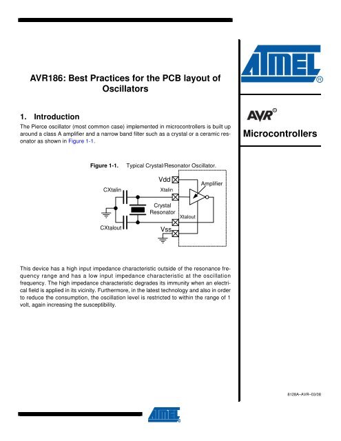
1. Introduction<br />
The Pierce oscillator (most common case) implemented in microcontrollers is built up<br />
around a class A amplifier and a narrow band filter such as a crystal or a ceramic resonator<br />
as shown in Figure 1-1.<br />
Figure 1-1. Typical Crystal/Resonator Oscillator.<br />
CXtalin<br />
CXtalout<br />
Vdd<br />
Xtalin<br />
Crystal<br />
Resonator<br />
Vss<br />
Xtalout<br />
Amplifier<br />
This device has a high input impedance characteristic outside <strong>of</strong> <strong>the</strong> resonance frequency<br />
range and has a low input impedance characteristic at <strong>the</strong> oscillation<br />
frequency. The high impedance characteristic degrades its immunity when an electrical<br />
field is applied in its vicinity. Fur<strong>the</strong>rmore, in <strong>the</strong> latest technology and also in order<br />
to reduce <strong>the</strong> consumption, <strong>the</strong> oscillation level is restricted to within <strong>the</strong> range <strong>of</strong> 1<br />
volt, again increasing <strong>the</strong> susceptibility.<br />
Microcontrollers<br />
8128A–AVR–03/08
2. Description<br />
2<br />
<strong>AVR186</strong><br />
In order to increase <strong>the</strong> robustness <strong>of</strong> this device against external disturbances, <strong>the</strong> design <strong>of</strong><br />
<strong>the</strong> <strong>PCB</strong> lay-out has to be done very carefully. An example is shown in Figure 2-1.<br />
Figure 2-1. Example <strong>of</strong> <strong>PCB</strong> <strong>layout</strong>.<br />
Crystal/Resonator<br />
CXtalin<br />
CXtalout<br />
Ground Plane<br />
Connection<br />
Local Ground<br />
plane<br />
Xtalin<br />
Xtalout<br />
Gnd<br />
8128A–AVR–03/08
3. Design Guidelines<br />
8128A–AVR–03/08<br />
<strong>AVR186</strong><br />
The following guidelines to design <strong>the</strong> <strong>layout</strong> are highly recommended in order not to risk failure<br />
and unstable oscillator operation.<br />
• The crystal and ceramic resonator oscillator is sensitive to stray capacitance and noise from<br />
o<strong>the</strong>r signals. It should be placed away from high frequency devices and traces in order to<br />
reduce <strong>the</strong> capacitive coupling between Xtal pins and <strong>PCB</strong> traces.<br />
• Keep o<strong>the</strong>r digital signal lines, especially clock lines and frequently switching signal lines, as<br />
far as away from <strong>the</strong> crystal connections as possible. Crosstalk from <strong>the</strong> digital activities may<br />
disturb <strong>the</strong> small-amplitude sine-shaped oscillator signal.<br />
• The ground connection <strong>for</strong> <strong>the</strong> load capacitors should be short and avoid <strong>the</strong> return currents<br />
from USB, RS232, LIN, PWM,… and power lines.<br />
• Load capacitors should be low leakage and stable across temperature (NPO or COG type).<br />
• The load capacitors should be placed close to each o<strong>the</strong>r.<br />
• The load Xtalin capacitor should be placed first and closest to <strong>the</strong> Xtalin pin and ground.<br />
• Parasitic capacitance will reduce gain margin. Keep this to an absolute minimum. For<br />
example typically:<br />
– Xtalin to ground : 1pF<br />
– Xtalout to ground : 2pF<br />
– Xtalin to Xtalout : 0.5pF<br />
These values are slightly package dependant.<br />
• Reduce <strong>the</strong> parasitic capacitance between Xtalin and Xtalout pins by routing <strong>the</strong>m as far<br />
apart as possible.<br />
• A ground area should be placed under <strong>the</strong> crystal oscillator area. This ground land should be<br />
connected to <strong>the</strong> oscillator ground.<br />
•<br />
• Connect <strong>the</strong> external capacitors needed <strong>for</strong> <strong>the</strong> crystal and <strong>the</strong> ceramic resonator operation<br />
as well as <strong>the</strong> crystal housing to <strong>the</strong> ground plane.<br />
• In case <strong>the</strong>re is only one <strong>PCB</strong> layer, it is recommended to place a guard ring around <strong>the</strong><br />
oscillator components and to connect it to <strong>the</strong> oscillator ground pin.<br />
3
Headquarters International<br />
Atmel Corporation<br />
2325 Orchard Parkway<br />
San Jose, CA 95131<br />
USA<br />
Tel: 1(408) 441-0311<br />
Fax: 1(408) 487-2600<br />
Atmel Asia<br />
Room 1219<br />
Chinachem Golden Plaza<br />
77 Mody Road Tsimshatsui<br />
East Kowloon<br />
Hong Kong<br />
Tel: (852) 2721-9778<br />
Fax: (852) 2722-1369<br />
Product Contact<br />
Web Site<br />
www.atmel.com<br />
Literature Requests<br />
www.atmel.com/literature<br />
Atmel Europe<br />
Le Krebs<br />
8, Rue Jean-Pierre Timbaud<br />
BP 309<br />
78054 Saint-Quentin-en-<br />
Yvelines Cedex<br />
France<br />
Tel: (33) 1-30-60-70-00<br />
Fax: (33) 1-30-60-71-11<br />
Technical Support<br />
AVR@atmel.com<br />
Atmel Japan<br />
9F, Tonetsu Shinkawa Bldg.<br />
1-24-8 Shinkawa<br />
Chuo-ku, Tokyo 104-0033<br />
Japan<br />
Tel: (81) 3-3523-3551<br />
Fax: (81) 3-3523-7581<br />
Sales Contact<br />
www.atmel.com/contacts<br />
Disclaimer: The in<strong>for</strong>mation in this document is provided in connection with Atmel products. No license, express or implied, by estoppel or o<strong>the</strong>rwise, to any<br />
intellectual property right is granted by this document or in connection with <strong>the</strong> sale <strong>of</strong> Atmel products. EXCEPT AS SET FORTH IN ATMEL’S TERMS AND CONDI-<br />
TIONS OF SALE LOCATED ON ATMEL’S WEB SITE, ATMEL ASSUMES NO LIABILITY WHATSOEVER AND DISCLAIMS ANY EXPRESS, IMPLIED OR STATUTORY<br />
WARRANTY RELATING TO ITS PRODUCTS INCLUDING, BUT NOT LIMITED TO, THE IMPLIED WARRANTY OF MERCHANTABILITY, FITNESS FOR A PARTICULAR<br />
PURPOSE, OR NON-INFRINGEMENT. IN NO EVENT SHALL ATMEL BE LIABLE FOR ANY DIRECT, INDIRECT, CONSEQUENTIAL, PUNITIVE, SPECIAL OR INCIDEN-<br />
TAL DAMAGES (INCLUDING, WITHOUT LIMITATION, DAMAGES FOR LOSS OF PROFITS, BUSINESS INTERRUPTION, OR LOSS OF INFORMATION) ARISING OUT<br />
OF THE USE OR INABILITY TO USE THIS DOCUMENT, EVEN IF ATMEL HAS BEEN ADVISED OF THE POSSIBILITY OF SUCH DAMAGES. Atmel makes no<br />
representations or warranties with respect to <strong>the</strong> accuracy or completeness <strong>of</strong> <strong>the</strong> contents <strong>of</strong> this document and reserves <strong>the</strong> right to make changes to specifications<br />
and product descriptions at any time without notice. Atmel does not make any commitment to update <strong>the</strong> in<strong>for</strong>mation contained herein. Unless specifically provided<br />
o<strong>the</strong>rwise, Atmel products are not suitable <strong>for</strong>, and shall not be used in, automotive applications. Atmel’s products are not intended, authorized, or warranted <strong>for</strong> use<br />
as components in applications intended to support or sustain life.<br />
© 2008 Atmel Corporation. All rights reserved. Atmel ® , logo and combinations <strong>the</strong>re<strong>of</strong>, and o<strong>the</strong>rs are registered trademarks or trademarks <strong>of</strong><br />
Atmel Corporation or its subsidiaries. O<strong>the</strong>r terms and product names may be trademarks <strong>of</strong> o<strong>the</strong>rs.<br />
8128A–AVR–03/08


