Computer-aided technique for defect and project rules inspection on ...
Computer-aided technique for defect and project rules inspection on ...
Computer-aided technique for defect and project rules inspection on ...

You also want an ePaper? Increase the reach of your titles
YUMPU automatically turns print PDFs into web optimized ePapers that Google loves.
<str<strong>on</strong>g>Computer</str<strong>on</strong>g>-<str<strong>on</strong>g>aided</str<strong>on</strong>g> <str<strong>on</strong>g>technique</str<strong>on</strong>g> <str<strong>on</strong>g>for</str<strong>on</strong>g> <str<strong>on</strong>g>defect</str<strong>on</strong>g> <str<strong>on</strong>g>and</str<strong>on</strong>g> <str<strong>on</strong>g>project</str<strong>on</strong>g> <str<strong>on</strong>g>rules</str<strong>on</strong>g> <str<strong>on</strong>g>inspecti<strong>on</strong></str<strong>on</strong>g> <strong>on</strong><br />
PCB layout image<br />
Alex<str<strong>on</strong>g>and</str<strong>on</strong>g>er Doudkin, Alex<str<strong>on</strong>g>and</str<strong>on</strong>g>er Inyutin<br />
United Institute of In<str<strong>on</strong>g>for</str<strong>on</strong>g>matics Problems, Nati<strong>on</strong>al Academy of Science of Belarus, 6 Surganov st.,<br />
Minsk, 220012, doudkin@newman.bas-net.by, avin@lsi.bas-net.by, tel.: (+375 17) 284 21 64<br />
Abstract: A <str<strong>on</strong>g>technique</str<strong>on</strong>g> of PCB layout optical <str<strong>on</strong>g>inspecti<strong>on</strong></str<strong>on</strong>g><br />
based <strong>on</strong> image comparis<strong>on</strong> <str<strong>on</strong>g>and</str<strong>on</strong>g> mathematical<br />
morphology methods is proposed. The unique feature of<br />
the <str<strong>on</strong>g>technique</str<strong>on</strong>g> is that the <str<strong>on</strong>g>inspecti<strong>on</strong></str<strong>on</strong>g> is per<str<strong>on</strong>g>for</str<strong>on</strong>g>med at<br />
different stages of image processing. The presence of all<br />
layout elements is checked up, then positi<strong>on</strong>s of found<br />
elements <str<strong>on</strong>g>and</str<strong>on</strong>g> their c<strong>on</strong><str<strong>on</strong>g>for</str<strong>on</strong>g>mity to <str<strong>on</strong>g>project</str<strong>on</strong>g> <str<strong>on</strong>g>rules</str<strong>on</strong>g> are<br />
verified, the breakouts <str<strong>on</strong>g>and</str<strong>on</strong>g> shorts are found. The<br />
<str<strong>on</strong>g>inspecti<strong>on</strong></str<strong>on</strong>g> of mousebits, spur <str<strong>on</strong>g>and</str<strong>on</strong>g> pinholes <strong>on</strong> c<strong>on</strong>ductors<br />
is also carried out.<br />
Keywords: PCB, layout <str<strong>on</strong>g>inspecti<strong>on</strong></str<strong>on</strong>g>, fault search <str<strong>on</strong>g>and</str<strong>on</strong>g><br />
classificati<strong>on</strong>.<br />
I. INTRODUCTION<br />
An important problem in manufacture of a<br />
microelectr<strong>on</strong>ic equipment is the printed circuit board<br />
(PCB) layout <str<strong>on</strong>g>inspecti<strong>on</strong></str<strong>on</strong>g>. The n<strong>on</strong>-c<strong>on</strong>tact optical methods<br />
is widely used the c<strong>on</strong>trol of PCBs.<br />
An object <str<strong>on</strong>g>for</str<strong>on</strong>g> the <str<strong>on</strong>g>inspecti<strong>on</strong></str<strong>on</strong>g> will be the image of PCB<br />
layout. The problem definiti<strong>on</strong> is the following. The raster<br />
pattern of the PCB layout <str<strong>on</strong>g>and</str<strong>on</strong>g> the set of <str<strong>on</strong>g>project</str<strong>on</strong>g> <str<strong>on</strong>g>rules</str<strong>on</strong>g> are<br />
given. The artwork image of PCB layoutcan be given in<br />
additi<strong>on</strong>. It is required to check whether the PCB elements<br />
meet the given <str<strong>on</strong>g>project</str<strong>on</strong>g> <str<strong>on</strong>g>rules</str<strong>on</strong>g>, <str<strong>on</strong>g>and</str<strong>on</strong>g> to described their<br />
<str<strong>on</strong>g>defect</str<strong>on</strong>g>s.<br />
As elements <strong>on</strong> the PCB layout image we will define the<br />
c<strong>on</strong>tact pads, c<strong>on</strong>ductors, c<strong>on</strong>trol points <str<strong>on</strong>g>and</str<strong>on</strong>g> the service<br />
in<str<strong>on</strong>g>for</str<strong>on</strong>g>mati<strong>on</strong> in the character <str<strong>on</strong>g>for</str<strong>on</strong>g>m. The <str<strong>on</strong>g>defect</str<strong>on</strong>g> under<br />
<str<strong>on</strong>g>inspecti<strong>on</strong></str<strong>on</strong>g> is the deviati<strong>on</strong> of layout elements <strong>on</strong> PCB<br />
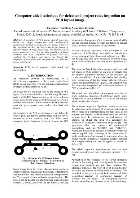
Fig. 1 - Example of a PCB layout <str<strong>on</strong>g>defect</str<strong>on</strong>g>s:<br />
1) spurious copper; 2) spur; 3) mousebit; 4) pin<br />
hole; 5)short; 6) breakout.<br />
layout image from the <str<strong>on</strong>g>project</str<strong>on</strong>g> documentati<strong>on</strong> owing to<br />
errors by manufacture, such as discrepancy of temperature<br />
<str<strong>on</strong>g>and</str<strong>on</strong>g> manufacture time modes, mechanical misregistrati<strong>on</strong>,<br />
etc. The example of some <str<strong>on</strong>g>defect</str<strong>on</strong>g>s is replaced <strong>on</strong> fig.1. The<br />
<str<strong>on</strong>g>defect</str<strong>on</strong>g>s can be divided into the following kinds: spurious<br />
copper (1), spur (2), mousebit (3), pin hole (4), short (5),<br />
breakout (6), discrepancy of the c<strong>on</strong>ductor minimal width<br />
<str<strong>on</strong>g>and</str<strong>on</strong>g> the minimal distance between c<strong>on</strong>ductors to <str<strong>on</strong>g>project</str<strong>on</strong>g><br />
<str<strong>on</strong>g>rules</str<strong>on</strong>g>, absence or displacement of any element [1].<br />
Various automatic algorithms were developed to the<br />
<str<strong>on</strong>g>inspecti<strong>on</strong></str<strong>on</strong>g> of PCB layout over different manufacture<br />
phases with use of light, fluorescent light <str<strong>on</strong>g>and</str<strong>on</strong>g> x-ray. They<br />
can be separeted into three categories: reference based,<br />
<str<strong>on</strong>g>project</str<strong>on</strong>g> <str<strong>on</strong>g>rules</str<strong>on</strong>g> verificati<strong>on</strong> based <str<strong>on</strong>g>and</str<strong>on</strong>g> hybrid algorithms [1-<br />
4].<br />
The reference based algorithms compare reference <str<strong>on</strong>g>and</str<strong>on</strong>g><br />
test images of PCBs directly or use a set of models with<br />
the advance in<str<strong>on</strong>g>for</str<strong>on</strong>g>mative attributes as the reference. At<br />
comparis<strong>on</strong> with the reference it is possible both pixel by<br />
pixel comparis<strong>on</strong> of the test image with the reference<br />
sample image (subtracti<strong>on</strong> of images), <str<strong>on</strong>g>and</str<strong>on</strong>g> allocati<strong>on</strong> with<br />
the subsequent comparis<strong>on</strong> of in<str<strong>on</strong>g>for</str<strong>on</strong>g>mati<strong>on</strong> attributes of<br />
PCB layout elements [1, 5 - 7]<br />
The model based algorithms, such as parse, algorithm of<br />
graph matching, algorithm of attributed graphs make<br />
comparis<strong>on</strong> of layout elements as a set of the models<br />
which describe the reference.<br />
The automatic <str<strong>on</strong>g>inspecti<strong>on</strong></str<strong>on</strong>g> algorithms, which are not use<br />
the reference, check elements of layout <strong>on</strong> c<strong>on</strong><str<strong>on</strong>g>for</str<strong>on</strong>g>mity to<br />
<str<strong>on</strong>g>project</str<strong>on</strong>g> <str<strong>on</strong>g>rules</str<strong>on</strong>g> of a microelectr<strong>on</strong>ic product, such as the<br />
minimal <str<strong>on</strong>g>and</str<strong>on</strong>g> maximal width of c<strong>on</strong>ductors <str<strong>on</strong>g>and</str<strong>on</strong>g> distance<br />
between them, the minimal <str<strong>on</strong>g>and</str<strong>on</strong>g> maximal diameter of<br />
apertures <strong>on</strong> object, the curve of a c<strong>on</strong>ductor, the<br />
<str<strong>on</strong>g>inspecti<strong>on</strong></str<strong>on</strong>g> of c<strong>on</strong>ductors terminati<strong>on</strong> <str<strong>on</strong>g>rules</str<strong>on</strong>g>, etc [8]. That<br />
algorithms often use operators of mathematical<br />
morphology, such as “ERODE” <str<strong>on</strong>g>and</str<strong>on</strong>g> “DILATE”.<br />
Algorithms based <strong>on</strong> the analysis of elements border can<br />
also be applied. After obtaining of the border there is<br />
made verificati<strong>on</strong> of an element by movement al<strong>on</strong>g its<br />
border with the <str<strong>on</strong>g>inspecti<strong>on</strong></str<strong>on</strong>g> of special parameters. Element<br />
edge lengths coding can also be applied to search of<br />
<str<strong>on</strong>g>defect</str<strong>on</strong>g>s [1].<br />
The hybrid <str<strong>on</strong>g>inspecti<strong>on</strong></str<strong>on</strong>g> algorithms are based <strong>on</strong> both<br />
comparis<strong>on</strong> <str<strong>on</strong>g>and</str<strong>on</strong>g> <str<strong>on</strong>g>project</str<strong>on</strong>g> <str<strong>on</strong>g>rules</str<strong>on</strong>g> verificati<strong>on</strong> methods [1, 9 -<br />
11].<br />
Applicati<strong>on</strong> of the reference <str<strong>on</strong>g>for</str<strong>on</strong>g> the layout <str<strong>on</strong>g>inspecti<strong>on</strong></str<strong>on</strong>g><br />
allows to find quickly <str<strong>on</strong>g>and</str<strong>on</strong>g> correctly faults like spurious<br />
copper, spur, mousebit, pin hole, short, breakout. The<br />
additi<strong>on</strong>al analysis of the received set of the faults allow<br />
us to find the absence or displacement of elements. The<br />
main lack of the given approach is dependence of faults<br />
localizati<strong>on</strong> accuracy <strong>on</strong> overlapping accuracy of<br />
reference <str<strong>on</strong>g>and</str<strong>on</strong>g> test images. The overlapping accuracy<br />
depends <strong>on</strong> scaling <str<strong>on</strong>g>and</str<strong>on</strong>g> turn operati<strong>on</strong>s of the test image,
its preliminary processing <str<strong>on</strong>g>and</str<strong>on</strong>g> binarizati<strong>on</strong>. For the<br />
<str<strong>on</strong>g>inspecti<strong>on</strong></str<strong>on</strong>g> of the minimal c<strong>on</strong>ductor width <str<strong>on</strong>g>and</str<strong>on</strong>g> the<br />
minimal distance between c<strong>on</strong>ductors we shall use the<br />
algorithm based <strong>on</strong> morphological operators “OPEN” <str<strong>on</strong>g>and</str<strong>on</strong>g><br />
“CLOSE”.<br />
In the paper we offer new <str<strong>on</strong>g>technique</str<strong>on</strong>g> of PCB <str<strong>on</strong>g>inspecti<strong>on</strong></str<strong>on</strong>g><br />
with using advantages of the image comparis<strong>on</strong> approach<br />
<str<strong>on</strong>g>and</str<strong>on</strong>g> the method based <strong>on</strong> mathematical morphology<br />
operators. The PCB layout <str<strong>on</strong>g>inspecti<strong>on</strong></str<strong>on</strong>g> <str<strong>on</strong>g>technique</str<strong>on</strong>g><br />
represents stage-by-stage procedure. In the beginning<br />
preliminary image processing is made. The presence of all<br />
elements <strong>on</strong> the PCB layout image is checked up at this<br />
stage. The output of this stage is the binary PCB layout<br />
image with corrected scale <str<strong>on</strong>g>and</str<strong>on</strong>g> rotati<strong>on</strong> angle. At the next<br />
stage the search of <str<strong>on</strong>g>defect</str<strong>on</strong>g>s is per<str<strong>on</strong>g>for</str<strong>on</strong>g>med using method of<br />
comparis<strong>on</strong> with the reference. The search can be carried<br />
out <strong>on</strong> the raster image or <strong>on</strong> its vector representati<strong>on</strong>.<br />
The found <str<strong>on</strong>g>defect</str<strong>on</strong>g>s are classified <str<strong>on</strong>g>and</str<strong>on</strong>g> their geometrical<br />
parameters are measured. At the last stage the search of<br />
<str<strong>on</strong>g>defect</str<strong>on</strong>g>s with use of morphological operators "OPEN" <str<strong>on</strong>g>and</str<strong>on</strong>g><br />
"CLOSE" is per<str<strong>on</strong>g>for</str<strong>on</strong>g>med. There<str<strong>on</strong>g>for</str<strong>on</strong>g>e we define regi<strong>on</strong>s <strong>on</strong><br />
the PCB layout image, where <str<strong>on</strong>g>project</str<strong>on</strong>g> <str<strong>on</strong>g>rules</str<strong>on</strong>g> <str<strong>on</strong>g>for</str<strong>on</strong>g> the<br />
minimal width of a c<strong>on</strong>ductor <str<strong>on</strong>g>and</str<strong>on</strong>g> the minimal distance<br />
between c<strong>on</strong>ductors are not carried out.<br />
The paper is organized as follows. In secti<strong>on</strong> 2 the<br />
<str<strong>on</strong>g>technique</str<strong>on</strong>g> of the <str<strong>on</strong>g>defect</str<strong>on</strong>g>s search based <strong>on</strong> a method of<br />
comparis<strong>on</strong> with the reference is offered. The search of<br />
layout <str<strong>on</strong>g>defect</str<strong>on</strong>g>s is realized both <str<strong>on</strong>g>for</str<strong>on</strong>g> raster, <str<strong>on</strong>g>and</str<strong>on</strong>g> <str<strong>on</strong>g>for</str<strong>on</strong>g> vector<br />
representati<strong>on</strong> of the PCB layout image. The method of<br />
classificati<strong>on</strong> of <str<strong>on</strong>g>defect</str<strong>on</strong>g>s is offered. The technology of<br />
search of <str<strong>on</strong>g>defect</str<strong>on</strong>g>s like a deviati<strong>on</strong> of the minimal width of<br />
a c<strong>on</strong>ductor <str<strong>on</strong>g>and</str<strong>on</strong>g> the minimal distance between c<strong>on</strong>ductors<br />
from <str<strong>on</strong>g>project</str<strong>on</strong>g> <str<strong>on</strong>g>rules</str<strong>on</strong>g> is also c<strong>on</strong>sidered.<br />
II. DESCRIPTION OF THE TECHNIQUE<br />
OF PCB LAYOUT INSPECTION<br />
A. Preliminary image processing<br />
Preliminary processing of the test image c<strong>on</strong>sists of<br />
binarizati<strong>on</strong>, correcti<strong>on</strong>s of a rotati<strong>on</strong> angle <str<strong>on</strong>g>and</str<strong>on</strong>g> scaling.<br />
The gray-scale picture received from an optical system is<br />
trans<str<strong>on</strong>g>for</str<strong>on</strong>g>med to a binary image using the treshold Bts<br />
calculeted by the <str<strong>on</strong>g>for</str<strong>on</strong>g>mula:<br />
Bts = 2/3 * (Bmax - Bmin), (1)<br />
where Bmax <str<strong>on</strong>g>and</str<strong>on</strong>g> Bmin are the maximal <str<strong>on</strong>g>and</str<strong>on</strong>g> minimal<br />
values of brightness of the image.<br />
The test image can have distorti<strong>on</strong>s of scale <str<strong>on</strong>g>and</str<strong>on</strong>g> a rotati<strong>on</strong><br />
angle. C<strong>on</strong>trol points are used To correct these distorti<strong>on</strong>s.<br />
The c<strong>on</strong>trol points are selected <strong>on</strong> the reference image,<br />
<str<strong>on</strong>g>and</str<strong>on</strong>g> then the search of these points is per<str<strong>on</strong>g>for</str<strong>on</strong>g>med <strong>on</strong> the<br />
test image. Finally the correcti<strong>on</strong> of the rotati<strong>on</strong> angle <str<strong>on</strong>g>and</str<strong>on</strong>g><br />
scale is carried out.<br />
Search of all c<strong>on</strong>tact pads is made <strong>on</strong> the binary image,<br />
<str<strong>on</strong>g>and</str<strong>on</strong>g> lists of c<strong>on</strong>tact pads <str<strong>on</strong>g>for</str<strong>on</strong>g> the reference <str<strong>on</strong>g>and</str<strong>on</strong>g> test image<br />
are <str<strong>on</strong>g>for</str<strong>on</strong>g>med accordingly. The reference <str<strong>on</strong>g>and</str<strong>on</strong>g> test lists are<br />
compared with each other, there<str<strong>on</strong>g>for</str<strong>on</strong>g>e presence of all<br />
elements <strong>on</strong> the PCB layout image is checked up, <str<strong>on</strong>g>and</str<strong>on</strong>g><br />
finally verificati<strong>on</strong> of found elements positi<strong>on</strong> is<br />
per<str<strong>on</strong>g>for</str<strong>on</strong>g>med.<br />
2<br />
7<br />
1<br />
6<br />
1<br />
B. The PCB layout <str<strong>on</strong>g>inspecti<strong>on</strong></str<strong>on</strong>g><br />
After the preliminary processing the search of <str<strong>on</strong>g>defect</str<strong>on</strong>g>s by<br />
a method of pixel by pixel calculati<strong>on</strong>s of XOR logic<br />
operati<strong>on</strong> <strong>on</strong> reference <str<strong>on</strong>g>and</str<strong>on</strong>g> test images is carried out.<br />
It is necessary to carry out the following tasks:<br />
a)<br />
b)<br />
4<br />
c)<br />
1 1<br />
Fig. 2 - The reference PCB layout image (a); processing<br />
image (b); found <str<strong>on</strong>g>defect</str<strong>on</strong>g>s (c): 1) spur, 2) spurious<br />
copper, 3) short, 4) mousebit, 5) pin hole, 6) breakout,<br />
7) distance between c<strong>on</strong>ductors is less than <str<strong>on</strong>g>project</str<strong>on</strong>g><br />
<str<strong>on</strong>g>rules</str<strong>on</strong>g>, 8) the width of a c<strong>on</strong>ductor is less than <str<strong>on</strong>g>project</str<strong>on</strong>g><br />
<str<strong>on</strong>g>rules</str<strong>on</strong>g>.<br />
1. Find faults of the PCB by comparis<strong>on</strong> a binary<br />
reference <str<strong>on</strong>g>and</str<strong>on</strong>g> test images.<br />
4<br />
5<br />
3<br />
8
2. Measure geometrical parameters of <str<strong>on</strong>g>defect</str<strong>on</strong>g> are: length,<br />
height <str<strong>on</strong>g>and</str<strong>on</strong>g> the area.<br />
3. Classify faults as:<br />
− spurious copper;<br />
− spur;<br />
− mousebit;<br />
− pin hole;<br />
− short;<br />
− breakout<br />
The vector descripti<strong>on</strong> is made <str<strong>on</strong>g>for</str<strong>on</strong>g> each <str<strong>on</strong>g>defect</str<strong>on</strong>g>. On fig.2.a<br />
example of the reference PCB layout image are depicted.<br />
On fig.2.b <strong>on</strong>e can see its image with <str<strong>on</strong>g>defect</str<strong>on</strong>g>s <str<strong>on</strong>g>and</str<strong>on</strong>g> the<br />
de<str<strong>on</strong>g>for</str<strong>on</strong>g>med scale <str<strong>on</strong>g>and</str<strong>on</strong>g> the rotati<strong>on</strong> angle. The result of<br />
<str<strong>on</strong>g>defect</str<strong>on</strong>g>s search by means of operati<strong>on</strong> XOR is shown <strong>on</strong><br />
fig.2.c (<str<strong>on</strong>g>defect</str<strong>on</strong>g>s are marked by numbers 1 - 6).<br />
C. The <str<strong>on</strong>g>inspecti<strong>on</strong></str<strong>on</strong>g> <strong>on</strong> the vector image of PCB layout<br />
Search of faults like spur <str<strong>on</strong>g>and</str<strong>on</strong>g> mousebit <strong>on</strong> vector<br />
representati<strong>on</strong> of the image of the PCB is realized <strong>on</strong> the<br />
basis of algorithms Weiler-Athert<strong>on</strong> <str<strong>on</strong>g>and</str<strong>on</strong>g> Margalit-Knott.<br />
For search of faults vector representati<strong>on</strong>s of reference<br />
<str<strong>on</strong>g>and</str<strong>on</strong>g> test images of PCB are used.<br />
All elements <strong>on</strong> the image of the PCB are c<strong>on</strong>sidered as<br />
polyg<strong>on</strong>s. First, a check of an intersecti<strong>on</strong> of reference<br />
<str<strong>on</strong>g>and</str<strong>on</strong>g> test polyg<strong>on</strong>s by the coordinates <strong>on</strong> the image is<br />
per<str<strong>on</strong>g>for</str<strong>on</strong>g>med. If polyg<strong>on</strong>s are intersected, points of mutual<br />
crossing of the polyg<strong>on</strong>s borders are calculated <str<strong>on</strong>g>and</str<strong>on</strong>g> then<br />
tracing al<strong>on</strong>g borders of polyg<strong>on</strong>s is carried out <str<strong>on</strong>g>for</str<strong>on</strong>g><br />
building of a required polyg<strong>on</strong>. Tracing begins from an<br />
external point of local area of polyg<strong>on</strong>s. After the first<br />
point of edge crossing is reached, tracing is carried out <strong>on</strong><br />
the internal side of the polyg<strong>on</strong> <str<strong>on</strong>g>for</str<strong>on</strong>g>med by crossing of the<br />
edges of c<strong>on</strong>sidered polyg<strong>on</strong>s in an opposite to initial <strong>on</strong>e<br />
directi<strong>on</strong>. After the sec<strong>on</strong>d point of the polyg<strong>on</strong>s edges<br />
crossing is reached, procedure returns to the starting point<br />
of tracing <strong>on</strong> the external edge of a new polyg<strong>on</strong>. Having<br />
defined thus coordinates of all points of a new polyg<strong>on</strong>,<br />
we obtain vector representati<strong>on</strong> of PCB <str<strong>on</strong>g>defect</str<strong>on</strong>g>.<br />
Then the vector descripti<strong>on</strong> of all found <str<strong>on</strong>g>defect</str<strong>on</strong>g>s of the<br />
PCB is made.<br />
D. The <str<strong>on</strong>g>defect</str<strong>on</strong>g> classificati<strong>on</strong><br />
After <str<strong>on</strong>g>defect</str<strong>on</strong>g> localizati<strong>on</strong> we determine which class of<br />
faults it bel<strong>on</strong>gs to. Classificati<strong>on</strong> is realized by means of<br />
the logical flags defining value of brightness <str<strong>on</strong>g>for</str<strong>on</strong>g> pixels of<br />
the found fault <str<strong>on</strong>g>and</str<strong>on</strong>g> the pixels around it. In table 1 the<br />
<str<strong>on</strong>g>rules</str<strong>on</strong>g> of classificati<strong>on</strong> is shown dependinging <strong>on</strong> various<br />
values of flags.<br />
Let's c<strong>on</strong>sider the example of the <str<strong>on</strong>g>defect</str<strong>on</strong>g> <strong>on</strong> fig.3, where<br />
figure fragments of two direct c<strong>on</strong>ductors are represented.<br />
To each pixel <strong>on</strong> the image there corresp<strong>on</strong>ds as square.<br />
Pixels corresp<strong>on</strong>ding to c<strong>on</strong>ductors <strong>on</strong> the reference<br />
image are shown by grey color. C<strong>on</strong>ductors are marked<br />
by numbers in the left top corner. The background is<br />
presented by white pixels. Pixels of <str<strong>on</strong>g>defect</str<strong>on</strong>g> have black<br />
color <str<strong>on</strong>g>and</str<strong>on</strong>g> are marked by small white squares. Pixels<br />
which border <strong>on</strong> <str<strong>on</strong>g>defect</str<strong>on</strong>g>, are marked by diag<strong>on</strong>al lines. It<br />
Fig. 3 - The <str<strong>on</strong>g>defect</str<strong>on</strong>g> classificati<strong>on</strong>: a) reference image, b) test image with <str<strong>on</strong>g>defect</str<strong>on</strong>g>.<br />
Table 1. Fault type definiti<strong>on</strong> by logical flags<br />
Is there the<br />
<str<strong>on</strong>g>defect</str<strong>on</strong>g> copper<br />
<strong>on</strong><br />
background?<br />
a) b)<br />
Does the <str<strong>on</strong>g>defect</str<strong>on</strong>g><br />
touch with<br />
copper?<br />
Logical flag<br />
Does the <str<strong>on</strong>g>defect</str<strong>on</strong>g><br />
touch with<br />
background?<br />
Does the <str<strong>on</strong>g>defect</str<strong>on</strong>g><br />
touch <strong>on</strong>ly <strong>on</strong>e<br />
c<strong>on</strong>ductor?<br />
- background<br />
pixel<br />
- pixel of<br />
c<strong>on</strong>ductor <strong>on</strong><br />
reference<br />
image<br />
- c<strong>on</strong>ductor’s<br />
pixel near to<br />
<str<strong>on</strong>g>defect</str<strong>on</strong>g><br />
- <str<strong>on</strong>g>defect</str<strong>on</strong>g> pixel<br />
- background<br />
pixel near to<br />
<str<strong>on</strong>g>defect</str<strong>on</strong>g><br />
Type of <str<strong>on</strong>g>defect</str<strong>on</strong>g><br />
Yes Yes Yes Yes Spur<br />
Yes Yes Yes No Short<br />
Yes No No Yes Spurious copper<br />
No Yes No Yes Pin hole<br />
No Yes Yes Yes Mousebit<br />
No Yes Yes No Breakout
can be seen that:<br />
<str<strong>on</strong>g>defect</str<strong>on</strong>g> looks like a set of black pixels <strong>on</strong> a white<br />
background;<br />
<str<strong>on</strong>g>defect</str<strong>on</strong>g> is adjoined with both black <str<strong>on</strong>g>and</str<strong>on</strong>g> white pixels of<br />
the image;<br />
<str<strong>on</strong>g>defect</str<strong>on</strong>g> adjoins <strong>on</strong>ly to <strong>on</strong>e element <strong>on</strong> the image<br />
(element 1).<br />
According to table 1 the <str<strong>on</strong>g>defect</str<strong>on</strong>g> is classified as spur.<br />
For faults like spur <str<strong>on</strong>g>and</str<strong>on</strong>g> mousebit the additi<strong>on</strong>al check is<br />
made: if the fault borders <strong>on</strong> two or more PCB elements<br />
<strong>on</strong> initial images, it bel<strong>on</strong>g to the class of short <str<strong>on</strong>g>and</str<strong>on</strong>g><br />
breakout accordingly.<br />
E. The <str<strong>on</strong>g>inspecti<strong>on</strong></str<strong>on</strong>g> the minimal c<strong>on</strong>ductor width <str<strong>on</strong>g>and</str<strong>on</strong>g> the<br />
minimal distance between c<strong>on</strong>ductors<br />
At the certain PCB manufacturing phase there is a<br />
necessity to check c<strong>on</strong><str<strong>on</strong>g>for</str<strong>on</strong>g>mity of the minimal width of a<br />
c<strong>on</strong>ductor <str<strong>on</strong>g>and</str<strong>on</strong>g> the minimal distance between c<strong>on</strong>ductors<br />
to <str<strong>on</strong>g>project</str<strong>on</strong>g> <str<strong>on</strong>g>rules</str<strong>on</strong>g>. Localizati<strong>on</strong> of points <strong>on</strong> the image,<br />
where these <str<strong>on</strong>g>project</str<strong>on</strong>g> <str<strong>on</strong>g>rules</str<strong>on</strong>g> do not carry out, is made with<br />
use of mathematical morphology operators “OPEN” <str<strong>on</strong>g>and</str<strong>on</strong>g><br />
“CLOSE” [12]. To define c<strong>on</strong>ductor regi<strong>on</strong>s with a width<br />
less than set <str<strong>on</strong>g>project</str<strong>on</strong>g> <str<strong>on</strong>g>rules</str<strong>on</strong>g>, the next <str<strong>on</strong>g>for</str<strong>on</strong>g>mula is used:<br />
Rminwide (A, B) = A - OPEN (A, B), (2)<br />
where A is the binary test image of the PCB, B is the<br />
round structuring element, which diameter is equal to the<br />
minimal width of the c<strong>on</strong>ductor according to <str<strong>on</strong>g>project</str<strong>on</strong>g> <str<strong>on</strong>g>rules</str<strong>on</strong>g>.<br />
Morphological operati<strong>on</strong> “OPEN” has a property to delete<br />
those regi<strong>on</strong>s, which width is less than the structuring<br />
element. The result of the given operati<strong>on</strong> is the set of<br />
image regi<strong>on</strong>s with width of a c<strong>on</strong>ductor less then<br />
minimal admissible <strong>on</strong> <str<strong>on</strong>g>project</str<strong>on</strong>g> <str<strong>on</strong>g>rules</str<strong>on</strong>g>.<br />
For receiving of test image regi<strong>on</strong>s with the distance<br />
between c<strong>on</strong>ductors less then <str<strong>on</strong>g>project</str<strong>on</strong>g> <str<strong>on</strong>g>rules</str<strong>on</strong>g> we use the<br />
<str<strong>on</strong>g>for</str<strong>on</strong>g>mula<br />
Rmindist (A,C) = A - CLOSE (A,C) (3)<br />
where A are the binary test image of the PCB, C are the<br />
round structuring element, which diameter is equal to the<br />
minimal distance between c<strong>on</strong>ductors according to <str<strong>on</strong>g>project</str<strong>on</strong>g><br />
<str<strong>on</strong>g>rules</str<strong>on</strong>g>. Morphological operati<strong>on</strong> “CLOSE” has a property<br />
to delete those spaces <strong>on</strong> images, which width less than a<br />
structuring element. The result of the operati<strong>on</strong> is a set of<br />
image regi<strong>on</strong>s with distance between c<strong>on</strong>ductors less then<br />
minimal admissible <strong>on</strong> <str<strong>on</strong>g>project</str<strong>on</strong>g> <str<strong>on</strong>g>rules</str<strong>on</strong>g>.<br />
The example of the <str<strong>on</strong>g>defect</str<strong>on</strong>g>s caused by discrepancy is<br />
<str<strong>on</strong>g>project</str<strong>on</strong>g> <str<strong>on</strong>g>rules</str<strong>on</strong>g> is shown <strong>on</strong> fig. 2.c: number 7 marks <str<strong>on</strong>g>defect</str<strong>on</strong>g><br />
like distance between c<strong>on</strong>ductors having width less than<br />
<str<strong>on</strong>g>project</str<strong>on</strong>g> <str<strong>on</strong>g>rules</str<strong>on</strong>g> <str<strong>on</strong>g>and</str<strong>on</strong>g> number 8 marks <str<strong>on</strong>g>defect</str<strong>on</strong>g> like the<br />
c<strong>on</strong>ductors width is less than <str<strong>on</strong>g>project</str<strong>on</strong>g> <str<strong>on</strong>g>rules</str<strong>on</strong>g>.<br />
III. CONCLUSION<br />
Technique of PCB layout <str<strong>on</strong>g>inspecti<strong>on</strong></str<strong>on</strong>g> based <strong>on</strong> image<br />
comparis<strong>on</strong> <str<strong>on</strong>g>and</str<strong>on</strong>g> mathematical morphology methods is<br />
offered. The method of classificati<strong>on</strong> of <str<strong>on</strong>g>defect</str<strong>on</strong>g>s <strong>on</strong> the<br />
basis of logycal flags is offered. As a result there will be<br />
checked up the presence of all elements <strong>on</strong> the PCB,<br />
verificati<strong>on</strong> of found elements positi<strong>on</strong> <str<strong>on</strong>g>and</str<strong>on</strong>g> their<br />
c<strong>on</strong><str<strong>on</strong>g>for</str<strong>on</strong>g>mity to <str<strong>on</strong>g>project</str<strong>on</strong>g> <str<strong>on</strong>g>rules</str<strong>on</strong>g>, the presence of breakouts <str<strong>on</strong>g>and</str<strong>on</strong>g><br />
shorts <strong>on</strong> the PCB. The <str<strong>on</strong>g>inspecti<strong>on</strong></str<strong>on</strong>g> of mousebits, spur <str<strong>on</strong>g>and</str<strong>on</strong>g><br />
pinholes <strong>on</strong> c<strong>on</strong>ductors is also carried out.<br />
The proposed <str<strong>on</strong>g>technique</str<strong>on</strong>g> is realized in the computer-<str<strong>on</strong>g>aided</str<strong>on</strong>g><br />
system of the PCB layout <str<strong>on</strong>g>inspecti<strong>on</strong></str<strong>on</strong>g>. The PCB layout<br />
<str<strong>on</strong>g>inspecti<strong>on</strong></str<strong>on</strong>g> system allows carrying out automatic<br />
<str<strong>on</strong>g>inspecti<strong>on</strong></str<strong>on</strong>g> of c<strong>on</strong><str<strong>on</strong>g>for</str<strong>on</strong>g>mity c<strong>on</strong>tact pads <strong>on</strong> the tested PCB<br />
(<strong>on</strong> types <str<strong>on</strong>g>and</str<strong>on</strong>g> an arrangement) to data in Gerber <str<strong>on</strong>g>for</str<strong>on</strong>g>mat of<br />
the reference PCB. Automatic <str<strong>on</strong>g>inspecti<strong>on</strong></str<strong>on</strong>g> of c<strong>on</strong>ductors<br />
faults. The system is realized under OS Linux in the<br />
programming language C++.<br />
REFERENCES<br />
[1] M. Moganti, F. Ercal, C. Dagli, S. Tsunekawa.<br />
Automatic PCI Inspecti<strong>on</strong> Algorithms: A Survey,<br />
<str<strong>on</strong>g>Computer</str<strong>on</strong>g> Visi<strong>on</strong> <str<strong>on</strong>g>and</str<strong>on</strong>g> Image Underst<str<strong>on</strong>g>and</str<strong>on</strong>g>ing 63 (1996),<br />
287-313.<br />
[2] Tom Lecklider. PCB Inspecti<strong>on</strong> Outlook <str<strong>on</strong>g>for</str<strong>on</strong>g> 2005.<br />
www.evaluati<strong>on</strong>engineering.com/archive/articles/1204/12<br />
04pcb_<str<strong>on</strong>g>inspecti<strong>on</strong></str<strong>on</strong>g>.asp<br />
[3] Elias N. Malamas, Euripides G. M. Petrakis,<br />
Michalis Zervakis, Laurent Petit, Jean-Didier Legat. A<br />
survey <strong>on</strong> industrial visi<strong>on</strong> systems, applicati<strong>on</strong>s, tools.<br />
Image Visi<strong>on</strong> Computing 2003, Vol. 21, Issue 2, p. 171 -<br />
188<br />
[4] K. C. Fan, C. Hsu. Strategic planning of developing<br />
automatic optical <str<strong>on</strong>g>inspecti<strong>on</strong></str<strong>on</strong>g> (AOI) technologies in<br />
Taiwan, J. Phys.: C<strong>on</strong>f. 2005 Ser. 13 394-397<br />
[5] Efrat Tal, Inbal Yefet. Printed Circuit Board<br />
Inspecti<strong>on</strong>. http://visl.techni<strong>on</strong>.ac.il/<str<strong>on</strong>g>project</str<strong>on</strong>g>s/2002w23/<br />
[6] Zuwairie Ibrahim <str<strong>on</strong>g>and</str<strong>on</strong>g> Syed Abd. Rahman Al-Attas.<br />
Wavelet-Based Printed Circuit Board Inspecti<strong>on</strong> System,<br />
Internati<strong>on</strong>al Journal of Signal Processing (IJSP), 1,<br />
2004, pp. 65-71.<br />
[7] N. -H. Kim, J. -Y. Pyun, K. -S. Choi, B. -D. Choi,<br />
<str<strong>on</strong>g>and</str<strong>on</strong>g> S. -J. Ko, "Real-Time Inspecti<strong>on</strong> System For Printed<br />
Circuit Boards," Proc. of 2001 IEEE Internati<strong>on</strong>al.<br />
Symposium <strong>on</strong> Industrial electr<strong>on</strong>ics Proceedings, vol. 1,<br />
pp. 166-170, Pusan, Korea , Jul. 2001.<br />
[8] P. Szolgay, K. Tömördi, “Analogic algorithms <str<strong>on</strong>g>for</str<strong>on</strong>g><br />
optical detecti<strong>on</strong> of breaks <str<strong>on</strong>g>and</str<strong>on</strong>g> short circuits <strong>on</strong> the<br />
layouts of printed circuit boards using CNN”<br />
Internati<strong>on</strong>al Journal of Circuit Theory <str<strong>on</strong>g>and</str<strong>on</strong>g> Applicati<strong>on</strong>s<br />
27, pp. 103-116, 1999<br />
[9] T. Hidvégi, P. Szolgay: Some new analogic CNN<br />
algorithms <str<strong>on</strong>g>for</str<strong>on</strong>g> PCB quality c<strong>on</strong>trol, Int. J. of Circuit<br />
Theory <str<strong>on</strong>g>and</str<strong>on</strong>g> Applicati<strong>on</strong>s, Vol. 30, pp. 231-245, 2002<br />
[10] M. Moganti <str<strong>on</strong>g>and</str<strong>on</strong>g> F. Ercal, "Sub-Pattern Level<br />
Inspecti<strong>on</strong> System <str<strong>on</strong>g>for</str<strong>on</strong>g> Printed Circuit Boards," <str<strong>on</strong>g>Computer</str<strong>on</strong>g><br />
Visi<strong>on</strong> <str<strong>on</strong>g>and</str<strong>on</strong>g> Image Underst<str<strong>on</strong>g>and</str<strong>on</strong>g>ing, Vol. 70, No. 1, pp. 51-<br />
62, April 1998.<br />
[11] M. Moganti <str<strong>on</strong>g>and</str<strong>on</strong>g> F. Ercal, "Segmentati<strong>on</strong> of<br />
Printed Circuit Board Images into Basic Patterns ,"<br />
<str<strong>on</strong>g>Computer</str<strong>on</strong>g> Visi<strong>on</strong> <str<strong>on</strong>g>and</str<strong>on</strong>g> Image Underst<str<strong>on</strong>g>and</str<strong>on</strong>g>ing, Vol. 70, No.<br />
1, pp. 74-86, April 1998.<br />
[12] Dougherty E.R. An introducti<strong>on</strong> to morphological<br />
image processing, Bellingham, Washingt<strong>on</strong>, 1992.<br />
The research is partially supported by the Belarusian<br />
Republican Foundati<strong>on</strong> of Fundamental Research, grants<br />
T04-219 <str<strong>on</strong>g>and</str<strong>on</strong>g> T04M-119.