- Page 1:
Operational Amplifier Chapter 1: Th
- Page 4 and 5:
1-2 problem. It seems that circuits
- Page 6 and 7:
1-4 you are looking in the wrong pl
- Page 8 and 9:
Laws of Physics 2-2 V IR (2-1) In
- Page 10 and 11:
Current Divider Rule 2-4 put voltag
- Page 12 and 13:
Thevenin’s Theorem 2-6 V theorem
- Page 14 and 15:
Superposition 2.6 Superposition 2-8
- Page 16 and 17:
Transistor Amplifier 2-10 I C I B
- Page 18 and 19:
Transistor Amplifier 2-12 approxima
- Page 20 and 21:
Ideal Op Amp Assumptions 3-2 a hard
- Page 22 and 23:
The Inverting Op Amp 3-4 in a curre
- Page 24 and 25:
The Differential Amplifier 3.5 The
- Page 26 and 27:
Complex Feedback Networks 3-8 Break
- Page 28 and 29:
Capacitors Figure 3-10. Low-Pass Fi
- Page 30 and 31:
3-12
- Page 32 and 33:
Single Supply versus Dual Supply 4-
- Page 34 and 35:
Circuit Analysis 4-4 VREF VIN Figur
- Page 36 and 37:
Circuit Analysis 4-6 Four op amps w
- Page 38 and 39:
Simultaneous Equations 4.3 Simultan
- Page 40 and 41:
Simultaneous Equations 4-10 VOUT V
- Page 42 and 43:
Simultaneous Equations 4-12 VIN = 0
- Page 44 and 45:
Simultaneous Equations 4-14 m R F
- Page 46 and 47:
Simultaneous Equations 4.3.3 Case 3
- Page 48 and 49:
Simultaneous Equations 4-18 - Input
- Page 50 and 51:
Simultaneous Equations 4-20 |b| V
- Page 52 and 53:
Summary 4.4 Summary 4-22 Single-sup
- Page 54 and 55:
Block Diagram Math and Manipulation
- Page 56 and 57:
Block Diagram Math and Manipulation
- Page 58 and 59:
Feedback Equation and Stability 5.3
- Page 60 and 61:
Bode Analysis of Feedback Circuits
- Page 62 and 63:
Bode Analysis of Feedback Circuits
- Page 64 and 65:
Loop Gain Plots are the Key to Unde
- Page 66 and 67:
Loop Gain Plots are the Key to Unde
- Page 68 and 69:
References 5-16 M tangent 1 (2) (
- Page 70 and 71:
Review of the Canonical Equations 6
- Page 72 and 73:
Review of the Canonical Equations 6
- Page 74 and 75:
Inverting Op Amps 6-6 comparison al
- Page 76 and 77:
Differential Op Amps 6.5 Differenti
- Page 78 and 79:
6-10
- Page 80 and 81:
Internal Compensation 7-2 around in
- Page 82 and 83:
Internal Compensation 7-4 Damping R
- Page 84 and 85:
Internal Compensation AVD - Large-S
- Page 86 and 87:
External Compensation, Stability, a
- Page 88 and 89:
Dominant-Pole Compensation 7-10 VTH
- Page 90 and 91:
Gain Compensation 7-12 VOUT VIN a
- Page 92 and 93:
Lead Compensation 7-14 transfer fun
- Page 94 and 95:
Compensated Attenuator Applied to O
- Page 96 and 97:
Lead-Lag Compensation 7-18 FHASE (A
- Page 98 and 99:
Comparison of Compensation Schemes
- Page 100 and 101:
7-22
- Page 102 and 103:
Development of the Stability Equati
- Page 104 and 105:
The Noninverting CFA Figure 8-4. No
- Page 106 and 107:
The Inverting CFA 8-6 The current e
- Page 108 and 109:
Stability Analysis 8-8 The plot in
- Page 110 and 111:
Selection of the Feedback Resistor
- Page 112 and 113:
Stability and Feedback Capacitance
- Page 114 and 115:
Summary 8.11 Summary 8-14 A Z1 R
- Page 116 and 117:
Precision 9.2 Precision 9-2 The lon
- Page 118 and 119:
Bandwidth 9-4 A aR G R F R G (9-2
- Page 120 and 121:
Stability 9.4 Stability 9-6 Substit
- Page 122 and 123:
Equation Comparison 9-8 R G = 100
- Page 124 and 125:
9-10
- Page 126 and 127:
Characterization 10-2 Noise Signal
- Page 128 and 129:
Types of Noise 10.2.5 Noise Units 1
- Page 130 and 131:
Types of Noise 10-6 Shot noise is
- Page 132 and 133:
Types of Noise 10-8 Ith 4kTB R Wh
- Page 134 and 135:
Noise Colors Figure 10-4. Avalanche
- Page 136 and 137:
Op Amp Noise 10.4.3 Red/Brown Noise
- Page 138 and 139:
Op Amp Noise 10-14 E n Square it.
- Page 140 and 141:
Op Amp Noise 10.5.4 Inverting Op Am
- Page 142 and 143:
Op Amp Noise 10.5.6 Differential Op
- Page 144 and 145:
Putting It All Together 10-20 Vn Vn
- Page 146 and 147:
Putting It All Together 10-22 volta
- Page 148 and 149:
10-24
- Page 150 and 151:
Operational Amplifier Parameter Glo
- Page 152 and 153:
Operational Amplifier Parameter Glo
- Page 154 and 155:
Operational Amplifier Parameter Glo
- Page 156 and 157:
Additional Parameter Information 11
- Page 158 and 159:
Additional Parameter Information 11
- Page 160 and 161:
Additional Parameter Information 11
- Page 162 and 163:
Additional Parameter Information 11
- Page 164 and 165:
Additional Parameter Information 11
- Page 166 and 167:
Additional Parameter Information 11
- Page 168 and 169:
Additional Parameter Information 11
- Page 170 and 171:
Additional Parameter Information 11
- Page 172 and 173:
12-2 The ADC selection is based on
- Page 174 and 175:
12-4 (A) 4 V 3 V ADC 0 V Sensor Out
- Page 176 and 177:
12.2 Transducer Types 12-6 This is
- Page 178 and 179:
12-8 some value, and R X is switche
- Page 180 and 181:
12-10 Resolvers and synchros are po
- Page 182 and 183:
12-12 6) Scan the transducer and AD
- Page 184 and 185:
12-14 the worst case excursions of
- Page 186 and 187:
Table 12-3. Op Amp Selection 12-16
- Page 188 and 189:
12-18 this yields m = 16.16. The re
- Page 190 and 191:
12-20 0.97R 1 VREF(MIN) VREF 50 m
- Page 192 and 193:
12-22 ply contribution is reduced b
- Page 194 and 195:
12-24
- Page 196 and 197:
Wireless Systems 13-2 Signal @ - 10
- Page 198 and 199:
Wireless Systems 13-4 900 MHz Figur
- Page 200 and 201:
Selection of ADCs/DACs 13.3 Selecti
- Page 202 and 203:
Selection of ADCs/DACs 13-8 Therefo
- Page 204 and 205:
Factors Influencing the Choice of O
- Page 206 and 207:
Anti-Aliasing Filters 13-12 anti-al
- Page 208 and 209:
Communication D/A Converter Reconst
- Page 210 and 211:
External Vref Circuits for ADCs/DAC
- Page 212 and 213:
High-Speed Analog Input Drive Circu
- Page 214 and 215:
High-Speed Analog Input Drive Circu
- Page 216 and 217:
References 13.9 References 13-22 [1
- Page 218 and 219:
Understanding the D/A Converter and
- Page 220 and 221:
Understanding the D/A Converter and
- Page 222 and 223:
D/A Converter Error Budget 14-6 rat
- Page 224 and 225:
D/A Converter Error Budget 14-8 The
- Page 226 and 227:
D/A Converter Errors and Parameters
- Page 228 and 229:
D/A Converter Errors and Parameters
- Page 230 and 231:
D/A Converter Errors and Parameters
- Page 232 and 233:
D/A Converter Errors and Parameters
- Page 234 and 235:
Compensating For DAC Capacitance 14
- Page 236 and 237:
Increasing Op Amp Buffer Amplifier
- Page 238 and 239:
Increasing Op Amp Buffer Amplifier
- Page 240 and 241:
14-24
- Page 242 and 243:
Requirements for Oscillation 15-2 u
- Page 244 and 245:
Gain in the Oscillator 15-4 The fre
- Page 246 and 247:
Active Element (Op Amp) Impact on t
- Page 248 and 249:
Analysis of the Oscillator Operatio
- Page 250 and 251:
Sine Wave Oscillator Circuits 15-10
- Page 252 and 253:
Sine Wave Oscillator Circuits 15-12
- Page 254 and 255:
Sine Wave Oscillator Circuits 15-14
- Page 256 and 257:
Sine Wave Oscillator Circuits 15-16
- Page 258 and 259:
Sine Wave Oscillator Circuits 15-18
- Page 260 and 261:
Sine Wave Oscillator Circuits 15-20
- Page 262 and 263:
References 15.8 References 15-22 [1
- Page 264 and 265:
Fundamentals of Low-Pass Filters 16
- Page 266 and 267:
Fundamentals of Low-Pass Filters 16
- Page 268 and 269:
Fundamentals of Low-Pass Filters 16
- Page 270 and 271:
Fundamentals of Low-Pass Filters 16
- Page 272 and 273:
Fundamentals of Low-Pass Filters 16
- Page 274 and 275:
Low-Pass Filter Design 16-12 1st or
- Page 276 and 277:
Low-Pass Filter Design Example 16-1
- Page 278 and 279:
Low-Pass Filter Design 16-16 In ord
- Page 280 and 281:
Low-Pass Filter Design 16.3.2.2 Mul
- Page 282 and 283:
Low-Pass Filter Design Second Filte
- Page 284 and 285:
High-Pass Filter Design 16-22 |A|
- Page 286 and 287:
High-Pass Filter Design 16-24 To di
- Page 288 and 289:
High-Pass Filter Design 16-26 Throu
- Page 290 and 291:
Band-Pass Filter Design 16-28 |A| [
- Page 292 and 293:
Band-Pass Filter Design 16-30 The g
- Page 294 and 295:
Band-Pass Filter Design 16-32 out a
- Page 296 and 297:
Band-Pass Filter Design 16-34 After
- Page 298 and 299:
Band-Rejection Filter Design 16-36
- Page 300 and 301:
Band-Rejection Filter Design 16-38
- Page 302 and 303:
Band-Rejection Filter Design 16-40
- Page 304 and 305:
All-Pass Filter Design 16-42 2 i
- Page 306 and 307:
All-Pass Filter Design 16.7.1 First
- Page 308 and 309:
All-Pass Filter Design 16-46 V IN f
- Page 310 and 311:
Practical Design Hints 16-48 low-pa
- Page 312 and 313:
Practical Design Hints V IN 16-50 C
- Page 314 and 315:
Practical Design Hints 16-52 If thi
- Page 316 and 317:
Practical Design Hints 16-54 f T 1
- Page 318 and 319:
Filter Coefficient Tables Table 16-
- Page 320 and 321:
Filter Coefficient Tables Table 16-
- Page 322 and 323: Filter Coefficient Tables Table 16-
- Page 324 and 325: Filter Coefficient Tables Table 16-
- Page 326 and 327: 16-64
- Page 328 and 329: General Considerations 17.1.3 Noise
- Page 330 and 331: PCB Mechanical Construction 17-4 Te
- Page 332 and 333: PCB Mechanical Construction 17.2.2.
- Page 334 and 335: Grounding 17-8 DIGITAL + DIGITAL -
- Page 336 and 337: Grounding 17-10 CONNECTOR POWER SUP
- Page 338 and 339: The Frequency Characteristics of Pa
- Page 340 and 341: The Frequency Characteristics of Pa
- Page 342 and 343: The Frequency Characteristics of Pa
- Page 344 and 345: The Frequency Characteristics of Pa
- Page 346 and 347: Decoupling 17-20 For example, a 0.4
- Page 348 and 349: Decoupling 17-22 EQUIVALENT SERIES
- Page 350 and 351: Packages 17.7 Packages 17-24 N1 IN-
- Page 352 and 353: Packages 17-26 IN1 + OUT1 IN2 IN3 O
- Page 354 and 355: Summary 17-28 HALF SUPPLY GOOD _ +
- Page 356 and 357: 17-30
- Page 358 and 359: Introduction 18-2 swing at V CC = 5
- Page 360 and 361: Dynamic Range 18-4 VIN VnR Figure 1
- Page 362 and 363: Input Common-Mode Range 18-6 sible
- Page 364 and 365: Input Common-Mode Range 18-8 VCC GN
- Page 366 and 367: Input Common-Mode Range 18-10 V µ
- Page 368 and 369: Shutdown and Low Current Drain 18-1
- Page 370 and 371: Transducer to ADC Analog Interface
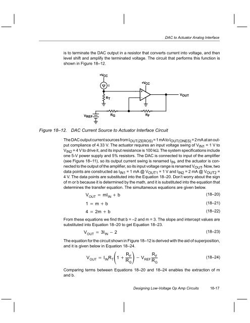
- Page 374 and 375: DAC to Actuator Analog Interface 18
- Page 376 and 377: Comparison of Op Amps 18-20 When DA
- Page 378 and 379: Summary 18.11 Summary 18-22 Always
- Page 380 and 381: 18-24