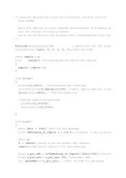
"Chapter 1 - The Op Amp's Place in the World" - HTL Wien 10
"Chapter 1 - The Op Amp's Place in the World" - HTL Wien 10
"Chapter 1 - The Op Amp's Place in the World" - HTL Wien 10

Create successful ePaper yourself
Turn your PDF publications into a flip-book with our unique Google optimized e-Paper software.
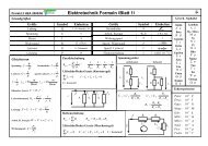
PCB Mechanical Construction<br />
17.2.2.3 Multi-Layer<br />
17-6<br />
Double-sided boards, <strong>in</strong> spite of <strong>the</strong>ir benefits, are not <strong>the</strong> best method of construction,<br />
especially for sensitive or high-speed designs. <strong>The</strong> most common board thickness is<br />
1.5 mm. This separation is too great for full realization of some of <strong>the</strong> benefits listed above.<br />
Distributed capacitance, for example, is very low due to <strong>the</strong> separation.<br />
Critical designs call for multi-layer boards. Some of <strong>the</strong> reasons are obvious:<br />
Better rout<strong>in</strong>g for power as well as ground connections. If <strong>the</strong> power is also on a<br />
plane, it is available to all po<strong>in</strong>ts <strong>in</strong> <strong>the</strong> circuit simply by add<strong>in</strong>g vias.<br />
O<strong>the</strong>r layers are available for signal rout<strong>in</strong>g, mak<strong>in</strong>g rout<strong>in</strong>g easier.<br />
<strong>The</strong>re will be distributed capacitance between <strong>the</strong> power and ground planes,<br />
reduc<strong>in</strong>g high frequency noise.<br />
<strong>The</strong>re are o<strong>the</strong>r reasons for multi-layer boards, however, that may not be obvious or <strong>in</strong>tuitive.<br />
Better EMI/RFI rejection. <strong>The</strong>re is due to <strong>the</strong> image plane effect, which has been<br />
known s<strong>in</strong>ce <strong>the</strong> time of Marconi. When a conductor is placed close to a parallel<br />
conductive surface, most of <strong>the</strong> high frequency currents will return directly under <strong>the</strong><br />
conductor, flow<strong>in</strong>g <strong>in</strong> <strong>the</strong> opposite direction. This mirror image of <strong>the</strong> conductor<br />
with<strong>in</strong> <strong>the</strong> plane creates a transmission l<strong>in</strong>e. S<strong>in</strong>ce currents are equal and opposite<br />
<strong>in</strong> <strong>the</strong> transmission l<strong>in</strong>e, it is relatively immune to radiated noise. It also couples <strong>the</strong><br />
signal very efficiently. <strong>The</strong> image plane effect works equally well with ground and<br />
power planes, but <strong>the</strong>y must be cont<strong>in</strong>uous. Any gap or discont<strong>in</strong>uity causes <strong>the</strong><br />
beneficial effects to quickly vanish. <strong>The</strong>re is more on this <strong>in</strong> <strong>the</strong> follow<strong>in</strong>g<br />
paragraphs.<br />
Reduced overall project cost for small production runs. Although multi-layer boards<br />
are more expensive to manufacture, EMI/RFI requirements from <strong>the</strong> FCC or o<strong>the</strong>r<br />
agencies may require expensive test<strong>in</strong>g of <strong>the</strong> design. If <strong>the</strong>re are problems, it can<br />
force a complete redesign of <strong>the</strong> PCB, lead<strong>in</strong>g to additional rounds of test<strong>in</strong>g. A<br />
multi-layer PCB can have as much as 20-dB better EMI/RFI performance over a<br />
2-layer PCB. If production volumes are go<strong>in</strong>g to be small, it makes sense to make<br />
a better PCB to beg<strong>in</strong> with, than try to cut costs and take <strong>the</strong> risk of fail<strong>in</strong>g $25,000<br />
to $50,000 tests.<br />
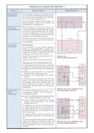
17.2.3 Board Stack-Up — <strong>The</strong> Order of Layers<br />
<strong>The</strong>re has been a lot of confusion <strong>in</strong> <strong>the</strong> past over what is <strong>the</strong> optimum order for PCB<br />
layers. Take, for example, a 4-layer board consist<strong>in</strong>g of two signal layers, a power plane,<br />
and a ground plane. Is it better to route <strong>the</strong> signal traces between <strong>the</strong> layers, thus provid<strong>in</strong>g<br />
shield<strong>in</strong>g for <strong>the</strong> signal traces – or is it better to make <strong>the</strong> ground and power planes<br />
<strong>the</strong> two <strong>in</strong>ner planes?<br />
In consider<strong>in</strong>g this question, it is important to remember that no matter what is decided,<br />
<strong>the</strong>re will still be signals exposed on one or both of <strong>the</strong> top and bottom planes. <strong>The</strong> leads<br />
of <strong>the</strong> op amp PCB package, and <strong>the</strong> traces on <strong>the</strong> board lead<strong>in</strong>g to nearby passive com-