"Chapter 1 - The Op Amp's Place in the World" - HTL Wien 10
"Chapter 1 - The Op Amp's Place in the World" - HTL Wien 10
"Chapter 1 - The Op Amp's Place in the World" - HTL Wien 10

Create successful ePaper yourself
Turn your PDF publications into a flip-book with our unique Google optimized e-Paper software.
<strong>Op</strong>erational Amplifier Parameter Glossary<br />
11-4<br />
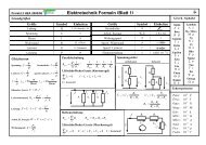
PARAMETER ABBV UNITS DEFINITION INFO<br />
Input capacitance ci pF<br />
Input offset current IIO µA<br />
Input offset voltage<br />
Input offset voltage longterm<br />
drift<br />
VIO,<br />
VOS<br />
mV<br />
V<br />
month<br />
Input resistance ri MΩ<br />
Input voltage range VI V<br />
Large-signal voltage amplification<br />
Lead temperature for <strong>10</strong> or<br />
60 seconds<br />
<strong>The</strong> capacitance between <strong>the</strong> <strong>in</strong>put term<strong>in</strong>als with ei<strong>the</strong>r <strong>in</strong>put<br />
grounded.<br />
<strong>The</strong> difference between <strong>the</strong> currents <strong>in</strong>to <strong>the</strong> two <strong>in</strong>put term<strong>in</strong>als<br />
with <strong>the</strong> output at <strong>the</strong> specified level.<br />
<strong>The</strong> dc voltage that must be applied between <strong>the</strong> <strong>in</strong>put term<strong>in</strong>als<br />
to cancel dc offsets with<strong>in</strong> <strong>the</strong> op amp.<br />
<strong>The</strong> ratio of <strong>the</strong> change <strong>in</strong> <strong>in</strong>put offset voltage to <strong>the</strong> change<br />
time. It is <strong>the</strong> average value for <strong>the</strong> month.<br />
<strong>The</strong> dc resistance between <strong>the</strong> <strong>in</strong>put term<strong>in</strong>als with ei<strong>the</strong>r<br />
<strong>in</strong>put grounded.<br />
<strong>The</strong> range of <strong>in</strong>put voltages that may be applied to ei<strong>the</strong>r <strong>the</strong><br />
IN+ or IN– <strong>in</strong>puts<br />
AV dB (see open loop voltage ga<strong>in</strong>)<br />
°C<br />
Low-level output current IOL mA<br />
Low-level output voltage VOL V<br />
Maximum peak output voltage<br />
sw<strong>in</strong>g<br />
Maximum peak-to-peak output<br />
voltage sw<strong>in</strong>g<br />
Maximum-output-sw<strong>in</strong>g<br />
bandwidth<br />
VOM±<br />
VO(PP)<br />
BOM<br />
V<br />
V<br />
MHz<br />
Noise figure NF dB<br />
<strong>Op</strong>en-loop transimpedance Zt MΩ<br />
<strong>Op</strong>en-loop transresistance Rt MΩ<br />
<strong>Op</strong>en -loop voltage ga<strong>in</strong> AOL dB<br />
<strong>Op</strong>erat<strong>in</strong>g temperature TA °C<br />
Usually specified as an absolute maximum. It is meant to be<br />
used as guide for automated and hand solder<strong>in</strong>g processes.<br />
<strong>The</strong> current <strong>in</strong>to an output with <strong>in</strong>put conditions applied that<br />
accord<strong>in</strong>g to <strong>the</strong> product parameter will establish a low level<br />
at <strong>the</strong> output.<br />
<strong>The</strong> smallest positive op amp output voltage for <strong>the</strong> bias conditions<br />
applied to <strong>the</strong> power p<strong>in</strong>s.<br />
<strong>The</strong> maximum peak-to-peak output voltage that can be obta<strong>in</strong>ed<br />
without clipp<strong>in</strong>g when <strong>the</strong> op amp is operated from a<br />
bipolar supply.<br />
<strong>The</strong> maximum peak-to-peak voltage that can be obta<strong>in</strong>ed<br />
without waveform clipp<strong>in</strong>g when <strong>the</strong> dc output voltage is zero.<br />
<strong>The</strong> range of frequencies with<strong>in</strong> which <strong>the</strong> maximum output<br />
voltage sw<strong>in</strong>g is above a specified value or <strong>the</strong> maximum<br />
frequency of an amplifier <strong>in</strong> which <strong>the</strong> output amplitude is at<br />
<strong>the</strong> extents of it’s l<strong>in</strong>ear range. Also called full power bandwidth.<br />
<strong>The</strong> ratio of <strong>the</strong> total noise power at <strong>the</strong> output of an amplifier,<br />
referred to <strong>the</strong> <strong>in</strong>put, to <strong>the</strong> noise power of <strong>the</strong> signal source.<br />
In a transimpedance or current feedback amplifier, it is <strong>the</strong><br />
frequency dependent ratio of change <strong>in</strong> output voltage to <strong>the</strong><br />
frequency dependent change <strong>in</strong> current at <strong>the</strong> <strong>in</strong>vert<strong>in</strong>g <strong>in</strong>put.<br />
In a transimpedance or current feedback amplifier, it is <strong>the</strong><br />
ratio of change <strong>in</strong> dc output voltage to <strong>the</strong> change <strong>in</strong> dc current<br />
at <strong>the</strong> <strong>in</strong>vert<strong>in</strong>g <strong>in</strong>put.<br />
<strong>The</strong> ratio of change <strong>in</strong> output voltage to <strong>the</strong> change <strong>in</strong> voltage<br />
across <strong>the</strong> <strong>in</strong>put term<strong>in</strong>als. Usually <strong>the</strong> dc value and a graph<br />
show<strong>in</strong>g <strong>the</strong> frequency dependence are shown <strong>in</strong> <strong>the</strong> data<br />
sheet.<br />
Temperature over which <strong>the</strong> op amp may be operated. Some<br />
of <strong>the</strong> o<strong>the</strong>r parameters may change with temperature, lead<strong>in</strong>g<br />
to degraded operation at temperature extremes.<br />
11.3.7.1<br />
11.3.2<br />
11.3.1<br />
11.3.1<br />
11.3.7.1<br />
11.3.15<br />
11.3.5<br />
11.3.5<br />
11.3.15