"Chapter 1 - The Op Amp's Place in the World" - HTL Wien 10
"Chapter 1 - The Op Amp's Place in the World" - HTL Wien 10
"Chapter 1 - The Op Amp's Place in the World" - HTL Wien 10

You also want an ePaper? Increase the reach of your titles
YUMPU automatically turns print PDFs into web optimized ePapers that Google loves.
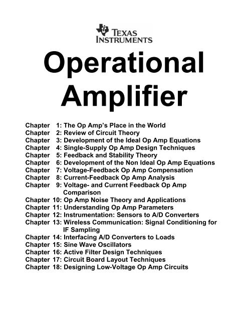
<strong>Op</strong>erational<br />
Amplifier<br />
<strong>Chapter</strong> 1: <strong>The</strong> <strong>Op</strong> Amp’s <strong>Place</strong> <strong>in</strong> <strong>the</strong> World<br />
<strong>Chapter</strong> 2: Review of Circuit <strong>The</strong>ory<br />
<strong>Chapter</strong> 3: Development of <strong>the</strong> Ideal <strong>Op</strong> Amp Equations<br />
<strong>Chapter</strong> 4: S<strong>in</strong>gle-Supply <strong>Op</strong> Amp Design Techniques<br />
<strong>Chapter</strong> 5: Feedback and Stability <strong>The</strong>ory<br />
<strong>Chapter</strong> 6: Development of <strong>the</strong> Non Ideal <strong>Op</strong> Amp Equations<br />
<strong>Chapter</strong> 7: Voltage-Feedback <strong>Op</strong> Amp Compensation<br />
<strong>Chapter</strong> 8: Current-Feedback <strong>Op</strong> Amp Analysis<br />
<strong>Chapter</strong> 9: Voltage- and Current Feedback <strong>Op</strong> Amp<br />
Comparison<br />
<strong>Chapter</strong> <strong>10</strong>: <strong>Op</strong> Amp Noise <strong>The</strong>ory and Applications<br />
<strong>Chapter</strong> 11: Understand<strong>in</strong>g <strong>Op</strong> Amp Parameters<br />
<strong>Chapter</strong> 12: Instrumentation: Sensors to A/D Converters<br />
<strong>Chapter</strong> 13: Wireless Communication: Signal Condition<strong>in</strong>g for<br />
IF Sampl<strong>in</strong>g<br />
<strong>Chapter</strong> 14: Interfac<strong>in</strong>g A/D Converters to Loads<br />
<strong>Chapter</strong> 15: S<strong>in</strong>e Wave Oscillators<br />
<strong>Chapter</strong> 16: Active Filter Design Techniques<br />
<strong>Chapter</strong> 17: Circuit Board Layout Techniques<br />
<strong>Chapter</strong> 18: Design<strong>in</strong>g Low-Voltage <strong>Op</strong> Amp Circuits
<strong>The</strong> <strong>Op</strong> Amp’s <strong>Place</strong> In <strong>The</strong> World<br />
Ron Manc<strong>in</strong>i<br />
<strong>Chapter</strong> 1<br />
In 1934 Harry Black[1] commuted from his home <strong>in</strong> New York City to work at Bell Labs<br />
<strong>in</strong> New Jersey by way of a railroad/ferry. <strong>The</strong> ferry ride relaxed Harry enabl<strong>in</strong>g him to do<br />
some conceptual th<strong>in</strong>k<strong>in</strong>g. Harry had a tough problem to solve; when phone l<strong>in</strong>es were<br />
extended long distances, <strong>the</strong>y needed amplifiers, and undependable amplifiers limited<br />
phone service. First, <strong>in</strong>itial tolerances on <strong>the</strong> ga<strong>in</strong> were poor, but that problem was quickly<br />
solved with an adjustment. Second, even when an amplifier was adjusted correctly at <strong>the</strong><br />
factory, <strong>the</strong> ga<strong>in</strong> drifted so much dur<strong>in</strong>g field operation that <strong>the</strong> volume was too low or <strong>the</strong><br />
<strong>in</strong>com<strong>in</strong>g speech was distorted.<br />
Many attempts had been made to make a stable amplifier, but temperature changes and<br />
power supply voltage extremes experienced on phone l<strong>in</strong>es caused uncontrollable ga<strong>in</strong><br />
drift. Passive components had much better drift characteristics than active components<br />
had, thus if an amplifier’s ga<strong>in</strong> could be made dependent on passive components, <strong>the</strong><br />
problem would be solved. Dur<strong>in</strong>g one of his ferry trips, Harry’s fertile bra<strong>in</strong> conceived a<br />
novel solution for <strong>the</strong> amplifier problem, and he documented <strong>the</strong> solution while rid<strong>in</strong>g on<br />
<strong>the</strong> ferry.<br />
<strong>The</strong> solution was to first build an amplifier that had more ga<strong>in</strong> than <strong>the</strong> application required.<br />
<strong>The</strong>n some of <strong>the</strong> amplifier output signal was fed back to <strong>the</strong> <strong>in</strong>put <strong>in</strong> a manner<br />
that makes <strong>the</strong> circuit ga<strong>in</strong> (circuit is <strong>the</strong> amplifier and feedback components) dependent<br />
on <strong>the</strong> feedback circuit ra<strong>the</strong>r than <strong>the</strong> amplifier ga<strong>in</strong>. Now <strong>the</strong> circuit ga<strong>in</strong> is<br />
dependent on <strong>the</strong> passive feedback components ra<strong>the</strong>r than <strong>the</strong> active amplifier. This is<br />
called negative feedback, and it is <strong>the</strong> underly<strong>in</strong>g operat<strong>in</strong>g pr<strong>in</strong>ciple for all modern day<br />
op amps. Harry had documented <strong>the</strong> first <strong>in</strong>tentional feedback circuit dur<strong>in</strong>g a ferry ride.<br />
I am sure un<strong>in</strong>tentional feedback circuits had been built prior to that time, but <strong>the</strong> designers<br />
ignored <strong>the</strong> effect!<br />
I can hear <strong>the</strong> squeals of anguish com<strong>in</strong>g from <strong>the</strong> managers and amplifier designers. I<br />
imag<strong>in</strong>e that <strong>the</strong>y said someth<strong>in</strong>g like this, “it is hard enough to achieve 30-kHz ga<strong>in</strong>–<br />
bandwidth (GBW), and now this fool wants me to design an amplifier with 3-MHz GBW.<br />
But, he is still go<strong>in</strong>g to get a circuit ga<strong>in</strong> GBW of 30 kHz”. Well, time has proven Harry right,<br />
but <strong>the</strong>re is a m<strong>in</strong>or problem that Harry didn’t discuss <strong>in</strong> detail, and that is <strong>the</strong> oscillation<br />
1-1
1-2<br />
problem. It seems that circuits designed with large open loop ga<strong>in</strong>s sometimes oscillate<br />
when <strong>the</strong> loop is closed. A lot of people <strong>in</strong>vestigated <strong>the</strong> <strong>in</strong>stability effect, and it was pretty<br />
well understood <strong>in</strong> <strong>the</strong> 1940s, but solv<strong>in</strong>g stability problems <strong>in</strong>volved long, tedious, and<br />
<strong>in</strong>tricate calculations. Years passed without anybody mak<strong>in</strong>g <strong>the</strong> problem solution simpler<br />
or more understandable.<br />
In 1945 H. W. Bode presented a system for analyz<strong>in</strong>g <strong>the</strong> stability of feedback systems<br />
by us<strong>in</strong>g graphical methods. Until this time, feedback analysis was done by multiplication<br />
and division, so calculation of transfer functions was a time consum<strong>in</strong>g and laborious task.<br />
Remember, eng<strong>in</strong>eers did not have calculators or computers until <strong>the</strong> ’70s. Bode presented<br />
a log technique that transformed <strong>the</strong> <strong>in</strong>tensely ma<strong>the</strong>matical process of calculat<strong>in</strong>g a<br />
feedback system’s stability <strong>in</strong>to graphical analysis that was simple and perceptive. Feedback<br />
system design was still complicated, but it no longer was an art dom<strong>in</strong>ated by a few<br />
electrical eng<strong>in</strong>eers kept <strong>in</strong> a small dark room. Any electrical eng<strong>in</strong>eer could use Bode’s<br />
methods to f<strong>in</strong>d <strong>the</strong> stability of a feedback circuit, so <strong>the</strong> application of feedback to mach<strong>in</strong>es<br />
began to grow. <strong>The</strong>re really wasn’t much call for electronic feedback design until<br />
computers and transducers become of age.<br />
<strong>The</strong> first real-time computer was <strong>the</strong> analog computer! This computer used preprogrammed<br />
equations and <strong>in</strong>put data to calculate control actions. <strong>The</strong> programm<strong>in</strong>g was<br />
hard wired with a series of circuits that performed math operations on <strong>the</strong> data, and <strong>the</strong><br />
hard wir<strong>in</strong>g limitation eventually caused <strong>the</strong> decl<strong>in</strong><strong>in</strong>g popularity of <strong>the</strong> analog computer.<br />
<strong>The</strong> heart of <strong>the</strong> analog computer was a device called an operational amplifier because<br />
it could be configured to perform many ma<strong>the</strong>matical operations such as multiplication,<br />
addition, subtraction, division, <strong>in</strong>tegration, and differentiation on <strong>the</strong> <strong>in</strong>put signals. <strong>The</strong><br />
name was shortened to <strong>the</strong> familiar op amp, as we have come to know and love <strong>the</strong>m.<br />
<strong>The</strong> op amp used an amplifier with a large open loop ga<strong>in</strong>, and when <strong>the</strong> loop was closed,<br />
<strong>the</strong> amplifier performed <strong>the</strong> ma<strong>the</strong>matical operations dictated by <strong>the</strong> external passive<br />
components. This amplifier was very large because it was built with vacuum tubes and<br />
it required a high-voltage power supply, but it was <strong>the</strong> heart of <strong>the</strong> analog computer, thus<br />
its large size and huge power requirements were accepted as <strong>the</strong> price of do<strong>in</strong>g bus<strong>in</strong>ess.<br />
Many early op amps were designed for analog computers, and it was soon found out that<br />
op amps had o<strong>the</strong>r uses and were very handy to have around <strong>the</strong> physics lab.<br />
At this time general-purpose analog computers were found <strong>in</strong> universities and large company<br />
laboratories because <strong>the</strong>y were critical to <strong>the</strong> research work done <strong>the</strong>re. <strong>The</strong>re was<br />
a parallel requirement for transducer signal condition<strong>in</strong>g <strong>in</strong> lab experiments, and op amps<br />
found <strong>the</strong>ir way <strong>in</strong>to signal condition<strong>in</strong>g applications. As <strong>the</strong> signal condition<strong>in</strong>g applications<br />
expanded, <strong>the</strong> demand for op amps grew beyond <strong>the</strong> analog computer requirements,<br />
and even when <strong>the</strong> analog computers lost favor to digital computers, <strong>the</strong> op amp<br />
survived because of its importance <strong>in</strong> universal analog applications. Eventually digital<br />
computers replaced <strong>the</strong> analog computers (a sad day for real-time measurements), but<br />
<strong>the</strong> demand for op amps <strong>in</strong>creased as measurement applications <strong>in</strong>creased.
<strong>The</strong> first signal condition<strong>in</strong>g op amps were constructed with vacuum tubes prior to <strong>the</strong><br />
<strong>in</strong>troduction of transistors, so <strong>the</strong>y were large and bulky. Dur<strong>in</strong>g <strong>the</strong> ’50s, m<strong>in</strong>iature vacuum<br />
tubes that worked from lower voltage power supplies enabled <strong>the</strong> manufacture of op<br />
amps that shrunk to <strong>the</strong> size of a brick used <strong>in</strong> house construction, so <strong>the</strong> op amp modules<br />
were nicknamed bricks. Vacuum tube size and component size decreased until an op<br />
amp was shrunk to <strong>the</strong> size of a s<strong>in</strong>gle octal vacuum tube. Transistors were commercially<br />
developed <strong>in</strong> <strong>the</strong> ’60s, and <strong>the</strong>y fur<strong>the</strong>r reduced op amp size to several cubic <strong>in</strong>ches, but<br />
<strong>the</strong> nickname brick still held on. Now <strong>the</strong> nickname brick is attached to any electronic module<br />
that uses pott<strong>in</strong>g compound or non-<strong>in</strong>tegrated circuit (IC) packag<strong>in</strong>g methods. Most<br />
of <strong>the</strong>se early op amps were made for specific applications, so <strong>the</strong>y were not necessarily<br />
general purpose. <strong>The</strong> early op amps served a specific purpose, but each manufacturer<br />
had different specifications and packages; hence, <strong>the</strong>re was little second sourc<strong>in</strong>g among<br />
<strong>the</strong> early op amps.<br />
ICs were developed dur<strong>in</strong>g <strong>the</strong> late 1950s and early 1960s, but it wasn’t till <strong>the</strong> middle<br />
1960s that Fairchild released <strong>the</strong> µA709. This was <strong>the</strong> first commercially successful IC<br />
op amp, and Robert J. Widler designed it. <strong>The</strong> µA709 had its share of problems, but any<br />
competent analog eng<strong>in</strong>eer could use it, and it served <strong>in</strong> many different analog applications.<br />
<strong>The</strong> major drawback of <strong>the</strong> µA709 was stability; it required external compensation<br />
and a competent analog eng<strong>in</strong>eer to apply it. Also, <strong>the</strong> µA709 was quite sensitive because<br />
it had a habit of self destruct<strong>in</strong>g under any adverse condition. <strong>The</strong> self-destruction habit<br />
was so prevalent that one major military equipment manufacturer published a paper titled<br />
someth<strong>in</strong>g like, <strong>The</strong> 12 Pearl Harbor Conditions of <strong>the</strong> µA709. <strong>The</strong> µA741 followed <strong>the</strong><br />
µA709, and it is an <strong>in</strong>ternally compensated op amp that does not require external compensation<br />
if operated under data sheet conditions. Also, it is much more forgiv<strong>in</strong>g than<br />
<strong>the</strong> µA709. <strong>The</strong>re has been a never-end<strong>in</strong>g series of new op amps released each year<br />
s<strong>in</strong>ce <strong>the</strong>n, and <strong>the</strong>ir performance and reliability has improved to <strong>the</strong> po<strong>in</strong>t where present<br />
day op amps can be used for analog applications by anybody.<br />
<strong>The</strong> IC op amp is here to stay; <strong>the</strong> latest generation op amps cover <strong>the</strong> frequency spectrum<br />
from 5-kHz GBW to beyond 1-GHz GBW. <strong>The</strong> supply voltage ranges from guaranteed<br />
operation at 0.9 V to absolute maximum voltage rat<strong>in</strong>gs of <strong>10</strong>00 V. <strong>The</strong> <strong>in</strong>put current<br />
and <strong>in</strong>put offset voltage has fallen so low that customers have problems verify<strong>in</strong>g <strong>the</strong><br />
specifications dur<strong>in</strong>g <strong>in</strong>com<strong>in</strong>g <strong>in</strong>spection. <strong>The</strong> op amp has truly become <strong>the</strong> universal<br />
analog IC because it performs all analog tasks. It can function as a l<strong>in</strong>e driver, comparator<br />
(one bit A/D), amplifier, level shifter, oscillator, filter, signal conditioner, actuator driver, current<br />
source, voltage source, and many o<strong>the</strong>r applications. <strong>The</strong> designer’s problem is how<br />
to rapidly select <strong>the</strong> correct circuit/op amp comb<strong>in</strong>ation and <strong>the</strong>n, how to calculate <strong>the</strong> passive<br />
component values that yield <strong>the</strong> desired transfer function <strong>in</strong> <strong>the</strong> circuit.<br />
This book deals with op amp circuits — not with <strong>the</strong> <strong>in</strong>nards of op amps. It treats <strong>the</strong> calculations<br />
from <strong>the</strong> circuit level, and it doesn’t get bogged down <strong>in</strong> a myriad of detailed calculations.<br />
Ra<strong>the</strong>r, <strong>the</strong> reader can start at <strong>the</strong> level appropriate for <strong>the</strong>m, and quickly move<br />
on to <strong>the</strong> advanced topics. If you are look<strong>in</strong>g for material about <strong>the</strong> <strong>in</strong>nards of op amps<br />
1-3
1-4<br />
you are look<strong>in</strong>g <strong>in</strong> <strong>the</strong> wrong place. <strong>The</strong> op amp is treated as a completed component <strong>in</strong><br />
this book.<br />
<strong>The</strong> op amp will cont<strong>in</strong>ue to be a vital component of analog design because it is such a<br />
fundamental component. Each generation of electronics equipment <strong>in</strong>tegrates more<br />
functions on silicon and takes more of <strong>the</strong> analog circuitry <strong>in</strong>side <strong>the</strong> IC. Don’t fear, as digital<br />
applications <strong>in</strong>crease, analog applications also <strong>in</strong>crease because <strong>the</strong> predom<strong>in</strong>ant<br />
supply of data and <strong>in</strong>terface applications are <strong>in</strong> <strong>the</strong> real world, and <strong>the</strong> real world is an analog<br />
world. Thus, each new generation of electronics equipment creates requirements for<br />
new analog circuits; hence, new generations of op amps are required to fulfill <strong>the</strong>se requirements.<br />
Analog design, and op amp design, is a fundamental skill that will be required<br />
far <strong>in</strong>to <strong>the</strong> future.<br />
References<br />
1 Black, H. S., Stabilized Feedback Amplifiers, BSTJ, Vol. 13, January 1934
2.1 Introduction<br />
Review of Circuit <strong>The</strong>ory<br />
Ron Manc<strong>in</strong>i<br />
Although this book m<strong>in</strong>imizes math, some algebra is germane to <strong>the</strong> understand<strong>in</strong>g of<br />
analog electronics. Math and physics are presented here <strong>in</strong> <strong>the</strong> manner <strong>in</strong> which <strong>the</strong>y are<br />
used later, so no practice exercises are given. For example, after <strong>the</strong> voltage divider rule<br />
is expla<strong>in</strong>ed, it is used several times <strong>in</strong> <strong>the</strong> development of o<strong>the</strong>r concepts, and this usage<br />
constitutes practice.<br />
Circuits are a mix of passive and active components. <strong>The</strong> components are arranged <strong>in</strong><br />
a manner that enables <strong>the</strong>m to perform some desired function. <strong>The</strong> result<strong>in</strong>g arrangement<br />
of components is called a circuit or sometimes a circuit configuration. <strong>The</strong> art portion of<br />
analog design is develop<strong>in</strong>g <strong>the</strong> circuit configuration. <strong>The</strong>re are many published circuit<br />
configurations for almost any circuit task, thus all circuit designers need not be artists.<br />
When <strong>the</strong> design has progressed to <strong>the</strong> po<strong>in</strong>t that a circuit exists, equations must be written<br />
to predict and analyze circuit performance. Textbooks are filled with rigorous methods<br />
for equation writ<strong>in</strong>g, and this review of circuit <strong>the</strong>ory does not supplant those textbooks.<br />
But, a few equations are used so often that <strong>the</strong>y should be memorized, and <strong>the</strong>se equations<br />
are considered here.<br />
<strong>The</strong>re are almost as many ways to analyze a circuit as <strong>the</strong>re are electronic eng<strong>in</strong>eers, and<br />
if <strong>the</strong> equations are written correctly, all methods yield <strong>the</strong> same answer. <strong>The</strong>re are some<br />
simple ways to analyze <strong>the</strong> circuit without complet<strong>in</strong>g unnecessary calculations, and<br />
<strong>the</strong>se methods are illustrated here.<br />
2.2 Laws of Physics<br />
<strong>Chapter</strong> 2<br />
Ohm’s law is stated as V=IR, and it is fundamental to all electronics. Ohm’s law can be<br />
applied to a s<strong>in</strong>gle component, to any group of components, or to a complete circuit. When<br />
<strong>the</strong> current flow<strong>in</strong>g through any portion of a circuit is known, <strong>the</strong> voltage dropped across<br />
that portion of <strong>the</strong> circuit is obta<strong>in</strong>ed by multiply<strong>in</strong>g <strong>the</strong> current times <strong>the</strong> resistance (Equation<br />
2–1).<br />
2-1
Laws of Physics<br />
2-2<br />
V IR<br />
(2–1)<br />
In Figure 2–1, Ohm’s law is applied to <strong>the</strong> total circuit. <strong>The</strong> current, (I) flows through <strong>the</strong><br />
total resistance (R), and <strong>the</strong> voltage (V) is dropped across R.<br />
I<br />
V R<br />
Figure 2–1. Ohm’s Law Applied to <strong>the</strong> Total Circuit<br />
In Figure 2–2, Ohm’s law is applied to a s<strong>in</strong>gle component. <strong>The</strong> current (I R) flows through<br />
<strong>the</strong> resistor (R) and <strong>the</strong> voltage (V R) is dropped across R. Notice, <strong>the</strong> same formula is used<br />
to calculate <strong>the</strong> voltage drop across R even though it is only a part of <strong>the</strong> circuit.<br />
IR<br />
V R<br />
Figure 2–2. Ohm’s Law Applied to a Component<br />
Kirchoff’s voltage law states that <strong>the</strong> sum of <strong>the</strong> voltage drops <strong>in</strong> a series circuit equals<br />
<strong>the</strong> sum of <strong>the</strong> voltage sources. O<strong>the</strong>rwise, <strong>the</strong> source (or sources) voltage must be<br />
dropped across <strong>the</strong> passive components. When tak<strong>in</strong>g sums keep <strong>in</strong> m<strong>in</strong>d that <strong>the</strong> sum<br />
is an algebraic quantity. Kirchoff’s voltage law is illustrated <strong>in</strong> Figure 2–3 and Equations<br />
2–2 and 2–3.<br />
Figure 2–3. Kirchoff’s Voltage Law<br />
R1<br />
VR1<br />
V R2<br />
V SOURCES V DROPS<br />
V V R1 V R2<br />
VR<br />
VR2<br />
(2–2)<br />
(2–3)<br />
Kirchoff’s current law states: <strong>the</strong> sum of <strong>the</strong> currents enter<strong>in</strong>g a junction equals <strong>the</strong> sum<br />
of <strong>the</strong> currents leav<strong>in</strong>g a junction. It makes no difference if a current flows from a current
Voltage Divider Rule<br />
source, through a component, or through a wire, because all currents are treated identically.<br />
Kirchoff’s current law is illustrated <strong>in</strong> Figure 2–4 and Equations 2–4 and 2–5.<br />
Figure 2–4. Kirchoff’s Current Law<br />
2.3 Voltage Divider Rule<br />
I1<br />
I IN I OUT<br />
I 1 I 2 I 3 I 4<br />
I4 I3<br />
I2<br />
Review of Circuit <strong>The</strong>ory<br />
(2–4)<br />
(2–5)<br />
When <strong>the</strong> output of a circuit is not loaded, <strong>the</strong> voltage divider rule can be used to calculate<br />
<strong>the</strong> circuit’s output voltage. Assume that <strong>the</strong> same current flows through all circuit elements<br />
(Figure 2–5). Equation 2–6 is written us<strong>in</strong>g Ohm’s law as V = I (R 1 + R 2). Equation<br />
2–7 is written as Ohm’s law across <strong>the</strong> output resistor.<br />
Figure 2–5. Voltage Divider Rule<br />
I <br />
V R2<br />
V<br />
R 1 R 2<br />
V OUT IR 2<br />
I<br />
R1<br />
I<br />
VO<br />
(2–6)<br />
(2–7)<br />
Substitut<strong>in</strong>g Equation 2–6 <strong>in</strong>to Equation 2–7, and us<strong>in</strong>g algebraic manipulation yields<br />
Equation 2–8.<br />
V OUT V<br />
R 2<br />
R 1 R 2<br />
(2–8)<br />
A simple way to remember <strong>the</strong> voltage divider rule is that <strong>the</strong> output resistor is divided by<br />
<strong>the</strong> total circuit resistance. This fraction is multiplied by <strong>the</strong> <strong>in</strong>put voltage to obta<strong>in</strong> <strong>the</strong> out-<br />
2-3
Current Divider Rule<br />
2-4<br />
put voltage. Remember that <strong>the</strong> voltage divider rule always assumes that <strong>the</strong> output resistor<br />
is not loaded; <strong>the</strong> equation is not valid when <strong>the</strong> output resistor is loaded by a parallel<br />
component. Fortunately, most circuits follow<strong>in</strong>g a voltage divider are <strong>in</strong>put circuits, and<br />
<strong>in</strong>put circuits are usually high resistance circuits. When a fixed load is <strong>in</strong> parallel with <strong>the</strong><br />
output resistor, <strong>the</strong> equivalent parallel value comprised of <strong>the</strong> output resistor and load<strong>in</strong>g<br />
resistor can be used <strong>in</strong> <strong>the</strong> voltage divider calculations with no error. Many people ignore<br />
<strong>the</strong> load resistor if it is ten times greater than <strong>the</strong> output resistor value, but this calculation<br />
can lead to a <strong>10</strong>% error.<br />
2.4 Current Divider Rule<br />
When <strong>the</strong> output of a circuit is not loaded, <strong>the</strong> current divider rule can be used to calculate<br />
<strong>the</strong> current flow <strong>in</strong> <strong>the</strong> output branch circuit (R 2). <strong>The</strong> currents I 1 and I 2 <strong>in</strong> Figure 2–6 are<br />
assumed to be flow<strong>in</strong>g <strong>in</strong> <strong>the</strong> branch circuits. Equation 2–9 is written with <strong>the</strong> aid of Kirchoff’s<br />
current law. <strong>The</strong> circuit voltage is written <strong>in</strong> Equation 2–<strong>10</strong> with <strong>the</strong> aid of Ohm’s law.<br />
Comb<strong>in</strong><strong>in</strong>g Equations 2–9 and 2–<strong>10</strong> yields Equation 2–11.<br />
Figure 2–6. Current Divider Rule<br />
I I 1 I 2<br />
I1 I2<br />
I R1 R2<br />
V I 1 R 1 I 2 R 2<br />
I I 1 I 2 I 2<br />
R2 R1 V<br />
I2 I2R1 R2 R1 Rearrang<strong>in</strong>g <strong>the</strong> terms <strong>in</strong> Equation 2–11 yields Equation 2–12.<br />
I2 I R1 R1 R2 (2–9)<br />
(2–<strong>10</strong>)<br />
(2–11)<br />
(2–12)<br />
<strong>The</strong> total circuit current divides <strong>in</strong>to two parts, and <strong>the</strong> resistance (R 1) divided by <strong>the</strong> total<br />
resistance determ<strong>in</strong>es how much current flows through R 2. An easy method of remember<strong>in</strong>g<br />
<strong>the</strong> current divider rule is to remember <strong>the</strong> voltage divider rule. <strong>The</strong>n modify <strong>the</strong> voltage<br />
divider rule such that <strong>the</strong> opposite resistor is divided by <strong>the</strong> total resistance, and <strong>the</strong> fraction<br />
is multiplied by <strong>the</strong> <strong>in</strong>put current to get <strong>the</strong> branch current.
2.5 <strong>The</strong>ven<strong>in</strong>’s <strong>The</strong>orem<br />
Review of Circuit <strong>The</strong>ory<br />
<strong>The</strong>ven<strong>in</strong>’s <strong>The</strong>orem<br />
<strong>The</strong>re are times when it is advantageous to isolate a part of <strong>the</strong> circuit to simplify <strong>the</strong> analysis<br />
of <strong>the</strong> isolated part of <strong>the</strong> circuit. Ra<strong>the</strong>r than write loop or node equations for <strong>the</strong> complete<br />
circuit, and solv<strong>in</strong>g <strong>the</strong>m simultaneously, <strong>The</strong>ven<strong>in</strong>’s <strong>the</strong>orem enables us to isolate<br />
<strong>the</strong> part of <strong>the</strong> circuit we are <strong>in</strong>terested <strong>in</strong>. We <strong>the</strong>n replace <strong>the</strong> rema<strong>in</strong><strong>in</strong>g circuit with a<br />
simple series equivalent circuit, thus <strong>The</strong>ven<strong>in</strong>’s <strong>the</strong>orem simplifies <strong>the</strong> analysis.<br />
<strong>The</strong>re are two <strong>the</strong>orems that do similar functions. <strong>The</strong> <strong>The</strong>ven<strong>in</strong> <strong>the</strong>orem just described<br />
is <strong>the</strong> first, and <strong>the</strong> second is called Norton’s <strong>the</strong>orem. <strong>The</strong>ven<strong>in</strong>’s <strong>the</strong>orem is used when<br />
<strong>the</strong> <strong>in</strong>put source is a voltage source, and Norton’s <strong>the</strong>orem is used when <strong>the</strong> <strong>in</strong>put source<br />
is a current source. Norton’s <strong>the</strong>orem is rarely used, so its explanation is left for <strong>the</strong> reader<br />
to dig out of a textbook if it is ever required.<br />
<strong>The</strong> rules for <strong>The</strong>ven<strong>in</strong>’s <strong>the</strong>orem start with <strong>the</strong> component or part of <strong>the</strong> circuit be<strong>in</strong>g replaced.<br />
Referr<strong>in</strong>g to Figure 2–7, look back <strong>in</strong>to <strong>the</strong> term<strong>in</strong>als (left from C and R 3 toward<br />
po<strong>in</strong>t XX <strong>in</strong> <strong>the</strong> figure) of <strong>the</strong> circuit be<strong>in</strong>g replaced. Calculate <strong>the</strong> no load voltage (V TH)<br />
as seen from <strong>the</strong>se term<strong>in</strong>als (use <strong>the</strong> voltage divider rule).<br />
Figure 2–7. Orig<strong>in</strong>al Circuit<br />
V<br />
R1<br />
R2<br />
X<br />
X<br />
Look <strong>in</strong>to <strong>the</strong> term<strong>in</strong>als of <strong>the</strong> circuit be<strong>in</strong>g replaced, short <strong>in</strong>dependent voltage sources,<br />
and calculate <strong>the</strong> impedance between <strong>the</strong>se term<strong>in</strong>als. <strong>The</strong> f<strong>in</strong>al step is to substitute <strong>the</strong><br />
<strong>The</strong>ven<strong>in</strong> equivalent circuit for <strong>the</strong> part you wanted to replace as shown <strong>in</strong> Figure 2–8.<br />
VTH<br />
RTH<br />
Figure 2–8. <strong>The</strong>ven<strong>in</strong>’s Equivalent Circuit for Figure 2–7<br />
X<br />
X<br />
R3<br />
<strong>The</strong> <strong>The</strong>ven<strong>in</strong> equivalent circuit is a simple series circuit, thus fur<strong>the</strong>r calculations are simplified.<br />
<strong>The</strong> simplification of circuit calculations is often sufficient reason to use <strong>The</strong>ven<strong>in</strong>’s<br />
R3<br />
C<br />
C<br />
2-5
<strong>The</strong>ven<strong>in</strong>’s <strong>The</strong>orem<br />
2-6<br />
V<br />
<strong>the</strong>orem because it elim<strong>in</strong>ates <strong>the</strong> need for solv<strong>in</strong>g several simultaneous equations. <strong>The</strong><br />
detailed <strong>in</strong>formation about what happens <strong>in</strong> <strong>the</strong> circuit that was replaced is not available<br />
when us<strong>in</strong>g <strong>The</strong>ven<strong>in</strong>’s <strong>the</strong>orem, but that is no consequence because you had no <strong>in</strong>terest<br />
<strong>in</strong> it.<br />
As an example of <strong>The</strong>ven<strong>in</strong>’s <strong>the</strong>orem, let’s calculate <strong>the</strong> output voltage (V OUT) shown <strong>in</strong><br />
Figure 2–9A. <strong>The</strong> first step is to stand on <strong>the</strong> term<strong>in</strong>als X–Y with your back to <strong>the</strong> output<br />
circuit, and calculate <strong>the</strong> open circuit voltage seen (V TH). This is a perfect opportunity to<br />
use <strong>the</strong> voltage divider rule to obta<strong>in</strong> Equation 2–13.<br />
R1<br />
R2<br />
X<br />
Y<br />
R3<br />
(a) <strong>The</strong> Orig<strong>in</strong>al Circuit<br />
VOUT<br />
Figure 2–9. Example of <strong>The</strong>ven<strong>in</strong>’s Equivalent Circuit<br />
V TH V<br />
R4<br />
R 2<br />
R 1 R 2<br />
VTH<br />
RTH<br />
X<br />
Y<br />
R3<br />
R4<br />
(b) <strong>The</strong> <strong>The</strong>ven<strong>in</strong> Equivalent Circuit<br />
VOUT<br />
(2–13)<br />
Still stand<strong>in</strong>g on <strong>the</strong> term<strong>in</strong>als X-Y, step two is to calculate <strong>the</strong> impedance seen look<strong>in</strong>g<br />
<strong>in</strong>to <strong>the</strong>se term<strong>in</strong>als (short <strong>the</strong> voltage sources). <strong>The</strong> <strong>The</strong>ven<strong>in</strong> impedance is <strong>the</strong> parallel<br />
impedance of R 1 and R 2 as calculated <strong>in</strong> Equation 2–14. Now get off <strong>the</strong> term<strong>in</strong>als X-Y<br />
before you damage <strong>the</strong>m with your big feet. Step three replaces <strong>the</strong> circuit to <strong>the</strong> left of<br />
X-Y with <strong>the</strong> <strong>The</strong>ven<strong>in</strong> equivalent circuit V TH and R TH.<br />
RTH R1R2 R <br />
R1 R 1 R2 2<br />
(2–14)<br />
Note:<br />
Two parallel vertical bars ( || ) are used to <strong>in</strong>dicate parallel components as<br />
shown <strong>in</strong> Equation 2–14.<br />
<strong>The</strong> f<strong>in</strong>al step is to calculate <strong>the</strong> output voltage. Notice <strong>the</strong> voltage divider rule is used<br />
aga<strong>in</strong>. Equation 2–15 describes <strong>the</strong> output voltage, and it comes out naturally <strong>in</strong> <strong>the</strong> form<br />
of a series of voltage dividers, which makes sense. That’s ano<strong>the</strong>r advantage of <strong>the</strong> voltage<br />
divider rule; <strong>the</strong> answers normally come out <strong>in</strong> a recognizable form ra<strong>the</strong>r than a<br />
jumble of coefficients and parameters.
V OUT V TH<br />
R4 V RTH R3 R4 R2 R4 R1 R2 R1R2 R<br />
R 3 R4 1R2 Review of Circuit <strong>The</strong>ory<br />
<strong>The</strong>ven<strong>in</strong>’s <strong>The</strong>orem<br />
(2–15)<br />
<strong>The</strong> circuit analysis is done <strong>the</strong> hard way <strong>in</strong> Figure 2–<strong>10</strong>, so you can see <strong>the</strong> advantage<br />
of us<strong>in</strong>g <strong>The</strong>ven<strong>in</strong>’s <strong>The</strong>orem. Two loop currents, I 1 and I 2, are assigned to <strong>the</strong> circuit.<br />
<strong>The</strong>n <strong>the</strong> loop Equations 2–16 and 2–17 are written.<br />
Figure 2–<strong>10</strong>. Analysis Done <strong>the</strong> Hard Way<br />
V<br />
R1<br />
I1<br />
R2<br />
V I 1 R 1 R 2 I 2 R 2<br />
R3<br />
I 2 R 2 R 3 R 4 I 1 R 2<br />
I2<br />
R4<br />
VOUT<br />
(2–16)<br />
(2–17)<br />
Equation 2–17 is rewritten as Equation 2–18 and substituted <strong>in</strong>to Equation 2–16 to obta<strong>in</strong><br />
Equation 2–19.<br />
I 1 I 2<br />
R 2 R 3 R 4<br />
R 2<br />
V I2 R2 R3 R4R R 1 R 2 I2R2 2<br />
(2–18)<br />
(2–19)<br />
<strong>The</strong> terms are rearranged <strong>in</strong> Equation 2–20. Ohm’s law is used to write Equation 2–21,<br />
and <strong>the</strong> f<strong>in</strong>al substitutions are made <strong>in</strong> Equation 2–22.<br />
I 2 <br />
V<br />
R2R3R 4 R<br />
R 1 R 2 R2 2<br />
V OUT I 2 R 4<br />
V OUT V<br />
R 4<br />
R2R3R R 4 1R 2<br />
R2 R 2<br />
(2–20)<br />
(2–21)<br />
(2–22)<br />
This is a lot of extra work for no ga<strong>in</strong>. Also, <strong>the</strong> answer is not <strong>in</strong> a usable form because<br />
<strong>the</strong> voltage dividers are not recognizable, thus more algebra is required to get <strong>the</strong> answer<br />
<strong>in</strong>to usable form.<br />
2-7
Superposition<br />
2.6 Superposition<br />
2-8<br />
Superposition is a <strong>the</strong>orem that can be applied to any l<strong>in</strong>ear circuit. Essentially, when<br />
<strong>the</strong>re are <strong>in</strong>dependent sources, <strong>the</strong> voltages and currents result<strong>in</strong>g from each source can<br />
be calculated separately, and <strong>the</strong> results are added algebraically. This simplifies <strong>the</strong> calculations<br />
because it elim<strong>in</strong>ates <strong>the</strong> need to write a series of loop or node equations. An<br />
example is shown <strong>in</strong> Figure 2–11.<br />
V1<br />
Figure 2–11.Superposition Example<br />
R1<br />
R3<br />
V2<br />
R2<br />
VOUT<br />
When V 1 is grounded, V 2 forms a voltage divider with R 3 and <strong>the</strong> parallel comb<strong>in</strong>ation of<br />
R 2 and R 1. <strong>The</strong> output voltage for this circuit (V OUT2) is calculated with <strong>the</strong> aid of <strong>the</strong> voltage<br />
divider equation (2–23). <strong>The</strong> circuit is shown <strong>in</strong> Figure 2–12. <strong>The</strong> voltage divider rule<br />
yields <strong>the</strong> answer quickly.<br />
Figure 2–12. When V 1 is Grounded<br />
V OUT2 V 2<br />
R3<br />
V2 R1 R2 VOUT2<br />
R 1 R 2<br />
R 3 R 1 R 2<br />
(2–23)<br />
Likewise, when V 2 is grounded (Figure 2–13), V 1 forms a voltage divider with R 1 and <strong>the</strong><br />
parallel comb<strong>in</strong>ation of R 3 and R 2, and <strong>the</strong> voltage divider <strong>the</strong>orem is applied aga<strong>in</strong> to calculate<br />
V OUT (Equation 2–24).<br />
Figure 2–13. When V 2 is Grounded<br />
R1<br />
V1 R3 R2 VOUT1
V OUT1 V 1<br />
R 2 R 3<br />
R 1 R 2 R 3<br />
Calculation of a Saturated Transistor Circuit<br />
Review of Circuit <strong>The</strong>ory<br />
(2–24)<br />
After <strong>the</strong> calculations for each source are made <strong>the</strong> components are added to obta<strong>in</strong> <strong>the</strong><br />
f<strong>in</strong>al solution (Equation 2–25).<br />
R2 R3 R1 R2 VOUT V1 V2 R1 R2 R3 R3 R1 R2 (2–25)<br />
<strong>The</strong> reader should analyze this circuit with loop or node equations to ga<strong>in</strong> an appreciation<br />
for superposition. Aga<strong>in</strong>, <strong>the</strong> superposition results come out as a simple arrangement that<br />
is easy to understand. One looks at <strong>the</strong> f<strong>in</strong>al equation and it is obvious that if <strong>the</strong> sources<br />
are equal and opposite polarity, and when R 1 = R 3, <strong>the</strong>n <strong>the</strong> output voltage is zero. Conclusions<br />
such as this are hard to make after <strong>the</strong> results of a loop or node analysis unless considerable<br />
effort is made to manipulate <strong>the</strong> f<strong>in</strong>al equation <strong>in</strong>to symmetrical form.<br />
2.7 Calculation of a Saturated Transistor Circuit<br />
<strong>The</strong> circuit specifications are: when V IN = 12 V, V OUT
Transistor Amplifier<br />
2-<strong>10</strong><br />
I C I B V 12 V CE<br />
R C<br />
R B V IN V BE<br />
I B<br />
IL V12 I<br />
R L<br />
C<br />
Substitut<strong>in</strong>g Equation 2–27 <strong>in</strong>to Equation 2–28 yields Equation 2–29.<br />
R B V IN V BE <br />
I C<br />
<br />
(12 0.6)50 V<br />
12 2 (<strong>10</strong>)<br />
35.6 k<br />
mA<br />
(2–27)<br />
(2–28)<br />
(2–29)<br />
When <strong>the</strong> transistor goes on it s<strong>in</strong>ks <strong>the</strong> load current, and it still goes <strong>in</strong>to saturation. <strong>The</strong>se<br />
calculations neglect some m<strong>in</strong>or details, but <strong>the</strong>y are <strong>in</strong> <strong>the</strong> 98% accuracy range.<br />
2.8 Transistor Amplifier<br />
<strong>The</strong> amplifier is an analog circuit (Figure 2–15), and <strong>the</strong> calculations, plus <strong>the</strong> po<strong>in</strong>ts that<br />
must be considered dur<strong>in</strong>g <strong>the</strong> design, are more complicated than for a saturated circuit.<br />
This extra complication leads people to say that analog design is harder than digital design<br />
(<strong>the</strong> saturated transistor is digital i.e.; on or off). Analog design is harder than digital<br />
design because <strong>the</strong> designer must account for all states <strong>in</strong> analog, whereas <strong>in</strong> digital only<br />
two states must be accounted for. <strong>The</strong> specifications for <strong>the</strong> amplifier are an ac voltage<br />
ga<strong>in</strong> of four and a peak-to-peak signal sw<strong>in</strong>g of 4 volts.<br />
VIN<br />
Figure 2–15. Transistor Amplifier<br />
CIN<br />
12 V<br />
R2<br />
R1<br />
RE1<br />
RE2<br />
12 V<br />
RC<br />
CE<br />
VOUT<br />
I C is selected as <strong>10</strong> mA because <strong>the</strong> transistor has a current ga<strong>in</strong> (β) of <strong>10</strong>0 at that po<strong>in</strong>t.<br />
<strong>The</strong> collector voltage is arbitrarily set at 8 V; when <strong>the</strong> collector voltage sw<strong>in</strong>gs positive
Review of Circuit <strong>The</strong>ory<br />
Transistor Amplifier<br />
2 V (from 8 V to <strong>10</strong> V) <strong>the</strong>re is still enough voltage dropped across R C to keep <strong>the</strong> transistor<br />
on. Set <strong>the</strong> collector-emitter voltage at 4 V; when <strong>the</strong> collector voltage sw<strong>in</strong>gs negative<br />
2 V (from 8 V to 6 V) <strong>the</strong> transistor still has 2 V across it, so it stays l<strong>in</strong>ear. This sets <strong>the</strong><br />
emitter voltage (V E) at 4 V.<br />
R C V 12 V C<br />
I C<br />
R E R E1 R E2 V E<br />
I E<br />
<br />
12 V 8V<br />
<strong>10</strong> mA<br />
400 <br />
VE <br />
IB IC VE <br />
IC 4V<br />
400 <br />
<strong>10</strong> mA<br />
Use <strong>The</strong>ven<strong>in</strong>’s equivalent circuit to calculate R 1 and R 2 as shown <strong>in</strong> Figure 2–16.<br />
R2<br />
12<br />
R1 + R2<br />
R1 || R2<br />
Figure 2–16. <strong>The</strong>ven<strong>in</strong> Equivalent of <strong>the</strong> Base Circuit<br />
I B I C<br />
<br />
<strong>10</strong> mA<br />
<strong>10</strong>0<br />
V TH 12R 2<br />
R 1 R 2<br />
R TH R 1 R 2<br />
R 1 R 2<br />
IB<br />
0.1 mA<br />
VB = 4.6 V<br />
(2–30)<br />
(2–31)<br />
(2–32)<br />
(2–33)<br />
(2–34)<br />
We want <strong>the</strong> base voltage to be 4.6 V because <strong>the</strong> emitter voltage is <strong>the</strong>n 4 V. Assume<br />
a voltage drop of 0.4 V across R TH, so Equation 2–35 can be written. <strong>The</strong> drop across R TH<br />
may not be exactly 0.4 V because of beta variations, but a few hundred mV does not matter<br />
is this design. Now, calculate <strong>the</strong> ratio of R 1 and R 2 us<strong>in</strong>g <strong>the</strong> voltage divider rule (<strong>the</strong><br />
load current has been accounted for).<br />
RTH 0.4<br />
k 4k<br />
0.1<br />
VTH IBRTh VB 0.4 4.6 5 12<br />
R1 R2 R 2 7<br />
5 R 1<br />
R 2<br />
(2–35)<br />
(2–36)<br />
(2–37)<br />
R 1 is almost equal to R 2, thus select<strong>in</strong>g R 1 as twice <strong>the</strong> <strong>The</strong>ven<strong>in</strong> resistance yields approximately<br />
4 K as shown <strong>in</strong> Equation 2–35. Hence, R 1 = 11.2 k and R 2 = 8 k. <strong>The</strong> ac ga<strong>in</strong> is<br />
2-11
Transistor Amplifier<br />
2-12<br />
approximately R C/R E1 because C E shorts out R E2 at high frequencies, so we can write<br />
Equation 2–38.<br />
R E1 R C<br />
G<br />
400<br />
4<br />
<strong>10</strong>0 <br />
R E2 R E R E1 400 <strong>10</strong>0 300 <br />
(2–38)<br />
(2–39)<br />
<strong>The</strong> capacitor selection depends on <strong>the</strong> frequency response required for <strong>the</strong> amplifier, but<br />
<strong>10</strong> µF for C IN and <strong>10</strong>00 µF for C E suffice for a start<strong>in</strong>g po<strong>in</strong>t.
Development of <strong>the</strong> Ideal <strong>Op</strong> Amp Equations<br />
3.1 Ideal <strong>Op</strong> Amp Assumptions<br />
Ron Manc<strong>in</strong>i<br />
<strong>Chapter</strong> 3<br />
<strong>The</strong> name Ideal <strong>Op</strong> Amp is applied to this and similar analysis because <strong>the</strong> salient parameters<br />
of <strong>the</strong> op amp are assumed to be perfect. <strong>The</strong>re is no such th<strong>in</strong>g as an ideal op amp,<br />
but present day op amps come so close to ideal that Ideal <strong>Op</strong> Amp analysis approaches<br />
actual analysis. <strong>Op</strong> amps depart from <strong>the</strong> ideal <strong>in</strong> two ways. First, dc parameters such as<br />
<strong>in</strong>put offset voltage are large enough to cause departure from <strong>the</strong> ideal. <strong>The</strong> ideal assumes<br />
that <strong>in</strong>put offset voltage is zero. Second, ac parameters such as ga<strong>in</strong> are a function<br />
of frequency, so <strong>the</strong>y go from large values at dc to small values at high frequencies.<br />
This assumption simplifies <strong>the</strong> analysis, thus it clears <strong>the</strong> path for <strong>in</strong>sight. It is so much<br />
easier to see <strong>the</strong> forest when <strong>the</strong> brush and huge trees are cleared away. Although <strong>the</strong><br />
ideal op amp analysis makes use of perfect parameters, <strong>the</strong> analysis is often valid because<br />
some op amps approach perfection. In addition, when work<strong>in</strong>g at low frequencies,<br />
several kHz, <strong>the</strong> ideal op amp analysis produces accurate answers. Voltage feedback op<br />
amps are covered <strong>in</strong> this chapter, and current feedback op amps are covered <strong>in</strong> <strong>Chapter</strong><br />
8.<br />
Several assumptions have to be made before <strong>the</strong> ideal op amp analysis can proceed.<br />
First, assume that <strong>the</strong> current flow <strong>in</strong>to <strong>the</strong> <strong>in</strong>put leads of <strong>the</strong> op amp is zero. This assumption<br />
is almost true <strong>in</strong> FET op amps where <strong>in</strong>put currents can be less than a pA, but this<br />
is not always true <strong>in</strong> bipolar high-speed op amps where tens of µA <strong>in</strong>put currents are<br />
found.<br />
Second, <strong>the</strong> op amp ga<strong>in</strong> is assumed to be <strong>in</strong>f<strong>in</strong>ite, hence it drives <strong>the</strong> output voltage to<br />
any value to satisfy <strong>the</strong> <strong>in</strong>put conditions. This assumes that <strong>the</strong> op amp output voltage can<br />
achieve any value. In reality, saturation occurs when <strong>the</strong> output voltage comes close to<br />
a power supply rail, but reality does not negate <strong>the</strong> assumption, it only bounds it.<br />
Also, implicit <strong>in</strong> <strong>the</strong> <strong>in</strong>f<strong>in</strong>ite ga<strong>in</strong> assumption is <strong>the</strong> need for zero <strong>in</strong>put signal. <strong>The</strong> ga<strong>in</strong><br />
drives <strong>the</strong> output voltage until <strong>the</strong> voltage between <strong>the</strong> <strong>in</strong>put leads (<strong>the</strong> error voltage) is<br />
zero. This leads to <strong>the</strong> third assumption that <strong>the</strong> voltage between <strong>the</strong> <strong>in</strong>put leads is zero.<br />
<strong>The</strong> implication of zero voltage between <strong>the</strong> <strong>in</strong>put leads means that if one <strong>in</strong>put is tied to<br />
3-1
Ideal <strong>Op</strong> Amp Assumptions<br />
3-2<br />
a hard voltage source such as ground, <strong>the</strong>n <strong>the</strong> o<strong>the</strong>r <strong>in</strong>put is at <strong>the</strong> same potential. <strong>The</strong><br />
current flow <strong>in</strong>to <strong>the</strong> <strong>in</strong>put leads is zero, so <strong>the</strong> <strong>in</strong>put impedance of <strong>the</strong> op amp is <strong>in</strong>f<strong>in</strong>ite.<br />
Fourth, <strong>the</strong> output impedance of <strong>the</strong> ideal op amp is zero. <strong>The</strong> ideal op amp can drive any<br />
load without an output impedance dropp<strong>in</strong>g voltage across it. <strong>The</strong> output impedance of<br />
most op amps is a fraction of an ohm for low current flows, so this assumption is valid <strong>in</strong><br />
most cases. Fifth, <strong>the</strong> frequency response of <strong>the</strong> ideal op amp is flat; this means that <strong>the</strong><br />
ga<strong>in</strong> does not vary as frequency <strong>in</strong>creases. By constra<strong>in</strong><strong>in</strong>g <strong>the</strong> use of <strong>the</strong> op amp to <strong>the</strong><br />
low frequencies, we make <strong>the</strong> frequency response assumption true.<br />
Table 3–1 lists <strong>the</strong> basic ideal op amp assumptions and FIgure 3–1shows <strong>the</strong> ideal op<br />
amp.<br />
Table 3–1. Basic Ideal <strong>Op</strong> Amp Assumptions<br />
IB = 0<br />
VE = 0<br />
IB = 0<br />
Figure 3–1. <strong>The</strong> Ideal <strong>Op</strong> Amp<br />
PARAMETER NAME PARAMETERS SYMBOL VALUE<br />
Input current IIN 0<br />
Input offset voltage VOS 0<br />
Input impedance ZIN ∞<br />
Output impedance ZOUT 0<br />
Ga<strong>in</strong> a ∞<br />
_<br />
+<br />
Zi = ∝<br />
ZO = 0<br />
a = ∝<br />
VOUT
3.2 <strong>The</strong> Non<strong>in</strong>vert<strong>in</strong>g <strong>Op</strong> Amp<br />
<strong>The</strong> Non<strong>in</strong>vert<strong>in</strong>g <strong>Op</strong> Amp<br />
<strong>The</strong> non<strong>in</strong>vert<strong>in</strong>g op amp has <strong>the</strong> <strong>in</strong>put signal connected to its non<strong>in</strong>vert<strong>in</strong>g <strong>in</strong>put (Figure<br />
3–2), thus its <strong>in</strong>put source sees an <strong>in</strong>f<strong>in</strong>ite impedance. <strong>The</strong>re is no <strong>in</strong>put offset voltage because<br />
V OS = V E = 0, hence <strong>the</strong> negative <strong>in</strong>put must be at <strong>the</strong> same voltage as <strong>the</strong> positive<br />
<strong>in</strong>put. <strong>The</strong> op amp output drives current <strong>in</strong>to R F until <strong>the</strong> negative <strong>in</strong>put is at <strong>the</strong> voltage,<br />
V IN. This action causes V IN to appear across R G.<br />
VIN<br />
Figure 3–2. <strong>The</strong> Non<strong>in</strong>vert<strong>in</strong>g <strong>Op</strong> Amp<br />
IB = 0<br />
VE<br />
VIN<br />
+<br />
a<br />
_<br />
RF<br />
RG<br />
VOUT<br />
<strong>The</strong> voltage divider rule is used to calculate V IN; V OUT is <strong>the</strong> <strong>in</strong>put to <strong>the</strong> voltage divider,<br />
and V IN is <strong>the</strong> output of <strong>the</strong> voltage divider. S<strong>in</strong>ce no current can flow <strong>in</strong>to ei<strong>the</strong>r op amp<br />
lead, use of <strong>the</strong> voltage divider rule is allowed. Equation 3–1 is written with <strong>the</strong> aid of <strong>the</strong><br />
voltage divider rule, and algebraic manipulation yields Equation 3–2 <strong>in</strong> <strong>the</strong> form of a ga<strong>in</strong><br />
parameter.<br />
V IN V OUT<br />
V OUT<br />
V IN<br />
R G<br />
R G R F<br />
R G R F<br />
R G<br />
1 R F<br />
R G<br />
Development of <strong>the</strong> Ideal <strong>Op</strong> Amp Equations<br />
(3–1)<br />
(3–2)<br />
When R G becomes very large with respect to R F, (R F/R G)⇒0 and Equation 3–2 reduces<br />
to Equation 3–3.<br />
V OUT 1<br />
(3–3)<br />
Under <strong>the</strong>se conditions V OUT = 1 and <strong>the</strong> circuit becomes a unity ga<strong>in</strong> buffer. R G is usually<br />
deleted to achieve <strong>the</strong> same results, and when R G is deleted, R F can also be deleted (RF<br />
must be shorted when it is deleted). When R F and R G are deleted, <strong>the</strong> op amp output is<br />
connected to its <strong>in</strong>vert<strong>in</strong>g <strong>in</strong>put with a wire. Some op amps are self-destructive when R F<br />
is left out of <strong>the</strong> circuit, so R F is used <strong>in</strong> many buffer designs. When R F is <strong>in</strong>cluded <strong>in</strong> a<br />
buffer circuit, its function is to protect <strong>the</strong> <strong>in</strong>vert<strong>in</strong>g <strong>in</strong>put from an over voltage to limit <strong>the</strong><br />
current through <strong>the</strong> <strong>in</strong>put ESD (electro-static discharge) structure (typically < 1 mA), and<br />
it can have almost any value (20 k is often used). R F can never be left out of <strong>the</strong> circuit<br />
3-3
<strong>The</strong> Invert<strong>in</strong>g <strong>Op</strong> Amp<br />
3-4<br />
<strong>in</strong> a current feedback amplifier design because R F determ<strong>in</strong>es stability <strong>in</strong> current feedback<br />
amplifiers.<br />
Notice that <strong>the</strong> ga<strong>in</strong> is only a function of <strong>the</strong> feedback and ga<strong>in</strong> resistors; <strong>the</strong>refore <strong>the</strong><br />
feedback has accomplished its function of mak<strong>in</strong>g <strong>the</strong> ga<strong>in</strong> <strong>in</strong>dependent of <strong>the</strong> op amp<br />
parameters. <strong>The</strong> ga<strong>in</strong> is adjusted by vary<strong>in</strong>g <strong>the</strong> ratio of <strong>the</strong> resistors. <strong>The</strong> actual resistor<br />
values are determ<strong>in</strong>ed by <strong>the</strong> impedance levels that <strong>the</strong> designer wants to establish.<br />
If R F = <strong>10</strong> k and R G = <strong>10</strong> k <strong>the</strong> ga<strong>in</strong> is two as shown <strong>in</strong> Equation 2, and if R F = <strong>10</strong>0 k and<br />
R G = <strong>10</strong>0 k <strong>the</strong> ga<strong>in</strong> is still two. <strong>The</strong> impedance levels of <strong>10</strong> k or <strong>10</strong>0 k determ<strong>in</strong>e <strong>the</strong> current<br />
dra<strong>in</strong>, <strong>the</strong> effect of stray capacitance, and a few o<strong>the</strong>r po<strong>in</strong>ts. <strong>The</strong> impedance level<br />
does not set <strong>the</strong> ga<strong>in</strong>; <strong>the</strong> ratio of R F/R G does.<br />
3.3 <strong>The</strong> Invert<strong>in</strong>g <strong>Op</strong> Amp<br />
<strong>The</strong> non<strong>in</strong>vert<strong>in</strong>g <strong>in</strong>put of <strong>the</strong> <strong>in</strong>vert<strong>in</strong>g op amp circuit is grounded. One assumption made<br />
is that <strong>the</strong> <strong>in</strong>put error voltage is zero, so <strong>the</strong> feedback keeps <strong>in</strong>vert<strong>in</strong>g <strong>the</strong> <strong>in</strong>put of <strong>the</strong> op<br />
amp at a virtual ground (not actual ground but act<strong>in</strong>g like ground). <strong>The</strong> current flow <strong>in</strong> <strong>the</strong><br />
<strong>in</strong>put leads is assumed to be zero, hence <strong>the</strong> current flow<strong>in</strong>g through R G equals <strong>the</strong> current<br />
flow<strong>in</strong>g through R F. Us<strong>in</strong>g Kirchoff’s law, we write Equation 3–4; and <strong>the</strong> m<strong>in</strong>us sign<br />
is <strong>in</strong>serted because this is <strong>the</strong> <strong>in</strong>vert<strong>in</strong>g <strong>in</strong>put. Algebraic manipulation gives Equation 3–5.<br />
VIN<br />
Figure 3–3. <strong>The</strong> Invert<strong>in</strong>g <strong>Op</strong> Amp<br />
I1<br />
RG IB = 0<br />
IB = 0<br />
VE<br />
I1 VIN I<br />
R 2 <br />
G<br />
VOUT RF V OUT<br />
V IN<br />
R F<br />
R G<br />
I2<br />
_<br />
a<br />
+<br />
RF<br />
VOUT<br />
(3–4)<br />
(3–5)<br />
Notice that <strong>the</strong> ga<strong>in</strong> is only a function of <strong>the</strong> feedback and ga<strong>in</strong> resistors, so <strong>the</strong> feedback<br />
has accomplished its function of mak<strong>in</strong>g <strong>the</strong> ga<strong>in</strong> <strong>in</strong>dependent of <strong>the</strong> op amp parameters.<br />
<strong>The</strong> actual resistor values are determ<strong>in</strong>ed by <strong>the</strong> impedance levels that <strong>the</strong> designer<br />
wants to establish. If R F = <strong>10</strong> k and R G = <strong>10</strong> k <strong>the</strong> ga<strong>in</strong> is m<strong>in</strong>us one as shown <strong>in</strong> Equation
3.4 <strong>The</strong> Adder<br />
Development of <strong>the</strong> Ideal <strong>Op</strong> Amp Equations<br />
<strong>The</strong> Adder<br />
3–5, and if R F = <strong>10</strong>0 k and R G = <strong>10</strong>0 k <strong>the</strong> ga<strong>in</strong> is still m<strong>in</strong>us one. <strong>The</strong> impedance levels<br />
of <strong>10</strong> k or <strong>10</strong>0 k determ<strong>in</strong>e <strong>the</strong> current dra<strong>in</strong>, <strong>the</strong> effect of stray capacitance, and a few o<strong>the</strong>r<br />
po<strong>in</strong>ts. <strong>The</strong> impedance level does not set <strong>the</strong> ga<strong>in</strong>; <strong>the</strong> ratio of R F/R G does.<br />
One f<strong>in</strong>al note; <strong>the</strong> output signal is <strong>the</strong> <strong>in</strong>put signal amplified and <strong>in</strong>verted. <strong>The</strong> circuit <strong>in</strong>put<br />
impedance is set by R G because <strong>the</strong> <strong>in</strong>vert<strong>in</strong>g <strong>in</strong>put is held at a virtual ground.<br />
An adder circuit can be made by connect<strong>in</strong>g more <strong>in</strong>puts to <strong>the</strong> <strong>in</strong>vert<strong>in</strong>g op amp (Figure<br />
3–4). <strong>The</strong> opposite end of <strong>the</strong> resistor connected to <strong>the</strong> <strong>in</strong>vert<strong>in</strong>g <strong>in</strong>put is held at virtual<br />
ground by <strong>the</strong> feedback; <strong>the</strong>refore, add<strong>in</strong>g new <strong>in</strong>puts does not affect <strong>the</strong> response of <strong>the</strong><br />
exist<strong>in</strong>g <strong>in</strong>puts.<br />
Figure 3–4. <strong>The</strong> Adder Circuit<br />
V1<br />
V2<br />
VN<br />
R1<br />
R2<br />
RN<br />
_<br />
+<br />
RF<br />
VOUT<br />
Superposition is used to calculate <strong>the</strong> output voltages result<strong>in</strong>g from each <strong>in</strong>put, and <strong>the</strong><br />
output voltages are added algebraically to obta<strong>in</strong> <strong>the</strong> total output voltage. Equation 3–6<br />
is <strong>the</strong> output equation when V 1 and V 2 are grounded. Equations 3–7 and 3–8 are <strong>the</strong> o<strong>the</strong>r<br />
superposition equations, and <strong>the</strong> f<strong>in</strong>al result is given <strong>in</strong> Equation 3–9.<br />
V OUTN R F<br />
R N<br />
V OUT1 R F<br />
R 1<br />
V OUT2 R F<br />
R 2<br />
V OUT R F<br />
R 1<br />
V N<br />
V 1<br />
V 2<br />
V 1 R F<br />
R 2<br />
V2 RF V<br />
R N<br />
N<br />
(3–6)<br />
(3–7)<br />
(3–8)<br />
(3–9)<br />
3-5
<strong>The</strong> Differential Amplifier<br />
3.5 <strong>The</strong> Differential Amplifier<br />
3-6<br />
<strong>The</strong> differential amplifier circuit amplifies <strong>the</strong> difference between signals applied to <strong>the</strong> <strong>in</strong>puts<br />
(Figure 3–5). Superposition is used to calculate <strong>the</strong> output voltage result<strong>in</strong>g from<br />
each <strong>in</strong>put voltage, and <strong>the</strong>n <strong>the</strong> two output voltages are added to arrive at <strong>the</strong> f<strong>in</strong>al output<br />
voltage.<br />
V1<br />
V2<br />
Figure 3–5. <strong>The</strong> Differential Amplifier<br />
R1<br />
R3<br />
R2<br />
V+<br />
V–<br />
+<br />
_<br />
R4<br />
VOUT<br />
<strong>The</strong> op amp <strong>in</strong>put voltage result<strong>in</strong>g from <strong>the</strong> <strong>in</strong>put source, V 1, is calculated <strong>in</strong> Equations<br />
3–<strong>10</strong> and 3–11. <strong>The</strong> voltage divider rule is used to calculate <strong>the</strong> voltage, V +, and <strong>the</strong><br />
non<strong>in</strong>vert<strong>in</strong>g ga<strong>in</strong> equation (Equation 3–2) is used to calculate <strong>the</strong> non<strong>in</strong>vert<strong>in</strong>g output<br />
voltage, V OUT1.<br />
V V 1<br />
R 2<br />
R 1 R 2<br />
V OUT1 V (G ) V 1<br />
R 2<br />
R 1 R 2 R 3 R 4<br />
R 3<br />
<br />
(3–<strong>10</strong>)<br />
(3–11)<br />
<strong>The</strong> <strong>in</strong>vert<strong>in</strong>g ga<strong>in</strong> equation (Equation 3–5) is used to calculate <strong>the</strong> stage ga<strong>in</strong> for VOUT2 <strong>in</strong> Equation 3–12. <strong>The</strong>se <strong>in</strong>vert<strong>in</strong>g and non<strong>in</strong>vert<strong>in</strong>g ga<strong>in</strong>s are added <strong>in</strong> Equation 3–13.<br />
V (3–12)<br />
OUT2 V2 R4 R3 V OUT V 1<br />
R 2<br />
R 1 R 2 R 3 R 4<br />
R 3<br />
V 2<br />
R4 R3 When R 2 = R 4 and R 1 = R 3, Equation 3–13 reduces to Equation 3–14.<br />
V OUT V 1 V 2 R 4<br />
R 3<br />
(3–13)<br />
(3–14)<br />
It is now obvious that <strong>the</strong> differential signal, (V 1–V 2), is multiplied by <strong>the</strong> stage ga<strong>in</strong>, so<br />
<strong>the</strong> name differential amplifier suits <strong>the</strong> circuit. Because it only amplifies <strong>the</strong> differential
Complex Feedback Networks<br />
portion of <strong>the</strong> <strong>in</strong>put signal, it rejects <strong>the</strong> common-mode portion of <strong>the</strong> <strong>in</strong>put signal. A common-mode<br />
signal is illustrated <strong>in</strong> Figure 3–6. Because <strong>the</strong> differential amplifier strips off<br />
or rejects <strong>the</strong> common-mode signal, this circuit configuration is often employed to strip<br />
dc or <strong>in</strong>jected common-mode noise off a signal.<br />
V1<br />
VCM<br />
Figure 3–6. Differential Amplifier With Common-Mode Input Signal<br />
RG<br />
V2<br />
RG<br />
RF<br />
+<br />
_<br />
RF<br />
VOUT<br />
<strong>The</strong> disadvantage of this circuit is that <strong>the</strong> two <strong>in</strong>put impedances cannot be matched when<br />
it functions as a differential amplifier, thus <strong>the</strong>re are two and three op amp versions of this<br />
circuit specially designed for high performance applications requir<strong>in</strong>g matched <strong>in</strong>put impedances.<br />
3.6 Complex Feedback Networks<br />
When complex networks are put <strong>in</strong>to <strong>the</strong> feedback loop, <strong>the</strong> circuits get harder to analyze<br />
because <strong>the</strong> simple ga<strong>in</strong> equations cannot be used. <strong>The</strong> usual technique is to write and<br />
solve node or loop equations. <strong>The</strong>re is only one <strong>in</strong>put voltage, so superposition is not of<br />
any use, but <strong>The</strong>ven<strong>in</strong>’s <strong>the</strong>orem can be used as is shown <strong>in</strong> <strong>the</strong> example problem given<br />
below.<br />
Sometimes it is desirable to have a low resistance path to ground <strong>in</strong> <strong>the</strong> feedback loop.<br />
Standard <strong>in</strong>vert<strong>in</strong>g op amps can not do this when <strong>the</strong> driv<strong>in</strong>g circuit sets <strong>the</strong> <strong>in</strong>put resistor<br />
value, and <strong>the</strong> ga<strong>in</strong> specification sets <strong>the</strong> feedback resistor value. Insert<strong>in</strong>g a T network<br />
<strong>in</strong> <strong>the</strong> feedback loop (FIgure 3–7) yields a degree of freedom that enables both specifications<br />
to be met with a low dc resistance path <strong>in</strong> <strong>the</strong> feedback loop.<br />
VIN<br />
Figure 3–7. T Network <strong>in</strong> Feedback Loop<br />
R1<br />
_<br />
R2<br />
a<br />
+<br />
X<br />
Y<br />
R4 R3<br />
VOUT<br />
Development of <strong>the</strong> Ideal <strong>Op</strong> Amp Equations<br />
3-7
Complex Feedback Networks<br />
3-8<br />
Break <strong>the</strong> circuit at po<strong>in</strong>t X–Y, stand on <strong>the</strong> term<strong>in</strong>als look<strong>in</strong>g <strong>in</strong>to R 4, and calculate <strong>the</strong><br />
<strong>The</strong>ven<strong>in</strong> equivalent voltage as shown <strong>in</strong> Equation 3–15. <strong>The</strong> <strong>The</strong>ven<strong>in</strong> equivalent impedance<br />
is calculated <strong>in</strong> Equation 3–16.<br />
V TH V OUT<br />
R TH R 3 R 4<br />
R 4<br />
R 3 R 4<br />
(3–15)<br />
(3–16)<br />
Replace <strong>the</strong> output circuit with <strong>the</strong> <strong>The</strong>ven<strong>in</strong> equivalent circuit as shown <strong>in</strong> Figure 5–8,<br />
and calculate <strong>the</strong> ga<strong>in</strong> with <strong>the</strong> aid of <strong>the</strong> <strong>in</strong>vert<strong>in</strong>g ga<strong>in</strong> equation as shown <strong>in</strong> Equation<br />
3–17.<br />
VIN<br />
_<br />
a<br />
+<br />
Figure 3–8. <strong>The</strong>ven<strong>in</strong>’s <strong>The</strong>orem Applied to T Network<br />
R1<br />
R2<br />
Substitut<strong>in</strong>g <strong>the</strong> <strong>The</strong>ven<strong>in</strong> equivalents <strong>in</strong>to Equation 3–17 yields Equation 3–18.<br />
V OUT<br />
V IN<br />
VTH <br />
VIN R2 RTH R1 R 2 R TH<br />
R 1<br />
Algebraic manipulation yields Equation 3–19.<br />
V OUT<br />
V IN<br />
<br />
RTH<br />
VTH<br />
R3 R4 <br />
R4 R2 R3 R 4<br />
R1 R 2 R 3 R 2 R 3<br />
R 4<br />
R 1<br />
R3 R4 R4 (3–17)<br />
(3–18)<br />
(3–19)<br />
Specifications for <strong>the</strong> circuit you are required to build are an <strong>in</strong>vert<strong>in</strong>g amplifier with an<br />
<strong>in</strong>put resistance of <strong>10</strong> k (R G = <strong>10</strong> k), a ga<strong>in</strong> of <strong>10</strong>0, and a feedback resistance of 20 K or<br />
less. <strong>The</strong> <strong>in</strong>vert<strong>in</strong>g op amp circuit can not meet <strong>the</strong>se specifications because R F must<br />
equal <strong>10</strong>00 k. Insert<strong>in</strong>g a T network with R 2 = R 4 = <strong>10</strong> k and R 3 = 485 k approximately<br />
meets <strong>the</strong> specifications.
3.7 Video Amplifiers<br />
Development of <strong>the</strong> Ideal <strong>Op</strong> Amp Equations<br />
Video Amplifiers<br />
Video signals conta<strong>in</strong> high frequencies, and <strong>the</strong>y use coaxial cable to transmit and receive<br />
signals. <strong>The</strong> cable connect<strong>in</strong>g <strong>the</strong>se circuits has a characteristic impedance of 75 Ω. To<br />
prevent reflections, which cause distortion and ghost<strong>in</strong>g, <strong>the</strong> <strong>in</strong>put and output circuit impedances<br />
must match <strong>the</strong> 75 Ω cable.<br />
Match<strong>in</strong>g <strong>the</strong> <strong>in</strong>put impedance is simple for a non<strong>in</strong>vert<strong>in</strong>g amplifier because its <strong>in</strong>put impedance<br />
is very high; just make R IN = 75 Ω. R F and R G can be selected as high values,<br />
<strong>in</strong> <strong>the</strong> hundreds of Ohms range, so that <strong>the</strong>y have m<strong>in</strong>imal affect on <strong>the</strong> impedance of <strong>the</strong><br />
<strong>in</strong>put or output circuit. A match<strong>in</strong>g resistor, R M, is placed <strong>in</strong> series with <strong>the</strong> op amp output<br />
to raise its output impedance to 75 Ω; a term<strong>in</strong>at<strong>in</strong>g resistor, R T, is placed at <strong>the</strong> <strong>in</strong>put of<br />
<strong>the</strong> next stage to match <strong>the</strong> cable (Figure 3–9).<br />
VIN<br />
Figure 3–9. Video Amplifier<br />
3.8 Capacitors<br />
RIN<br />
RG<br />
+<br />
a<br />
_<br />
RF<br />
RM<br />
RT<br />
VOUT<br />
<strong>The</strong> match<strong>in</strong>g and term<strong>in</strong>at<strong>in</strong>g resistors are equal <strong>in</strong> value, and <strong>the</strong>y form a voltage divider<br />
of 1/2 because R T is not loaded. Very often R F is selected equal to R G so that <strong>the</strong> op amp<br />
ga<strong>in</strong> equals two. <strong>The</strong>n <strong>the</strong> system ga<strong>in</strong>, which is <strong>the</strong> op amp ga<strong>in</strong> multiplied by <strong>the</strong> divider<br />
ga<strong>in</strong>, is equal to one (2 × 1/2 = 1).<br />
Capacitors are a key component <strong>in</strong> a circuit designer’s tool kit, thus a short discussion on<br />
evaluat<strong>in</strong>g <strong>the</strong>ir affect on circuit performance is <strong>in</strong> order. Capacitors have an impedance<br />
of X C = 1 / 2πfC. Note that when <strong>the</strong> frequency is zero <strong>the</strong> capacitive impedance (also<br />
known as reactance) is <strong>in</strong>f<strong>in</strong>ite, and that when <strong>the</strong> frequency is <strong>in</strong>f<strong>in</strong>ite <strong>the</strong> capacitive impedance<br />
is zero. <strong>The</strong>se end-po<strong>in</strong>ts are derived from <strong>the</strong> f<strong>in</strong>al value <strong>the</strong>orem, and <strong>the</strong>y are<br />
used to get a rough idea of <strong>the</strong> effect of a capacitor. When a capacitor is used with a resistor,<br />
<strong>the</strong>y form what is called a break-po<strong>in</strong>t. Without go<strong>in</strong>g <strong>in</strong>to complicated math, just accept<br />
that <strong>the</strong> break frequency occurs at f = 1/(2π RC) and <strong>the</strong> ga<strong>in</strong> is –3 dB at <strong>the</strong> break<br />
frequency.<br />
<strong>The</strong> low pass filter circuit shown <strong>in</strong> Figure 3–<strong>10</strong> has a capacitor <strong>in</strong> parallel with <strong>the</strong> feedback<br />
resistor. <strong>The</strong> ga<strong>in</strong> for <strong>the</strong> low pass filter is given <strong>in</strong> Equation 3–20.<br />
3-9
Capacitors<br />
Figure 3–<strong>10</strong>. Low-Pass Filter<br />
3-<strong>10</strong><br />
V OUT<br />
V IN<br />
VIN<br />
RG<br />
X C R F<br />
R G<br />
CF<br />
RF<br />
_<br />
a VOUT<br />
+<br />
(3–20)<br />
At very low frequencies X C ⇒∞, so R F dom<strong>in</strong>ates <strong>the</strong> parallel comb<strong>in</strong>ation <strong>in</strong> Equation<br />
20, and <strong>the</strong> capacitor has no effect. <strong>The</strong> ga<strong>in</strong> at low frequencies is –R F/R G. At very high<br />
frequencies X C ⇒ 0, so <strong>the</strong> feedback resistor is shorted out, thus reduc<strong>in</strong>g <strong>the</strong> circuit ga<strong>in</strong><br />
to zero. At <strong>the</strong> frequency where X C = R F <strong>the</strong> ga<strong>in</strong> is reduced by √2 because complex impedances<br />
<strong>in</strong> parallel equal half <strong>the</strong> vector sum of both impedances.<br />
Connect<strong>in</strong>g <strong>the</strong> capacitor <strong>in</strong> parallel with R G where it has <strong>the</strong> opposite effect makes a high<br />
pass filter (Figure 3–11). Equation 3–21 gives <strong>the</strong> equation for <strong>the</strong> high pass filter.<br />
Figure 3–11.High-Pass Filter<br />
V OUT<br />
V IN<br />
RG<br />
VIN<br />
CG<br />
1 R F<br />
X C R G<br />
+<br />
a VOUT<br />
_<br />
RF<br />
(3–21)<br />
At very low frequencies X C ⇒∞, so R G dom<strong>in</strong>ates <strong>the</strong> parallel comb<strong>in</strong>ation <strong>in</strong> Equation<br />
3–21, and <strong>the</strong> capacitor has no effect. <strong>The</strong> ga<strong>in</strong> at low frequencies is 1+R F/R G. At very<br />
high frequencies X C ⇒ 0, so <strong>the</strong> ga<strong>in</strong> sett<strong>in</strong>g resistor is shorted out thus <strong>in</strong>creas<strong>in</strong>g <strong>the</strong><br />
circuit ga<strong>in</strong> to maximum.<br />
This simple technique is used to predict <strong>the</strong> form of a circuit transfer function rapidly. Better<br />
analysis techniques are presented <strong>in</strong> later chapters for those applications requir<strong>in</strong>g more<br />
precision.
3.9 Summary<br />
Development of <strong>the</strong> Ideal <strong>Op</strong> Amp Equations<br />
Summary<br />
When <strong>the</strong> proper assumptions are made, <strong>the</strong> analysis of op amp circuits is straightforward.<br />
<strong>The</strong>se assumptions, which <strong>in</strong>clude zero <strong>in</strong>put current, zero <strong>in</strong>put offset voltage, and<br />
<strong>in</strong>f<strong>in</strong>ite ga<strong>in</strong>, are realistic assumptions because <strong>the</strong> new op amps make <strong>the</strong>m true <strong>in</strong> most<br />
applications.<br />
When <strong>the</strong> signal is comprised of low frequencies, <strong>the</strong> ga<strong>in</strong> assumption is valid because<br />
op amps have very high ga<strong>in</strong> at low frequencies. When CMOS op amps are used, <strong>the</strong> <strong>in</strong>put<br />
current is <strong>in</strong> <strong>the</strong> femto amp range; close enough to zero for most applications. Laser<br />
trimmed <strong>in</strong>put circuits reduce <strong>the</strong> <strong>in</strong>put offset voltage to a few micro volts; close enough<br />
to zero for most applications. <strong>The</strong> ideal op amp is becom<strong>in</strong>g real; especially for undemand<strong>in</strong>g<br />
applications.<br />
3-11
3-12
S<strong>in</strong>gle-Supply <strong>Op</strong> Amp Design Techniques<br />
Ron Manc<strong>in</strong>i<br />
4.1 S<strong>in</strong>gle Supply versus Dual Supply<br />
<strong>The</strong> previous chapter assumed that all op amps were powered from dual or split supplies,<br />
and this is not <strong>the</strong> case <strong>in</strong> today’s world of portable, battery-powered equipment. When<br />
op amps are powered from dual supplies (see Figure 4–1), <strong>the</strong> supplies are normally<br />
equal <strong>in</strong> magnitude, oppos<strong>in</strong>g <strong>in</strong> polarity, and <strong>the</strong> center tap of <strong>the</strong> supplies is connected<br />
to ground. Any <strong>in</strong>put sources connected to ground are automatically referenced to <strong>the</strong><br />
center of <strong>the</strong> supply voltage, so <strong>the</strong> output voltage is automatically referenced to ground.<br />
VIN<br />
RG<br />
Figure 4–1. Split-Supply <strong>Op</strong> Amp Circuit<br />
_<br />
+<br />
RF<br />
+V<br />
–V<br />
RF<br />
VOUT = –VIN<br />
RG<br />
<strong>Chapter</strong> 4<br />
S<strong>in</strong>gle-supply systems do not have <strong>the</strong> convenient ground reference that dual-supply systems<br />
have, thus bias<strong>in</strong>g must be employed to ensure that <strong>the</strong> output voltage sw<strong>in</strong>gs between<br />
<strong>the</strong> correct voltages. Input sources connected to ground are actually connected to<br />
a supply rail <strong>in</strong> s<strong>in</strong>gle-supply systems. This is analogous to connect<strong>in</strong>g a dual-supply <strong>in</strong>put<br />
to <strong>the</strong> m<strong>in</strong>us power rail. This requirement for bias<strong>in</strong>g <strong>the</strong> op amp <strong>in</strong>puts to achieve <strong>the</strong> desired<br />
output voltage sw<strong>in</strong>g complicates s<strong>in</strong>gle-supply designs.<br />
When <strong>the</strong> signal source is not referenced to ground (see Figure 4–2), <strong>the</strong> voltage difference<br />
between ground and <strong>the</strong> reference voltage is amplified along with <strong>the</strong> signal. Unless<br />
<strong>the</strong> reference voltage was <strong>in</strong>serted as a bias voltage, and such is not <strong>the</strong> case when <strong>the</strong><br />
<strong>in</strong>put signal is connected to ground, <strong>the</strong> reference voltage must be stripped from <strong>the</strong> signal<br />
so that <strong>the</strong> op amp can provide maximum dynamic range.<br />
4-1
S<strong>in</strong>gle Supply versus Dual Supply<br />
4-2<br />
VIN<br />
VREF<br />
RG<br />
_<br />
+<br />
RF<br />
+V<br />
Figure 4–2. Split-Supply <strong>Op</strong> Amp Circuit With Reference Voltage Input<br />
–V<br />
RF<br />
VOUT = –(VIN + VREF)<br />
RG<br />
An <strong>in</strong>put bias voltage is used to elim<strong>in</strong>ate <strong>the</strong> reference voltage when it must not appear<br />
<strong>in</strong> <strong>the</strong> output voltage (see Figure 4–3). <strong>The</strong> voltage, V REF, is <strong>in</strong> both <strong>in</strong>put circuits, hence<br />
it is named a common-mode voltage. Voltage feedback op amps reject common-mode<br />
voltages because <strong>the</strong>ir <strong>in</strong>put circuit is constructed with a differential amplifier (chosen because<br />
it has natural common-mode voltage rejection capabilities).<br />
VIN<br />
VREF VREF<br />
RG<br />
RF<br />
_<br />
+<br />
RF<br />
+V<br />
–V<br />
RG<br />
VREF<br />
Figure 4–3. Split-Supply <strong>Op</strong> Amp Circuit With Common-Mode Voltage<br />
RF<br />
VOUT = –VIN<br />
RG<br />
When signal sources are referenced to ground, s<strong>in</strong>gle-supply op amp circuits exhibit a<br />
large <strong>in</strong>put common-mode voltage. Figure 4–4 shows a s<strong>in</strong>gle-supply op amp circuit that<br />
has its <strong>in</strong>put voltage referenced to ground. <strong>The</strong> <strong>in</strong>put voltage is not referenced to <strong>the</strong> midpo<strong>in</strong>t<br />
of <strong>the</strong> supplies like it would be <strong>in</strong> a split-supply application, ra<strong>the</strong>r it is referenced to<br />
<strong>the</strong> lower power supply rail. This circuit does not operate when <strong>the</strong> <strong>in</strong>put voltage is positive<br />
because <strong>the</strong> output voltage would have to go to a negative voltage, hard to do with a positive<br />
supply. It operates marg<strong>in</strong>ally with small negative <strong>in</strong>put voltages because most op<br />
amps do not function well when <strong>the</strong> <strong>in</strong>puts are connected to <strong>the</strong> supply rails.
VIN<br />
RG<br />
Figure 4–4. S<strong>in</strong>gle-Supply <strong>Op</strong> Amp Circuit<br />
_<br />
+<br />
RF<br />
+V<br />
VOUT<br />
S<strong>in</strong>gle-Supply <strong>Op</strong> Amp Design Techniques<br />
Circuit Analysis<br />
<strong>The</strong> constant requirement to account for <strong>in</strong>puts connected to ground or different reference<br />
voltages makes it difficult to design s<strong>in</strong>gle-supply op amp circuits. Unless o<strong>the</strong>rwise specified,<br />
all op amp circuits discussed <strong>in</strong> this chapter are s<strong>in</strong>gle-supply circuits. <strong>The</strong> s<strong>in</strong>glesupply<br />
may be wired with <strong>the</strong> negative or positive lead connected to ground, but as long<br />
as <strong>the</strong> supply polarity is correct, <strong>the</strong> wir<strong>in</strong>g does not affect circuit operation.<br />
Use of a s<strong>in</strong>gle-supply limits <strong>the</strong> polarity of <strong>the</strong> output voltage. When <strong>the</strong> supply voltage<br />
V CC = <strong>10</strong> V, <strong>the</strong> output voltage is limited to <strong>the</strong> range 0 ≤ V out ≤ <strong>10</strong>. This limitation precludes<br />
negative output voltages when <strong>the</strong> circuit has a positive supply voltage, but it does not<br />
preclude negative <strong>in</strong>put voltages when <strong>the</strong> circuit has a positive supply voltage. As long<br />
as <strong>the</strong> voltage on <strong>the</strong> op amp <strong>in</strong>put leads does not become negative, <strong>the</strong> circuit can handle<br />
negative <strong>in</strong>put voltages.<br />
Beware of work<strong>in</strong>g with negative (positive) <strong>in</strong>put voltages when <strong>the</strong> op amp is powered<br />
from a positive (negative) supply because op amp <strong>in</strong>puts are highly susceptible to reverse<br />
voltage breakdown. Also, <strong>in</strong>sure that all possible start-up conditions do not reverse bias<br />
<strong>the</strong> op amp <strong>in</strong>puts when <strong>the</strong> <strong>in</strong>put and supply voltage are opposite polarity.<br />
4.2 Circuit Analysis<br />
<strong>The</strong> complexities of s<strong>in</strong>gle-supply op amp design are illustrated with <strong>the</strong> follow<strong>in</strong>g example.<br />
Notice that <strong>the</strong> bias<strong>in</strong>g requirement complicates <strong>the</strong> analysis by present<strong>in</strong>g several<br />
conditions that are not realizable. It is best to wade through this material to ga<strong>in</strong> an understand<strong>in</strong>g<br />
of <strong>the</strong> problem, especially s<strong>in</strong>ce a cookbook solution is given later <strong>in</strong> this chapter.<br />
<strong>The</strong> previous chapter assumed that <strong>the</strong> op amps were ideal, and this chapter starts to deal<br />
with op amp deficiencies. <strong>The</strong> <strong>in</strong>put and output voltage sw<strong>in</strong>g of many op amps are limited<br />
as shown <strong>in</strong> Figure 4–7, but if one designs with <strong>the</strong> selected rail-to-rail op amps, <strong>the</strong> <strong>in</strong>put/<br />
output sw<strong>in</strong>g problems are m<strong>in</strong>imized. <strong>The</strong> <strong>in</strong>vert<strong>in</strong>g circuit shown <strong>in</strong> Figure 4–5 is analyzed<br />
first.<br />
4-3
Circuit Analysis<br />
4-4<br />
VREF<br />
VIN<br />
Figure 4–5. Invert<strong>in</strong>g <strong>Op</strong> Amp<br />
RG<br />
RG<br />
+<br />
_<br />
RF<br />
+V<br />
RF<br />
RL<br />
VOUT<br />
Equation 4–1 is written with <strong>the</strong> aid of superposition, and simplified algebraically, to acquire<br />
Equation 4–2.<br />
V (4–1)<br />
OUT VREF RF RG RFRF RG RF V<br />
R IN<br />
G<br />
RG V OUT V REF V IN R F<br />
R G<br />
(4–2)<br />
As long as <strong>the</strong> load resistor, R L, is a large value, it does not enter <strong>in</strong>to <strong>the</strong> circuit calculations,<br />
but it can <strong>in</strong>troduce some second order effects such as limit<strong>in</strong>g <strong>the</strong> output voltage<br />
sw<strong>in</strong>gs. Equation 4–3 is obta<strong>in</strong>ed by sett<strong>in</strong>g V REF equal to V IN, and <strong>the</strong>re is no output voltage<br />
from <strong>the</strong> circuit regardless of <strong>the</strong> <strong>in</strong>put voltage. <strong>The</strong> author un<strong>in</strong>tentionally designed<br />
a few of <strong>the</strong>se circuits before he created an orderly method of op amp circuit design. Actually,<br />
a real circuit has a small output voltage equal to <strong>the</strong> lower transistor saturation voltage,<br />
which is about 150 mV for a TLC07X.<br />
VOUT VREF V IN RF V<br />
R IN V IN<br />
G<br />
RF 0<br />
RG (4–3)<br />
When VREF = 0, VOUT = -VIN(RF/RG), <strong>the</strong>re are two possible solutions to Equation 4–2.<br />
First, when VIN is any positive voltage, VOUT should be negative voltage. <strong>The</strong> circuit can<br />
not achieve a negative voltage with a positive supply, so <strong>the</strong> output saturates at <strong>the</strong> lower<br />
power supply rail. Second, when VIN is any negative voltage, <strong>the</strong> output spans <strong>the</strong> normal<br />
range accord<strong>in</strong>g to Equation 4–5.<br />
V (4–4)<br />
IN 0, VOUT 0<br />
V IN 0, V OUT V IN R F<br />
R G<br />
(4–5)<br />
When V REF equals <strong>the</strong> supply voltage, V CC, we obta<strong>in</strong> Equation 4–6. In Equation 4–6,<br />
when V IN is negative, V OUT should exceed V CC; that is impossible, so <strong>the</strong> output saturates.<br />
When V IN is positive, <strong>the</strong> circuit acts as an <strong>in</strong>vert<strong>in</strong>g amplifier.
V OUT V CC –V IN R F<br />
R G<br />
S<strong>in</strong>gle-Supply <strong>Op</strong> Amp Design Techniques<br />
Circuit Analysis<br />
(4–6)<br />
<strong>The</strong> transfer curve for <strong>the</strong> circuit shown <strong>in</strong> Figure 4–6 (V CC = 5 V, R G = R F = <strong>10</strong>0 kΩ,<br />
R L = <strong>10</strong> kΩ) is shown <strong>in</strong> Figure 4–7.<br />
VIN<br />
VCC<br />
RG<br />
RG<br />
Figure 4–6. Invert<strong>in</strong>g <strong>Op</strong> Amp With V CC Bias<br />
– Input Voltage – V<br />
V IN<br />
5.5<br />
5.0<br />
4.5<br />
4.0<br />
3.5<br />
3.0<br />
2.5<br />
2.0<br />
1.5<br />
1.0<br />
TLV2472<br />
RF<br />
_<br />
+<br />
RF<br />
VCC<br />
LM358<br />
TLC272<br />
TL072<br />
RL<br />
VOUT<br />
0.5<br />
TL072<br />
0.0<br />
5.0 0.0 0.5 4.5 1.0 4.0 1.5 3.5 2.0 3.0 2.5 3.0 2.0 3.5 1.5 4.0 1.0 4.5 0.5 5.0 0.0<br />
VOUT – Output Voltage – V<br />
Figure 4–7. Transfer Curve for Invert<strong>in</strong>g <strong>Op</strong> Amp With V CC Bias<br />
4-5
Circuit Analysis<br />
4-6<br />
Four op amps were tested <strong>in</strong> <strong>the</strong> circuit configuration shown <strong>in</strong> Figure 4–6. Three of <strong>the</strong><br />
old generation op amps, LM358, TL07X, and TLC272 had output voltage spans of 2.3 V<br />
to 3.75 V. This performance does not justify <strong>the</strong> ideal op amp assumption that was made<br />
<strong>in</strong> <strong>the</strong> previous chapter unless <strong>the</strong> output voltage sw<strong>in</strong>g is severely limited. Limited output<br />
or <strong>in</strong>put voltage sw<strong>in</strong>g is one of <strong>the</strong> worst deficiencies a s<strong>in</strong>gle-supply op amp can have<br />
because <strong>the</strong> limited voltage sw<strong>in</strong>g limits <strong>the</strong> circuit’s dynamic range. Also, limited voltage<br />
sw<strong>in</strong>g frequently results <strong>in</strong> distortion of large signals. <strong>The</strong> fourth op amp tested was <strong>the</strong><br />
newer TLV247X, which was designed for rail-to-rail operation <strong>in</strong> s<strong>in</strong>gle-supply circuits.<br />
<strong>The</strong> TLV247X plotted a perfect curve (results limited by <strong>the</strong> <strong>in</strong>strumentation), and it<br />
amazed <strong>the</strong> author with a textbook performance that justifies <strong>the</strong> use of ideal assumptions.<br />
Some of <strong>the</strong> older op amps must limit <strong>the</strong>ir transfer equation as shown <strong>in</strong> Equation<br />
4–7.<br />
V OUT V CC V IN R F<br />
R G<br />
for V OH V OUT V OL<br />
(4–7)<br />
<strong>The</strong> non<strong>in</strong>vert<strong>in</strong>g op amp circuit is shown <strong>in</strong> Figure 4–8. Equation 4–8 is written with <strong>the</strong><br />
aid of superposition, and simplified algebraically, to acquire Equation 4–9.<br />
VOUT VIN (4–8)<br />
RF RG RFRF RG RF V<br />
R REF<br />
G<br />
RG V OUT V IN –V REF R F<br />
R G<br />
When V REF = 0, V OUT V IN<br />
RF RG (4–9)<br />
, <strong>the</strong>re are two possible circuit solutions. First, when V IN<br />
is a negative voltage, V OUT must be a negative voltage. <strong>The</strong> circuit can not achieve a negative<br />
output voltage with a positive supply, so <strong>the</strong> output saturates at <strong>the</strong> lower power supply<br />
rail. Second, when V IN is a positive voltage, <strong>the</strong> output spans <strong>the</strong> normal range as<br />
shown by Equation 4–11.<br />
V IN 0, V OUT 0<br />
V IN 0, V OUT V IN<br />
(4–<strong>10</strong>)<br />
(4–11)<br />
<strong>The</strong> non<strong>in</strong>vert<strong>in</strong>g op amp circuit is shown <strong>in</strong> Figure 4–8 with V CC = 5 V, R G = R F = <strong>10</strong>0 kΩ,<br />
and R L = <strong>10</strong> kΩ. <strong>The</strong> transfer curve for this circuit is shown <strong>in</strong> Figure 4–9; a TLV247X<br />
serves as <strong>the</strong> op amp.
VREF<br />
VIN<br />
Figure 4–8. Non<strong>in</strong>vert<strong>in</strong>g <strong>Op</strong> Amp<br />
– Input Voltage – V<br />
V IN<br />
RG<br />
RG<br />
RF<br />
_<br />
+<br />
RF<br />
VCC<br />
0<br />
0 1 2 3 4 5<br />
VOUT – Output Voltage – V<br />
Figure 4–9. Transfer Curve for Non<strong>in</strong>vert<strong>in</strong>g <strong>Op</strong> Amp<br />
5<br />
4<br />
3<br />
2<br />
1<br />
TLV2472<br />
VOUT<br />
S<strong>in</strong>gle-Supply <strong>Op</strong> Amp Design Techniques<br />
Circuit Analysis<br />
<strong>The</strong>re are many possible variations of <strong>in</strong>vert<strong>in</strong>g and non<strong>in</strong>vert<strong>in</strong>g circuits. At this po<strong>in</strong>t<br />
many designers analyze <strong>the</strong>se variations hop<strong>in</strong>g to stumble upon <strong>the</strong> one that solves <strong>the</strong><br />
circuit problem. Ra<strong>the</strong>r than analyze each circuit, it is better to learn how to employ simultaneous<br />
equations to render specified data <strong>in</strong>to equation form. When <strong>the</strong> form of <strong>the</strong> desired<br />
equation is known, a circuit that fits <strong>the</strong> equation is chosen to solve <strong>the</strong> problem. <strong>The</strong><br />
result<strong>in</strong>g equation must be a straight l<strong>in</strong>e, thus <strong>the</strong>re are only four possible solutions.<br />
4-7
Simultaneous Equations<br />
4.3 Simultaneous Equations<br />
4-8<br />
Tak<strong>in</strong>g an orderly path to develop<strong>in</strong>g a circuit that works <strong>the</strong> first time starts here; follow<br />
<strong>the</strong>se steps until <strong>the</strong> equation of <strong>the</strong> op amp is determ<strong>in</strong>ed. Use <strong>the</strong> specifications given<br />
for <strong>the</strong> circuit coupled with simultaneous equations to determ<strong>in</strong>e what form <strong>the</strong> op amp<br />
equation must have. Go to <strong>the</strong> section that illustrates that equation form (called a case),<br />
solve <strong>the</strong> equation to determ<strong>in</strong>e <strong>the</strong> resistor values, and you have a work<strong>in</strong>g solution.<br />
A l<strong>in</strong>ear op amp transfer function is limited to <strong>the</strong> equation of a straight l<strong>in</strong>e (Equation<br />
4–12).<br />
y mx b<br />
(4–12)<br />
<strong>The</strong> equation of a straight l<strong>in</strong>e has four possible solutions depend<strong>in</strong>g upon <strong>the</strong> sign of m,<br />
<strong>the</strong> slope, and b, <strong>the</strong> <strong>in</strong>tercept; thus simultaneous equations yield solutions <strong>in</strong> four forms.<br />
Four circuits must be developed; one for each form of <strong>the</strong> equation of a straight l<strong>in</strong>e. <strong>The</strong><br />
four equations, cases, or forms of a straight l<strong>in</strong>e are given <strong>in</strong> Equations 4–13 through<br />
4–16, where electronic term<strong>in</strong>ology has been substituted for math term<strong>in</strong>ology.<br />
V OUT mV IN b<br />
V OUT mV IN b<br />
V OUT mV IN b<br />
V OUT mV IN b<br />
(4–13)<br />
(4–14)<br />
(4–15)<br />
(4–16)<br />
Given a set of two data po<strong>in</strong>ts for VOUT and VIN, simultaneous equations are solved to<br />
determ<strong>in</strong>e m and b for <strong>the</strong> equation that satisfies <strong>the</strong> given data. <strong>The</strong> sign of m and b determ<strong>in</strong>es<br />
<strong>the</strong> type of circuit required to implement <strong>the</strong> solution. <strong>The</strong> given data is derived from<br />
<strong>the</strong> specifications; i. e., a sensor output signal rang<strong>in</strong>g from 0.1 V to 0.2 V must be <strong>in</strong>terfaced<br />
<strong>in</strong>to an analog-to-digital converter that has an <strong>in</strong>put voltage range of 1 V to 4 V.<br />
<strong>The</strong>se data po<strong>in</strong>ts (VOUT = 1 V @ VIN = 0.1 V, VOUT = 4 V @ VIN = 0.2 V) are <strong>in</strong>serted <strong>in</strong>to<br />
Equation 4–13, as shown <strong>in</strong> Equations 4–17 and 4–18, to obta<strong>in</strong> m and b for <strong>the</strong> specifications.<br />
1 m(0.1) b<br />
(4–17)<br />
4 m(0.2) b<br />
Multiply Equation 4–17 by 2 and subtract it from Equation 4–18.<br />
2 m(0.2) 2b<br />
b 2<br />
(4–18)<br />
(4–19)<br />
(4–20)<br />
After algebraic manipulation of Equation 4–17, substitute Equation 4–20 <strong>in</strong>to Equation<br />
4–17 to obta<strong>in</strong> Equation 4–21.
m <br />
2 1<br />
0.1<br />
30<br />
S<strong>in</strong>gle-Supply <strong>Op</strong> Amp Design Techniques<br />
Simultaneous Equations<br />
Now m and b are substituted back <strong>in</strong>to Equation 4–13 yield<strong>in</strong>g Equation 4–22.<br />
V OUT 30V IN 2<br />
(4–21)<br />
(4–22)<br />
Notice, although Equation 4–13 was <strong>the</strong> start<strong>in</strong>g po<strong>in</strong>t, <strong>the</strong> form of Equation 4–22 is identical<br />
to <strong>the</strong> format of Equation 4–14. <strong>The</strong> specifications or given data determ<strong>in</strong>e <strong>the</strong> sign<br />
of m and b, and start<strong>in</strong>g with Equation 4–13, <strong>the</strong> f<strong>in</strong>al equation form is discovered after<br />
m and b are calculated. <strong>The</strong> next step required to complete <strong>the</strong> problem solution is to develop<br />
a circuit that has an m = 30 and b = –2. Circuits were developed for Equations 4–13<br />
through 4–16, and <strong>the</strong>y are given under <strong>the</strong> head<strong>in</strong>gs Case 1 through Case 4 respectively.<br />
<strong>The</strong>re are different circuits that will yield <strong>the</strong> same equations, but <strong>the</strong>se circuits were selected<br />
because <strong>the</strong>y do not require negative references.<br />
4.3.1 Case 1: V OUT = +mV IN+b<br />
<strong>The</strong> circuit configuration that yields a solution for Case 1 is shown <strong>in</strong> Figure 4–<strong>10</strong>. <strong>The</strong><br />
figure <strong>in</strong>cludes two 0.01-µF capacitors. <strong>The</strong>se capacitors are called decoupl<strong>in</strong>g capacitors,<br />
and <strong>the</strong>y are <strong>in</strong>cluded to reduce noise and provide <strong>in</strong>creased noise immunity. Sometimes<br />
two 0.01-µF capacitors serve this purpose, sometimes more extensive filter<strong>in</strong>g is<br />
needed, and sometimes one capacitor serves this purpose. Special attention must be<br />
paid to <strong>the</strong> regulation and noise content of V CC when V CC is used as a reference because<br />
some portion of <strong>the</strong> noise content of V CC will be multiplied by <strong>the</strong> circuit ga<strong>in</strong> .<br />
VIN<br />
0.01 µF<br />
R1<br />
R2<br />
VREF<br />
Figure 4–<strong>10</strong>. Schematic for Case1: V OUT = +mV IN + b<br />
+<br />
_<br />
VCC<br />
0.01 µF<br />
RG<br />
RF<br />
RL<br />
VOUT<br />
<strong>The</strong> circuit equation is written us<strong>in</strong>g <strong>the</strong> voltage divider rule and superposition.<br />
4-9
Simultaneous Equations<br />
4-<strong>10</strong><br />
VOUT VIN R2 R1 R2RF RG R G<br />
V REF R 1<br />
R 1 R 2 R F R G<br />
R G<br />
<br />
(4–23)<br />
<strong>The</strong> equation of a straight l<strong>in</strong>e (case 1) is repeated <strong>in</strong> Equation 4–24 below so comparisons<br />
can be made between it and Equation 4–23.<br />
V (4–24)<br />
OUT mVIN b<br />
Equat<strong>in</strong>g coefficients yields Equations 4–25 and 4–26.<br />
m R 2<br />
R 1 R 2 R F R G<br />
R G<br />
b VREF R1 R1 R2RF RG <br />
R G<br />
<br />
(4–25)<br />
(4–26)<br />
Example; <strong>the</strong> circuit specifications are V OUT = 1 V at V IN = 0.01 V, V OUT = 4.5 V at V IN =<br />
1 V, R L = <strong>10</strong> k, five percent resistor tolerances, and V CC = 5 V. No reference voltage is<br />
available, thus V CC is used for <strong>the</strong> reference <strong>in</strong>put, and V REF = 5 V. A reference voltage<br />
source is left out of <strong>the</strong> design as a space and cost sav<strong>in</strong>gs measure, and it sacrifices<br />
noise performance, accuracy, and stability performance. Cost is an important specification,<br />
but <strong>the</strong> V CC supply must be specified well enough to do <strong>the</strong> job. Each step <strong>in</strong> <strong>the</strong> subsequent<br />
design procedure is <strong>in</strong>cluded <strong>in</strong> this analysis to ease learn<strong>in</strong>g and <strong>in</strong>crease boredom.<br />
Many steps are skipped when subsequent cases are analyzed.<br />
<strong>The</strong> data is substituted <strong>in</strong>to simultaneous equations.<br />
1 m(0.01) b<br />
4.5 m(1.0) b<br />
(4–27)<br />
(4–28)<br />
Equation 4–27 is multiplied by <strong>10</strong>0 (Equation 4–29) and Equation 4–28 is subtracted<br />
from Equation 4–29 to obta<strong>in</strong> Equation 4–30.<br />
<strong>10</strong>0 m(1.0) <strong>10</strong>0b<br />
(4–29)<br />
b 95.5<br />
99<br />
0.9646<br />
(4–30)<br />
<strong>The</strong> slope of <strong>the</strong> transfer function, m, is obta<strong>in</strong>ed by substitut<strong>in</strong>g b <strong>in</strong>to Equation 4–27.<br />
m 1–b<br />
<br />
1–0.9646<br />
3.535<br />
0.01 0.01<br />
(4–31)<br />
Now that b and m are calculated, <strong>the</strong> resistor values can be calculated. Equations 4–25<br />
and 4–26 are solved for <strong>the</strong> quantity (R F + R G)/R G, and <strong>the</strong>n <strong>the</strong>y are set equal <strong>in</strong> Equation<br />
4–32 thus yield<strong>in</strong>g Equation 4–33.
R F R G<br />
R G<br />
m R 1 R 2<br />
R 2 b<br />
R2 3.535<br />
R<br />
0.9646 1 18.316R1 5<br />
R 1<br />
V CC R 1 R 2<br />
S<strong>in</strong>gle-Supply <strong>Op</strong> Amp Design Techniques<br />
<br />
Simultaneous Equations<br />
(4–32)<br />
(4–33)<br />
Five percent tolerance resistors are specified for this design, so we choose R 1 = <strong>10</strong> kΩ,<br />
and that sets <strong>the</strong> value of R 2 = 183.16 kΩ. <strong>The</strong> closest 5% resistor value to 183.16 kΩ is<br />
180 kΩ; <strong>the</strong>refore, select R 1 = <strong>10</strong> kΩ and R 2 = 180 kΩ. Be<strong>in</strong>g forced to yield to reality by<br />
choos<strong>in</strong>g standard resistor values means that <strong>the</strong>re is an error <strong>in</strong> <strong>the</strong> circuit transfer function<br />
because m and b are not exactly <strong>the</strong> same as calculated. <strong>The</strong> real world constantly<br />
forces compromises <strong>in</strong>to circuit design, but <strong>the</strong> good circuit designer accepts <strong>the</strong> challenge<br />
and throws money or bra<strong>in</strong>s at <strong>the</strong> challenge. Resistor values closer to <strong>the</strong> calculated<br />
values could be selected by us<strong>in</strong>g 1% or 0.5% resistors, but that selection <strong>in</strong>creases<br />
cost and violates <strong>the</strong> design specification. <strong>The</strong> cost <strong>in</strong>crease is hard to justify except <strong>in</strong><br />
precision circuits. Us<strong>in</strong>g ten-cent resistors with a ten-cent op amp usually is false economy.<br />
<strong>The</strong> left half of Equation 4–32 is used to calculate RF and RG. RF RG m RG R1 R2 3.535180 <strong>10</strong><br />
3.73<br />
R2 180<br />
R F 2.73R G<br />
<strong>The</strong> result<strong>in</strong>g circuit equation is given below.<br />
V OUT 3.5V IN 0.97<br />
(4–34)<br />
(4–35)<br />
(4–36)<br />
<strong>The</strong> ga<strong>in</strong> sett<strong>in</strong>g resistor, R G, is selected as <strong>10</strong> kΩ, and 27 kΩ, <strong>the</strong> closest 5% standard<br />
value is selected for <strong>the</strong> feedback resistor, R F. Aga<strong>in</strong>, <strong>the</strong>re is a slight error <strong>in</strong>volved with<br />
standard resistor values. This circuit must have an output voltage sw<strong>in</strong>g from 1 V to 4.5 V.<br />
<strong>The</strong> older op amps can not be used <strong>in</strong> this circuit because <strong>the</strong>y lack dynamic range, so<br />
<strong>the</strong> TLV247X family of op amps is selected. <strong>The</strong> data shown <strong>in</strong> Figure 4–7 confirms <strong>the</strong><br />
op amp selection because <strong>the</strong>re is little error. <strong>The</strong> circuit with <strong>the</strong> selected component values<br />
is shown <strong>in</strong> Figure 4–11. <strong>The</strong> circuit was built with <strong>the</strong> specified components, and <strong>the</strong><br />
transfer curve is shown <strong>in</strong> Figure 4–12.<br />
4-11
Simultaneous Equations<br />
4-12<br />
VIN = 0.01 V to 1 V<br />
0.01 µF<br />
R1<br />
<strong>10</strong> kΩ<br />
Figure 4–11.Case 1 Example Circuit<br />
– Input Voltage – V<br />
V IN<br />
1.0<br />
0.9<br />
0.8<br />
0.7<br />
0.6<br />
0.5<br />
0.4<br />
0.3<br />
0.2<br />
0.1<br />
+5V<br />
R2<br />
180 kΩ<br />
RG<br />
<strong>10</strong> kΩ<br />
+<br />
_<br />
+5V<br />
VOUT – Output Voltage – V<br />
0.01 µF<br />
RF<br />
27 kΩ RL<br />
<strong>10</strong> kΩ<br />
TLV247x<br />
0.0<br />
0 1 2 3 4 5<br />
Figure 4–12. Case 1 Example Circuit Measured Transfer Curve<br />
VOUT = 1.0 to 4.5 V<br />
<strong>The</strong> transfer curve shown is a straight l<strong>in</strong>e, and that means that <strong>the</strong> circuit is l<strong>in</strong>ear. <strong>The</strong><br />
V OUT <strong>in</strong>tercept is about 0.98 V ra<strong>the</strong>r than 1 V as specified, and this is excellent performance<br />
consider<strong>in</strong>g that <strong>the</strong> components were selected randomly from b<strong>in</strong>s of resistors.<br />
Different sets of components would have slightly different slopes because of <strong>the</strong> resistor<br />
tolerances. <strong>The</strong> TLV247X has <strong>in</strong>put bias currents and <strong>in</strong>put offset voltages, but <strong>the</strong> effect<br />
of <strong>the</strong>se errors is hard to measure on <strong>the</strong> scale of <strong>the</strong> output voltage. <strong>The</strong> output voltage
S<strong>in</strong>gle-Supply <strong>Op</strong> Amp Design Techniques<br />
Simultaneous Equations<br />
measured 4.53 V when <strong>the</strong> <strong>in</strong>put voltage was 1 V. Consider<strong>in</strong>g <strong>the</strong> low and high <strong>in</strong>put voltage<br />
errors, it is safe to conclude that <strong>the</strong> resistor tolerances have skewed <strong>the</strong> ga<strong>in</strong> slightly,<br />
but this is still excellent performance for 5% components. Often lab data similar to that<br />
shown here is more accurate than <strong>the</strong> 5% resistor tolerance, but do not fall <strong>in</strong>to <strong>the</strong> trap<br />
of expect<strong>in</strong>g this performance, because you will be disappo<strong>in</strong>ted if you do.<br />
<strong>The</strong> resistors were selected <strong>in</strong> <strong>the</strong> k-Ω range arbitrarily. <strong>The</strong> ga<strong>in</strong> and offset specifications<br />
determ<strong>in</strong>e <strong>the</strong> resistor ratios, but supply current, frequency response, and op amp drive<br />
capability determ<strong>in</strong>e <strong>the</strong>ir absolute values. <strong>The</strong> resistor value selection <strong>in</strong> this design is<br />
high because modern op amps do not have <strong>in</strong>put current offset problems, and <strong>the</strong>y yield<br />
reasonable frequency response. If higher frequency response is demanded, <strong>the</strong> resistor<br />
values must decrease, and resistor value decreases reduce <strong>in</strong>put current errors, while<br />
supply current <strong>in</strong>creases. When <strong>the</strong> resistor values get low enough, it becomes hard for<br />
ano<strong>the</strong>r circuit, or possibly <strong>the</strong> op amp, to drive <strong>the</strong> resistors.<br />
4.3.2 Case 2: V OUT = +mV IN – b<br />
<strong>The</strong> circuit shown <strong>in</strong> Figure 4–13 yields a solution for Case 2. <strong>The</strong> circuit equation is obta<strong>in</strong>ed<br />
by tak<strong>in</strong>g <strong>the</strong> <strong>The</strong>ven<strong>in</strong> equivalent circuit look<strong>in</strong>g <strong>in</strong>to <strong>the</strong> junction of R 1 and R 2. After<br />
<strong>the</strong> R 1, R 2 circuit is replaced with <strong>the</strong> <strong>The</strong>ven<strong>in</strong> equivalent circuit, <strong>the</strong> ga<strong>in</strong> is calculated<br />
with <strong>the</strong> ideal ga<strong>in</strong> equation (Equation 4–37).<br />
VREF<br />
R1<br />
Figure 4–13. Schematic for Case 2: V OUT = +mV IN – b<br />
R2<br />
VIN<br />
RG<br />
V OUT V IN R F R G R 1 R 2<br />
R G R 1 R 2<br />
_<br />
+<br />
VCC<br />
RF<br />
0.01 µF<br />
RL<br />
VREF R2 RF R1 R2RG R1 R2 VOUT<br />
Compar<strong>in</strong>g terms <strong>in</strong> Equations 4–37 and 4–14 enables <strong>the</strong> extraction of m and b.<br />
(4–37)<br />
4-13
Simultaneous Equations<br />
4-14<br />
m R F R G R 1 R 2<br />
R G R 1 R 2<br />
|b| V REF R 2<br />
RF R1 R2RG R1 R2 (4–38)<br />
(4–39)<br />
<strong>The</strong> specifications for an example design are: V OUT = 1.5 V @ V IN = 0.2 V, V OUT = 4.5<br />
V @ V IN = 0.5 V, V REF = V CC = 5 V, R L = <strong>10</strong> kΩ, and 5% resistor tolerances. <strong>The</strong> simultaneous<br />
equations, (Equations 4–40 and 4–41), are written below.<br />
1.5 0.2m b<br />
4.5 0.5m b<br />
(4–40)<br />
(4–41)<br />
From <strong>the</strong>se equations we f<strong>in</strong>d that b = -0.5 and m = <strong>10</strong>. Mak<strong>in</strong>g <strong>the</strong> assumption that<br />
R 1||R 2 R1||R2 is justified. R 2 could have been selected as a smaller value, but <strong>the</strong> smaller<br />
values yielded poor standard 5% values for R 1. <strong>The</strong> f<strong>in</strong>al circuit is shown <strong>in</strong> Figure 4–14<br />
and <strong>the</strong> measured transfer curve for this circuit is shown <strong>in</strong> Figure 4–15.
R2<br />
820 Ω<br />
+5V<br />
0.01 µF<br />
VIN<br />
R1<br />
75 kΩ<br />
Figure 4–14. Case 2 Example Circuit<br />
– Input Voltage – V<br />
V IN<br />
0.5<br />
0.4<br />
0.3<br />
0.2<br />
RG<br />
20 kΩ<br />
_<br />
+<br />
+5V<br />
RF<br />
180 kΩ<br />
0.01 µF<br />
VOUT – Output Voltage – V<br />
RL<br />
<strong>10</strong> kΩ<br />
TLV247x<br />
0.1<br />
0 1 2 3 4 5<br />
Figure 4–15. Case 2 Example Circuit Measured Transfer Curve<br />
S<strong>in</strong>gle-Supply <strong>Op</strong> Amp Design Techniques<br />
Simultaneous Equations<br />
VOUT<br />
<strong>The</strong> TLV247X was used to build <strong>the</strong> test circuit because of its wide dynamic range. <strong>The</strong><br />
transfer curve plots very close to <strong>the</strong> <strong>the</strong>oretical curve; <strong>the</strong> direct result of us<strong>in</strong>g a high performance<br />
op amp.<br />
4-15
Simultaneous Equations<br />
4.3.3 Case 3: V OUT = –mV IN + b<br />
4-16<br />
<strong>The</strong> circuit shown <strong>in</strong> Figure 4–16 yields <strong>the</strong> transfer function desired for Case 3.<br />
VIN<br />
RG<br />
VREF<br />
Figure 4–16. Schematic for Case 3: V OUT = –mV IN + b<br />
R2<br />
R1<br />
_<br />
+<br />
RF<br />
VCC<br />
<strong>The</strong> circuit equation is obta<strong>in</strong>ed with superposition.<br />
VOUT –VINRF V<br />
RG REF R1 R1 R2RF RG RL<br />
R G<br />
<br />
VOUT<br />
(4–46)<br />
Compar<strong>in</strong>g terms between Equations 4–45 and 4–15 enables <strong>the</strong> extraction of m and b.<br />
|m| R F<br />
R G<br />
b VREF R1 R1 R2RF RG R G<br />
<br />
(4–47)<br />
(4–48)<br />
<strong>The</strong> design specifications for an example circuit are: V OUT = 1 V @ V IN = -0.1 V,<br />
V OUT = 6 V @ V IN = -1 V, V REF = V CC = <strong>10</strong> V, R L = <strong>10</strong>0 Ω, and 5% resistor tolerances. <strong>The</strong><br />
supply voltage available for this circuit is <strong>10</strong> V, and this exceeds <strong>the</strong> maximum allowable<br />
supply voltage for <strong>the</strong> TLV247X. Also, this circuit must drive a back-term<strong>in</strong>ated cable that<br />
looks like two 50-Ω resistors connected <strong>in</strong> series, thus <strong>the</strong> op amp must be able to drive<br />
6/<strong>10</strong>0 = 60 mA. <strong>The</strong> str<strong>in</strong>gent op amp selection criteria limits <strong>the</strong> choice to relatively new<br />
op amps if ideal op amp equations are go<strong>in</strong>g to be used. <strong>The</strong> TLC07X has excellent s<strong>in</strong>glesupply<br />
<strong>in</strong>put performance coupled with high output current drive capability, so it is selected<br />
for this circuit. <strong>The</strong> simultaneous equations (Equations 4–49 and 4–50), are written<br />
below.<br />
1 (–0.1)m b<br />
6 (–1)m b<br />
From <strong>the</strong>se equations we f<strong>in</strong>d that b = 0.444 and m = –5.6.<br />
(4–49)<br />
(4–50)
|m| 5.56 R F<br />
R G<br />
R F 5.56R G<br />
S<strong>in</strong>gle-Supply <strong>Op</strong> Amp Design Techniques<br />
Simultaneous Equations<br />
(4–51)<br />
(4–52)<br />
Let RG = <strong>10</strong> kΩ, and <strong>the</strong>n RF = 56.6 kΩ, which is not a standard 5% value, hence RF is<br />
selected as 56 kΩ.<br />
b V (4–53)<br />
CCRF RG RG R1 <strong>10</strong>56 <strong>10</strong><br />
R1 R2 <strong>10</strong> R1 R1 R2 R 2 66–0.4444<br />
0.4444 R 1 147.64R 1<br />
<strong>The</strong> f<strong>in</strong>al equation for <strong>the</strong> example is given below<br />
V OUT 5.56V IN 0.444<br />
(4–54)<br />
(4–55)<br />
Select R 1 = 2 kΩ and R 2 = 295.28 kΩ. S<strong>in</strong>ce 295.28 kΩ is not a standard 5% resistor value,<br />
R 1 is selected as 300 kΩ. <strong>The</strong> difference between <strong>the</strong> selected and calculated value of<br />
R 1 has a nearly <strong>in</strong>significant effect on b. <strong>The</strong> f<strong>in</strong>al circuit is shown <strong>in</strong> Figure 4–17, and <strong>the</strong><br />
measured transfer curve for this circuit is shown <strong>in</strong> Figure 4–18.<br />
VIN<br />
VCC = <strong>10</strong> V<br />
R2<br />
2 kΩ<br />
D1<br />
Figure 4–17. Case 3 Example Circuit<br />
RG<br />
<strong>10</strong> k Ω<br />
R1<br />
300 kΩ<br />
VCC = <strong>10</strong> V<br />
0.01 µF<br />
_<br />
+<br />
0.01 µF<br />
RF<br />
56 kΩ<br />
RL<br />
<strong>10</strong> kΩ<br />
VOUT<br />
4-17
Simultaneous Equations<br />
4-18<br />
– Input Voltage – V<br />
V IN<br />
–0.0<br />
–0.1<br />
–0.2<br />
–0.3<br />
–0.4<br />
–0.5<br />
–0.6<br />
–0.7<br />
–0.8<br />
–0.9<br />
–1.0<br />
0 1 2 3 4 5 6 7<br />
VOUT – Output Voltage – V<br />
Figure 4–18. Case 3 Example Circuit Measured Transfer Curve<br />
As long as <strong>the</strong> circuit works normally, <strong>the</strong>re are no problems handl<strong>in</strong>g <strong>the</strong> negative voltage<br />
<strong>in</strong>put to <strong>the</strong> circuit, because <strong>the</strong> <strong>in</strong>vert<strong>in</strong>g lead of <strong>the</strong> TLC07X is at a positive voltage. <strong>The</strong><br />
positive op amp <strong>in</strong>put lead is at a voltage of approximately 65 mV, and normal op amp<br />
operation keeps <strong>the</strong> <strong>in</strong>vert<strong>in</strong>g op amp <strong>in</strong>put lead at <strong>the</strong> same voltage because of <strong>the</strong> assumption<br />
that <strong>the</strong> error voltage is zero. When V CC is powered down while <strong>the</strong>re is a negative<br />
voltage on <strong>the</strong> <strong>in</strong>put circuit, most of <strong>the</strong> negative voltage appears on <strong>the</strong> <strong>in</strong>vert<strong>in</strong>g op<br />
amp <strong>in</strong>put lead.<br />
<strong>The</strong> most prudent solution is to connect <strong>the</strong> diode, D 1, with its cathode on <strong>the</strong> <strong>in</strong>vert<strong>in</strong>g<br />
op amp <strong>in</strong>put lead and its anode at ground. If a negative voltage gets on <strong>the</strong> <strong>in</strong>vert<strong>in</strong>g op<br />
amp <strong>in</strong>put lead, it is clamped to ground by <strong>the</strong> diode. Select <strong>the</strong> diode type as germanium<br />
or Schottky so <strong>the</strong> voltage drop across <strong>the</strong> diode is about 200 mV; this small voltage does<br />
not harm most op amp <strong>in</strong>puts. As a fur<strong>the</strong>r precaution, R G can be split <strong>in</strong>to two resistors<br />
with <strong>the</strong> diode <strong>in</strong>serted at <strong>the</strong> junction of <strong>the</strong> two resistors. This places a current limit<strong>in</strong>g<br />
resistor between <strong>the</strong> diode and <strong>the</strong> <strong>in</strong>vert<strong>in</strong>g op amp <strong>in</strong>put lead.
4.3.4 Case 4: V OUT = –mV IN – b<br />
S<strong>in</strong>gle-Supply <strong>Op</strong> Amp Design Techniques<br />
Simultaneous Equations<br />
<strong>The</strong> circuit shown <strong>in</strong> Figure 4–19 yields a solution for Case 4. <strong>The</strong> circuit equation is obta<strong>in</strong>ed<br />
by us<strong>in</strong>g superposition to calculate <strong>the</strong> response to each <strong>in</strong>put. <strong>The</strong> <strong>in</strong>dividual responses<br />
to V IN and V REF are added to obta<strong>in</strong> Equation 4–56.<br />
VIN<br />
VREF<br />
RG1<br />
RG2<br />
Figure 4–19. Schematic for Case 4: V OUT = –mV IN – b<br />
V OUT –V IN<br />
R F<br />
R G1<br />
V REF<br />
_<br />
+<br />
R F<br />
R G2<br />
VCC<br />
RF<br />
0.01 µF<br />
Compar<strong>in</strong>g terms <strong>in</strong> Equations 4–56 and 4–16 enables <strong>the</strong> extraction of m and b.<br />
|m| R F<br />
R G1<br />
|b| V REF<br />
R F<br />
R G2<br />
RL<br />
VOUT<br />
(4–56)<br />
(4–57)<br />
(4–58)<br />
<strong>The</strong> design specifications for an example circuit are: V OUT = 1 V @ V IN = –0.1 V, V OUT<br />
= 5 V @ V IN =– 0.3 V, V REF = V CC = 5 V, R L = <strong>10</strong> kΩ, and 5% resistor tolerances. <strong>The</strong><br />
simultaneous Equations 4–59 and 4–60, are written below.<br />
1 (–0.1)m b<br />
5 (–0.3)m b<br />
(4–59)<br />
(4–60)<br />
From <strong>the</strong>se equations we f<strong>in</strong>d that b = –1 and m = –20. Sett<strong>in</strong>g <strong>the</strong> magnitude of m equal<br />
to Equation 4–57 yields Equation 4–61.<br />
|m| 20 R F<br />
R G1<br />
R F 20R G1<br />
Let R G1 = 1 kΩ, and <strong>the</strong>n R F = 20 kΩ.<br />
(4–61)<br />
(4–62)<br />
4-19
Simultaneous Equations<br />
4-20<br />
|b| V CC R F<br />
R G1 5 R F<br />
R G2 1<br />
RG2 RF <br />
20<br />
<strong>10</strong>0 k<br />
0.2 0.2<br />
<strong>The</strong> f<strong>in</strong>al equation for this example is given <strong>in</strong> Equation 4–63.<br />
V OUT –20V IN 1<br />
(4–63)<br />
(4–64)<br />
(4–65)<br />
<strong>The</strong> f<strong>in</strong>al circuit is shown <strong>in</strong> Figure 4–20 and <strong>the</strong> measured transfer curve for this circuit<br />
is shown <strong>in</strong> Figure 4–21.<br />
RG1<br />
1 kΩ<br />
+5V<br />
VIN RG2A RG2B<br />
51 kΩ 51 kΩ<br />
0.01 µF<br />
Figure 4–20. Case 4 Example Circuit<br />
D1<br />
_<br />
+<br />
+5V<br />
RF<br />
20 kΩ<br />
0.01 µF<br />
RL<br />
<strong>10</strong> kΩ<br />
VOUT
– Input Voltage – V<br />
V IN<br />
–0.<strong>10</strong><br />
–0.15<br />
–0.20<br />
–0.25<br />
–0.30<br />
–0.35<br />
0 1 2 3 4 5 6<br />
VOUT – Output Voltage – V<br />
Figure 4–21. Case 4 Example Circuit Measured Transfer Curve<br />
S<strong>in</strong>gle-Supply <strong>Op</strong> Amp Design Techniques<br />
Simultaneous Equations<br />
<strong>The</strong> TLV247X was used to build <strong>the</strong> test circuit because of its wide dynamic range. <strong>The</strong><br />
transfer curve plots very close to <strong>the</strong> <strong>the</strong>oretical curve, and this results from us<strong>in</strong>g a high<br />
performance op amp.<br />
As long as <strong>the</strong> circuit works normally <strong>the</strong>re are no problems handl<strong>in</strong>g <strong>the</strong> negative voltage<br />
<strong>in</strong>put to <strong>the</strong> circuit because <strong>the</strong> <strong>in</strong>vert<strong>in</strong>g lead of <strong>the</strong> TLV247X is at a positive voltage. <strong>The</strong><br />
positive op amp <strong>in</strong>put lead is grounded, and normal op amp operation keeps <strong>the</strong> <strong>in</strong>vert<strong>in</strong>g<br />
op amp <strong>in</strong>put lead at ground because of <strong>the</strong> assumption that <strong>the</strong> error voltage is zero.<br />
When V CC is powered down while <strong>the</strong>re is a negative voltage on <strong>the</strong> <strong>in</strong>vert<strong>in</strong>g op amp <strong>in</strong>put<br />
lead.<br />
<strong>The</strong> most prudent solution is to connect <strong>the</strong> diode, D 1, with its cathode on <strong>the</strong> <strong>in</strong>vert<strong>in</strong>g<br />
op amp <strong>in</strong>put lead and its anode at ground. If a negative voltage gets on <strong>the</strong> <strong>in</strong>vert<strong>in</strong>g op<br />
amp <strong>in</strong>put lead it is clamped to ground by <strong>the</strong> diode. Select <strong>the</strong> diode type as germanium<br />
or Schottky so <strong>the</strong> voltage drop across <strong>the</strong> diode is about 200 mV; this small voltage does<br />
not harm most op amp <strong>in</strong>puts. R G2 is split <strong>in</strong>to two resistors (R G2A = R G2B = 51 kΩ) with<br />
a capacitor <strong>in</strong>serted at <strong>the</strong> junction of <strong>the</strong> two resistors. This places a power supply filter<br />
<strong>in</strong> series with V CC.<br />
4-21
Summary<br />
4.4 Summary<br />
4-22<br />
S<strong>in</strong>gle-supply op amp design is more complicated than split-supply op amp design, but<br />
with a logical design approach excellent results are achieved. S<strong>in</strong>gle-supply design used<br />
to be considered technically limit<strong>in</strong>g because older op amps had limited capability. <strong>The</strong><br />
new op amps, such as <strong>the</strong> TLC247X, TLC07X, and TLC08X have excellent s<strong>in</strong>gle-supply<br />
parameters; thus when used <strong>in</strong> <strong>the</strong> correct applications <strong>the</strong>se op amps yield rail-to-rail<br />
performance equal to <strong>the</strong>ir split-supply counterparts.<br />
S<strong>in</strong>gle-supply op amp design usually <strong>in</strong>volves some form of bias<strong>in</strong>g, and this requires<br />
more thought, so s<strong>in</strong>gle-supply op amp design needs discipl<strong>in</strong>e and a procedure. <strong>The</strong> recommended<br />
design procedure for s<strong>in</strong>gle-supply op amp design is:<br />
Substitute <strong>the</strong> specification data <strong>in</strong>to simultaneous equations to obta<strong>in</strong> m and b (<strong>the</strong><br />
slope and <strong>in</strong>tercept of a straight l<strong>in</strong>e).<br />
Let m and b determ<strong>in</strong>e <strong>the</strong> form of <strong>the</strong> circuit.<br />
Choose <strong>the</strong> circuit configuration that fits <strong>the</strong> form.<br />
Us<strong>in</strong>g <strong>the</strong> circuit equations for <strong>the</strong> circuit configuration selected, calculate <strong>the</strong><br />
resistor values.<br />
Build <strong>the</strong> circuit, take data, and verify performance.<br />
Test <strong>the</strong> circuit for nonstandard operat<strong>in</strong>g conditions (circuit power off while <strong>in</strong>terface<br />
power is on, over/under range <strong>in</strong>puts, etc.).<br />
Add protection components as required.<br />
Retest.<br />
When this procedure is followed, good results follow. As s<strong>in</strong>gle-supply circuit designers<br />
expand <strong>the</strong>ir horizon, new challenges require new solutions. Remember, <strong>the</strong> only equation<br />
a l<strong>in</strong>ear op amp can produce is <strong>the</strong> equation of a straight l<strong>in</strong>e. That equation only has<br />
four forms. <strong>The</strong> new challenges may consist of multiple <strong>in</strong>puts, common-mode voltage<br />
rejection, or someth<strong>in</strong>g different, but this method can be expanded to meet <strong>the</strong>se challenges.
5.1 Why Study Feedback <strong>The</strong>ory?<br />
Feedback and Stability <strong>The</strong>ory<br />
Ron Manc<strong>in</strong>i<br />
<strong>The</strong> ga<strong>in</strong> of all op amps decreases as frequency <strong>in</strong>creases, and <strong>the</strong> decreas<strong>in</strong>g ga<strong>in</strong> results<br />
<strong>in</strong> decreas<strong>in</strong>g accuracy as <strong>the</strong> ideal op amp assumption (a ⇒ ∝) breaks down. In<br />
most real op amps <strong>the</strong> open loop ga<strong>in</strong> starts to decrease before <strong>10</strong> Hz, so an understand<strong>in</strong>g<br />
of feedback is required to predict <strong>the</strong> closed loop performance of <strong>the</strong> op amp. <strong>The</strong> real<br />
world application of op amps is feedback controlled, and depends on op amp open loop<br />
ga<strong>in</strong> at a given frequency. A designer must know <strong>the</strong>ory to be able to predict <strong>the</strong> circuit<br />
response regardless of frequency or open loop ga<strong>in</strong>.<br />
Analysis tools have someth<strong>in</strong>g <strong>in</strong> common with medic<strong>in</strong>e because <strong>the</strong>y both can be distasteful<br />
but necessary. Medic<strong>in</strong>e often tastes bad or has undesirable side effects, and<br />
analysis tools <strong>in</strong>volve lots of hard learn<strong>in</strong>g work before <strong>the</strong>y can be applied to yield results.<br />
Medic<strong>in</strong>e assists <strong>the</strong> body <strong>in</strong> fight<strong>in</strong>g an illness; analysis tools assist <strong>the</strong> bra<strong>in</strong> <strong>in</strong> learn<strong>in</strong>g/<br />
design<strong>in</strong>g feedback circuits.<br />
<strong>The</strong> analysis tools given here are a synopsis of salient po<strong>in</strong>ts; thus <strong>the</strong>y are detailed<br />
enough to get you where you are go<strong>in</strong>g without any extras. <strong>The</strong> references, along with<br />
thousands of <strong>the</strong>ir counterparts, must be consulted when mak<strong>in</strong>g an <strong>in</strong>-depth study of <strong>the</strong><br />
field. Aspir<strong>in</strong>, home remedies, and good health practice handle <strong>the</strong> majority of health problems,<br />
and <strong>the</strong>se analysis tools solve <strong>the</strong> majority of circuit problems.<br />
Ideal op amp circuits can be designed without knowledge of feedback analysis tools, but<br />
<strong>the</strong>se circuits are limited to low frequencies. Also, an understand<strong>in</strong>g of feedback analysis<br />
tools is required to understand AC effects like r<strong>in</strong>g<strong>in</strong>g and oscillations.<br />
5.2 Block Diagram Math and Manipulations<br />
<strong>Chapter</strong> 5<br />
Electronic systems and circuits are often represented by block diagrams, and block diagrams<br />
have a unique algebra and set of transformations[1]. Block diagrams are used because<br />
<strong>the</strong>y are a shorthand pictorial representation of <strong>the</strong> cause-and-effect relationship<br />
between <strong>the</strong> <strong>in</strong>put and output <strong>in</strong> a real system. <strong>The</strong>y are a convenient method for characteriz<strong>in</strong>g<br />
<strong>the</strong> functional relationships between components. It is not necessary to understand<br />
<strong>the</strong> functional details of a block to manipulate a block diagram.<br />
5-1
Block Diagram Math and Manipulations<br />
5-2<br />
<strong>The</strong> <strong>in</strong>put impedance of each block is assumed to be <strong>in</strong>f<strong>in</strong>ite to preclude load<strong>in</strong>g. Also,<br />
<strong>the</strong> output impedance of each block is assumed to be zero to enable high fan-out. <strong>The</strong><br />
systems designer sets <strong>the</strong> actual impedance levels, but <strong>the</strong> fan-out assumption is valid<br />
because <strong>the</strong> block designers adhere to <strong>the</strong> system designer’s specifications. All blocks<br />
multiply <strong>the</strong> <strong>in</strong>put times <strong>the</strong> block quantity (see Figure 5–1) unless o<strong>the</strong>rwise specified<br />
with<strong>in</strong> <strong>the</strong> block. <strong>The</strong> quantity with<strong>in</strong> <strong>the</strong> block can be a constant as shown <strong>in</strong> Figure<br />
5–1(c), or it can be a complex math function <strong>in</strong>volv<strong>in</strong>g Laplace transforms. <strong>The</strong> blocks can<br />
perform time-based operations such as differentiation and <strong>in</strong>tegration.<br />
Figure 5–1. Def<strong>in</strong>ition of Blocks<br />
INPUT<br />
A<br />
VI<br />
VO<br />
(a) Input/Output Impedance<br />
Block<br />
Description<br />
(b) Signal Flow Arrows<br />
OUTPUT<br />
A K B B = AK<br />
(c) Block Multiplication<br />
d<br />
dt<br />
(d) Blocks Perform Functions as Indicated<br />
B<br />
VO = dVI<br />
dt<br />
Add<strong>in</strong>g and subtract<strong>in</strong>g are done <strong>in</strong> special blocks called summ<strong>in</strong>g po<strong>in</strong>ts. Figure 5–2<br />
gives several examples of summ<strong>in</strong>g po<strong>in</strong>ts. Summ<strong>in</strong>g po<strong>in</strong>ts can have unlimited <strong>in</strong>puts,<br />
can add or subtract, and can have mixed signs yield<strong>in</strong>g addition and subtraction with<strong>in</strong><br />
a s<strong>in</strong>gle summ<strong>in</strong>g po<strong>in</strong>t. Figure 5–3 def<strong>in</strong>es <strong>the</strong> terms <strong>in</strong> a typical control system, and Figure<br />
5–4 def<strong>in</strong>es <strong>the</strong> terms <strong>in</strong> a typical electronic feedback system. Multiloop feedback systems<br />
(Figure 5–5) are <strong>in</strong>timidat<strong>in</strong>g, but <strong>the</strong>y can be reduced to a s<strong>in</strong>gle loop feedback system,<br />
as shown <strong>in</strong> <strong>the</strong> figure, by writ<strong>in</strong>g equations and solv<strong>in</strong>g for V OUT/V IN. An easier method<br />
for reduc<strong>in</strong>g multiloop feedback systems to s<strong>in</strong>gle loop feedback systems is to follow<br />
<strong>the</strong> rules and use <strong>the</strong> transforms given <strong>in</strong> Figure 5–6.
+<br />
A A+B<br />
+<br />
+<br />
A A–B<br />
–<br />
Block Diagram Math and Manipulations<br />
–<br />
+<br />
A A+B–C<br />
+<br />
B<br />
B<br />
B<br />
(a) Additive Summary Po<strong>in</strong>t (b) Subtractive Summary Po<strong>in</strong>t (c) Multiple Input Summary Po<strong>in</strong>ts<br />
Figure 5–2. Summary Po<strong>in</strong>ts<br />
Reference<br />
Input<br />
Actuat<strong>in</strong>g<br />
Signal<br />
R +<br />
±<br />
B<br />
E = R ±B<br />
Primary<br />
Feedback<br />
Signal<br />
Control<br />
Elements<br />
G1<br />
Figure 5–3. Def<strong>in</strong>ition of Control System Terms<br />
Σ<br />
VIN<br />
Σ<br />
E<br />
ERROR<br />
Manipulated<br />
Variable<br />
M<br />
Forward Path<br />
Feedback<br />
Elements<br />
H<br />
Feedback Path<br />
Figure 5–4. Def<strong>in</strong>ition of an Electronic Feedback Circuit<br />
A<br />
β<br />
Disturbance<br />
Plant<br />
G1<br />
U<br />
Feedback and Stability <strong>The</strong>ory<br />
C<br />
VOUT<br />
C<br />
Controlled<br />
Output<br />
5-3
Block Diagram Math and Manipulations<br />
5-4<br />
R<br />
Figure 5–5. Multiloop Feedback System<br />
+<br />
Block diagram reduction rules:<br />
–<br />
+<br />
R<br />
+<br />
+<br />
G1<br />
–<br />
H1<br />
G4<br />
Comb<strong>in</strong>e cascade blocks.<br />
Comb<strong>in</strong>e parallel blocks.<br />
Elim<strong>in</strong>ate <strong>in</strong>terior feedback loops.<br />
Shift summ<strong>in</strong>g po<strong>in</strong>ts to <strong>the</strong> left.<br />
Shift takeoff po<strong>in</strong>ts to <strong>the</strong> right.<br />
Repeat until canonical form is obta<strong>in</strong>ed.<br />
H2<br />
G1G4(G2 + G3)<br />
1 – G1G4H1<br />
Figure 5–6 gives <strong>the</strong> block diagram transforms. <strong>The</strong> idea is to reduce <strong>the</strong> diagram to its<br />
canonical form because <strong>the</strong> canonical feedback loop is <strong>the</strong> simplest form of a feedback<br />
loop, and its analysis is well documented. All feedback systems can be reduced to <strong>the</strong><br />
canonical form, so all feedback systems can be analyzed with <strong>the</strong> same math. A canonical<br />
loop exists for each <strong>in</strong>put to a feedback system; although <strong>the</strong> stability dynamics are <strong>in</strong>dependent<br />
of <strong>the</strong> <strong>in</strong>put, <strong>the</strong> output results are <strong>in</strong>put dependent. <strong>The</strong> response of each <strong>in</strong>put<br />
of a multiple <strong>in</strong>put feedback system can be analyzed separately and added through superposition.<br />
H2<br />
G3<br />
G2<br />
C<br />
+<br />
+<br />
C
A K1 K2 B<br />
Block Diagram Math and Manipulations<br />
Transformation Before Transformation After Transformation<br />
Comb<strong>in</strong>e Cascade<br />
Blocks<br />
Comb<strong>in</strong>e Parallel<br />
Blocks<br />
Elim<strong>in</strong>ate a<br />
Feedback Loop<br />
Move Summer<br />
In Front of a Block<br />
Move Summer<br />
Beh<strong>in</strong>d a Block<br />
Move Pickoff In<br />
Front of a Block<br />
Move Pickoff<br />
Beh<strong>in</strong>d a Block<br />
Figure 5–6. Block Diagram Transforms<br />
A<br />
A<br />
A<br />
A<br />
B<br />
A<br />
A<br />
A<br />
+<br />
+<br />
Σ<br />
±<br />
K1<br />
K2<br />
K1<br />
K2<br />
+<br />
K Σ<br />
Σ<br />
B<br />
±<br />
+<br />
K<br />
±<br />
Σ<br />
±<br />
C<br />
B<br />
C<br />
K B<br />
K B<br />
B<br />
B<br />
A<br />
A<br />
A K1 K2 B<br />
A K1 ± K2 B<br />
K1<br />
A<br />
1 ± K1 K2<br />
B<br />
Σ<br />
Feedback and Stability <strong>The</strong>ory<br />
+<br />
B K<br />
A<br />
B K<br />
A<br />
A I/K<br />
±<br />
K<br />
1/K<br />
+<br />
K Σ<br />
±<br />
C<br />
B<br />
C<br />
K B<br />
K B<br />
5-5
Feedback Equation and Stability<br />
5.3 Feedback Equation and Stability<br />
+<br />
R Σ<br />
5-6<br />
C<br />
R =<br />
E<br />
–<br />
G<br />
1 + GH<br />
Figure 5–7 shows <strong>the</strong> canonical form of a feedback loop with control system and electronic<br />
system terms. <strong>The</strong> terms make no difference except that <strong>the</strong>y have mean<strong>in</strong>g to <strong>the</strong> system<br />
eng<strong>in</strong>eers, but <strong>the</strong> math does have mean<strong>in</strong>g, and it is identical for both types of terms.<br />
<strong>The</strong> electronic terms and negative feedback sign are used <strong>in</strong> this analysis, because subsequent<br />
chapters deal with electronic applications. <strong>The</strong> output equation is written <strong>in</strong> Equation<br />
5–1.<br />
G C<br />
H<br />
E =<br />
R<br />
1 + GH<br />
A VOUT<br />
(a) Control System Term<strong>in</strong>ology (b) Electronics Term<strong>in</strong>ology<br />
VIN<br />
+<br />
Σ<br />
VOUT<br />
VIN =<br />
E<br />
–<br />
A<br />
1 + Aβ<br />
β<br />
E =<br />
VIN<br />
1 + Aβ<br />
+<br />
Σ<br />
E<br />
–<br />
Figure 5–7. Comparison of Control and Electronic Canonical Feedback Systems<br />
V OUT EA<br />
<strong>The</strong> error equation is written <strong>in</strong> Equation 5–2.<br />
E V IN V OUT<br />
Comb<strong>in</strong><strong>in</strong>g Equations 5–1 and 5–2 yields Equation 5–3.<br />
V OUT<br />
A V IN V OUT<br />
Collect<strong>in</strong>g terms yields Equation 5–4.<br />
V OUT 1<br />
A V IN<br />
Rearrang<strong>in</strong>g terms yields <strong>the</strong> classic form of <strong>the</strong> feedback Equation 5–5.<br />
V<br />
OUT<br />
<br />
V<br />
IN<br />
A<br />
1 A<br />
X<br />
(c) Feedback Loop is Broken to<br />
Calculate <strong>the</strong> Loop Ga<strong>in</strong><br />
A<br />
β<br />
(5–1)<br />
(5–2)<br />
(5–3)<br />
(5–4)<br />
(5–5)<br />
When <strong>the</strong> quantity Aβ <strong>in</strong> Equation 5–5 becomes very large with respect to one, <strong>the</strong> one<br />
can be neglected, and Equation 5–5 reduces to Equation 5–6, which is <strong>the</strong> ideal feedback<br />
equation. Under <strong>the</strong> conditions that Aβ >>1, <strong>the</strong> system ga<strong>in</strong> is determ<strong>in</strong>ed by <strong>the</strong> feedback<br />
factor β. Stable passive circuit components are used to implement <strong>the</strong> feedback factor,<br />
thus <strong>in</strong> <strong>the</strong> ideal situation, <strong>the</strong> closed loop ga<strong>in</strong> is predictable and stable because β<br />
is predictable and stable.
V OUT<br />
V IN<br />
1<br />
<br />
Bode Analysis of Feedback Circuits<br />
Feedback and Stability <strong>The</strong>ory<br />
(5–6)<br />
<strong>The</strong> quantity Aβ is so important that it has been given a special name: loop ga<strong>in</strong>. In Figure<br />
5–7, when <strong>the</strong> voltage <strong>in</strong>puts are grounded (current <strong>in</strong>puts are opened) and <strong>the</strong> loop is<br />
broken, <strong>the</strong> calculated ga<strong>in</strong> is <strong>the</strong> loop ga<strong>in</strong>, Aβ. Now, keep <strong>in</strong> m<strong>in</strong>d that we are us<strong>in</strong>g complex<br />
numbers, which have magnitude and direction. When <strong>the</strong> loop ga<strong>in</strong> approaches m<strong>in</strong>us<br />
one, or to express it ma<strong>the</strong>matically 1∠–180°, Equation 5–5 approaches 1/0 ⇒ ∝.<br />
<strong>The</strong> circuit output heads for <strong>in</strong>f<strong>in</strong>ity as fast as it can us<strong>in</strong>g <strong>the</strong> equation of a straight l<strong>in</strong>e.<br />
If <strong>the</strong> output were not energy limited, <strong>the</strong> circuit would explode <strong>the</strong> world, but happily, it<br />
is energy limited, so somewhere it comes up aga<strong>in</strong>st <strong>the</strong> limit.<br />
Active devices <strong>in</strong> electronic circuits exhibit nonl<strong>in</strong>ear phenomena when <strong>the</strong>ir output approaches<br />
a power supply rail, and <strong>the</strong> nonl<strong>in</strong>earity reduces <strong>the</strong> ga<strong>in</strong> to <strong>the</strong> po<strong>in</strong>t where <strong>the</strong><br />
loop ga<strong>in</strong> no longer equals 1∠–180°. Now <strong>the</strong> circuit can do two th<strong>in</strong>gs: first it can become<br />
stable at <strong>the</strong> power supply limit, or second, it can reverse direction (because stored<br />
charge keeps <strong>the</strong> output voltage chang<strong>in</strong>g) and head for <strong>the</strong> negative power supply rail.<br />
<strong>The</strong> first state where <strong>the</strong> circuit becomes stable at a power supply limit is named lockup;<br />
<strong>the</strong> circuit will rema<strong>in</strong> <strong>in</strong> <strong>the</strong> locked up state until power is removed and reapplied. <strong>The</strong><br />
second state where <strong>the</strong> circuit bounces between power supply limits is named oscillatory.<br />
Remember, <strong>the</strong> loop ga<strong>in</strong>, Aβ, is <strong>the</strong> sole factor determ<strong>in</strong><strong>in</strong>g stability of <strong>the</strong> circuit or system.<br />
Inputs are grounded or disconnected, so <strong>the</strong>y have no bear<strong>in</strong>g on stability.<br />
Equations 5–1 and 5–2 are comb<strong>in</strong>ed and rearranged to yield Equation 5–7, which is <strong>the</strong><br />
system or circuit error equation.<br />
E V IN<br />
1 A<br />
(5–7)<br />
First, notice that <strong>the</strong> error is proportional to <strong>the</strong> <strong>in</strong>put signal. This is <strong>the</strong> expected result<br />
because a bigger <strong>in</strong>put signal results <strong>in</strong> a bigger output signal, and bigger output signals<br />
require more drive voltage. As <strong>the</strong> loop ga<strong>in</strong> <strong>in</strong>creases, <strong>the</strong> error decreases, thus large<br />
loop ga<strong>in</strong>s are attractive for m<strong>in</strong>imiz<strong>in</strong>g errors.<br />
5.4 Bode Analysis of Feedback Circuits<br />
H. W. Bode developed a quick, accurate, and easy method of analyz<strong>in</strong>g feedback amplifiers,<br />
and he published a book about his techniques <strong>in</strong> 1945.[2] <strong>Op</strong>erational amplifiers had<br />
not been developed when Bode published his book, but <strong>the</strong>y fall under <strong>the</strong> general classification<br />
of feedback amplifiers, so <strong>the</strong>y are easily analyzed with Bode techniques. <strong>The</strong><br />
ma<strong>the</strong>matical manipulations required to analyze a feedback circuit are complicated because<br />
<strong>the</strong>y <strong>in</strong>volve multiplication and division. Bode developed <strong>the</strong> Bode plot, which simplifies<br />
<strong>the</strong> analysis through <strong>the</strong> use of graphical techniques.<br />
5-7
Bode Analysis of Feedback Circuits<br />
5-8<br />
<strong>The</strong> Bode equations are log equations that take <strong>the</strong> form 20LOG(F(t)) = 20LOG(|F(t)|) +<br />
phase angle. Terms that are normally multiplied and divided can now be added and subtracted<br />
because <strong>the</strong>y are log equations. <strong>The</strong> addition and subtraction is done graphically,<br />
thus eas<strong>in</strong>g <strong>the</strong> calculations and giv<strong>in</strong>g <strong>the</strong> designer a pictorial representation of circuit<br />
performance. Equation 5–8 is written for <strong>the</strong> low pass filter shown <strong>in</strong> Figure 5–8.<br />
Figure 5–8. Low-Pass Filter<br />
V OUT<br />
V IN<br />
<br />
VI<br />
1<br />
Cs<br />
R 1<br />
Cs<br />
<br />
R<br />
C<br />
VO<br />
1<br />
<br />
1<br />
1 RCs 1 s<br />
Where: s = jω, j = √(–1), and RC = τ<br />
(5–8)<br />
<strong>The</strong> magnitude of this transfer function is |VOUTVIN | 1 12 () 2 . This magnitude,<br />
|VOUT/VIN| ≅ 1 when ω = 0.1/τ, it equals 0.707 when ω = 1/τ, and it is approximately = 0.1<br />
when ω = <strong>10</strong>/τ. <strong>The</strong>se po<strong>in</strong>ts are plotted <strong>in</strong> Figure 5–9 us<strong>in</strong>g straight l<strong>in</strong>e approximations.<br />
<strong>The</strong> negative slope is –20 dB/decade or –6 dB/octave. <strong>The</strong> magnitude curve is plotted as<br />
a horizontal l<strong>in</strong>e until it <strong>in</strong>tersects <strong>the</strong> breakpo<strong>in</strong>t where ω = 1/τ. <strong>The</strong> negative slope beg<strong>in</strong>s<br />
at <strong>the</strong> breakpo<strong>in</strong>t because <strong>the</strong> magnitude starts decreas<strong>in</strong>g at that po<strong>in</strong>t. <strong>The</strong> ga<strong>in</strong> is equal<br />
to 1 or 0 dB at very low frequencies, equal to 0.707 or –3 dB at <strong>the</strong> break frequency, and<br />
it keeps fall<strong>in</strong>g with a –20 dB/decade slope for higher frequencies.<br />
<strong>The</strong> phase shift for <strong>the</strong> low pass filter or any o<strong>the</strong>r transfer function is calculated with <strong>the</strong><br />
aid of Equation 5–9.<br />
tangent1 Real tangent1 Imag<strong>in</strong>ary 1 <br />
(5–9)<br />
<strong>The</strong> phase shift is much harder to approximate because <strong>the</strong> tangent function is nonl<strong>in</strong>ear.<br />
Normally <strong>the</strong> phase <strong>in</strong>formation is only required around <strong>the</strong> 0 dB <strong>in</strong>tercept po<strong>in</strong>t for an active<br />
circuit, so <strong>the</strong> calculations are m<strong>in</strong>imized. <strong>The</strong> phase is shown <strong>in</strong> Figure 5–9, and it<br />
is approximated by remember<strong>in</strong>g that <strong>the</strong> tangent of 90° is 1, <strong>the</strong> tangent of 60° is √3 , and<br />
<strong>the</strong> tangent of 30° is √3/3.
20 Log (VO/VI )<br />
Phase Shift<br />
ω = 0.1/τ<br />
0 dB<br />
ω = 1/τ ω = <strong>10</strong>/τ<br />
–3 dB<br />
–20 dB/Decade<br />
–20 dB<br />
0°<br />
–45°<br />
–90°<br />
Figure 5–9. Bode Plot of Low-Pass Filter Transfer Function<br />
Bode Analysis of Feedback Circuits<br />
A breakpo<strong>in</strong>t occurr<strong>in</strong>g <strong>in</strong> <strong>the</strong> denom<strong>in</strong>ator is called a pole, and it slopes down. Conversely,<br />
a breakpo<strong>in</strong>t occurr<strong>in</strong>g <strong>in</strong> <strong>the</strong> numerator is called a zero, and it slopes up. When <strong>the</strong><br />
transfer function has multiple poles and zeros, each pole or zero is plotted <strong>in</strong>dependently,<br />
and <strong>the</strong> <strong>in</strong>dividual poles/zeros are added graphically. If multiple poles, zeros, or a pole/<br />
zero comb<strong>in</strong>ation have <strong>the</strong> same breakpo<strong>in</strong>t, <strong>the</strong>y are plotted on top of each o<strong>the</strong>r. Multiple<br />
poles or zeros cause <strong>the</strong> slope to change by multiples of 20 dB/decade.<br />
An example of a transfer function with multiple poles and zeros is a band reject filter (see<br />
Figure 5–<strong>10</strong>). <strong>The</strong> transfer function of <strong>the</strong> band reject filter is given <strong>in</strong> Equation 5–<strong>10</strong>.<br />
VIN<br />
Figure 5–<strong>10</strong>. Band Reject Filter<br />
G V OUT<br />
V IN<br />
RC = τ<br />
R<br />
C C<br />
R R<br />
(1 s)(1 s)<br />
<br />
2 1 s<br />
0.441 s<br />
4.56 VOUT<br />
Feedback and Stability <strong>The</strong>ory<br />
(5–<strong>10</strong>)<br />
<strong>The</strong> pole zero plot for each <strong>in</strong>dividual pole and zero is shown <strong>in</strong> Figure 5–11, and <strong>the</strong> comb<strong>in</strong>ed<br />
pole zero plot is shown <strong>in</strong> Figure 5–12.<br />
5-9
Bode Analysis of Feedback Circuits<br />
5-<strong>10</strong><br />
Amplitude<br />
dB<br />
0<br />
–6<br />
ω = 0.44/τ<br />
ω = 1/τ<br />
40 dB/Decade<br />
ω = 4.56/τ<br />
–20 dB/Decade<br />
Figure 5–11.Individual Pole Zero Plot of Band Reject Filter<br />
Amplitude<br />
Phase Shift<br />
0 dB<br />
–6 dB<br />
12°<br />
0<br />
ω = 0.44/τ ω = 1/τ ω = 4.56/τ<br />
Figure 5–12. Comb<strong>in</strong>ed Pole Zero Plot of Band Reject Filter<br />
25°<br />
–5°<br />
LOG (ω)<br />
–20 dB/Decade<br />
LOG (ω)<br />
<strong>The</strong> <strong>in</strong>dividual pole zero plots show <strong>the</strong> dc ga<strong>in</strong> of 1/2 plott<strong>in</strong>g as a straight l<strong>in</strong>e from <strong>the</strong><br />
–6 dB <strong>in</strong>tercept. <strong>The</strong> two zeros occur at <strong>the</strong> same break frequency, thus <strong>the</strong>y add to a<br />
40-dB/decade slope. <strong>The</strong> two poles are plotted at <strong>the</strong>ir breakpo<strong>in</strong>ts of ω = 0.44/τ and<br />
ω = 4.56/τ. <strong>The</strong> comb<strong>in</strong>ed amplitude plot <strong>in</strong>tercepts <strong>the</strong> amplitude axis at –6 dB because<br />
of <strong>the</strong> dc ga<strong>in</strong>, and <strong>the</strong>n breaks down at <strong>the</strong> first pole. When <strong>the</strong> amplitude function gets<br />
to <strong>the</strong> double zero, <strong>the</strong> first zero cancels out <strong>the</strong> first pole, and <strong>the</strong> second zero breaks<br />
up. <strong>The</strong> upward slope cont<strong>in</strong>ues until <strong>the</strong> second pole cancels out <strong>the</strong> second zero, and<br />
<strong>the</strong> amplitude is flat from that po<strong>in</strong>t out <strong>in</strong> frequency.<br />
When <strong>the</strong> separation between all <strong>the</strong> poles and zeros is great, a decade or more <strong>in</strong> frequency,<br />
it is easy to draw <strong>the</strong> Bode plot. As <strong>the</strong> poles and zeros get closer toge<strong>the</strong>r, <strong>the</strong><br />
plot gets harder to make. <strong>The</strong> phase is especially hard to plot because of <strong>the</strong> tangent function,<br />
but pick<strong>in</strong>g a few salient po<strong>in</strong>ts and sketch<strong>in</strong>g <strong>the</strong>m <strong>in</strong> first gets a pretty good approximation.[3]<br />
<strong>The</strong> Bode plot enables <strong>the</strong> designer to get a good idea of pole zero placement,<br />
and it is valuable for fast evaluation of possible compensation techniques. When <strong>the</strong> situation<br />
gets critical, accurate calculations must be made and plotted to get an accurate result.
Consider Equation 5–11.<br />
V<br />
OUT<br />
<br />
V<br />
IN<br />
A<br />
1 A<br />
Tak<strong>in</strong>g <strong>the</strong> log of Equation 5–11 yields Equation 5–12.<br />
20LogV OUT<br />
20Log(A)–20Log(1 A)<br />
V<br />
IN<br />
Bode Analysis of Feedback Circuits<br />
Feedback and Stability <strong>The</strong>ory<br />
(5–11)<br />
(5–12)<br />
If A and β do not conta<strong>in</strong> any poles or zeros <strong>the</strong>re will be no break po<strong>in</strong>ts. <strong>The</strong>n <strong>the</strong> Bode<br />
plot of Equation 5–12 looks like that shown <strong>in</strong> Figure 5–13, and because <strong>the</strong>re are no<br />
poles to contribute negative phase shift, <strong>the</strong> circuit cannot oscillate.<br />
Amplitude<br />
dB<br />
20 LOG(A)<br />
20 LOG V OUT<br />
V IN <br />
20 LOG(1 + Aβ)<br />
0 dB LOG(ω)<br />
Figure 5–13. When No Pole Exists <strong>in</strong> Equation (5–12)<br />
All real amplifiers have many poles, but <strong>the</strong>y are normally <strong>in</strong>ternally compensated so that<br />
<strong>the</strong>y appear to have a s<strong>in</strong>gle pole. Such an amplifier would have an equation similar to<br />
that given <strong>in</strong> Equation 5–13.<br />
A <br />
a<br />
1 j a <strong>The</strong> plot for <strong>the</strong> s<strong>in</strong>gle pole amplifier is shown <strong>in</strong> Figure 5–14.<br />
Amplitude<br />
dB<br />
20 LOG(A)<br />
20 LOG V OUT<br />
V IN <br />
0 dB<br />
20 LOG(1 + Aβ)<br />
ω = ωa<br />
Figure 5–14. When Equation 5–12 has a S<strong>in</strong>gle Pole<br />
ω<br />
x<br />
LOG(ω)<br />
(5–13)<br />
5-11
Loop Ga<strong>in</strong> Plots are <strong>the</strong> Key to Understand<strong>in</strong>g Stability<br />
5-12<br />
<strong>The</strong> amplifier ga<strong>in</strong>, A, <strong>in</strong>tercepts <strong>the</strong> amplitude axis at 20Log(A), and it breaks down at a<br />
slope of –20 dB/decade at ω = ω a. <strong>The</strong> negative slope cont<strong>in</strong>ues for all frequencies greater<br />
than <strong>the</strong> breakpo<strong>in</strong>t, ω = ω a. <strong>The</strong> closed loop circuit ga<strong>in</strong> <strong>in</strong>tercepts <strong>the</strong> amplitude axis at<br />
20Log(V OUT/V IN), and because β does not have any poles or zeros, it is constant until its<br />
projection <strong>in</strong>tersects <strong>the</strong> amplifier ga<strong>in</strong> at po<strong>in</strong>t X. After <strong>in</strong>tersection with <strong>the</strong> amplifier ga<strong>in</strong><br />
curve, <strong>the</strong> closed loop ga<strong>in</strong> follows <strong>the</strong> amplifier ga<strong>in</strong> because <strong>the</strong> amplifier is <strong>the</strong> controll<strong>in</strong>g<br />
factor.<br />
Actually, <strong>the</strong> closed loop ga<strong>in</strong> starts to roll off earlier, and it is down 3 dB at po<strong>in</strong>t X. At po<strong>in</strong>t<br />
X <strong>the</strong> difference between <strong>the</strong> closed loop ga<strong>in</strong> and <strong>the</strong> amplifier ga<strong>in</strong> is –3 dB, thus accord<strong>in</strong>g<br />
to Equation 5–12 <strong>the</strong> term –20Log(1+Aβ) = –3 dB. <strong>The</strong> magnitude of 3 dB is √2 , hence<br />
1 (A) 2 2 , and elim<strong>in</strong>ation of <strong>the</strong> radicals shows that Aβ = 1. <strong>The</strong>re is a method<br />
[4] of relat<strong>in</strong>g phase shift and stability to <strong>the</strong> slope of <strong>the</strong> closed loop ga<strong>in</strong> curves, but only<br />
<strong>the</strong> Bode method is covered here. An excellent discussion of poles, zeros, and <strong>the</strong>ir <strong>in</strong>teraction<br />
is given by M. E Van Valkenberg,[5] and he also <strong>in</strong>cludes some excellent prose to<br />
liven <strong>the</strong> discussion.<br />
5.5 Loop Ga<strong>in</strong> Plots are <strong>the</strong> Key to Understand<strong>in</strong>g Stability<br />
Stability is determ<strong>in</strong>ed by <strong>the</strong> loop ga<strong>in</strong>, and when Aβ = –1 = |1| ∠–180° <strong>in</strong>stability or oscillation<br />
occurs. If <strong>the</strong> magnitude of <strong>the</strong> ga<strong>in</strong> exceeds one, it is usually reduced to one by<br />
circuit nonl<strong>in</strong>earities, so oscillation generally results for situations where <strong>the</strong> ga<strong>in</strong> magnitude<br />
exceeds one.<br />
Consider oscillator design, which depends on nonl<strong>in</strong>earities to decrease <strong>the</strong> ga<strong>in</strong> magnitude;<br />
if <strong>the</strong> eng<strong>in</strong>eer designed for a ga<strong>in</strong> magnitude of one at nom<strong>in</strong>al circuit conditions,<br />
<strong>the</strong> ga<strong>in</strong> magnitude would fall below one under worst case circuit conditions caus<strong>in</strong>g oscillation<br />
to cease. Thus, <strong>the</strong> prudent eng<strong>in</strong>eer designs for a ga<strong>in</strong> magnitude of one under<br />
worst case conditions know<strong>in</strong>g that <strong>the</strong> ga<strong>in</strong> magnitude is much more than one under optimistic<br />
conditions. <strong>The</strong> prudent eng<strong>in</strong>eer depends on circuit nonl<strong>in</strong>earities to reduce <strong>the</strong><br />
ga<strong>in</strong> magnitude to <strong>the</strong> appropriate value, but this same eng<strong>in</strong>eer pays a price of poorer<br />
distortion performance. Sometimes a design compromise is reached by putt<strong>in</strong>g a nonl<strong>in</strong>ear<br />
component, such as a lamp, <strong>in</strong> <strong>the</strong> feedback loop to control <strong>the</strong> ga<strong>in</strong> without <strong>in</strong>troduc<strong>in</strong>g<br />
distortion.<br />
Some high ga<strong>in</strong> control systems always have a ga<strong>in</strong> magnitude greater than one, but <strong>the</strong>y<br />
avoid oscillation by manipulat<strong>in</strong>g <strong>the</strong> phase shift. <strong>The</strong> amplifier designer who pushes <strong>the</strong><br />
amplifier for superior frequency performance has to be careful not to let <strong>the</strong> loop ga<strong>in</strong><br />
phase shift accumulate to 180°. Problems with overshoot and r<strong>in</strong>g<strong>in</strong>g pop up before <strong>the</strong><br />
loop ga<strong>in</strong> reaches 180° phase shift, thus <strong>the</strong> amplifier designer must keep a close eye on<br />
loop dynamics. R<strong>in</strong>g<strong>in</strong>g and overshoot are handled <strong>in</strong> <strong>the</strong> next section, so prevent<strong>in</strong>g oscillation<br />
is emphasized <strong>in</strong> this section. Equation 5–14 has <strong>the</strong> form of many loop ga<strong>in</strong><br />
transfer functions or circuits, so it is analyzed <strong>in</strong> detail.
(A) <br />
Phase (Aβ ) Amplitude (Aβ )<br />
(K)<br />
1 1 (s)1 2 (s)<br />
dB<br />
20 LOG(K)<br />
0 dB<br />
–45<br />
–135<br />
–180<br />
Loop Ga<strong>in</strong> Plots are <strong>the</strong> Key to Understand<strong>in</strong>g Stability<br />
1/τ1<br />
20 LOG(Aβ)<br />
Figure 5–15. Magnitude and Phase Plot of Equation 5–14<br />
1/τ2<br />
LOG(f)<br />
GM<br />
φM<br />
Feedback and Stability <strong>The</strong>ory<br />
(5–14)<br />
<strong>The</strong> quantity, K, is <strong>the</strong> dc ga<strong>in</strong>, and it plots as a straight l<strong>in</strong>e with an <strong>in</strong>tercept of 20Log(K).<br />
<strong>The</strong> Bode plot of Equation 5–14 is shown <strong>in</strong> Figure 5–15. <strong>The</strong> two break po<strong>in</strong>ts, ω = ω 1<br />
= 1/τ 1 and ω = ω 2 = 1/τ 2, are plotted <strong>in</strong> <strong>the</strong> Bode plot. Each breakpo<strong>in</strong>t adds –20 dB/decade<br />
slope to <strong>the</strong> plot, and 45° phase shift accumulates at each breakpo<strong>in</strong>t. This transfer function<br />
is referred to as a two slope because of <strong>the</strong> two breakpo<strong>in</strong>ts. <strong>The</strong> slope of <strong>the</strong> curve<br />
when it crosses <strong>the</strong> 0 dB <strong>in</strong>tercept <strong>in</strong>dicates phase shift and <strong>the</strong> ability to oscillate. Notice<br />
that a one slope can only accumulate 90° phase shift, so when a transfer function passes<br />
through 0 dB with a one slope, it cannot oscillate. Fur<strong>the</strong>rmore, a two-slope system can<br />
accumulate 180° phase shift, <strong>the</strong>refore a transfer function with a two or greater slope is<br />
capable of oscillation.<br />
A one slope cross<strong>in</strong>g <strong>the</strong> 0 dB <strong>in</strong>tercept is stable, whereas a two or greater slope cross<strong>in</strong>g<br />
<strong>the</strong> 0 dB <strong>in</strong>tercept may be stable or unstable depend<strong>in</strong>g upon <strong>the</strong> accumulated phase<br />
shift. Figure 5–15 def<strong>in</strong>es two stability terms; <strong>the</strong> phase marg<strong>in</strong>, φ M, and <strong>the</strong> ga<strong>in</strong> marg<strong>in</strong>,<br />
G M. Of <strong>the</strong>se two terms <strong>the</strong> phase marg<strong>in</strong> is much more important because phase shift<br />
is critical for stability. Phase marg<strong>in</strong> is a measure of <strong>the</strong> difference <strong>in</strong> <strong>the</strong> actual phase shift<br />
and <strong>the</strong> <strong>the</strong>oretical 180° required for oscillation, and <strong>the</strong> phase marg<strong>in</strong> measurement or<br />
calculation is made at <strong>the</strong> 0 dB crossover po<strong>in</strong>t. <strong>The</strong> ga<strong>in</strong> marg<strong>in</strong> is measured or calculated<br />
at <strong>the</strong> 180° phase crossover po<strong>in</strong>t. Phase marg<strong>in</strong> is expressed ma<strong>the</strong>matically <strong>in</strong><br />
Equation 5–15.<br />
M 180 tangent –1 (A)<br />
(5–15)<br />
5-13
Loop Ga<strong>in</strong> Plots are <strong>the</strong> Key to Understand<strong>in</strong>g Stability<br />
5-14<br />
<strong>The</strong> phase marg<strong>in</strong> <strong>in</strong> Figure 5–15 is very small, 20°, so it is hard to measure or predict from<br />
<strong>the</strong> Bode plot. A designer probably doesn’t want a 20° phase marg<strong>in</strong> because <strong>the</strong> system<br />
overshoots and r<strong>in</strong>gs badly, but this case po<strong>in</strong>ts out <strong>the</strong> need to calculate small phase marg<strong>in</strong>s<br />
carefully. <strong>The</strong> circuit is stable, and it does not oscillate because <strong>the</strong> phase marg<strong>in</strong> is<br />
positive. Also, <strong>the</strong> circuit with <strong>the</strong> smallest phase marg<strong>in</strong> has <strong>the</strong> highest frequency response<br />
and bandwidth.<br />
Phase (Aβ ) Amplitude (Aβ )<br />
20 LOG(K + C)<br />
20 LOG(K)<br />
0 dB<br />
–45<br />
–135<br />
–180<br />
1/τ1<br />
1/τ2<br />
20 LOG(Aβ)<br />
LOG(f)<br />
φM = 0<br />
Figure 5–16. Magnitude and Phase Plot of <strong>the</strong> Loop Ga<strong>in</strong> Increased to (K+C)<br />
Increas<strong>in</strong>g <strong>the</strong> loop ga<strong>in</strong> to (K+C) as shown <strong>in</strong> Figure 5–16 shifts <strong>the</strong> magnitude plot up.<br />
If <strong>the</strong> pole locations are kept constant, <strong>the</strong> phase marg<strong>in</strong> reduces to zero as shown, and<br />
<strong>the</strong> circuit will oscillate. <strong>The</strong> circuit is not good for much <strong>in</strong> this condition because production<br />
tolerances and worst case conditions ensure that <strong>the</strong> circuit will oscillate when you<br />
want it to amplify, and vice versa.<br />
Phase (Aβ ) Amplitude (Aβ )<br />
dB<br />
20 LOG(K)<br />
0 dB<br />
–45<br />
–135<br />
–180<br />
1/τ1<br />
1/τ2<br />
20 LOG(Aβ)<br />
LOG(f)<br />
φM = 0<br />
Figure 5–17. Magnitude and Phase Plot of <strong>the</strong> Loop Ga<strong>in</strong> With Pole Spac<strong>in</strong>g Reduced
<strong>The</strong> Second Order Equation and R<strong>in</strong>g<strong>in</strong>g/Overshoot Predictions<br />
<strong>The</strong> circuit poles are spaced closer <strong>in</strong> Figure 5–17, and this results <strong>in</strong> a faster accumulation<br />
of phase shift. <strong>The</strong> phase marg<strong>in</strong> is zero because <strong>the</strong> loop ga<strong>in</strong> phase shift reaches<br />
180° before <strong>the</strong> magnitude passes through 0 dB. This circuit oscillates, but it is not a very<br />
stable oscillator because <strong>the</strong> transition to 180° phase shift is very slow. Stable oscillators<br />
have a very sharp transition through 180°.<br />
When <strong>the</strong> closed loop ga<strong>in</strong> is <strong>in</strong>creased <strong>the</strong> feedback factor, β, is decreased because<br />
V OUT/V IN = 1/β for <strong>the</strong> ideal case. This <strong>in</strong> turn decreases <strong>the</strong> loop ga<strong>in</strong>, Aβ, thus <strong>the</strong> stability<br />
<strong>in</strong>creases. In o<strong>the</strong>r words, <strong>in</strong>creas<strong>in</strong>g <strong>the</strong> closed loop ga<strong>in</strong> makes <strong>the</strong> circuit more<br />
stable. Stability is not important except to oscillator designers because overshoot and<br />
r<strong>in</strong>g<strong>in</strong>g become <strong>in</strong>tolerable to l<strong>in</strong>ear amplifiers long before oscillation occurs. <strong>The</strong> overshoot<br />
and r<strong>in</strong>g<strong>in</strong>g situation is <strong>in</strong>vestigated next.<br />
5.6 <strong>The</strong> Second Order Equation and R<strong>in</strong>g<strong>in</strong>g/Overshoot Predictions<br />
<strong>The</strong> second order equation is a common approximation used for feedback system analysis<br />
because it describes a two-pole circuit, which is <strong>the</strong> most common approximation<br />
used. All real circuits are more complex than two poles, but except for a small fraction,<br />
<strong>the</strong>y can be represented by a two-pole equivalent. <strong>The</strong> second order equation is extensively<br />
described <strong>in</strong> electronic and control literature [6 ].<br />
(1 A) 1 <br />
K<br />
1 1s1 2s Feedback and Stability <strong>The</strong>ory<br />
(5–16)<br />
After algebraic manipulation Equation 5–16 is presented <strong>in</strong> <strong>the</strong> form of Equation 5–17.<br />
s2 S 1 2 1 <br />
<br />
1 K<br />
2 1 <br />
0<br />
2<br />
(5–17)<br />
Equation 5–17 is compared to <strong>the</strong> second order control Equation 5–18, and <strong>the</strong> damp<strong>in</strong>g<br />
ratio, ζ, and natural frequency, w N are obta<strong>in</strong>ed through like term comparisons.<br />
s 2 2 N s 2<br />
N<br />
(5–18)<br />
Compar<strong>in</strong>g <strong>the</strong>se equations yields formulas for <strong>the</strong> phase marg<strong>in</strong> and per cent overshoot<br />
as a function of damp<strong>in</strong>g ratio.<br />
N <br />
<br />
1 K<br />
1 2<br />
1 2<br />
2 N 1 2<br />
When <strong>the</strong> two poles are well separated, Equation 5–21 is valid.<br />
(5–19)<br />
(5–20)<br />
5-15
References<br />
5-16<br />
M tangent 1 (2)<br />
(5–21)<br />
<strong>The</strong> salient equations are plotted <strong>in</strong> Figure 5–18, which enables a designer to determ<strong>in</strong>e<br />
<strong>the</strong> phase marg<strong>in</strong> and overshoot when <strong>the</strong> ga<strong>in</strong> and pole locations are known.<br />
Damp<strong>in</strong>g Ratio,<br />
1<br />
0.8<br />
0.6<br />
0.4<br />
0.2<br />
Percent Maximum Overshoot<br />
Phase Marg<strong>in</strong>, φM<br />
0<br />
0 <strong>10</strong> 20 30 40 50 60<br />
Figure 5–18. Phase Marg<strong>in</strong> and Overshoot vs Damp<strong>in</strong>g Ratio<br />
70 80<br />
Enter Figure 5–18 at <strong>the</strong> calculated damp<strong>in</strong>g ratio, say 0.4, and read <strong>the</strong> overshoot at 25%<br />
and <strong>the</strong> phase marg<strong>in</strong> at 42°. If a designer had a circuit specification of 5% maximum overshoot,<br />
<strong>the</strong>n <strong>the</strong> damp<strong>in</strong>g ratio must be 0.78 with a phase marg<strong>in</strong> of 62°.<br />
5.7 References<br />
1. DiStefano, Stubberud, and Williams, <strong>The</strong>ory and Problems of<br />
Feedback and Control Systems, Schaum’s Outl<strong>in</strong>e Series, Mc<br />
Graw Hill Book Company, 1967<br />
2. Bode, H. W., Network Analysis And Feedback Amplifier Design,<br />
D. Van Nostrand, Inc., 1945<br />
3. Frederickson, Thomas, Intuitive <strong>Op</strong>erational Amplifiers,<br />
McGraw Hill Book Company, 1988<br />
4. Bower, J. L. and Schul<strong>the</strong>is, P. M., Introduction To <strong>The</strong> Design Of<br />
Servomechanisms, Wiley, 1961<br />
5. Van Valkenberg, M. E., Network Analysis, Prentice-Hall, 1964<br />
6. Del Toro, V., and Parker, S., Pr<strong>in</strong>ciples of Control Systems<br />
Eng<strong>in</strong>eer<strong>in</strong>g, McGraw–Hill, 1960.
6.1 Introduction<br />
Development of <strong>the</strong> Non Ideal <strong>Op</strong> Amp<br />
Equations<br />
Ron Manc<strong>in</strong>i<br />
<strong>Chapter</strong> 6<br />
<strong>The</strong>re are two types of error sources <strong>in</strong> op amps, and <strong>the</strong>y fall under <strong>the</strong> general classification<br />
of dc and ac errors. Examples of dc errors are <strong>in</strong>put offset voltage and <strong>in</strong>put bias current.<br />
<strong>The</strong> dc errors stay constant over <strong>the</strong> usable op amp frequency range; <strong>the</strong>refore, <strong>the</strong><br />
<strong>in</strong>put bias current is <strong>10</strong> pA at 1 kHz and it is <strong>10</strong> pA at <strong>10</strong> kHz. Because of <strong>the</strong>ir constant<br />
and controlled behavior, dc errors are not considered until later chapters.<br />
AC errors are flighty, so we address <strong>the</strong>m here by develop<strong>in</strong>g a set of nonideal equations<br />
that account for ac errors. <strong>The</strong> ac errors may show up under dc conditions, but <strong>the</strong>y get<br />
worse as <strong>the</strong> operat<strong>in</strong>g frequency <strong>in</strong>creases. A good example of an ac error is common–<br />
mode rejection ration (CMRR). Most op amps have a guaranteed CMRR specification,<br />
but this specification is only valid at dc or very low frequencies. Fur<strong>the</strong>r <strong>in</strong>spection of <strong>the</strong><br />
data sheet reveals that CMRR decreases as operat<strong>in</strong>g frequency <strong>in</strong>creases. Several o<strong>the</strong>r<br />
specifications that fall <strong>in</strong>to <strong>the</strong> category of ac specifications are output impedance,<br />
power-supply rejection-ratio, peak-to-peak output voltage, differential ga<strong>in</strong>, differential<br />
phase, and phase marg<strong>in</strong>.<br />
Differential ga<strong>in</strong> is <strong>the</strong> most important ac specification because <strong>the</strong> o<strong>the</strong>r ac specifications<br />
are derived from <strong>the</strong> differential ga<strong>in</strong>. Until now, differential ga<strong>in</strong> has been called op amp<br />
ga<strong>in</strong> or op amp open loop ga<strong>in</strong>, and we shall cont<strong>in</strong>ue with that term<strong>in</strong>ology. Let <strong>the</strong> data<br />
sheet call it differential ga<strong>in</strong>.<br />
As shown <strong>in</strong> prior chapters, when frequency <strong>in</strong>creases, <strong>the</strong> op amp ga<strong>in</strong> decreases and<br />
errors <strong>in</strong>crease. This chapter develops <strong>the</strong> equations that illustrate <strong>the</strong> effects of <strong>the</strong> ga<strong>in</strong><br />
changes. We start with a review of <strong>the</strong> basic canonical feedback system stability because<br />
<strong>the</strong> op amp equations are developed us<strong>in</strong>g <strong>the</strong> same techniques.<br />
Amplifiers are built with active components such as transistors. Pert<strong>in</strong>ent transistor parameters<br />
like transistor ga<strong>in</strong> are subject to drift and <strong>in</strong>itial <strong>in</strong>accuracies from many<br />
sources, so amplifiers be<strong>in</strong>g built from <strong>the</strong>se components are subject to drift and <strong>in</strong>accura-<br />
6-1
Review of <strong>the</strong> Canonical Equations<br />
6-2<br />
cies. <strong>The</strong> drift and <strong>in</strong>accuracy is m<strong>in</strong>imized or elim<strong>in</strong>ated by us<strong>in</strong>g negative feedback. <strong>The</strong><br />
op amp circuit configuration employs feedback to make <strong>the</strong> transfer equation of <strong>the</strong> circuit<br />
<strong>in</strong>dependent of <strong>the</strong> amplifier parameters (well almost), and while do<strong>in</strong>g this, <strong>the</strong> circuit<br />
transfer function is made dependent on external passive components. <strong>The</strong> external passive<br />
components can be purchased to meet almost any drift or accuracy specification;<br />
only <strong>the</strong> cost and size of <strong>the</strong> passive components limit <strong>the</strong>ir use.<br />
Once feedback is applied to <strong>the</strong> op amp it is possible for <strong>the</strong> op amp circuit to become<br />
unstable. Certa<strong>in</strong> amplifiers belong to a family called <strong>in</strong>ternally compensated op amps;<br />
<strong>the</strong>y conta<strong>in</strong> <strong>in</strong>ternal capacitors that are sometimes advertised as preclud<strong>in</strong>g <strong>in</strong>stabilities.<br />
Although <strong>in</strong>ternally compensated op amps should not oscillate when operated under specified<br />
conditions, many have relative stability problems that manifest <strong>the</strong>mselves as poor<br />
phase response, r<strong>in</strong>g<strong>in</strong>g, and overshoot. <strong>The</strong> only absolutely stable <strong>in</strong>ternally compensated<br />
op amp is <strong>the</strong> one ly<strong>in</strong>g on <strong>the</strong> workbench without power applied! All o<strong>the</strong>r <strong>in</strong>ternally<br />
compensated op amps oscillate under some external circuit conditions.<br />
Non<strong>in</strong>ternally compensated or externally compensated op amps are unstable without <strong>the</strong><br />
addition of external stabiliz<strong>in</strong>g components. This situation is a disadvantage <strong>in</strong> many<br />
cases because <strong>the</strong>y require additional components, but <strong>the</strong> lack of <strong>in</strong>ternal compensation<br />
enables <strong>the</strong> top-drawer circuit designer to squeeze <strong>the</strong> last drop of performance from <strong>the</strong><br />
op amp. You have two options: op amps <strong>in</strong>ternally compensated by <strong>the</strong> IC manufacturer,<br />
or op amps externally compensated by you. Compensation, except that done by <strong>the</strong> op<br />
amp manufacturer, must be done external to <strong>the</strong> IC. Surpris<strong>in</strong>gly enough, <strong>in</strong>ternally compensated<br />
op amps require external compensation for demand<strong>in</strong>g applications.<br />
Compensation is achieved by add<strong>in</strong>g external components that modify <strong>the</strong> circuit transfer<br />
function so that it becomes unconditionally stable. <strong>The</strong>re are several different methods<br />
of compensat<strong>in</strong>g an op amp, and as you might suspect, <strong>the</strong>re are pros and cons<br />
associated with each method of compensation. After <strong>the</strong> op amp circuit is compensated,<br />
it must be analyzed to determ<strong>in</strong>e <strong>the</strong> effects of compensation. <strong>The</strong> modifications that compensation<br />
have on <strong>the</strong> closed loop transfer function often determ<strong>in</strong>e which compensation<br />
scheme is most profitably employed.<br />
6.2 Review of <strong>the</strong> Canonical Equations<br />
A block diagram for a generalized feedback system is repeated <strong>in</strong> Figure 6–1. This simple<br />
block diagram is sufficient to determ<strong>in</strong>e <strong>the</strong> stability of any system.<br />
VIN<br />
Figure 6–1. Feedback System Block Diagram<br />
+<br />
Σ<br />
–<br />
E<br />
A<br />
β<br />
VOUT
<strong>The</strong> output and error equation development is repeated below.<br />
V OUT EA<br />
E V IN V OUT<br />
Comb<strong>in</strong><strong>in</strong>g Equations 6–1 and 6–2 yields Equation 6–3:<br />
V OUT<br />
A V IN V OUT<br />
Collect<strong>in</strong>g terms yields Equation 6–4:<br />
V OUT 1<br />
A V IN<br />
Rearrang<strong>in</strong>g terms yields <strong>the</strong> classic form of <strong>the</strong> feedback equation.<br />
VOUT <br />
VIN A<br />
1 A<br />
Review of <strong>the</strong> Canonical Equations<br />
Development of <strong>the</strong> Non Ideal <strong>Op</strong> Amp Equations<br />
(6–1)<br />
(6–2)<br />
(6–3)<br />
(6–4)<br />
(6–5)<br />
Notice that Equation 6–5 reduces to Equation 6–6 when <strong>the</strong> quantity Aβ <strong>in</strong> Equation 6–5<br />
becomes very large with respect to one. Equation 6–6 is called <strong>the</strong> ideal feedback equation<br />
because it depends on <strong>the</strong> assumption that Aβ >> 1, and it f<strong>in</strong>ds extensive use when<br />
amplifiers are assumed to have ideal qualities. Under <strong>the</strong> conditions that Aβ >>1, <strong>the</strong> system<br />
ga<strong>in</strong> is determ<strong>in</strong>ed by <strong>the</strong> feedback factor β. Stable passive circuit components are<br />
used to implement <strong>the</strong> feedback factor, thus <strong>the</strong> ideal closed loop ga<strong>in</strong> is predictable and<br />
stable because β is predictable and stable.<br />
VOUT VIN 1<br />
<br />
(6–6)<br />
<strong>The</strong> quantity Aβ is so important that it has been given a special name, loop ga<strong>in</strong>. Consider<br />
Figure 6–2; when <strong>the</strong> voltage <strong>in</strong>puts are grounded (current <strong>in</strong>puts are opened) and <strong>the</strong><br />
loop is broken, <strong>the</strong> calculated ga<strong>in</strong> is <strong>the</strong> loop ga<strong>in</strong>, Aβ. Now, keep <strong>in</strong> m<strong>in</strong>d that this is a<br />
ma<strong>the</strong>matics of complex numbers, which have magnitude and direction. When <strong>the</strong> loop<br />
ga<strong>in</strong> approaches m<strong>in</strong>us one, or to express it ma<strong>the</strong>matically 1 ∠ –180°, Equation 6–5 approaches<br />
<strong>in</strong>f<strong>in</strong>ity because 1/0 ⇒ ∞. <strong>The</strong> circuit output heads for <strong>in</strong>f<strong>in</strong>ity as fast as it can<br />
6-3
Review of <strong>the</strong> Canonical Equations<br />
6-4<br />
us<strong>in</strong>g <strong>the</strong> equation of a straight l<strong>in</strong>e. If <strong>the</strong> output were not energy limited <strong>the</strong> circuit would<br />
explode <strong>the</strong> world, but it is energy limited by <strong>the</strong> power supplies so <strong>the</strong> world stays <strong>in</strong>tact.<br />
+<br />
VTEST<br />
Σ<br />
–<br />
VRETURN<br />
A<br />
β<br />
VRETURN<br />
= Aβ<br />
VTEST<br />
Figure 6–2. Feedback Loop Broken to Calculate Loop Ga<strong>in</strong><br />
AVTEST<br />
Active devices <strong>in</strong> electronic circuits exhibit nonl<strong>in</strong>ear behavior when <strong>the</strong>ir output approaches<br />
a power supply rail, and <strong>the</strong> nonl<strong>in</strong>earity reduces <strong>the</strong> amplifier ga<strong>in</strong> until <strong>the</strong> loop<br />
ga<strong>in</strong> no longer equals 1∠ –180°. Now <strong>the</strong> circuit can do two th<strong>in</strong>gs: first, it could become<br />
stable at <strong>the</strong> power supply limit, or second, it can reverse direction (because stored<br />
charge keeps <strong>the</strong> output voltage chang<strong>in</strong>g) and head for <strong>the</strong> negative power supply rail.<br />
<strong>The</strong> first state where <strong>the</strong> circuit becomes stable at a power supply limit is named lockup;<br />
<strong>the</strong> circuit will rema<strong>in</strong> <strong>in</strong> <strong>the</strong> locked up state until power is removed. <strong>The</strong> second state<br />
where <strong>the</strong> circuit bounces between power supply limits is named oscillatory. Remember,<br />
<strong>the</strong> loop ga<strong>in</strong>, Aβ, is <strong>the</strong> sole factor that determ<strong>in</strong>es stability for a circuit or system. Inputs<br />
are grounded or disconnected when <strong>the</strong> loop ga<strong>in</strong> is calculated, so <strong>the</strong>y have no effect<br />
on stability. <strong>The</strong> loop ga<strong>in</strong> criteria is analyzed <strong>in</strong> depth later.<br />
Equations 6–1 and 6–2 are comb<strong>in</strong>ed and rearranged to yield Equation 6–7, which gives<br />
an <strong>in</strong>dication of system or circuit error.<br />
E V IN<br />
1 A<br />
(6–7)<br />
First, notice that <strong>the</strong> error is proportional to <strong>the</strong> <strong>in</strong>put signal. This is <strong>the</strong> expected result<br />
because a bigger <strong>in</strong>put signal results <strong>in</strong> a bigger output signal, and bigger output signals<br />
require more drive voltage. Second, <strong>the</strong> loop ga<strong>in</strong> is <strong>in</strong>versely proportional to <strong>the</strong> error.<br />
As <strong>the</strong> loop ga<strong>in</strong> <strong>in</strong>creases <strong>the</strong> error decreases, thus large loop ga<strong>in</strong>s are attractive for<br />
m<strong>in</strong>imiz<strong>in</strong>g errors. Large loop ga<strong>in</strong>s also decrease stability, thus <strong>the</strong>re is always a tradeoff<br />
between error and stability.
6.3 Non<strong>in</strong>vert<strong>in</strong>g <strong>Op</strong> Amps<br />
Development of <strong>the</strong> Non Ideal <strong>Op</strong> Amp Equations<br />
Non<strong>in</strong>vert<strong>in</strong>g <strong>Op</strong> Amps<br />
A non<strong>in</strong>vert<strong>in</strong>g op amp is shown <strong>in</strong> Figure 6–3. <strong>The</strong> dummy variable, V B, is <strong>in</strong>serted to<br />
make <strong>the</strong> calculations easier and a is <strong>the</strong> op amp ga<strong>in</strong>.<br />
VIN<br />
Figure 6–3. Non<strong>in</strong>vert<strong>in</strong>g <strong>Op</strong> Amp<br />
VB<br />
+<br />
_ a<br />
Equation 6–8 is <strong>the</strong> amplifier transfer equation.<br />
V OUT a V IN V B <br />
ZF<br />
ZG<br />
VOUT<br />
(6–8)<br />
<strong>The</strong> output equation is developed with <strong>the</strong> aid of <strong>the</strong> voltage divider rule. Us<strong>in</strong>g <strong>the</strong> voltage<br />
divider rule assumes that <strong>the</strong> op amp impedance is low.<br />
V B V OUT Z G<br />
Z F Z G<br />
for I B 0<br />
Comb<strong>in</strong><strong>in</strong>g Equations 6–8 and 6–9 yields Equation 6–<strong>10</strong>.<br />
V OUT aV IN aZ G V OUT<br />
Z G Z F<br />
(6–9)<br />
(6–<strong>10</strong>)<br />
Rearrang<strong>in</strong>g terms <strong>in</strong> Equation 6–<strong>10</strong> yields Equation 6–11, which describes <strong>the</strong> transfer<br />
function of <strong>the</strong> circuit.<br />
VOUT <br />
VIN a<br />
1 aZ G<br />
Z G Z F<br />
(6–11)<br />
Equation 6–5 is repeated as Equation 6–12 to make a term by term comparison of <strong>the</strong><br />
equations easy.<br />
VOUT <br />
VIN A<br />
1 Aβ<br />
(6–12)<br />
By virtue of <strong>the</strong> comparison we get Equation 6–13, which is <strong>the</strong> loop-ga<strong>in</strong> equation for <strong>the</strong><br />
non<strong>in</strong>vert<strong>in</strong>g op amp. <strong>The</strong> loop-ga<strong>in</strong> equation determ<strong>in</strong>es <strong>the</strong> stability of <strong>the</strong> circuit. <strong>The</strong><br />
6-5
Invert<strong>in</strong>g <strong>Op</strong> Amps<br />
6-6<br />
comparison also shows that <strong>the</strong> open loop ga<strong>in</strong>, A, is equal to <strong>the</strong> op amp open loop ga<strong>in</strong>,<br />
a, for <strong>the</strong> non<strong>in</strong>vert<strong>in</strong>g circuit.<br />
A aZ G<br />
Z G Z F<br />
(6–13)<br />
Equation 6–13 is also derived with <strong>the</strong> aid of Figure 6–4, which shows <strong>the</strong> open loop non<strong>in</strong>vert<strong>in</strong>g<br />
op amp.<br />
VTEST<br />
Figure 6–4. <strong>Op</strong>en Loop Non<strong>in</strong>vert<strong>in</strong>g <strong>Op</strong> Amp<br />
+<br />
_ a<br />
VRETURN<br />
ZF<br />
ZG<br />
aVTEST<br />
<strong>The</strong> test voltage, V TEST, is multiplied by <strong>the</strong> op amp open loop ga<strong>in</strong> to obta<strong>in</strong> <strong>the</strong> op amp<br />
output voltage, aV TEST. <strong>The</strong> voltage divider rule is used to calculate Equation 6–15, which<br />
is identical to Equation 6–14 after some algebraic manipulation.<br />
6.4 Invert<strong>in</strong>g <strong>Op</strong> Amps<br />
V RETURN aV TEST Z G<br />
Z F Z G<br />
V RETURN<br />
V TEST<br />
A aZ G<br />
Z F Z G<br />
(6–14)<br />
(6–15)<br />
<strong>The</strong> <strong>in</strong>vert<strong>in</strong>g op amp circuit is shown <strong>in</strong> Figure 6–5. <strong>The</strong> dummy variable (V A) is <strong>in</strong>serted<br />
to make <strong>the</strong> calculations easier, and a is <strong>the</strong> op amp open loop ga<strong>in</strong>.<br />
Figure 6–5. Invert<strong>in</strong>g <strong>Op</strong> Amp<br />
VIN<br />
ZG<br />
VA<br />
+<br />
_ a<br />
IB<br />
ZF<br />
VOUT
<strong>The</strong> transfer equation is given <strong>in</strong> Equation 6–16:<br />
V OUT aV A<br />
Development of <strong>the</strong> Non Ideal <strong>Op</strong> Amp Equations<br />
Invert<strong>in</strong>g <strong>Op</strong> Amps<br />
(6–16)<br />
<strong>The</strong> node voltage (Equation 6–17) is obta<strong>in</strong>ed with <strong>the</strong> aid of superposition and <strong>the</strong> voltage<br />
divider rule. Equation 6–18 is obta<strong>in</strong>ed by comb<strong>in</strong><strong>in</strong>g Equations 6–16 and 6–17.<br />
VA VIN ZF <br />
ZG ZF VOUT ZG ZG ZF VOUT <br />
VIN –aZ F<br />
Z G Z F<br />
1 aZ G<br />
Z G Z F<br />
for I B 0<br />
(6–17)<br />
(6–18)<br />
Equation 6–16 is <strong>the</strong> transfer function of <strong>the</strong> <strong>in</strong>vert<strong>in</strong>g op amp. By virtue of <strong>the</strong> comparison<br />
between Equations 6–18 and 6–14, we get Equation 6–15 aga<strong>in</strong>, which is also <strong>the</strong> loop<br />
ga<strong>in</strong> equation for <strong>the</strong> <strong>in</strong>vert<strong>in</strong>g op amp circuit. <strong>The</strong> comparison also shows that <strong>the</strong> open<br />
loop ga<strong>in</strong> (A) is different from <strong>the</strong> op amp open loop ga<strong>in</strong> (a) for <strong>the</strong> non<strong>in</strong>vert<strong>in</strong>g circuit.<br />
<strong>The</strong> <strong>in</strong>vert<strong>in</strong>g op amp with <strong>the</strong> feedback loop broken is shown <strong>in</strong> Figure 6–6, and this circuit<br />
is used to calculate <strong>the</strong> loop-ga<strong>in</strong> given <strong>in</strong> Equation 6–19.<br />
VTEST<br />
+<br />
_ a<br />
VRETURN<br />
ZF<br />
ZG<br />
VOUT<br />
VRETURN ZG<br />
= a<br />
VTEST ZF + ZG<br />
Figure 6–6. Invert<strong>in</strong>g <strong>Op</strong> Amp: Feedback Loop Broken for Loop Ga<strong>in</strong> Calculation<br />
V RETURN<br />
V TEST<br />
aZG A<br />
ZG ZF (6–19)<br />
Several th<strong>in</strong>gs must be mentioned at this po<strong>in</strong>t <strong>in</strong> <strong>the</strong> analysis. First, <strong>the</strong> transfer functions<br />
for <strong>the</strong> non<strong>in</strong>vert<strong>in</strong>g and <strong>in</strong>vert<strong>in</strong>g Equations, 6–13 and 6–18, are different. For a common<br />
set of Z G and Z F values, <strong>the</strong> magnitude and polarity of <strong>the</strong> ga<strong>in</strong>s are different. Second,<br />
<strong>the</strong> loop ga<strong>in</strong> of both circuits, as given by Equations 6–15 and 6–19, is identical. Thus,<br />
<strong>the</strong> stability performance of both circuits is identical although <strong>the</strong>ir transfer equations are<br />
different. This makes <strong>the</strong> important po<strong>in</strong>t that stability is not dependent on <strong>the</strong> circuit <strong>in</strong>puts.<br />
Third, <strong>the</strong> A ga<strong>in</strong> block shown <strong>in</strong> Figure 6–1 is different for each op amp circuit. By<br />
comparison of Equations 6–5, 6–11, and 6–18 we see that A NON–INV = a and A INV = aZ F<br />
÷ (Z G + Z F).<br />
6-7
Differential <strong>Op</strong> Amps<br />
6.5 Differential <strong>Op</strong> Amps<br />
6-8<br />
<strong>The</strong> differential amplifier circuit is shown <strong>in</strong> Figure 6–7. <strong>The</strong> dummy variable, V E, is <strong>in</strong>serted<br />
to make <strong>the</strong> calculations easier, and a is <strong>the</strong> open loop ga<strong>in</strong>.<br />
V1<br />
V2<br />
ZG<br />
ZG<br />
Figure 6–7. Differential Amplifier Circuit<br />
VE<br />
V–<br />
V+<br />
ZF<br />
_<br />
a<br />
+<br />
Equation 6–20 is <strong>the</strong> circuit transfer equation.<br />
V OUT aV E V V<br />
ZF<br />
VOUT<br />
(6–20)<br />
<strong>The</strong> positive <strong>in</strong>put voltage, V +, is written <strong>in</strong> Equation 6–21 with <strong>the</strong> aid of superposition and<br />
<strong>the</strong> voltage divider rule.<br />
V V 2<br />
Z F<br />
Z F Z G<br />
(6–21)<br />
<strong>The</strong> negative <strong>in</strong>put voltage, V –, is written <strong>in</strong> Equation 6–22 with <strong>the</strong> aid of superposition<br />
and <strong>the</strong> voltage divider rule.<br />
V V 1<br />
Z F<br />
Z F Z G<br />
V OUT<br />
Z G<br />
Z F Z G<br />
Comb<strong>in</strong><strong>in</strong>g Equations 6–20, 6–21, and 6–22 yields Equation 6–23.<br />
V OUT a V 2 Z F<br />
Z F Z G<br />
V 1 Z F<br />
Z F Z G<br />
V OUT Z G<br />
Z F Z G<br />
After algebraic manipulation, Equation 6–23 reduces to Equation 6–24.<br />
VOUT <br />
V2 V1 aZ F<br />
Z F Z G<br />
1 aZ G<br />
Z F Z G<br />
(6–22)<br />
(6–23)<br />
(6–24)<br />
<strong>The</strong> comparison method reveals that <strong>the</strong> loop ga<strong>in</strong> as shown <strong>in</strong> Equation 6–25 is identical<br />
to that shown <strong>in</strong> Equations 6–13 and 6–19.
A aZ G<br />
Z G Z F<br />
Development of <strong>the</strong> Non Ideal <strong>Op</strong> Amp Equations<br />
Differential <strong>Op</strong> Amps<br />
(6–25)<br />
Aga<strong>in</strong>, <strong>the</strong> loop ga<strong>in</strong>, which determ<strong>in</strong>es stability, is only a function of <strong>the</strong> closed loop, and<br />
<strong>in</strong>dependent of <strong>the</strong> <strong>in</strong>puts.<br />
6-9
6-<strong>10</strong>
7.1 Introduction<br />
Voltage-Feedback <strong>Op</strong> Amp Compensation<br />
Ron Manc<strong>in</strong>i<br />
<strong>Chapter</strong> 7<br />
Voltage-feedback amplifiers (VFA) have been with us for about 60 years, and <strong>the</strong>y have<br />
been problems for circuit designers s<strong>in</strong>ce <strong>the</strong> first day. You see, <strong>the</strong> feedback that makes<br />
<strong>the</strong>m versatile and accurate also has a tendency to make <strong>the</strong>m unstable. <strong>The</strong> operational<br />
amplifier (op amp) circuit configuration uses a high-ga<strong>in</strong> amplifier whose parameters are<br />
determ<strong>in</strong>ed by external feedback components. <strong>The</strong> amplifier ga<strong>in</strong> is so high that without<br />
<strong>the</strong>se external feedback components, <strong>the</strong> slightest <strong>in</strong>put signal would saturate <strong>the</strong> amplifier<br />
output. <strong>The</strong> op amp is <strong>in</strong> common usage, so this configuration is exam<strong>in</strong>ed <strong>in</strong> detail,<br />
but <strong>the</strong> results are applicable to many o<strong>the</strong>r voltage-feedback circuits. Current-feedback<br />
amplifiers (CFA) are similar to VFAs, but <strong>the</strong> differences are important enough to warrant<br />
CFAs be<strong>in</strong>g handled separately.<br />
Stability as used <strong>in</strong> electronic circuit term<strong>in</strong>ology is often def<strong>in</strong>ed as achiev<strong>in</strong>g a nonoscillatory<br />
state. This is a poor, <strong>in</strong>accurate def<strong>in</strong>ition of <strong>the</strong> word. Stability is a relative term,<br />
and this situation makes people uneasy because relative judgments are exhaustive. It is<br />
easy to draw <strong>the</strong> l<strong>in</strong>e between a circuit that oscillates and one that does not oscillate, so<br />
we can understand why some people believe that oscillation is a natural boundary between<br />
stability and <strong>in</strong>stability.<br />
Feedback circuits exhibit poor phase response, overshoot, and r<strong>in</strong>g<strong>in</strong>g long before oscillation<br />
occurs, and <strong>the</strong>se effects are considered undesirable by circuit designers. This<br />
chapter is not concerned with oscillators; thus, relative stability is def<strong>in</strong>ed <strong>in</strong> terms of performance.<br />
By def<strong>in</strong>ition, when designers decide what tradeoffs are acceptable, <strong>the</strong>y determ<strong>in</strong>e<br />
what <strong>the</strong> relative stability of <strong>the</strong> circuit is. A relative stability measurement is <strong>the</strong><br />
damp<strong>in</strong>g ratio (ζ) and <strong>the</strong> damp<strong>in</strong>g ratio is discussed <strong>in</strong> detail <strong>in</strong> Reference 1. <strong>The</strong> damp<strong>in</strong>g<br />
ratio is related to phase marg<strong>in</strong>, hence phase marg<strong>in</strong> is ano<strong>the</strong>r measure of relative stability.<br />
<strong>The</strong> most stable circuits have <strong>the</strong> longest response times, lowest bandwidth, highest<br />
accuracy, and least overshoot. <strong>The</strong> least stable circuits have <strong>the</strong> fastest response times,<br />
highest bandwidth, lowest accuracy, and some overshoot.<br />
<strong>Op</strong> Amps left <strong>in</strong> <strong>the</strong>ir native state oscillate without some form of compensation. <strong>The</strong> first<br />
IC op amps were very hard to stabilize, but <strong>the</strong>re were a lot of good analog designers<br />
7-1
Internal Compensation<br />
7-2<br />
around <strong>in</strong> <strong>the</strong> ’60s, so we used <strong>the</strong>m. Internally compensated op amps were <strong>in</strong>troduced<br />
<strong>in</strong> <strong>the</strong> late ’60s <strong>in</strong> an attempt to make op amps easy for everyone to use. Unfortunately,<br />
<strong>in</strong>ternally compensated op amps sacrifice a lot of bandwidth and still oscillate under some<br />
conditions, so an understand<strong>in</strong>g of compensation is required to apply op amps.<br />
Internal compensation provides a worst-case trade-off between stability and performance.<br />
Uncompensated op amps require more attention, but <strong>the</strong>y can do more work.<br />
Both are covered here.<br />
Compensation is a process of apply<strong>in</strong>g a judicious patch <strong>in</strong> <strong>the</strong> form of an RC network to<br />
make up for a less than perfect op amp or circuit. <strong>The</strong>re are many different problems that<br />
can <strong>in</strong>troduce <strong>in</strong>stability, thus <strong>the</strong>re are many different compensation schemes.<br />
7.2 Internal Compensation<br />
<strong>Op</strong> amps are <strong>in</strong>ternally compensated to save external components and to enable <strong>the</strong>ir use<br />
by less knowledgeable people. It takes some measure of analog knowledge to compensate<br />
an analog circuit. Internally compensated op amps normally are stable when <strong>the</strong>y<br />
are used <strong>in</strong> accordance with <strong>the</strong> applications <strong>in</strong>structions. Internally compensated op<br />
amps are not unconditionally stable. <strong>The</strong>y are multiple pole systems, but <strong>the</strong>y are <strong>in</strong>ternally<br />
compensated such that <strong>the</strong>y appear as a s<strong>in</strong>gle pole system over much of <strong>the</strong> frequency<br />
range. Internal compensation severely decreases <strong>the</strong> possible closed-loop bandwidth of<br />
<strong>the</strong> op amp.<br />
Internal compensation is accomplished <strong>in</strong> several ways, but <strong>the</strong> most common method<br />
is to connect a capacitor across <strong>the</strong> collector-base junction of a voltage ga<strong>in</strong> transistor<br />
(see Figure 7–1). <strong>The</strong> Miller effect multiplies <strong>the</strong> capacitor value by an amount approximately<br />
equal to <strong>the</strong> stage ga<strong>in</strong>, thus <strong>the</strong> Miller effect uses small value capacitors for compensation.<br />
VIN<br />
Figure 7–1. Miller Effect Compensation<br />
RB<br />
C<br />
VCC<br />
RC
AAVD VD – Large-Signal Differential<br />
Voltage Amplification – V/mV<br />
Á<br />
Á<br />
<strong>10</strong> k<br />
1 k<br />
<strong>10</strong>0<br />
<strong>10</strong><br />
1<br />
Voltage-Feedback <strong>Op</strong> Amp Compensation<br />
Internal Compensation<br />
Figure 7–2 shows <strong>the</strong> ga<strong>in</strong>/phase diagram for an older op amp (TL03X). When <strong>the</strong> ga<strong>in</strong><br />
crosses <strong>the</strong> 0-dB axis (ga<strong>in</strong> equal to one) <strong>the</strong> phase shift is approximately <strong>10</strong>8°, thus <strong>the</strong><br />
op amp must be modeled as a second-order system because <strong>the</strong> phase shift is more than<br />
90°.<br />
LARGE-SIGNAL DIFFERENTIAL VOLTAGE<br />
AMPLIFICATION AND PHASE SHIFT<br />
vs<br />
FREQUENCY<br />
<strong>10</strong>0 k<br />
0°<br />
0.1<br />
<strong>10</strong><br />
AVD<br />
Phase Shift<br />
30°<br />
60°<br />
90°<br />
120°<br />
150°<br />
<strong>10</strong>0 1 k <strong>10</strong> k <strong>10</strong>0 k<br />
180°<br />
1 M <strong>10</strong> M<br />
f – Frequency – Hz<br />
VCC ± = 15 V RL = <strong>10</strong> kΩ<br />
CL = 25 pF TA = 25°C<br />
Phase Shift<br />
VO – Output Voltage – mV<br />
VOLTAGE-FOLLOWER<br />
SMALL-SIGNAL PULSE RESPONSE<br />
16<br />
12<br />
8<br />
4<br />
0<br />
–4<br />
–8<br />
–12<br />
ÁÁ<br />
ÁÁ<br />
Figure 7–2. TL03X Frequency and Time Response Plots<br />
–16<br />
0 0.2 0.6 1.0<br />
t – Time – µs<br />
VCC ± = 15 V RL = <strong>10</strong> kΩ<br />
CL = <strong>10</strong>0 pF TA = 25°C<br />
This yields a phase marg<strong>in</strong> of φ = 180° – <strong>10</strong>8° = 72°, thus <strong>the</strong> circuit should be very stable.<br />
Referr<strong>in</strong>g to Figure 7–3, <strong>the</strong> damp<strong>in</strong>g ratio is one and <strong>the</strong> expected overshoot is zero. Figure<br />
7–2 shows approximately <strong>10</strong>% overshoot, which is unexpected, but <strong>in</strong>spect<strong>in</strong>g<br />
Figure 7–2 fur<strong>the</strong>r reveals that <strong>the</strong> load<strong>in</strong>g capacitance for <strong>the</strong> two plots is different. <strong>The</strong><br />
pulse response is loaded with <strong>10</strong>0 pF ra<strong>the</strong>r than 25 pF shown for <strong>the</strong> ga<strong>in</strong>/phase plot,<br />
and this extra load<strong>in</strong>g capacitance accounts for <strong>the</strong> loss of phase marg<strong>in</strong>.<br />
1.4<br />
7-3
Internal Compensation<br />
7-4<br />
Damp<strong>in</strong>g Ratio,<br />
1<br />
0.8<br />
0.6<br />
0.4<br />
0.2<br />
Percent Maximum Overshoot<br />
Phase Marg<strong>in</strong>, φM<br />
0<br />
0 <strong>10</strong> 20 30 40 50 60<br />
70 80<br />
Figure 7–3. Phase Marg<strong>in</strong> and Percent Overshoot Versus Damp<strong>in</strong>g Ratio<br />
Why does <strong>the</strong> load<strong>in</strong>g capacitance make <strong>the</strong> op amp unstable? Look closely at <strong>the</strong> ga<strong>in</strong>/<br />
phase response between 1 MHz and 9 MHz, and observe that <strong>the</strong> ga<strong>in</strong> curve changes<br />
slope drastically while <strong>the</strong> rate of phase change approaches 120°/decade. <strong>The</strong> radical<br />
ga<strong>in</strong>/phase slope change proves that several poles are located <strong>in</strong> this area. <strong>The</strong> load<strong>in</strong>g<br />
capacitance works with <strong>the</strong> op amp output impedance to form ano<strong>the</strong>r pole, and <strong>the</strong> new<br />
pole reacts with <strong>the</strong> <strong>in</strong>ternal op amp poles. As <strong>the</strong> load<strong>in</strong>g capacitor value is <strong>in</strong>creased,<br />
its pole migrates down <strong>in</strong> frequency, caus<strong>in</strong>g more phase shift at <strong>the</strong> 0-dB crossover frequency.<br />
<strong>The</strong> proof of this is given <strong>in</strong> <strong>the</strong> TL03X data sheet where plots of r<strong>in</strong>g<strong>in</strong>g and oscillation<br />
versus load<strong>in</strong>g capacitance are shown.<br />
Figure 7–4 shows similar plots for <strong>the</strong> TL07X, which is <strong>the</strong> newer family of op amps. Notice<br />
that <strong>the</strong> phase shift is approximately <strong>10</strong>0 when <strong>the</strong> ga<strong>in</strong> crosses <strong>the</strong> 0-dB axis. This yields<br />
a phase marg<strong>in</strong> of 80, which is close to unconditionally stable. <strong>The</strong> slope of <strong>the</strong> phase<br />
curve changes to 180/decade about one decade from <strong>the</strong> 0-dB crossover po<strong>in</strong>t. <strong>The</strong> radical<br />
slope change causes suspicion about <strong>the</strong> 90° phase marg<strong>in</strong>, fur<strong>the</strong>rmore <strong>the</strong> ga<strong>in</strong><br />
curve must be chang<strong>in</strong>g radically when <strong>the</strong> phase is chang<strong>in</strong>g radically. <strong>The</strong> ga<strong>in</strong>/phase<br />
plot may not be totally false, but it sure is overly optimistic.
AAVD VD – Large-Signal Differential<br />
Voltage Amplification<br />
LARGE-SIGNAL DIFFERENTIAL VOLTAGE<br />
AMPLIFICATION AND PHASE SHIFT<br />
vs<br />
FREQUENCY<br />
<strong>10</strong>6<br />
<strong>10</strong>5<br />
<strong>10</strong>4<br />
<strong>10</strong>3<br />
<strong>10</strong>2<br />
<strong>10</strong>1<br />
1<br />
1<br />
Phase Shift<br />
Differential<br />
Voltage<br />
Amplification<br />
0°<br />
45°<br />
90°<br />
135°<br />
<strong>10</strong> <strong>10</strong>0 1 k<br />
180°<br />
<strong>10</strong> k <strong>10</strong>0 k 1 M <strong>10</strong> M<br />
f – Frequency – Hz<br />
VCC ± = 5 V to VCC ± = 15 V<br />
RL = 2 kΩ TA = 25°C<br />
Phase Shift<br />
VVO O – Output Voltage – mV<br />
28<br />
24<br />
20<br />
16<br />
12<br />
8<br />
4<br />
0<br />
–<br />
4<br />
ÁÁ<br />
ÁÁ<br />
Figure 7–4. TL07X Frequency and Time Response Plots<br />
Voltage-Feedback <strong>Op</strong> Amp Compensation<br />
tr<br />
Internal Compensation<br />
OUTPUT VOLTAGE<br />
vs<br />
ELAPSED TIME<br />
Overshoot<br />
0 0.1 0.2 0.3 0.4 0.5 0.6<br />
t – Elapsed Time – µs<br />
VCC ± = 15 V RL = <strong>10</strong> kΩ<br />
TA = 25°C<br />
<strong>The</strong> TL07X pulse response plot shows approximately 20% overshoot. <strong>The</strong>re is no load<strong>in</strong>g<br />
capacitance <strong>in</strong>dicated on <strong>the</strong> plot to account for a seem<strong>in</strong>gly unconditionally stable op<br />
amp exhibit<strong>in</strong>g this large an overshoot. Someth<strong>in</strong>g is wrong here: <strong>the</strong> analysis is wrong,<br />
<strong>the</strong> plots are wrong, or <strong>the</strong> parameters are wrong. Figure 7–5 shows <strong>the</strong> plots for <strong>the</strong><br />
TL08X family of op amps, which are sisters to <strong>the</strong> TL07X family. <strong>The</strong> ga<strong>in</strong>/phase curve<br />
and pulse response is virtually identical, but <strong>the</strong> pulse response lists a <strong>10</strong>0 pF load<strong>in</strong>g capacitor.<br />
This little exercise illustrates three valuable po<strong>in</strong>ts: first, if <strong>the</strong> data seems wrong<br />
it probably is wrong, second, even <strong>the</strong> factory people make mistakes, and third, <strong>the</strong> load<strong>in</strong>g<br />
capacitor makes op amps r<strong>in</strong>g, overshoot, or oscillate.<br />
90%<br />
<strong>10</strong>%<br />
0.7<br />
7-5
Internal Compensation<br />
AVD – Large-Signal Differential<br />
Voltage Amplification – V/mV<br />
7-6<br />
LARGE-SIGNAL DIFFERENTIAL VOLTAGE<br />
AMPLIFICATION AND PHASE SHIFT<br />
vs<br />
FREQUENCY<br />
<strong>10</strong>6<br />
<strong>10</strong>5<br />
<strong>10</strong>4<br />
<strong>10</strong>3<br />
<strong>10</strong>2<br />
<strong>10</strong>1<br />
1<br />
1<br />
<strong>10</strong><br />
Phase Shift<br />
Differential<br />
Voltage<br />
Amplification<br />
0°<br />
45°<br />
90°<br />
135°<br />
<strong>10</strong>0 1 k <strong>10</strong> k <strong>10</strong>0 k 1 M<br />
180°<br />
<strong>10</strong> M<br />
f – Frequency – Hz<br />
VCC ± = 5 V to VCC ± = 15 V<br />
RL = <strong>10</strong> kΩ TA = 25°C<br />
Figure 7–5. TL08X Frequency and Time Response Plots<br />
Phase Shift<br />
VO – Output Voltage – mV<br />
28<br />
24<br />
20<br />
16<br />
12<br />
8<br />
4<br />
0<br />
– 4<br />
OUTPUT VOLTAGE<br />
vs<br />
ELAPSED TIME<br />
0 0.2 0.4 0.6 0.8 1.0<br />
t – Elapsed Time – µ s<br />
VCC ± = 15 V RL = 2 kΩ<br />
CL = <strong>10</strong>0 pF TA = 25°C<br />
<strong>The</strong> frequency and time-response plots for <strong>the</strong> TLV277X family of op amps is shown <strong>in</strong><br />
Figures 7–6 and 7–7. First, notice that <strong>the</strong> <strong>in</strong>formation is more sophisticated because <strong>the</strong><br />
phase response is given <strong>in</strong> degrees of phase marg<strong>in</strong>; second, both ga<strong>in</strong>/phase plots are<br />
done with substantial load<strong>in</strong>g capacitors (600 pF), so <strong>the</strong>y have some practical value; and<br />
third, <strong>the</strong> phase marg<strong>in</strong> is a function of power supply voltage.<br />
1.2
AVD – Large-Signal Differential Amplification – dB<br />
LARGE-SIGNAL DIFFERENTIAL VOLTAGE<br />
AMPLIFICATION AND PHASE MARGIN<br />
vs<br />
FREQUENCY<br />
<strong>10</strong>0<br />
80<br />
60<br />
40<br />
20<br />
0<br />
–20<br />
–40<br />
<strong>10</strong>0<br />
AVD<br />
Phase<br />
300<br />
240<br />
180<br />
120<br />
60<br />
0<br />
–60<br />
1 k <strong>10</strong> k <strong>10</strong>0 k 1 M<br />
–90<br />
<strong>10</strong> M<br />
f – Frequency – Hz<br />
VDD ± = 5 V RL = 600 kΩ<br />
CL = 600 pF TA = 25°C<br />
φ m – Phase Marg<strong>in</strong> – degrees<br />
Figure 7–6. TLV277X Frequency Response Plots<br />
VO – Output Voltage – mV<br />
VOLTAGE-FOLLOWER<br />
SMALL-SIGNAL PULSE RESPONSE<br />
<strong>10</strong>0<br />
80<br />
60<br />
40<br />
20<br />
0<br />
–20<br />
–40<br />
–60<br />
0 1 2 3 4 5<br />
t – Time – µs<br />
VDD = 2.7 V RL = 600 kΩ<br />
CL = <strong>10</strong>0 pF TA = 25°C<br />
AV = 1<br />
Figure 7–7. TLV227X Time Response Plots<br />
VO – Output Voltage – mV<br />
AVD – Large-Signal Differential Amplification – dB<br />
<strong>10</strong>0<br />
80<br />
60<br />
40<br />
20<br />
0<br />
–20<br />
AVD<br />
Phase<br />
Voltage-Feedback <strong>Op</strong> Amp Compensation<br />
Internal Compensation<br />
LARGE-SIGNAL DIFFERENTIAL VOLTAGE<br />
AMPLIFICATION AND PHASE MARGIN<br />
vs<br />
FREQUENCY<br />
300<br />
240<br />
180<br />
120<br />
60<br />
–60<br />
–40 –90<br />
<strong>10</strong>0 1 k <strong>10</strong> k <strong>10</strong>0 k 1 M <strong>10</strong> M<br />
f – Frequency – Hz<br />
<strong>10</strong>0<br />
80<br />
60<br />
40<br />
20<br />
0<br />
–20<br />
–40<br />
VDD ± = 2.7 V RL = 600 kΩ<br />
CL = 600 pF TA = 25°C<br />
INVERTING SMALL-SIGNAL<br />
PULSE RESPONSE<br />
–60<br />
0 1 2 3 4 5<br />
t – Time – µs<br />
VDD = 2.7 V RL = 600 kΩ<br />
CL = <strong>10</strong>0 pF TA = 25°C<br />
AV = –1<br />
0<br />
φ m – Phase Marg<strong>in</strong> – degrees<br />
7-7
External Compensation, Stability, and Performance<br />
7-8<br />
At V CC = 5 V, <strong>the</strong> phase marg<strong>in</strong> at <strong>the</strong> 0-dB crossover po<strong>in</strong>t is 60°, while it is 30° at V CC<br />
= 2.7 V. This translates <strong>in</strong>to an expected overshoot of 18% at V CC = 5 V, and 28% at<br />
V CC = 2.7 V. Unfortunately <strong>the</strong> time response plots are done with <strong>10</strong>0-pF load<strong>in</strong>g capacitance,<br />
hence we can not check our figures very well. <strong>The</strong> V CC = 2.7 V overshoot is approximately<br />
2%, and it is almost impossible to figure out what <strong>the</strong> overshoot would have been<br />
with a 600 pF load<strong>in</strong>g capacitor. <strong>The</strong> small-signal pulse response is done with mV-signals,<br />
and that is a more realistic measurement than us<strong>in</strong>g <strong>the</strong> full signal sw<strong>in</strong>g.<br />
Internally compensated op amps are very desirable because <strong>the</strong>y are easy to use, and<br />
<strong>the</strong>y do not require external compensation components. <strong>The</strong>ir drawback is that <strong>the</strong> bandwidth<br />
is limited by <strong>the</strong> <strong>in</strong>ternal compensation scheme. <strong>The</strong> op amp open-loop ga<strong>in</strong> eventually<br />
(when it shows up <strong>in</strong> <strong>the</strong> loop ga<strong>in</strong>) determ<strong>in</strong>es <strong>the</strong> error <strong>in</strong> an op amp circuit. In a non<strong>in</strong>vert<strong>in</strong>g<br />
buffer configuration, <strong>the</strong> TL277X is limited to 1% error at 50 kHz (V CC = 2.7 V)<br />
because <strong>the</strong> op amp ga<strong>in</strong> is 40 dB at that po<strong>in</strong>t. Circuit designers can play tricks such as<br />
bypass<strong>in</strong>g <strong>the</strong> op amp with a capacitor to emphasize <strong>the</strong> high-frequency ga<strong>in</strong>, but <strong>the</strong> error<br />
is still 1%. Keep Equation 7–1 <strong>in</strong> m<strong>in</strong>d because it def<strong>in</strong>es <strong>the</strong> error. If <strong>the</strong> TLV277X were<br />
not <strong>in</strong>ternally compensated, it could be externally compensated for a lower error at 50 kHz<br />
because <strong>the</strong> ga<strong>in</strong> would be much higher.<br />
E V IN<br />
1 A<br />
7.3 External Compensation, Stability, and Performance<br />
(7–1)<br />
Nobody compensates an op amp just because it is <strong>the</strong>re; <strong>the</strong>y have a reason to compensate<br />
<strong>the</strong> op amp, and that reason is usually stability. <strong>The</strong>y want <strong>the</strong> op amp to perform a<br />
function <strong>in</strong> a circuit where it is potentially unstable. Internally and non<strong>in</strong>ternally compensated<br />
op amps are compensated externally because certa<strong>in</strong> circuit configurations do<br />
cause oscillations. Several potentially unstable circuit configurations are analyzed <strong>in</strong> this<br />
section, and <strong>the</strong> reader can extend <strong>the</strong> external compensation techniques as required.<br />
O<strong>the</strong>r reasons for externally compensat<strong>in</strong>g op amps are noise reduction, flat amplitude<br />
response, and obta<strong>in</strong><strong>in</strong>g <strong>the</strong> highest bandwidth possible from an op amp. An op amp generates<br />
noise, and noise is generated by <strong>the</strong> system. <strong>The</strong> noise conta<strong>in</strong>s many frequency<br />
components, and when a high-pass filter is <strong>in</strong>corporated <strong>in</strong> <strong>the</strong> signal path, it reduces high<br />
frequency noise. Compensation can be employed to roll off <strong>the</strong> op amp’s high frequency,<br />
closed-loop response, thus caus<strong>in</strong>g <strong>the</strong> op amp to act as a noise filter. Internally compensated<br />
op amps are modeled with a second order equation, and this means that <strong>the</strong> output<br />
voltage can overshoot <strong>in</strong> response to a step <strong>in</strong>put. When this overshoot (or peak<strong>in</strong>g) is<br />
undesirable, external compensation can <strong>in</strong>crease <strong>the</strong> phase marg<strong>in</strong> to 90° where <strong>the</strong>re<br />
is no peak<strong>in</strong>g. An uncompensated op amp has <strong>the</strong> highest bandwidth possible. External<br />
compensation is required to stabilize uncompensated op amps, but <strong>the</strong> compensation<br />
can be tailored to <strong>the</strong> specific circuit, thus yield<strong>in</strong>g <strong>the</strong> highest possible bandwidth consistent<br />
with <strong>the</strong> pulse response requirements.
7.4 Dom<strong>in</strong>ant-Pole Compensation<br />
Dom<strong>in</strong>ant-Pole Compensation<br />
We saw that capacitive load<strong>in</strong>g caused potential <strong>in</strong>stabilities, thus an op amp loaded with<br />
an output capacitor is a circuit configuration that must be analyzed. This circuit is called<br />
dom<strong>in</strong>ant pole compensation because if <strong>the</strong> pole formed by <strong>the</strong> op amp output impedance<br />
and <strong>the</strong> load<strong>in</strong>g capacitor is located close to <strong>the</strong> zero frequency axis, it becomes dom<strong>in</strong>ant.<br />
<strong>The</strong> op amp circuit is shown <strong>in</strong> Figure 7–8, and <strong>the</strong> open loop circuit used to calculate<br />
<strong>the</strong> loop ga<strong>in</strong> (Aβ) is shown <strong>in</strong> Figure 7–9.<br />
VIN<br />
∆V<br />
POINT X<br />
Figure 7–8. Capacitively-Loaded <strong>Op</strong> Amp<br />
v(Test) = ∆VA<br />
+<br />
–<br />
ZO<br />
∆VA<br />
ZO<br />
CL<br />
VOUT<br />
ZF<br />
ZF<br />
ZG<br />
ZG<br />
CL<br />
V(Return)<br />
VOUT<br />
Figure 7–9. Capacitively-Loaded <strong>Op</strong> Amp With Loop Broken for Loop Ga<strong>in</strong> (Aβ)<br />
Calculation<br />
<strong>The</strong> analysis starts by look<strong>in</strong>g <strong>in</strong>to <strong>the</strong> capacitor and tak<strong>in</strong>g <strong>the</strong> <strong>The</strong>ven<strong>in</strong> equivalent circuit.<br />
V TH <br />
Z TH <br />
Va<br />
Z O C L s 1<br />
Z O<br />
Z O C L s 1<br />
<strong>The</strong>n <strong>the</strong> output equation is written.<br />
Voltage-Feedback <strong>Op</strong> Amp Compensation<br />
(7–2)<br />
(7–3)<br />
7-9
Dom<strong>in</strong>ant-Pole Compensation<br />
7-<strong>10</strong><br />
VTHZG VRETURN <br />
<br />
ZG ZF ZTH Va<br />
ZOCLs 1 ZG ZF ZG <br />
Z O<br />
ZOCLs1 Rearrang<strong>in</strong>g terms yields Equation 7–5.<br />
V RETURN<br />
V TEST<br />
<br />
<br />
aZ<br />
G<br />
Z<br />
F<br />
Z<br />
G<br />
Z<br />
O<br />
A <br />
Z<br />
F<br />
Z Z<br />
G O<br />
C<br />
L<br />
s<br />
1<br />
Z<br />
F<br />
Z<br />
G<br />
Z<br />
O<br />
<br />
<br />
<br />
(7–4)<br />
(7–5)<br />
When <strong>the</strong> assumption is made that (ZF + ZG) >> ZO, Equation 7–5 reduces to Equation<br />
7–6.<br />
A (7–6)<br />
aZG 1<br />
ZF ZGZ OCLs 1<br />
Equation 7–7 models <strong>the</strong> op amp as a second-order system. Hence, substitut<strong>in</strong>g <strong>the</strong> second-order<br />
model for a <strong>in</strong> Equation 7–6 yields Equation 7–8, which is <strong>the</strong> stability equation<br />
for <strong>the</strong> dom<strong>in</strong>ant-pole compensation circuit.<br />
a <br />
A <br />
K<br />
s 1 s 2 <br />
K<br />
s 1 s 2 <br />
Z G<br />
Z F Z G<br />
1<br />
Z O C L s 1<br />
(7–7)<br />
(7–8)<br />
Several conclusions can be drawn from Equation 7–8 depend<strong>in</strong>g on <strong>the</strong> location of <strong>the</strong><br />
poles. If <strong>the</strong> Bode plot of Equation 7–7, <strong>the</strong> op amp transfer function, looks like that shown<br />
<strong>in</strong> Figure 7–<strong>10</strong>, it only has 25° phase marg<strong>in</strong>, and <strong>the</strong>re is approximately 48% overshoot.<br />
When <strong>the</strong> pole <strong>in</strong>troduced by Z O and C L moves towards <strong>the</strong> zero frequency axis it comes<br />
close to <strong>the</strong> τ 2 pole, and it adds phase shift to <strong>the</strong> system. Increased phase shift <strong>in</strong>creases<br />
peak<strong>in</strong>g and decreases stability. In <strong>the</strong> real world, many loads, especially cables, are capacitive,<br />
and an op amp like <strong>the</strong> one pictured <strong>in</strong> Figure 7–<strong>10</strong> would r<strong>in</strong>g while driv<strong>in</strong>g a<br />
capacitive load. <strong>The</strong> load capacitance causes peak<strong>in</strong>g and <strong>in</strong>stability <strong>in</strong> <strong>in</strong>ternally compensated<br />
op amps when <strong>the</strong> op amps do not have enough phase marg<strong>in</strong> to allow for <strong>the</strong><br />
phase shift <strong>in</strong>troduced by <strong>the</strong> load.
Degrees Phase Shift 20 Log (Aβ)<br />
<strong>10</strong>0 dB<br />
0dB<br />
– 45°<br />
– 135°<br />
– 155°<br />
W = τ1 W = τ2<br />
Dom<strong>in</strong>ant-Pole Compensation<br />
0-dB Frequency<br />
Log F<br />
Figure 7–<strong>10</strong>. Possible Bode Plot of <strong>the</strong> <strong>Op</strong> Amp Described <strong>in</strong> Equation 7–7<br />
Prior to compensation, <strong>the</strong> Bode plot of an uncompensated op amp looks like that shown<br />
<strong>in</strong> Figure 7–11. Notice that <strong>the</strong> break po<strong>in</strong>ts are located close toge<strong>the</strong>r thus accumulat<strong>in</strong>g<br />
about 180° of phase shift before <strong>the</strong> 0 dB crossover po<strong>in</strong>t; <strong>the</strong> op amp is not usable and<br />
probably unstable. Dom<strong>in</strong>ant pole compensation is often used to stabilize <strong>the</strong>se op amps.<br />
If a dom<strong>in</strong>ant pole, <strong>in</strong> this case ω D, is properly placed it rolls off <strong>the</strong> ga<strong>in</strong> so that τ 1<br />
<strong>in</strong>troduces 45 phase at <strong>the</strong> 0-dB crossover po<strong>in</strong>t. After <strong>the</strong> dom<strong>in</strong>ant pole is <strong>in</strong>troduced<br />
<strong>the</strong> op amp is stable with 45° phase marg<strong>in</strong>, but <strong>the</strong> op amp ga<strong>in</strong> is drastically reduced<br />
for frequencies higher than ω D. This procedure works well for <strong>in</strong>ternally compensated op<br />
amps, but is seldom used for externally compensated op amps because <strong>in</strong>expensive discrete<br />
capacitors are readily available.<br />
Dom<strong>in</strong>ant Pole<br />
WD<br />
Figure 7–11.Dom<strong>in</strong>ant-Pole Compensation Plot<br />
20 Log (Aβ )<br />
dB<br />
0dB Log(f)<br />
Assum<strong>in</strong>g that Z O
Ga<strong>in</strong> Compensation<br />
7-12<br />
VOUT <br />
VIN a<br />
1 aZ G<br />
Z G Z F<br />
When a ⇒ ∞ Equation 7–9 reduces to Equation 7–<strong>10</strong>.<br />
VOUT VIN Z F Z G<br />
Z G<br />
(7–9)<br />
(7–<strong>10</strong>)<br />
As long as <strong>the</strong> op amp has enough compliance and current to drive <strong>the</strong> capacitive load,<br />
and Z O is small, <strong>the</strong> circuit functions as though <strong>the</strong> capacitor was not <strong>the</strong>re. When <strong>the</strong> capacitor<br />
becomes large enough, its pole <strong>in</strong>teracts with <strong>the</strong> op amp pole caus<strong>in</strong>g <strong>in</strong>stability.<br />
When <strong>the</strong> capacitor is huge, it completely kills <strong>the</strong> op amp’s bandwidth, thus lower<strong>in</strong>g <strong>the</strong><br />
noise while reta<strong>in</strong><strong>in</strong>g a large low-frequency ga<strong>in</strong>.<br />
7.5 Ga<strong>in</strong> Compensation<br />
When <strong>the</strong> closed-loop ga<strong>in</strong> of an op amp circuit is related to <strong>the</strong> loop ga<strong>in</strong>, as it is <strong>in</strong> voltagefeedback<br />
op amps, <strong>the</strong> closed-loop ga<strong>in</strong> can be used to stabilize <strong>the</strong> circuit. This type of<br />
compensation can not be used <strong>in</strong> current-feedback op amps because <strong>the</strong> ma<strong>the</strong>matical<br />
relationship between <strong>the</strong> loop ga<strong>in</strong> and ideal closed-loop ga<strong>in</strong> does not exist. <strong>The</strong> loop<br />
ga<strong>in</strong> equation is repeated as Equation 7–11. Notice that <strong>the</strong> closed-loop ga<strong>in</strong> parameters<br />
Z G and Z F are conta<strong>in</strong>ed <strong>in</strong> Equation 7–11, hence <strong>the</strong> stability can be controlled by manipulat<strong>in</strong>g<br />
<strong>the</strong> closed-loop ga<strong>in</strong> parameters.<br />
A aZ G<br />
Z G Z F<br />
(7–11)<br />
<strong>The</strong> orig<strong>in</strong>al loop ga<strong>in</strong> curve for a closed-loop ga<strong>in</strong> of one is shown <strong>in</strong> Figure 7–12, and<br />
it is or comes very close to be<strong>in</strong>g unstable. If <strong>the</strong> closed-loop non<strong>in</strong>vert<strong>in</strong>g ga<strong>in</strong> is changed<br />
to 9, <strong>the</strong>n K changes from K/2 to K/<strong>10</strong>. <strong>The</strong> loop ga<strong>in</strong> <strong>in</strong>tercept on <strong>the</strong> Bode plot (Figure<br />
7–12) moves down 14 dB, and <strong>the</strong> circuit is stabilized.<br />
20 Log<br />
KZG<br />
ZF + ZG<br />
dB<br />
20 Log K<br />
2<br />
20 Log<br />
Figure 7–12. Ga<strong>in</strong> Compensation<br />
K<br />
<strong>10</strong><br />
0dB<br />
–14 dB<br />
Compensated<br />
Loop Ga<strong>in</strong> Curve<br />
1/τ1<br />
Loop Ga<strong>in</strong> Curve<br />
1/τ2<br />
Log(f)
Voltage-Feedback <strong>Op</strong> Amp Compensation<br />
Lead Compensation<br />
Ga<strong>in</strong> compensation works for <strong>in</strong>vert<strong>in</strong>g or non<strong>in</strong>vert<strong>in</strong>g op amp circuits because <strong>the</strong> loop<br />
ga<strong>in</strong> equation conta<strong>in</strong>s <strong>the</strong> closed-loop ga<strong>in</strong> parameters <strong>in</strong> both cases. When <strong>the</strong> closedloop<br />
ga<strong>in</strong> is <strong>in</strong>creased, <strong>the</strong> accuracy and <strong>the</strong> bandwidth decrease. As long as <strong>the</strong> application<br />
can stand <strong>the</strong> higher ga<strong>in</strong>, ga<strong>in</strong> compensation is <strong>the</strong> best type of compensation to use.<br />
Uncompensated versions of normally <strong>in</strong>ternally compensated op amps are offered for<br />
sale as stable op amps with m<strong>in</strong>imum ga<strong>in</strong> restrictions. As long as ga<strong>in</strong> <strong>in</strong> <strong>the</strong> circuit you<br />
design exceeds <strong>the</strong> ga<strong>in</strong> specified on <strong>the</strong> data sheet, this is economical and a safe mode<br />
of operation.<br />
7.6 Lead Compensation<br />
Sometimes lead compensation is forced on <strong>the</strong> circuit designer because of <strong>the</strong> parasitic<br />
capacitance associated with packag<strong>in</strong>g and wir<strong>in</strong>g op amps. Figure 7–13 shows <strong>the</strong> circuit<br />
for lead compensation; notice <strong>the</strong> capacitor <strong>in</strong> parallel with R F. That capacitor is often<br />
made by parasitic wir<strong>in</strong>g and <strong>the</strong> ground plane, and high frequency circuit designers go<br />
to great lengths to m<strong>in</strong>imize or elim<strong>in</strong>ate it. What is good <strong>in</strong> one sense is bad <strong>in</strong> ano<strong>the</strong>r,<br />
because add<strong>in</strong>g <strong>the</strong> parallel capacitor is a good way to stabilize <strong>the</strong> op amp and reduce<br />
noise. Let us analyze <strong>the</strong> stability first, and <strong>the</strong>n we will analyze <strong>the</strong> closed-loop performance.<br />
VIN<br />
Figure 7–13. Lead-Compensation Circuit<br />
RG<br />
+<br />
_ a<br />
RF<br />
C<br />
VOUT<br />
<strong>The</strong> loop equation for <strong>the</strong> lead-compensation circuit is given by Equation 7–12.<br />
A RG RG RF RFCs 1<br />
RG RFCs 1<br />
<br />
<br />
<br />
K<br />
s s 1 <br />
2 <br />
(7–12)<br />
<strong>The</strong> compensation capacitor <strong>in</strong>troduces a pole and zero <strong>in</strong>to <strong>the</strong> loop equation. <strong>The</strong> zero<br />
always occurs before <strong>the</strong> pole because R F >R F||R G. When <strong>the</strong> zero is properly placed it<br />
cancels out <strong>the</strong> τ 2 pole along with its associated phase shift. <strong>The</strong> orig<strong>in</strong>al transfer function<br />
is shown <strong>in</strong> Figure 7–14 drawn <strong>in</strong> solid l<strong>in</strong>es. When <strong>the</strong> R FC zero is placed at ω = 1/τ 2, it<br />
cancels out <strong>the</strong> τ 2 pole caus<strong>in</strong>g <strong>the</strong> bode plot to cont<strong>in</strong>ue on a slope of –20 dB/decade.<br />
When <strong>the</strong> frequency gets to ω = 1/(R F||RG)C, this pole changes <strong>the</strong> slope to –40 dB/decade.<br />
Properly placed, <strong>the</strong> capacitor aids stability, but what does it do to <strong>the</strong> closed-loop<br />
<br />
7-13
Lead Compensation<br />
7-14<br />
transfer function? <strong>The</strong> equation for <strong>the</strong> <strong>in</strong>vert<strong>in</strong>g op amp closed-loop ga<strong>in</strong> is repeated below.<br />
VOUT <br />
VIN ))<br />
20 Log (KR<br />
G<br />
/(R<br />
G + RF<br />
dB<br />
0dB<br />
–aZ F<br />
Z G Z F<br />
1 aZ G<br />
Z G Z F<br />
20 Log (Aβ )<br />
Figure 7–14. Lead-Compensation Bode Plot<br />
1/τ1<br />
Orig<strong>in</strong>al Transfer Function<br />
1/τ2<br />
1/RFC 1/RFIIRGC<br />
Modified Transfer Function<br />
Log(f)<br />
When a approaches <strong>in</strong>f<strong>in</strong>ity, Equation 7–13 reduces to Equation 7–14.<br />
VOUT VIN Z F<br />
Z IN<br />
(7–13)<br />
(7–14)<br />
Substitut<strong>in</strong>g RF || C for ZF and RG for ZG <strong>in</strong> Equation 7–14 yields Equation 7–15, which<br />
is <strong>the</strong> ideal closed-loop ga<strong>in</strong> equation for <strong>the</strong> lead compensation circuit.<br />
V<br />
OUT<br />
(7–15)<br />
V<br />
IN<br />
R F 1<br />
R<br />
G<br />
R<br />
F<br />
Cs 1<br />
<strong>The</strong> forward ga<strong>in</strong> for <strong>the</strong> <strong>in</strong>vert<strong>in</strong>g amplifier is given by Equation 7–16. Compare Equation<br />
7–13 with Equation 6–5 to determ<strong>in</strong>e A.<br />
A aZ F<br />
Z G A F<br />
aRF 1<br />
RG RFRF RGCs 1 (7–16)<br />
<strong>The</strong> op amp ga<strong>in</strong> (a), <strong>the</strong> forward ga<strong>in</strong> (A), and <strong>the</strong> ideal closed-loop ga<strong>in</strong> are plotted <strong>in</strong><br />
Figure 7–15. <strong>The</strong> op amp ga<strong>in</strong> is plotted for reference only. <strong>The</strong> forward ga<strong>in</strong> for <strong>the</strong> <strong>in</strong>vert<strong>in</strong>g<br />
op amp is not <strong>the</strong> op amp ga<strong>in</strong>. Notice that <strong>the</strong> forward ga<strong>in</strong> is reduced by <strong>the</strong> factor<br />
R F/(R G +R F), and it conta<strong>in</strong>s a high frequency pole. <strong>The</strong> ideal closed-loop ga<strong>in</strong> follows <strong>the</strong><br />
ideal curve until <strong>the</strong> 1/R FC breakpo<strong>in</strong>t (same location as 1/τ 2 breakpo<strong>in</strong>t), and <strong>the</strong>n it
Voltage-Feedback <strong>Op</strong> Amp Compensation<br />
Lead Compensation<br />
slopes down at –20 dB/decade. Lead compensation sacrifices <strong>the</strong> bandwidth between <strong>the</strong><br />
1/R FC breakpo<strong>in</strong>t and <strong>the</strong> forward ga<strong>in</strong> curve. <strong>The</strong> location of <strong>the</strong> 1/R FC pole determ<strong>in</strong>es<br />
<strong>the</strong> bandwidth sacrifice, and it can be much greater than shown here. <strong>The</strong> pole caused<br />
by R F, R G, and C does not appear until <strong>the</strong> op amp’s ga<strong>in</strong> has crossed <strong>the</strong> 0-dB axis, thus<br />
it does not affect <strong>the</strong> ideal closed-loop transfer function.<br />
20 Log a<br />
aZF<br />
20 Log<br />
ZG + ZF<br />
ZF<br />
20 Log<br />
ZG<br />
0dB<br />
<strong>Op</strong> Amp Ga<strong>in</strong><br />
Ideal Closed-Loop Ga<strong>in</strong><br />
Figure 7–15. Invert<strong>in</strong>g <strong>Op</strong> Amp With Lead Compensation<br />
1<br />
τ1<br />
A<br />
1 1<br />
and<br />
τ2 RFC<br />
1<br />
(RC || RG)C<br />
<strong>The</strong> forward ga<strong>in</strong> for <strong>the</strong> non<strong>in</strong>vert<strong>in</strong>g op amp is a; compare Equation 6–11 to Equation<br />
6–5. <strong>The</strong> ideal closed-loop ga<strong>in</strong> is given by Equation 7–17.<br />
VOUT VIN Z F Z G<br />
Z G<br />
R F R G<br />
R G<br />
RF RGCs 1<br />
RFCs 1<br />
(7–17)<br />
<strong>The</strong> plot of <strong>the</strong> non<strong>in</strong>vert<strong>in</strong>g op amp with lead compensation is shown <strong>in</strong> Figure 7–16.<br />
<strong>The</strong>re is only one plot for both <strong>the</strong> op amp ga<strong>in</strong> (a) and <strong>the</strong> forward ga<strong>in</strong> (A), because <strong>the</strong>y<br />
are identical <strong>in</strong> <strong>the</strong> non<strong>in</strong>vert<strong>in</strong>g circuit configuration. <strong>The</strong> ideal starts out as a flat l<strong>in</strong>e, but<br />
it slopes down because its closed-loop ga<strong>in</strong> conta<strong>in</strong>s a pole and a zero. <strong>The</strong> pole always<br />
occurs closer to <strong>the</strong> low frequency axis because R F > R F||R G. <strong>The</strong> zero flattens <strong>the</strong> ideal<br />
closed-loop ga<strong>in</strong> curve, but it never does any good because it cannot fall on <strong>the</strong> pole. <strong>The</strong><br />
pole causes a loss <strong>in</strong> <strong>the</strong> closed-loop bandwidth by <strong>the</strong> amount separat<strong>in</strong>g <strong>the</strong> closed-loop<br />
and forward ga<strong>in</strong> curves.<br />
7-15
Compensated Attenuator Applied to <strong>Op</strong> Amp<br />
7-16<br />
20 Log<br />
20 Log a<br />
ZF + ZG<br />
ZG<br />
0dB<br />
1<br />
τ1<br />
1 1<br />
and<br />
τ2 RFC<br />
Figure 7–16. Non<strong>in</strong>vert<strong>in</strong>g <strong>Op</strong> Amp With Lead Compensation<br />
1<br />
(RC || RG)C<br />
Log(f)<br />
Although <strong>the</strong> forward ga<strong>in</strong> is different <strong>in</strong> <strong>the</strong> <strong>in</strong>vert<strong>in</strong>g and non<strong>in</strong>vert<strong>in</strong>g circuits, <strong>the</strong> closedloop<br />
transfer functions take very similar shapes. This becomes truer as <strong>the</strong> closed-loop<br />
ga<strong>in</strong> <strong>in</strong>creases because <strong>the</strong> non<strong>in</strong>vert<strong>in</strong>g forward ga<strong>in</strong> approaches <strong>the</strong> op amp ga<strong>in</strong>. This<br />
relationship cannot be relied on <strong>in</strong> every situation, and each circuit must be checked to<br />
determ<strong>in</strong>e <strong>the</strong> closed-loop effects of <strong>the</strong> compensation scheme.<br />
7.7 Compensated Attenuator Applied to <strong>Op</strong> Amp<br />
Stray capacitance on op amp <strong>in</strong>puts is a problem that circuit designers are always try<strong>in</strong>g<br />
to get away from because it decreases stability and causes peak<strong>in</strong>g. <strong>The</strong> circuit shown<br />
<strong>in</strong> Figure 7–17 has some stray capacitance (C G,) connected from <strong>the</strong> <strong>in</strong>vert<strong>in</strong>g <strong>in</strong>put to<br />
ground. Equation 7–18 is <strong>the</strong> loop ga<strong>in</strong> equation for <strong>the</strong> circuit with <strong>in</strong>put capacitance.<br />
VIN<br />
RG<br />
Figure 7–17. <strong>Op</strong> Amp With Stray Capacitance on <strong>the</strong> Invert<strong>in</strong>g Input<br />
A (7–18)<br />
RG 1 <br />
K<br />
RG RFRG RFCs 1 1s 12s 1 +<br />
_ a<br />
CG<br />
RF<br />
VOUT<br />
<strong>Op</strong> amps hav<strong>in</strong>g high <strong>in</strong>put and feedback resistors are subject to <strong>in</strong>stability caused by<br />
stray capacitance on <strong>the</strong> <strong>in</strong>vert<strong>in</strong>g <strong>in</strong>put. Referr<strong>in</strong>g to Equation 7–18, when <strong>the</strong>
Compensated Attenuator Applied to <strong>Op</strong> Amp<br />
1/(R F||R GC G) pole moves close to τ 2 <strong>the</strong> stage is set for <strong>in</strong>stability. Reasonable component<br />
values for a CMOS op amp are R F = 1 MΩ, R G = 1 MΩ, and C G = <strong>10</strong> pF. <strong>The</strong> result<strong>in</strong>g<br />
pole occurs at 318 kHz, and this frequency is lower than <strong>the</strong> breakpo<strong>in</strong>t of τ 2 for many op<br />
amps. <strong>The</strong>re is 90 of phase shift result<strong>in</strong>g from τ 1, <strong>the</strong> 1/(R F||R GC) pole adds 45° phase<br />
shift at 318 kHz, and τ 2 starts to add ano<strong>the</strong>r 45° phase shift at about 600 kHz. This circuit<br />
is unstable because of <strong>the</strong> stray <strong>in</strong>put capacitance. <strong>The</strong> circuit is compensated by add<strong>in</strong>g<br />
a feedback capacitor as shown <strong>in</strong> Figure 7–18.<br />
VIN<br />
RG<br />
Figure 7–18. Compensated Attenuator Circuit<br />
+<br />
_ a<br />
CG<br />
RF<br />
CF<br />
VOUT<br />
<strong>The</strong> loop ga<strong>in</strong> with C F added is given by Equation 7–19.<br />
<br />
A <br />
<br />
<br />
R G<br />
R G C G s1<br />
RG RGCGs1 <br />
RF RFCFs1 <br />
<br />
<br />
<br />
<br />
If R GC G = R FC F Equation 7–19 reduces to Equation 7–20.<br />
A RG RG RF K<br />
1s 12s 1 <br />
K<br />
1s 12s 1 <br />
Voltage-Feedback <strong>Op</strong> Amp Compensation<br />
(7–19)<br />
(7–20)<br />
<strong>The</strong> compensated attenuator Bode plot is shown <strong>in</strong> Figure 7–19. Add<strong>in</strong>g <strong>the</strong> correct<br />
1/R FC F breakpo<strong>in</strong>t cancels out <strong>the</strong> 1/R GC G breakpo<strong>in</strong>t; <strong>the</strong> loop ga<strong>in</strong> is <strong>in</strong>dependent of<br />
<strong>the</strong> capacitors. Now is <strong>the</strong> time to take advantage of <strong>the</strong> stray capacitance. C F can be<br />
formed by runn<strong>in</strong>g a wide copper strip from <strong>the</strong> output of <strong>the</strong> op amp over <strong>the</strong> ground plane<br />
under R F; do not connect <strong>the</strong> o<strong>the</strong>r end of this copper strip. <strong>The</strong> circuit is tuned by remov<strong>in</strong>g<br />
some copper (a razor works well) until all peak<strong>in</strong>g is elim<strong>in</strong>ated. <strong>The</strong>n measure <strong>the</strong><br />
copper, and have an identical trace put on <strong>the</strong> pr<strong>in</strong>ted-circuit board.<br />
<br />
7-17
Lead-Lag Compensation<br />
7-18<br />
FHASE (Aβ<br />
dB<br />
0dB°<br />
–45°<br />
–135°<br />
–180°<br />
1/τ1<br />
Figure 7–19. Compensated Attenuator Bode Plot<br />
20 Log (Aβ )<br />
)<br />
Without CF<br />
1/τ2<br />
Without CF<br />
1<br />
RFIIRGCG<br />
With CF<br />
With CF<br />
Log(f)<br />
<strong>The</strong> <strong>in</strong>vert<strong>in</strong>g and non<strong>in</strong>vert<strong>in</strong>g closed-loop ga<strong>in</strong> equations are a function of frequency.<br />
Equation 7–21 is <strong>the</strong> closed-loop ga<strong>in</strong> equation for <strong>the</strong> <strong>in</strong>vert<strong>in</strong>g op amp. When R FC F =<br />
R GC G, Equation 7–21 reduces to Equation 7–22, which is <strong>in</strong>dependent of <strong>the</strong> breakpo<strong>in</strong>t.<br />
This also happens to <strong>the</strong> non<strong>in</strong>vert<strong>in</strong>g op amp circuit. This is one of <strong>the</strong> few occasions<br />
when <strong>the</strong> compensation does not affect <strong>the</strong> closed-loop ga<strong>in</strong> frequency response.<br />
When R FC F = R GC G<br />
VOUT <br />
VIN 7.8 Lead-Lag Compensation<br />
R F<br />
R F C F s1<br />
R G<br />
R G C G s1<br />
VOUT VIN R F<br />
R G<br />
(7–21)<br />
(7–22)<br />
Lead-lag compensation stabilizes <strong>the</strong> circuit without sacrific<strong>in</strong>g <strong>the</strong> closed-loop ga<strong>in</strong> performance.<br />
It is often used with uncompensated op amps. This type of compensation provides<br />
excellent high-frequency performance. <strong>The</strong> circuit schematic is shown <strong>in</strong> Figure<br />
7–20, and <strong>the</strong> loop ga<strong>in</strong> is given by Equation 7–23.
C<br />
VIN<br />
Figure 7–20. Lead-Lag Compensated <strong>Op</strong> Amp<br />
A <br />
K<br />
1 s 1 2 s 1<br />
R<br />
RG<br />
R G<br />
R G R F<br />
+<br />
_ a<br />
RF<br />
VOUT<br />
RCs 1<br />
RR G RR F R G R F <br />
R G R F <br />
Voltage-Feedback <strong>Op</strong> Amp Compensation<br />
Lead-Lag Compensation<br />
Cs 1<br />
(7–23)<br />
Referr<strong>in</strong>g to Figure 7–21, a pole is <strong>in</strong>troduced at ω = 1/RC, and this pole reduces <strong>the</strong> ga<strong>in</strong><br />
3 dB at <strong>the</strong> breakpo<strong>in</strong>t. When <strong>the</strong> zero occurs prior to <strong>the</strong> first op amp pole it cancels out<br />
<strong>the</strong> phase shift caused by <strong>the</strong> ω = 1/RC pole. <strong>The</strong> phase shift is completely canceled before<br />
<strong>the</strong> second op amp pole occurs, and <strong>the</strong> circuit reacts as if <strong>the</strong> pole was never<br />
<strong>in</strong>troduced. Never<strong>the</strong>less, Aβ is reduced by 3 dB or more, so <strong>the</strong> loop ga<strong>in</strong> crosses <strong>the</strong><br />
0-dB axis at a lower frequency. <strong>The</strong> beauty of lead lag compensation is that <strong>the</strong> closedloop<br />
ideal ga<strong>in</strong> is not affected as is shown below. <strong>The</strong> <strong>The</strong>ven<strong>in</strong> equivalent of <strong>the</strong> <strong>in</strong>put<br />
circuit is calculated <strong>in</strong> Equation 7–24, <strong>the</strong> circuit ga<strong>in</strong> <strong>in</strong> terms of <strong>The</strong>ven<strong>in</strong> equivalents is<br />
calculated <strong>in</strong> Equation 7–25, and <strong>the</strong> ideal closed-loop ga<strong>in</strong> is calculated <strong>in</strong> Equation<br />
7–26.<br />
20 Log (aRG/(RF + RG))<br />
0dB<br />
/<br />
20 Log (Aβ)<br />
Before Compensation<br />
20 Log (Aβ)<br />
After Compensation<br />
Log(f)<br />
1/(RC) 1/τ1 1/τ2<br />
Compensation Network<br />
(RRG + RFR + RFRG)<br />
C<br />
(RF + RG)<br />
Figure 7–21. Bode Plot of Lead-Lag Compensated <strong>Op</strong> Amp<br />
Amplitude<br />
1<br />
7-19
Comparison of Compensation Schemes<br />
7-20<br />
V TH V IN<br />
R 1<br />
Cs<br />
R R G 1<br />
Cs<br />
RF VOUT VTH R<br />
TH<br />
V OUT<br />
V IN<br />
<br />
R <br />
1<br />
Cs<br />
R R<br />
G<br />
1<br />
Cs<br />
R TH <br />
RF R R<br />
G 1<br />
Cs RR <br />
G 1<br />
Cs<br />
R R G 1<br />
Cs R R<br />
G<br />
1<br />
Cs<br />
R F<br />
R G<br />
(7–24)<br />
(7–25)<br />
(7–26)<br />
Equation 7–26 is <strong>in</strong>tuitively obvious because <strong>the</strong> RC network is placed across a virtual<br />
ground. As long as <strong>the</strong> loop ga<strong>in</strong>, Aβ, is large, <strong>the</strong> feedback will null out <strong>the</strong> closed-loop<br />
effect of RC, and <strong>the</strong> circuit will function as if it were not <strong>the</strong>re. <strong>The</strong> closed-loop log plot<br />
of <strong>the</strong> lead-lag-compensated op amp is given <strong>in</strong> Figure 7–22. Notice that <strong>the</strong> pole and zero<br />
result<strong>in</strong>g from <strong>the</strong> compensation occur and are gone before <strong>the</strong> first amplifier poles come<br />
on <strong>the</strong> scene. This prevents <strong>in</strong>teraction, but it is not required for stability.<br />
Amplitude<br />
20 Log A<br />
20 Log<br />
1/RC<br />
1/(RG + R)C<br />
Figure 7–22. Closed-Loop Plot of Lead-Lag Compensated <strong>Op</strong> Amp<br />
RF<br />
RG<br />
7.9 Comparison of Compensation Schemes<br />
1/τ1<br />
1/τ2<br />
Log(f)<br />
Internally compensated op amps can, and often do, oscillate under some circuit conditions.<br />
Internally compensated op amps need an external pole to get <strong>the</strong> oscillation or r<strong>in</strong>g<strong>in</strong>g<br />
started, and circuit stray capacitances often supply <strong>the</strong> phase shift required for <strong>in</strong>stability.<br />
Loads, such as cables, often cause <strong>in</strong>ternally compensated op amps to r<strong>in</strong>g severely.
7.<strong>10</strong> Conclusions<br />
Voltage-Feedback <strong>Op</strong> Amp Compensation<br />
Conclusions<br />
Dom<strong>in</strong>ant pole compensation is often used <strong>in</strong> IC design because it is easy to implement.<br />
It rolls off <strong>the</strong> closed-loop ga<strong>in</strong> early; thus, it is seldom used as an external form of compensation<br />
unless filter<strong>in</strong>g is required. Load capacitance, depend<strong>in</strong>g on its pole location,<br />
usually causes <strong>the</strong> op amp to r<strong>in</strong>g. Large load capacitance can stabilize <strong>the</strong> op amp because<br />
it acts as dom<strong>in</strong>ant pole compensation.<br />
<strong>The</strong> simplest form of compensation is ga<strong>in</strong> compensation. High closed-loop ga<strong>in</strong>s are reflected<br />
<strong>in</strong> lower loop ga<strong>in</strong>s, and <strong>in</strong> turn, lower loop ga<strong>in</strong>s <strong>in</strong>crease stability. If an op amp<br />
circuit can be stabilized by <strong>in</strong>creas<strong>in</strong>g <strong>the</strong> closed-loop ga<strong>in</strong>, do it.<br />
Stray capacitance across <strong>the</strong> feedback resistor tends to stabilize <strong>the</strong> op amp because it<br />
is a form of lead compensation. This compensation scheme is useful for limit<strong>in</strong>g <strong>the</strong> circuit<br />
bandwidth, but it decreases <strong>the</strong> closed-loop ga<strong>in</strong>.<br />
Stray capacitance on <strong>the</strong> <strong>in</strong>vert<strong>in</strong>g <strong>in</strong>put works with <strong>the</strong> parallel comb<strong>in</strong>ation of <strong>the</strong> feedback<br />
and ga<strong>in</strong> sett<strong>in</strong>g resistors to form a pole <strong>in</strong> <strong>the</strong> Bode plot, and this pole decreases<br />
<strong>the</strong> circuit’s stability. This effect is normally observed <strong>in</strong> high-impedance circuits built with<br />
CMOS op amps. Add<strong>in</strong>g a feedback capacitor forms a compensated attenuator scheme<br />
that cancels out <strong>the</strong> <strong>in</strong>put pole. <strong>The</strong> cancellation occurs when <strong>the</strong> <strong>in</strong>put and feedback RC<br />
time constants are equal. Under <strong>the</strong> conditions of equal time constants, <strong>the</strong> op amp functions<br />
as though <strong>the</strong> stray <strong>in</strong>put capacitance was not <strong>the</strong>re. An excellent method of implement<strong>in</strong>g<br />
a compensated attenuator is to build a stray feedback capacitor us<strong>in</strong>g <strong>the</strong> ground<br />
plane and a trace off <strong>the</strong> output node.<br />
Lead-lag compensation stabilizes <strong>the</strong> op amp, and it yields <strong>the</strong> best closed-loop frequency<br />
performance. Contrary to some published op<strong>in</strong>ions, no compensation scheme will <strong>in</strong>crease<br />
<strong>the</strong> bandwidth beyond that of <strong>the</strong> op amp. Lead-lag compensation just gives <strong>the</strong><br />
best bandwidth for <strong>the</strong> compensation.<br />
<strong>The</strong> stability criteria often is not oscillation, ra<strong>the</strong>r it is circuit performance as exhibited by<br />
peak<strong>in</strong>g and r<strong>in</strong>g<strong>in</strong>g.<br />
<strong>The</strong> circuit bandwidth can often be <strong>in</strong>creased by connect<strong>in</strong>g an external capacitor <strong>in</strong> parallel<br />
with <strong>the</strong> op amp. Some op amps have hooks that enable a parallel capacitor to be connected<br />
<strong>in</strong> parallel with a portion of <strong>the</strong> <strong>in</strong>put stages. This <strong>in</strong>creases bandwidth because<br />
it shunts high frequencies past <strong>the</strong> low bandwidth g m stages, but this method of compensation<br />
depends on <strong>the</strong> op amp type and manufacturer.<br />
<strong>The</strong> compensation techniques given here are adequate for <strong>the</strong> majority of applications.<br />
When <strong>the</strong> new and challeng<strong>in</strong>g application presents itself, use <strong>the</strong> procedure outl<strong>in</strong>ed<br />
here to <strong>in</strong>vent your own compensation technique.<br />
7-21
7-22
8.1 Introduction<br />
8.2 CFA Model<br />
Current-Feedback <strong>Op</strong> Amp Analysis<br />
Ron Manc<strong>in</strong>i<br />
<strong>Chapter</strong> 8<br />
Current-feedback amplifiers (CFA) do not have <strong>the</strong> traditional differential amplifier <strong>in</strong>put<br />
structure, thus <strong>the</strong>y sacrifice <strong>the</strong> parameter match<strong>in</strong>g <strong>in</strong>herent to that structure. <strong>The</strong> CFA<br />
circuit configuration prevents <strong>the</strong>m from obta<strong>in</strong><strong>in</strong>g <strong>the</strong> precision of voltage-feedback amplifiers<br />
(VFA), but <strong>the</strong> circuit configuration that sacrifices precision results <strong>in</strong> <strong>in</strong>creased<br />
bandwidth and slew rate. <strong>The</strong> higher bandwidth is relatively <strong>in</strong>dependent of closed-loop<br />
ga<strong>in</strong>, so <strong>the</strong> constant ga<strong>in</strong>-bandwidth restriction applied to VFAs is removed for CFAs. <strong>The</strong><br />
slew rate of CFAs is much improved from <strong>the</strong>ir counterpart VFAs because <strong>the</strong>ir structure<br />
enables <strong>the</strong> output stage to supply slew<strong>in</strong>g current until <strong>the</strong> output reaches its f<strong>in</strong>al value.<br />
In general, VFAs are used for precision and general purpose applications, while CFAs are<br />
restricted to high frequency applications above <strong>10</strong>0 MHz.<br />
Although CFAs do not have <strong>the</strong> precision of <strong>the</strong>ir VFA counterparts, <strong>the</strong>y are precise<br />
enough to be dc-coupled <strong>in</strong> video applications where dynamic range requirements are not<br />
severe. CFAs, unlike previous generation high-frequency amplifiers, have elim<strong>in</strong>ated <strong>the</strong><br />
ac coupl<strong>in</strong>g requirement; <strong>the</strong>y are usually dc-coupled while <strong>the</strong>y operate <strong>in</strong> <strong>the</strong> GHz<br />
range. CFAs have much faster slew rates than VFAs, so <strong>the</strong>y have faster rise/fall times<br />
and less <strong>in</strong>termodulation distortion.<br />
<strong>The</strong> CFA model is shown <strong>in</strong> Figure 8–1. <strong>The</strong> non<strong>in</strong>vert<strong>in</strong>g <strong>in</strong>put of a CFA connects to <strong>the</strong><br />
<strong>in</strong>put of <strong>the</strong> <strong>in</strong>put buffer, so it has very high impedance similar to that of a bipolar transistor<br />
non<strong>in</strong>vert<strong>in</strong>g VFA <strong>in</strong>put. <strong>The</strong> <strong>in</strong>vert<strong>in</strong>g <strong>in</strong>put connects to <strong>the</strong> <strong>in</strong>put buffer’s output, so <strong>the</strong><br />
<strong>in</strong>vert<strong>in</strong>g <strong>in</strong>put impedance is equivalent to a buffer’s output impedance, which is very low.<br />
Z B models <strong>the</strong> <strong>in</strong>put buffer’s output impedance, and it is usually less than 50 Ω. <strong>The</strong> <strong>in</strong>put<br />
buffer ga<strong>in</strong>, G B, is as close to one as IC design methods can achieve, and it is small<br />
enough to neglect <strong>in</strong> <strong>the</strong> calculations.<br />
8-1
Development of <strong>the</strong> Stability Equation<br />
8-2<br />
NONINVERTING INPUT<br />
INVERTING INPUT<br />
Figure 8–1. Current-Feedback Amplifier Model<br />
+<br />
–<br />
I<br />
GB<br />
ZB<br />
Z(I)<br />
ZOUT<br />
GOUT<br />
VOUT<br />
<strong>The</strong> output buffer provides low output impedance for <strong>the</strong> amplifier. Aga<strong>in</strong>, <strong>the</strong> output buffer<br />
ga<strong>in</strong>, G OUT, is very close to one, so it is neglected <strong>in</strong> <strong>the</strong> analysis. <strong>The</strong> output impedance<br />
of <strong>the</strong> output buffer is ignored dur<strong>in</strong>g <strong>the</strong> calculations. This parameter may <strong>in</strong>fluence <strong>the</strong><br />
circuit performance when driv<strong>in</strong>g very low impedance or capacitive loads, but this is usually<br />
not <strong>the</strong> case. <strong>The</strong> <strong>in</strong>put buffer’s output impedance can’t be ignored because affects stability<br />
at high frequencies.<br />
<strong>The</strong> current-controlled current source, Z, is a transimpedance. <strong>The</strong> transimpedance <strong>in</strong> a<br />
CFA serves <strong>the</strong> same function as ga<strong>in</strong> <strong>in</strong> a VFA; it is <strong>the</strong> parameter that makes <strong>the</strong> performance<br />
of <strong>the</strong> op amp dependent only on <strong>the</strong> passive parameter values. Usually <strong>the</strong> transimpedance<br />
is very high, <strong>in</strong> <strong>the</strong> MΩ range, so <strong>the</strong> CFA ga<strong>in</strong>s accuracy by clos<strong>in</strong>g a feedback<br />
loop <strong>in</strong> <strong>the</strong> same manner that <strong>the</strong> VFA does.<br />
8.3 Development of <strong>the</strong> Stability Equation<br />
<strong>The</strong> stability equation is developed with <strong>the</strong> aid of Figure 8–2. Remember, stability is <strong>in</strong>dependent<br />
of <strong>the</strong> <strong>in</strong>put, and stability depends solely on <strong>the</strong> loop ga<strong>in</strong>, Aβ. Break<strong>in</strong>g <strong>the</strong> loop<br />
at po<strong>in</strong>t X, <strong>in</strong>sert<strong>in</strong>g a test signal, V TI, and calculat<strong>in</strong>g <strong>the</strong> return signal V TO develops <strong>the</strong><br />
stability equation.<br />
ZG<br />
+<br />
_CFA<br />
ZF<br />
Figure 8–2. Stability Analysis Circuit<br />
VOUT Becomes VTO; <strong>The</strong> Test Signal Output<br />
Break Loop Here<br />
Apply Test Signal (VTI) Here<br />
<strong>The</strong> circuit used for stability calculations is shown <strong>in</strong> Figure 8–3 where <strong>the</strong> model of Figure<br />
8–1 is substituted for <strong>the</strong> CFA symbol. <strong>The</strong> <strong>in</strong>put and output buffer ga<strong>in</strong>, and output buffer
Current-Feedback <strong>Op</strong> Amp Analysis<br />
<strong>The</strong> Non<strong>in</strong>vert<strong>in</strong>g CFA<br />
output impedance have been deleted from <strong>the</strong> circuit to simplify calculations. This approximation<br />
is valid for almost all applications.<br />
Figure 8–3. Stability Analysis Circuit<br />
I2<br />
+ ZF<br />
I1<br />
VTI ZG ZB I1Z<br />
VOUT = VTO<br />
<strong>The</strong> transfer equation is given <strong>in</strong> Equation 8–1, and <strong>the</strong> Kirchoff”s law is used to write<br />
Equations 8–2 and 8–3.<br />
V TO I 1 Z<br />
V TI I 2 Z F Z G Z B <br />
I 2 Z G Z B I 1 Z B<br />
Equations 8–2 and 8–3 are comb<strong>in</strong>ed to yield Equation 8–4.<br />
V TI I 1 Z F Z G Z B 1 Z B<br />
Z G I 1 Z F1 Z B<br />
Z F Z G<br />
(8–1)<br />
(8–2)<br />
(8–3)<br />
(8–4)<br />
Divid<strong>in</strong>g Equation 8–1 by Equation 8–4 yields Equation 8–5, and this is <strong>the</strong> open loop<br />
transfer equation. This equation is commonly known as <strong>the</strong> loop ga<strong>in</strong>.<br />
A V TO<br />
V TI<br />
8.4 <strong>The</strong> Non<strong>in</strong>vert<strong>in</strong>g CFA<br />
<br />
Z<br />
ZF1 ZB ZFZG (8–5)<br />
<strong>The</strong> closed-loop ga<strong>in</strong> equation for <strong>the</strong> non<strong>in</strong>vert<strong>in</strong>g CFA is developed with <strong>the</strong> aid of Figure<br />
8–4, where external ga<strong>in</strong> sett<strong>in</strong>g resistors have been added to <strong>the</strong> circuit. <strong>The</strong> buffers are<br />
shown <strong>in</strong> Figure 8–4, but because <strong>the</strong>ir ga<strong>in</strong>s equal one and <strong>the</strong>y are <strong>in</strong>cluded with<strong>in</strong> <strong>the</strong><br />
feedback loop, <strong>the</strong> buffer ga<strong>in</strong> does not enter <strong>in</strong>to <strong>the</strong> calculations.<br />
8-3
<strong>The</strong> Non<strong>in</strong>vert<strong>in</strong>g CFA<br />
Figure 8–4. Non<strong>in</strong>vert<strong>in</strong>g CFA<br />
8-4<br />
VIN<br />
ZG<br />
+<br />
–<br />
G = 1<br />
ZB<br />
I<br />
VA<br />
IZ<br />
+<br />
ZF<br />
G = 1<br />
VOUT<br />
Equation 8–6 is <strong>the</strong> transfer equation, Equation 8–7 is <strong>the</strong> current equation at <strong>the</strong> <strong>in</strong>vert<strong>in</strong>g<br />
node, and Equation 8–8 is <strong>the</strong> <strong>in</strong>put loop equation. <strong>The</strong>se equations are comb<strong>in</strong>ed to yield<br />
<strong>the</strong> closed-loop ga<strong>in</strong> equation, Equation 8–9.<br />
V OUT IZ<br />
I V A<br />
Z G– V OUT –V A<br />
V A V IN –IZ B<br />
V OUT<br />
V IN<br />
<br />
1 <br />
Z F<br />
<br />
Z1 ZF ZG ZF1 ZB ZFZG Z<br />
Z F1 Z B<br />
Z F Z G<br />
(8–6)<br />
(8–7)<br />
(8–8)<br />
(8–9)<br />
When <strong>the</strong> <strong>in</strong>put buffer output impedance, Z B, approaches zero, Equation 8–9 reduces to<br />
Equation 8–<strong>10</strong>.
V OUT<br />
V IN<br />
<br />
Z1 ZF ZG ZF 1 Z Z F<br />
<br />
1 Z F<br />
Z G<br />
1 Z F<br />
Z<br />
Current-Feedback <strong>Op</strong> Amp Analysis<br />
<strong>The</strong> Invert<strong>in</strong>g CFA<br />
(8–<strong>10</strong>)<br />
When <strong>the</strong> transimpedance, Z, is very high, <strong>the</strong> term Z F/Z <strong>in</strong> Equation 8–<strong>10</strong> approaches<br />
zero, and Equation 8–<strong>10</strong> reduces to Equation 8–11; <strong>the</strong> ideal closed-loop ga<strong>in</strong> equation<br />
for <strong>the</strong> CFA. <strong>The</strong> ideal closed-loop ga<strong>in</strong> equations for <strong>the</strong> CFA and VFA are identical, and<br />
<strong>the</strong> degree to which <strong>the</strong>y depart from ideal is dependent on <strong>the</strong> validity of <strong>the</strong> assumptions.<br />
<strong>The</strong> VFA has one assumption that <strong>the</strong> direct ga<strong>in</strong> is very high, while <strong>the</strong> CFA has two assumptions,<br />
that <strong>the</strong> transimpedance is very high and that <strong>the</strong> <strong>in</strong>put buffer output impedance<br />
is very low. As would be expected, two assumptions are much harder to meet than<br />
one, thus <strong>the</strong> CFA departs from <strong>the</strong> ideal more than <strong>the</strong> VFA does.<br />
8.5 <strong>The</strong> Invert<strong>in</strong>g CFA<br />
V OUT<br />
V IN<br />
1 Z F<br />
Z G<br />
(8–11)<br />
<strong>The</strong> <strong>in</strong>vert<strong>in</strong>g CFA configuration is seldom used because <strong>the</strong> <strong>in</strong>vert<strong>in</strong>g <strong>in</strong>put impedance<br />
is very low (Z B||Z F +Z G). When Z G is made dom<strong>in</strong>ant by select<strong>in</strong>g it as a high resistance<br />
value it overrides <strong>the</strong> effect of Z B. Z F must also be selected as a high value to achieve at<br />
least unity ga<strong>in</strong>, and high values for Z F result <strong>in</strong> poor bandwidth performance, as we will<br />
see <strong>in</strong> <strong>the</strong> next section. If Z G is selected as a low value <strong>the</strong> frequency sensitive Z B causes<br />
<strong>the</strong> ga<strong>in</strong> to <strong>in</strong>crease as frequency <strong>in</strong>creases. <strong>The</strong>se limitations restrict <strong>in</strong>vert<strong>in</strong>g applications<br />
of <strong>the</strong> <strong>in</strong>vert<strong>in</strong>g CFA.<br />
VIN<br />
Figure 8–5. Invert<strong>in</strong>g CFA<br />
ZG<br />
+<br />
–<br />
G = 1<br />
ZB<br />
I<br />
VA<br />
IZ<br />
+<br />
ZF<br />
G = 1<br />
VOUT<br />
8-5
<strong>The</strong> Invert<strong>in</strong>g CFA<br />
8-6<br />
<strong>The</strong> current equation for <strong>the</strong> <strong>in</strong>put node is written as Equation 8–12. Equation 8–13 def<strong>in</strong>es<br />
<strong>the</strong> dummy variable, V A, and Equation 8–14 is <strong>the</strong> transfer equation for <strong>the</strong> CFA.<br />
<strong>The</strong>se equations are comb<strong>in</strong>ed and simplified lead<strong>in</strong>g to Equation 8–15, which is <strong>the</strong><br />
closed-loop ga<strong>in</strong> equation for <strong>the</strong> <strong>in</strong>vert<strong>in</strong>g CFA.<br />
I V IN –V A<br />
Z G<br />
IZ B –V A<br />
IZ V OUT<br />
V OUT<br />
V IN<br />
<br />
1 <br />
V A –V OUT<br />
Z F<br />
Z<br />
Z G1 Z B<br />
Z FZ G<br />
Z<br />
Z F1 Z B<br />
Z F Z G<br />
When Z B approaches zero, Equation 8–15 reduces to Equation 8–16.<br />
V OUT<br />
V IN<br />
1<br />
ZG –<br />
1<br />
Z 1 ZF (8–12)<br />
(8–13)<br />
(8–14)<br />
(8–15)<br />
(8–16)<br />
When Z is very large, Equation 8–16 becomes Equation 8–17, which is <strong>the</strong> ideal closedloop<br />
ga<strong>in</strong> equation for <strong>the</strong> <strong>in</strong>vert<strong>in</strong>g CFA.<br />
V OUT<br />
V IN<br />
– Z F<br />
Z G<br />
(8–17)<br />
<strong>The</strong> ideal closed-loop ga<strong>in</strong> equation for <strong>the</strong> <strong>in</strong>vert<strong>in</strong>g VFA and CFA op amps are identical.<br />
Both configurations have lower <strong>in</strong>put impedance than <strong>the</strong> non<strong>in</strong>vert<strong>in</strong>g configuration has,<br />
but <strong>the</strong> VFA has one assumption while <strong>the</strong> CFA has two assumptions. Aga<strong>in</strong>, as was <strong>the</strong><br />
case with <strong>the</strong> non<strong>in</strong>vert<strong>in</strong>g counterparts, <strong>the</strong> CFA is less ideal than <strong>the</strong> VFA because of<br />
<strong>the</strong> two assumptions. <strong>The</strong> zero Z B assumption always breaks down <strong>in</strong> bipolar junction<br />
transistors as is shown later. <strong>The</strong> CFA is almost never used <strong>in</strong> <strong>the</strong> differential amplifier configuration<br />
because of <strong>the</strong> CFA’s gross <strong>in</strong>put impedance mismatch.
8.6 Stability Analysis<br />
<strong>The</strong> stability equation is repeated as Equation 8–18.<br />
A V TO<br />
V TI<br />
<br />
Z<br />
ZF1 ZB ZFZG Current-Feedback <strong>Op</strong> Amp Analysis<br />
Stability Analysis<br />
(8–18)<br />
Compar<strong>in</strong>g Equations 8–9 and 8–15 to Equation 8–18 reveals that <strong>the</strong> <strong>in</strong>vert<strong>in</strong>g and non<strong>in</strong>vert<strong>in</strong>g<br />
CFA op amps have identical stability equations. This is <strong>the</strong> expected result because<br />
stability of any feedback circuit is a function of <strong>the</strong> loop ga<strong>in</strong>, and <strong>the</strong> <strong>in</strong>put signals<br />
have no affect on stability. <strong>The</strong> two op amp parameters affect<strong>in</strong>g stability are <strong>the</strong> transimpedance,<br />
Z, and <strong>the</strong> <strong>in</strong>put buffer’s output impedance, Z B. <strong>The</strong> external components affect<strong>in</strong>g<br />
stability are Z G and Z F. <strong>The</strong> designer controls <strong>the</strong> external impedance, although<br />
stray capacitance that is a part of <strong>the</strong> external impedance sometimes seems to be uncontrollable.<br />
Stray capacitance is <strong>the</strong> primary cause of r<strong>in</strong>g<strong>in</strong>g and overshoot <strong>in</strong> CFAs. Z and<br />
Z B are CFA op amp parameters that can’t be controlled by <strong>the</strong> circuit designer, so he has<br />
to live with <strong>the</strong>m.<br />
Prior to determ<strong>in</strong><strong>in</strong>g stability with a Bode plot, we take <strong>the</strong> log of Equation 8–18, and plot<br />
<strong>the</strong> logs (Equations 8–19 and 8–20) <strong>in</strong> Figure 8–6.<br />
20 LOG |A| 20 LOG |Z| 20 LOGZ F1 Z B<br />
Z F Z B<br />
TANGENT 1 (A)<br />
<br />
(8–19)<br />
(8–20)<br />
This enables <strong>the</strong> designer to add and subtract components of <strong>the</strong> stability equation graphically.<br />
AMPLITUDE (dB Ω )<br />
PHASE<br />
(DEGREES)<br />
120<br />
61.1<br />
58.9<br />
0<br />
–60<br />
–120<br />
–180<br />
Figure 8–6. Bode Plot of Stability Equation<br />
1/τ1 1/τ2<br />
ϕM = 60°<br />
20LOGIZI<br />
20LOGIZF(1 + ZB/ZFIIZG)I<br />
Composite Curve<br />
LOG(f)<br />
8-7
Stability Analysis<br />
8-8<br />
<strong>The</strong> plot <strong>in</strong> Figure 8–6 assumes typical values for <strong>the</strong> parameters:<br />
Z <br />
1M<br />
1 1 S1 2 S<br />
Z B 70<br />
Z G Z F 1k<br />
(8–21)<br />
(8–22)<br />
(8–23)<br />
<strong>The</strong> transimpedance has two poles and <strong>the</strong> plot shows that <strong>the</strong> op amp will be unstable<br />
without <strong>the</strong> addition of external components because 20 LOG|Z| crosses <strong>the</strong> 0-dB axis<br />
after <strong>the</strong> phase shift is 180°. Z F, Z B, and Z G reduce <strong>the</strong> loop ga<strong>in</strong> 61.1 dB, so <strong>the</strong> circuit<br />
is stable because it has 60°-phase marg<strong>in</strong>. Z F is <strong>the</strong> component that stabilizes <strong>the</strong> circuit.<br />
<strong>The</strong> parallel comb<strong>in</strong>ation of Z F and Z G contribute little to <strong>the</strong> phase marg<strong>in</strong> because Z B<br />
is very small, so Z B and Z G have little effect on stability.<br />
<strong>The</strong> manufacturer determ<strong>in</strong>es <strong>the</strong> optimum value of R F dur<strong>in</strong>g <strong>the</strong> characterization of <strong>the</strong><br />
IC. Referr<strong>in</strong>g to Figure 8–6, it is seen that when R F exceeds <strong>the</strong> optimum value recommended<br />
by <strong>the</strong> IC manufacturer, stability <strong>in</strong>creases. <strong>The</strong> <strong>in</strong>creased stability has a price<br />
called decreased bandwidth. Conversely, when R F is less than <strong>the</strong> optimum value recommended<br />
by <strong>the</strong> IC manufacturer, stability decreases, and <strong>the</strong> circuit response to step <strong>in</strong>puts<br />
is overshoot or possibly r<strong>in</strong>g<strong>in</strong>g. Sometimes <strong>the</strong> overshoot associated with less than<br />
optimum R F is tolerated because <strong>the</strong> bandwidth <strong>in</strong>creases as R F decreases. <strong>The</strong> peaked<br />
response associated with less than optimum values of R F can be used to compensate for<br />
cable droop caused by cable capacitance.<br />
When Z B = 0 Ω and Z F = R F <strong>the</strong> loop ga<strong>in</strong> equation is; Aβ = Z/R F. Under <strong>the</strong>se conditions<br />
Z and R F determ<strong>in</strong>e stability, and a value of R F can always be found to stabilize <strong>the</strong> circuit.<br />
<strong>The</strong> transimpedance and feedback resistor have a major impact on stability, and <strong>the</strong> <strong>in</strong>put<br />
buffer’s output impedance has a m<strong>in</strong>or effect on stability. S<strong>in</strong>ce Z B <strong>in</strong>creases with an <strong>in</strong>crease<br />
<strong>in</strong> frequency, it tends to <strong>in</strong>crease stability at higher frequencies. Equation 8–18 is<br />
rewritten as Equation 8–24, but it has been manipulated so that <strong>the</strong> ideal closed-loop ga<strong>in</strong><br />
is readily apparent.<br />
A <br />
Z<br />
ZF ZB1 RF RG (8–24)<br />
<strong>The</strong> closed-loop ideal ga<strong>in</strong> equation (<strong>in</strong>vert<strong>in</strong>g and non<strong>in</strong>vert<strong>in</strong>g) shows up <strong>in</strong> <strong>the</strong> denom<strong>in</strong>ator<br />
of Equation 8–24, so <strong>the</strong> closed-loop ga<strong>in</strong> <strong>in</strong>fluences <strong>the</strong> stability of <strong>the</strong> op amp.<br />
When Z B approaches zero, <strong>the</strong> closed-loop ga<strong>in</strong> term also approaches zero, and <strong>the</strong> op<br />
amp becomes <strong>in</strong>dependent of <strong>the</strong> ideal closed-loop ga<strong>in</strong>. Under <strong>the</strong>se conditions R F determ<strong>in</strong>es<br />
stability, and <strong>the</strong> bandwidth is <strong>in</strong>dependent of <strong>the</strong> closed-loop ga<strong>in</strong>. Many people<br />
claim that <strong>the</strong> CFA bandwidth is <strong>in</strong>dependent of <strong>the</strong> ga<strong>in</strong>, and that claim’s validity is dependent<br />
on <strong>the</strong> ratios Z B/Z F be<strong>in</strong>g very low.
Selection of <strong>the</strong> Feedback Resistor<br />
Z B is important enough to warrant fur<strong>the</strong>r <strong>in</strong>vestigation, so <strong>the</strong> equation for Z B is given below.<br />
Z B h ib R B<br />
<br />
0 1 <br />
<br />
1 s 0<br />
T<br />
S 0<br />
1 <br />
01T <br />
<br />
<br />
Current-Feedback <strong>Op</strong> Amp Analysis<br />
(8–25)<br />
At low frequencies h ib = 50 Ω and R B/(β 0+1) = 25 Ω, so Z B = 75 Ω. Z B varies <strong>in</strong> accordance<br />
with Equation 8–25 at high frequencies. Also, <strong>the</strong> transistor parameters <strong>in</strong> Equation 8–25<br />
vary with transistor type; <strong>the</strong>y are different for NPN and PNP transistors. Because Z B is<br />
dependent on <strong>the</strong> output transistors be<strong>in</strong>g used, and this is a function of <strong>the</strong> quadrant <strong>the</strong><br />
output signal is <strong>in</strong>, Z B has an extremely wide variation. Z B is a small factor <strong>in</strong> <strong>the</strong> equation,<br />
but it adds a lot of variability to <strong>the</strong> current-feedback op amp.<br />
8.7 Selection of <strong>the</strong> Feedback Resistor<br />
<strong>The</strong> feedback resistor determ<strong>in</strong>es stability, and it affects closed-loop bandwidth, so it must<br />
be selected very carefully. Most CFA IC manufacturers employ applications and product<br />
eng<strong>in</strong>eers who spend a great deal of time and effort select<strong>in</strong>g R F. <strong>The</strong>y measure each non<strong>in</strong>vert<strong>in</strong>g<br />
ga<strong>in</strong> with several different feedback resistors to ga<strong>the</strong>r data. <strong>The</strong>n <strong>the</strong>y pick a<br />
compromise value of R F that yields stable operation with acceptable peak<strong>in</strong>g, and that<br />
value of R F is recommended on <strong>the</strong> data sheet for that specific ga<strong>in</strong>. This procedure is<br />
repeated for several different ga<strong>in</strong>s <strong>in</strong> anticipation of <strong>the</strong> various ga<strong>in</strong>s <strong>the</strong>ir customer applications<br />
require (often G = 1, 2, or 5). When <strong>the</strong> value of R F or <strong>the</strong> ga<strong>in</strong> is changed from<br />
<strong>the</strong> values recommended on <strong>the</strong> data sheet, bandwidth and/or stability is affected.<br />
When <strong>the</strong> circuit designer must select a different R F value from that recommended on <strong>the</strong><br />
data sheet he gets <strong>in</strong>to stability or low bandwidth problems. Lower<strong>in</strong>g R F decreases stability,<br />
and <strong>in</strong>creas<strong>in</strong>g R F decreases bandwidth. What happens when <strong>the</strong> designer needs to<br />
operate at a ga<strong>in</strong> not specified on <strong>the</strong> data sheet? <strong>The</strong> designer must select a new value<br />
of R F for <strong>the</strong> new ga<strong>in</strong>, but <strong>the</strong>re is no guarantee that new value of R F is an optimum value.<br />
One solution to <strong>the</strong> R F selection problem is to assume that <strong>the</strong> loop ga<strong>in</strong>, Aβ, is a l<strong>in</strong>ear<br />
function. <strong>The</strong>n <strong>the</strong> assumption can be made that (Aβ) 1 for a ga<strong>in</strong> of one equals (Aβ) N for<br />
a ga<strong>in</strong> of N, and that this is a l<strong>in</strong>ear relationship between stability and ga<strong>in</strong>. Equations 8–26<br />
and 8–27 are based on <strong>the</strong> l<strong>in</strong>earity assumption.<br />
8-9
Selection of <strong>the</strong> Feedback Resistor<br />
8-<strong>10</strong><br />
Z<br />
ZF1 ZB1 ZF1 ZG1 <br />
Z<br />
ZFN ZB1 ZFN ZGN Z FN Z F1 Z B1 Z F1<br />
Z G1 1 Z FN<br />
Z GN<br />
(8–26)<br />
(8–27)<br />
Equation 8–27 leads one to believe that a new value for Z F can easily be chosen for each<br />
new ga<strong>in</strong>. This is not <strong>the</strong> case <strong>in</strong> <strong>the</strong> real world; <strong>the</strong> assumptions don’t hold up well enough<br />
to rely on <strong>the</strong>m. When you change to a new ga<strong>in</strong> not specified on <strong>the</strong> data sheet, Equation<br />
8–27, at best, supplies a start<strong>in</strong>g po<strong>in</strong>t for R F, but you must test to determ<strong>in</strong>e <strong>the</strong> f<strong>in</strong>al value<br />
of R F.<br />
When <strong>the</strong> R F value recommended on <strong>the</strong> data sheet can’t be used, an alternate method<br />
of select<strong>in</strong>g a start<strong>in</strong>g value for R F is to use graphical techniques. <strong>The</strong> graph shown <strong>in</strong> Figure<br />
8–7 is a plot of <strong>the</strong> typical 300-MHz CFA data given <strong>in</strong> Table 8–1.<br />
Ga<strong>in</strong><br />
Figure 8–7. Plot of CFA R F, G, and BW<br />
<strong>10</strong><br />
9<br />
8<br />
7<br />
6<br />
5<br />
4<br />
3<br />
2<br />
GAIN and BANDWIDTH<br />
vs<br />
FEEDBACK RESISTOR<br />
Ga<strong>in</strong><br />
vs.<br />
Feedback<br />
Resistance<br />
1<br />
0 <strong>10</strong>0 200 300 400 500 600 700 800 900<br />
Feedback Resistor – Ω<br />
Bandwidth<br />
vs.<br />
Feedback<br />
Resistance<br />
130<br />
120<br />
1<strong>10</strong><br />
<strong>10</strong>0<br />
90<br />
80<br />
70<br />
60<br />
50<br />
40<br />
1k<br />
Bandwidth – MHz
Table 8–1. Data Set for Curves <strong>in</strong> Figure 8–7<br />
GAIN (ACL) RF (Ω) BANDWIDTH (MHz)<br />
+ 1 <strong>10</strong>00 125<br />
+ 2 681 95<br />
+ <strong>10</strong> 383 65<br />
Stability and Input Capacitance<br />
Enter <strong>the</strong> graph at <strong>the</strong> new ga<strong>in</strong>, say A CL = 6, and move horizontally until you reach <strong>the</strong><br />
<strong>in</strong>tersection of <strong>the</strong> ga<strong>in</strong> versus feedback resistance curve. <strong>The</strong>n drop vertically to <strong>the</strong> resistance<br />
axis and read <strong>the</strong> new value of R F (500 Ω <strong>in</strong> this example). Enter <strong>the</strong> graph at<br />
<strong>the</strong> new value of R F, and travel vertically until you <strong>in</strong>tersect <strong>the</strong> bandwidth versus feedback<br />
resistance curve. Now move to <strong>the</strong> bandwidth axis to read <strong>the</strong> new bandwidth (75 MHz<br />
<strong>in</strong> this example). As a start<strong>in</strong>g po<strong>in</strong>t you should expect to get approximately 75 MHz BW<br />
with a ga<strong>in</strong> of 6 and R F = 500 Ω. Although this technique yields more reliable solutions<br />
than Equation 8–27 does, op amp peculiarities, circuit board stray capacitances, and wir<strong>in</strong>g<br />
make extensive test<strong>in</strong>g mandatory. <strong>The</strong> circuit must be tested for performance and<br />
stability at each new operat<strong>in</strong>g po<strong>in</strong>t.<br />
8.8 Stability and Input Capacitance<br />
When designer lets <strong>the</strong> circuit board <strong>in</strong>troduce stray capacitance on <strong>the</strong> <strong>in</strong>vert<strong>in</strong>g <strong>in</strong>put<br />
node to ground, it causes <strong>the</strong> impedance Z G to become reactive. <strong>The</strong> new impedance,<br />
Z G, is given <strong>in</strong> Equation 8–28, and Equation 8–29 is <strong>the</strong> stability equation that describes<br />
<strong>the</strong> situation.<br />
Z G <br />
A <br />
ZB <br />
R G<br />
1 R G C G s<br />
Z<br />
Z F<br />
Z 2<br />
G Z B Z G<br />
A <br />
Z<br />
RF1 RB R<br />
R B RF RGCGs FRG1 Current-Feedback <strong>Op</strong> Amp Analysis<br />
(8–28)<br />
(8–29)<br />
(8–30)<br />
Equation 8–29 is <strong>the</strong> stability equation when Z G consists of a resistor <strong>in</strong> parallel with stray<br />
capacitance between <strong>the</strong> <strong>in</strong>vert<strong>in</strong>g <strong>in</strong>put node and ground. <strong>The</strong> stray capacitance, C G, is<br />
a fixed value because it is dependent on <strong>the</strong> circuit layout. <strong>The</strong> pole created by <strong>the</strong> stray<br />
capacitance is dependent on R B because it dom<strong>in</strong>ates R F and R G. R B fluctuates with<br />
manufactur<strong>in</strong>g tolerances, so <strong>the</strong> R BC G pole placement is subject to IC manufactur<strong>in</strong>g tolerances.<br />
As <strong>the</strong> R BC G comb<strong>in</strong>ation becomes larger, <strong>the</strong> pole moves towards <strong>the</strong> zero fre-<br />
8-11
Stability and Feedback Capacitance<br />
8-12<br />
quency axis, lower<strong>in</strong>g <strong>the</strong> circuit stability. Eventually it <strong>in</strong>teracts with <strong>the</strong> pole conta<strong>in</strong>ed<br />
<strong>in</strong> Z, 1/τ 2, and <strong>in</strong>stability results.<br />
<strong>The</strong> effects of stray capacitance on CFA closed-loop performance are shown <strong>in</strong> Figure<br />
8–8.<br />
Figure 8–8. Effects of Stray Capacitance on CFAs<br />
Amplitude (3 dB/div)<br />
AMPLITUDE<br />
vs<br />
FREQUENCY<br />
CF = 2 pF<br />
No Stray<br />
Capacitance<br />
1 <strong>10</strong> <strong>10</strong>0<br />
f – Frequency – MHz<br />
CIN = 2 pF<br />
Notice that <strong>the</strong> <strong>in</strong>troduction of C G causes more than 3 dB peak<strong>in</strong>g <strong>in</strong> <strong>the</strong> CFA frequency<br />
response plot, and it <strong>in</strong>creases <strong>the</strong> bandwidth about 18 MHz. Two picofarads are not a<br />
lot of capacitance because a sloppy layout can easily add 4 or more picofarads to <strong>the</strong> circuit.<br />
8.9 Stability and Feedback Capacitance<br />
When a stray capacitor is formed across <strong>the</strong> feedback resistor, <strong>the</strong> feedback impedance<br />
is given by Equation 8–31. Equation 8–32 gives <strong>the</strong> loop ga<strong>in</strong> when a feedback capacitor<br />
has been added to <strong>the</strong> circuit.
Z F <br />
A <br />
R F<br />
1 R F C F s<br />
Z1 R F C F s<br />
R F1 R B<br />
R FR G1 R B R F R G C F s<br />
Compensation of CF and CG<br />
Current-Feedback <strong>Op</strong> Amp Analysis<br />
(8–31)<br />
(8–32)<br />
This loop ga<strong>in</strong> transfer function conta<strong>in</strong>s a pole and zero, thus, depend<strong>in</strong>g on <strong>the</strong> pole/zero<br />
placement, oscillation can result. <strong>The</strong> Bode plot for this case is shown <strong>in</strong> Figure 8–9. <strong>The</strong><br />
orig<strong>in</strong>al and composite curves cross <strong>the</strong> 0-dB axis with a slope of –40 dB/decade, so ei<strong>the</strong>r<br />
curve can <strong>in</strong>dicate <strong>in</strong>stability. <strong>The</strong> composite curve crosses <strong>the</strong> 0-dB axis at a higher frequency<br />
than <strong>the</strong> orig<strong>in</strong>al curve, hence <strong>the</strong> stray capacitance has added more phase shift<br />
to <strong>the</strong> system. <strong>The</strong> composite curve is surely less stable than <strong>the</strong> orig<strong>in</strong>al curve. Add<strong>in</strong>g<br />
capacitance to <strong>the</strong> <strong>in</strong>vert<strong>in</strong>g <strong>in</strong>put node or across <strong>the</strong> feedback resistor usually results <strong>in</strong><br />
<strong>in</strong>stability. R B largely <strong>in</strong>fluences <strong>the</strong> location of <strong>the</strong> pole <strong>in</strong>troduced by C F, thus here is<br />
ano<strong>the</strong>r case where stray capacitance leads to <strong>in</strong>stability.<br />
AMPLITUDE (dB Ω )<br />
Figure 8–9. Bode Plot with C F<br />
0<br />
fZ<br />
20LOGIZI – 20LOGIZF(1 + ZB/ZFIIZG)I<br />
fP<br />
POLE/ZERO Curve<br />
Composite Curve<br />
LOG(f)<br />
Figure 8–8 shows that C F = 2 pF adds about 4 dB of peak<strong>in</strong>g to <strong>the</strong> frequency response<br />
plot. <strong>The</strong> bandwidth <strong>in</strong>creases about <strong>10</strong> MHz because of <strong>the</strong> peak<strong>in</strong>g. C F and C G are <strong>the</strong><br />
major causes of overshoot, r<strong>in</strong>g<strong>in</strong>g, and oscillation <strong>in</strong> CFAs, and <strong>the</strong> circuit board layout<br />
must be carefully done to elim<strong>in</strong>ate <strong>the</strong>se stray capacitances.<br />
8.<strong>10</strong> Compensation of C F and C G<br />
When C F and C G both are present <strong>in</strong> <strong>the</strong> circuit <strong>the</strong>y may be adjusted to cancel each o<strong>the</strong>r<br />
out. <strong>The</strong> stability equation for a circuit with C F and C G is Equation 8–33.<br />
8-13
Summary<br />
8.11 Summary<br />
8-14<br />
A <br />
Z1 R F C F s<br />
R F1 R B<br />
R F R GR B R F R G C F C G s 1<br />
(8–33)<br />
If <strong>the</strong> zero and pole <strong>in</strong> Equation 8–33 are made to cancel each o<strong>the</strong>r, <strong>the</strong> only poles rema<strong>in</strong><strong>in</strong>g<br />
are <strong>in</strong> Z. Sett<strong>in</strong>g <strong>the</strong> pole and zero <strong>in</strong> Equation 8–33 equal yields Equation 8–34<br />
after some algebraic manipulation.<br />
R F C F C G R G R B <br />
(8–34)<br />
R B dom<strong>in</strong>ates <strong>the</strong> parallel comb<strong>in</strong>ation of R B and R G, so Equation 8–34 is reduced to<br />
Equation 8–35.<br />
R F C F R B C G<br />
(8–35)<br />
R B is an IC parameter, so it is dependent on <strong>the</strong> IC process. R B it is an important IC parameter,<br />
but it is not important enough to be monitored as a control variable dur<strong>in</strong>g <strong>the</strong><br />
manufactur<strong>in</strong>g process. R B has widely spread, unspecified parameters, thus depend<strong>in</strong>g<br />
on R B for compensation is risky. Ra<strong>the</strong>r, <strong>the</strong> prudent design eng<strong>in</strong>eer assures that <strong>the</strong> circuit<br />
will be stable for any reasonable value of R B, and that <strong>the</strong> result<strong>in</strong>g frequency response<br />
peak<strong>in</strong>g is acceptable.<br />
Constant ga<strong>in</strong>-bandwidth is not a limit<strong>in</strong>g criterion for <strong>the</strong> CFA, so <strong>the</strong> feedback resistor<br />
is adjusted for maximum performance. Stability is dependent on <strong>the</strong> feedback resistor;<br />
as R F is decreased, stability is decreased, and when R F goes to zero <strong>the</strong> circuit becomes<br />
unstable. As R F is <strong>in</strong>creased stability <strong>in</strong>creases, but <strong>the</strong> bandwidth decreases.<br />
<strong>The</strong> <strong>in</strong>vert<strong>in</strong>g <strong>in</strong>put impedance is very high, but <strong>the</strong> non<strong>in</strong>vert<strong>in</strong>g <strong>in</strong>put impedance is very<br />
low. This situation precludes CFAs from operation <strong>in</strong> <strong>the</strong> differential amplifier configuration.<br />
Stray capacitance on <strong>the</strong> <strong>in</strong>vert<strong>in</strong>g <strong>in</strong>put node or across <strong>the</strong> feedback resistor always<br />
leads to peak<strong>in</strong>g, usually to r<strong>in</strong>g<strong>in</strong>g, and sometimes to oscillations. A prudent circuit designer<br />
scans <strong>the</strong> PC board layout for stray capacitances, and he elim<strong>in</strong>ates <strong>the</strong>m. Breadboard<strong>in</strong>g<br />
and lab test<strong>in</strong>g are a must with CFAs. <strong>The</strong> CFA performance can be improved<br />
immeasurably with a good layout, good decoupl<strong>in</strong>g capacitors, and low <strong>in</strong>ductance components.
9.1 Introduction<br />
Voltage- and Current-Feedback <strong>Op</strong> Amp<br />
Comparison<br />
Ron Manc<strong>in</strong>i and James Karki<br />
<strong>Chapter</strong> 9<br />
<strong>The</strong> name, operational amplifier, was given to voltage-feedback amplifiers (VFA) when<br />
<strong>the</strong>y were <strong>the</strong> only op amps <strong>in</strong> existence. <strong>The</strong>se new (<strong>the</strong>y were new <strong>in</strong> <strong>the</strong> late ’40s) amplifiers<br />
could be programmed with external components to perform various math operations<br />
on a signal; thus, <strong>the</strong>y were nicknamed op amps. Current-feedback amplifiers (CFA) have<br />
been around approximately twenty years, but <strong>the</strong>ir popularity has only <strong>in</strong>creased <strong>in</strong> <strong>the</strong><br />
last several years. Two factors limit<strong>in</strong>g <strong>the</strong> popularity of CFAs is <strong>the</strong>ir application difficulty<br />
and lack of precision.<br />
<strong>The</strong> VFA is familiar component, and <strong>the</strong>re are several variations of <strong>in</strong>ternally compensated<br />
VFAs that can be used with little applications work. Because of its long history, <strong>the</strong><br />
VFA comes <strong>in</strong> many varieties and packages, so <strong>the</strong>re are VFAs applicable to almost any<br />
job. VFA bandwidth is limited, so it can’t function as well at high signal frequencies as <strong>the</strong><br />
CFA can. For now, <strong>the</strong> signal frequency and precision separates <strong>the</strong> applications of <strong>the</strong><br />
two op amp configurations.<br />
<strong>The</strong> VFA has some o<strong>the</strong>r redeem<strong>in</strong>g virtues, such as excellent precision, that makes it<br />
<strong>the</strong> desirable amplifier <strong>in</strong> low frequency applications. Many functions o<strong>the</strong>r than signal<br />
amplification are accomplished at low frequencies, and functions like level-shift<strong>in</strong>g a signal<br />
require precision. Fortunately, precision is not required <strong>in</strong> most high frequency applications<br />
where amplification or filter<strong>in</strong>g of a signal is predom<strong>in</strong>ant, so CFAs are suitable<br />
to high frequency applications. <strong>The</strong> lack of precision coupled with <strong>the</strong> application difficulties<br />
prevents <strong>the</strong> CFA from replac<strong>in</strong>g <strong>the</strong> VFA.<br />
9-1
Precision<br />
9.2 Precision<br />
9-2<br />
<strong>The</strong> long-tailed pair <strong>in</strong>put structure gives <strong>the</strong> VFA its precision; <strong>the</strong> long-tailed pair is<br />
shown <strong>in</strong> Figure 9–1<br />
V1<br />
Figure 9–1. Long-Tailed Pair<br />
VCC<br />
RC<br />
VO1<br />
–VEE<br />
<strong>The</strong> transistors, Q 1 and Q 2, are very carefully matched for <strong>in</strong>itial and drift tolerances. Careful<br />
attention is paid to detail <strong>in</strong> <strong>the</strong> transistor design to <strong>in</strong>sure that parameters like current<br />
ga<strong>in</strong>, β, and base-emitter voltage, V BE, are matched between <strong>the</strong> <strong>in</strong>put transistors, Q 1 and<br />
Q 2. When V B1 = V B2, <strong>the</strong> current, I, splits equally between <strong>the</strong> transistors, and V O1 = V O2.<br />
As long as <strong>the</strong> transistor parameters are matched, <strong>the</strong> collector currents stay equal. <strong>The</strong><br />
slightest change of V B1 with respect to V B2 causes a mismatch <strong>in</strong> <strong>the</strong> collector currents<br />
and a differential output voltage |V B1–V B2|.<br />
When temperature or o<strong>the</strong>r outside <strong>in</strong>fluences change transistor parameters like current<br />
ga<strong>in</strong> or base-emitter voltage, as long as <strong>the</strong> change is equal, it causes no change <strong>in</strong> <strong>the</strong><br />
differential output voltage. IC designers go to great lengths to ensure that transistor parameter<br />
changes due to external <strong>in</strong>fluences do not cause a differential output voltage<br />
change. Now, <strong>the</strong> slightest change <strong>in</strong> ei<strong>the</strong>r base voltage causes a differential output voltage<br />
change, and gross changes <strong>in</strong> external conditions do not cause a differential output<br />
voltage change. This is <strong>the</strong> formula for a precision amplifier because it can amplify small<br />
<strong>in</strong>put changes while ignor<strong>in</strong>g changes <strong>in</strong> <strong>the</strong> parameters or ambient conditions.<br />
This is a simplified explanation, and <strong>the</strong>re are many different techniques used to ensure<br />
transistor match<strong>in</strong>g. Some of <strong>the</strong> techniques used to match <strong>in</strong>put transistors are parameter<br />
trimm<strong>in</strong>g, special layout techniques, <strong>the</strong>rmal balanc<strong>in</strong>g, and symmetrical layouts. <strong>The</strong><br />
long-tailed pair is an excellent circuit configuration for obta<strong>in</strong><strong>in</strong>g precision <strong>in</strong> <strong>the</strong> <strong>in</strong>put circuit,<br />
but <strong>the</strong> output circuit has one fault. <strong>The</strong> output circuit collector impedance has to be<br />
high to achieve high ga<strong>in</strong> <strong>in</strong> <strong>the</strong> first stage. High impedance coupled with <strong>the</strong> Miller capacitance<br />
discussed <strong>in</strong> <strong>Chapter</strong> 7 forms a quasidom<strong>in</strong>ant pole compensation circuit that has<br />
poor high frequency response.<br />
I<br />
VO2<br />
RC<br />
VCC<br />
V2
Bandwidth<br />
<strong>The</strong> non<strong>in</strong>vert<strong>in</strong>g <strong>in</strong>put of <strong>the</strong> CFA (see Figure 9–2) connects to a buffer <strong>in</strong>put <strong>in</strong>side <strong>the</strong><br />
op amp. <strong>The</strong> <strong>in</strong>vert<strong>in</strong>g <strong>in</strong>put of <strong>the</strong> CFA connects to a buffer output <strong>in</strong>side <strong>the</strong> CFA. Buffer<br />
<strong>in</strong>puts and outputs have dramatically different impedance levels, so any match<strong>in</strong>g becomes<br />
a moot po<strong>in</strong>t. <strong>The</strong> buffer can’t reject common-mode voltages <strong>in</strong>troduced by parameter<br />
drifts because it has no common-mode rejection capability. <strong>The</strong> <strong>in</strong>put current causes<br />
a voltage drop across <strong>the</strong> <strong>in</strong>put buffer’s output impedance, R B, and <strong>the</strong>re is no way that<br />
this voltage drop can be dist<strong>in</strong>guished from an <strong>in</strong>put signal.<br />
NONINVERTING<br />
INPUT<br />
Figure 9–2. Ideal CFA<br />
9.3 Bandwidth<br />
INVERTING<br />
INPUT<br />
+<br />
–<br />
RB<br />
G = 1<br />
I<br />
I<br />
Z<br />
OUTPUT<br />
<strong>The</strong> CFA circuit configuration was selected for high frequency amplification because it has<br />
current-controlled ga<strong>in</strong> and a current-dom<strong>in</strong>ant <strong>in</strong>put. Be<strong>in</strong>g a current device, <strong>the</strong> CFA<br />
does not have <strong>the</strong> Miller-effect problem that <strong>the</strong> VFA has. <strong>The</strong> <strong>in</strong>put structure of <strong>the</strong> CFA<br />
sacrifices precision for bandwidth, but CFAs achieve usable bandwidths ten times <strong>the</strong> usable<br />
VFA bandwidth.<br />
<strong>The</strong> bandwidth of a circuit is def<strong>in</strong>ed by high frequency errors. When <strong>the</strong> ga<strong>in</strong> falls off at<br />
high frequencies unequal frequency amplification causes <strong>the</strong> signal to become distorted.<br />
<strong>The</strong> signal loses its high frequency components; an example of high frequency signal<br />
degradation is a square wave with sharp corners that is amplified and turned <strong>in</strong>to slump<br />
cornered semi s<strong>in</strong>e wave. <strong>The</strong> error equation for any feedback circuit is repeated <strong>in</strong> Equation<br />
9–1.<br />
E V IN<br />
1 A<br />
Voltage- and Current-Feedback <strong>Op</strong> Amp Comparison<br />
(9–1)<br />
This equation is valid for any feedback circuit, so it applies equally to a VFA or a CFA. <strong>The</strong><br />
loop ga<strong>in</strong> equation for any VFA is repeated as Equation 9–2.<br />
9-3
Bandwidth<br />
9-4<br />
A aR G<br />
R F R G<br />
(9–2)<br />
Equation 9–2 is rewritten below as Equations 9–3 and 9–4 for <strong>the</strong> non<strong>in</strong>vert<strong>in</strong>g and <strong>in</strong>vert<strong>in</strong>g<br />
circuits respectively. In each case, <strong>the</strong> symbol G CLNI and G CLI represent <strong>the</strong> closed<br />
loop ga<strong>in</strong> for <strong>the</strong> non<strong>in</strong>vert<strong>in</strong>g and <strong>in</strong>vert<strong>in</strong>g circuits respectively.<br />
A <br />
A <br />
a<br />
<br />
RFRG RG a<br />
GCLNI a<br />
<br />
RFRG RG a<br />
GCLI 1<br />
(9–3)<br />
(9–4)<br />
In both cases <strong>the</strong> loop ga<strong>in</strong> decreases as <strong>the</strong> closed loop ga<strong>in</strong> <strong>in</strong>creases, thus all VFA errors<br />
<strong>in</strong>crease as <strong>the</strong> closed loop ga<strong>in</strong> <strong>in</strong>creases. <strong>The</strong> error <strong>in</strong>crease is ma<strong>the</strong>matically<br />
coupled to <strong>the</strong> closed loop ga<strong>in</strong> equation, so <strong>the</strong>re is no work<strong>in</strong>g around this fact. For <strong>the</strong><br />
VFA, effective bandwidth decreases as <strong>the</strong> closed loop ga<strong>in</strong> <strong>in</strong>creases because <strong>the</strong> loop<br />
ga<strong>in</strong> decreases as <strong>the</strong> closed loop ga<strong>in</strong> <strong>in</strong>creases.<br />
A plot of <strong>the</strong> VFA loop ga<strong>in</strong>, closed loop ga<strong>in</strong>, and error is given <strong>in</strong> Figure 9–3. Referr<strong>in</strong>g<br />
to Figure 9–3, <strong>the</strong> direct ga<strong>in</strong>, A, is <strong>the</strong> op amp open loop ga<strong>in</strong>, a, for a non<strong>in</strong>vert<strong>in</strong>g op<br />
amp. <strong>The</strong> direct ga<strong>in</strong> for an <strong>in</strong>vert<strong>in</strong>g op amp is (a(Z F/(Z G + Z F))). <strong>The</strong> Miller effect causes<br />
<strong>the</strong> direct ga<strong>in</strong> to fall off at high frequencies, thus error <strong>in</strong>creases as frequency <strong>in</strong>creases<br />
because <strong>the</strong> effective loop ga<strong>in</strong> decreases. At a given frequency, <strong>the</strong> error also <strong>in</strong>creases<br />
when <strong>the</strong> closed loop ga<strong>in</strong> is <strong>in</strong>creased.<br />
20 LOG A<br />
Ga<strong>in</strong> <strong>in</strong> dB<br />
20 LOG(GCL)<br />
Figure 9–3. VFA Ga<strong>in</strong> versus Frequency<br />
20 LOG (1 + Aβ)<br />
CLOSED LOOP GAIN<br />
Direct Ga<strong>in</strong><br />
LOG f
Bandwidth<br />
<strong>The</strong> CFA is a current operated device; hence, it not nearly as subject to <strong>the</strong> Miller effect<br />
result<strong>in</strong>g from stray capacitance as <strong>the</strong> VFA is. <strong>The</strong> absence of <strong>the</strong> Miller effect enables<br />
<strong>the</strong> CFA’s frequency response to hold up far better than <strong>the</strong> VFA’s does. A plot of <strong>the</strong> CFA<br />
loop ga<strong>in</strong>, transimpedance, and error is given <strong>in</strong> Figure 9–4. Notice that <strong>the</strong> transimpedance<br />
stays at <strong>the</strong> large low frequency <strong>in</strong>tercept value until much higher frequencies than<br />
<strong>the</strong> VFA does.<br />
20 LOG Z<br />
Ga<strong>in</strong> <strong>in</strong> dB<br />
20 LOG(GCL)<br />
Figure 9–4. CFA Ga<strong>in</strong> vs Frequency<br />
20 LOG (1 + Aβ)<br />
TRANSIMPEDANCE<br />
CLOSED LOOP GAIN<br />
LOG f<br />
<strong>The</strong> loop ga<strong>in</strong> equation for <strong>the</strong> CFA is repeated here as Equation 9–5.<br />
A <br />
Z<br />
R F1 R B<br />
R FR G<br />
Voltage- and Current-Feedback <strong>Op</strong> Amp Comparison<br />
(9–5)<br />
When <strong>the</strong> <strong>in</strong>put buffer output resistance approaches zero, Equation 9–5 reduces to Equation<br />
9–6.<br />
A Z<br />
R F<br />
(9–6)<br />
Equation 9–6 shows that <strong>the</strong> closed-loop ga<strong>in</strong> has no effect on <strong>the</strong> loop ga<strong>in</strong> when R B =<br />
0, so under ideal conditions one would expect <strong>the</strong> transimpedance to fall off with a zero<br />
slope. Figure 9–4 shows that <strong>the</strong>re is a f<strong>in</strong>ite slope, but much less than that of a VFA, and<br />
<strong>the</strong> slope is caused by R B not be<strong>in</strong>g equal to zero. For example, R B is usually 50 Ω when<br />
R F = <strong>10</strong>00 Ω at A CL = 1. If we let R F = R G, <strong>the</strong>n R F||R G = 500 Ω, and R B/R F||R G = 50/500<br />
= 0.1.<br />
9-5
Stability<br />
9.4 Stability<br />
9-6<br />
Substitut<strong>in</strong>g this value <strong>in</strong>to Equation 9–6 yields Equation 9–7, and Equation 9–7 is almost<br />
identical to Equation 9–6. R B does cause some <strong>in</strong>teraction between <strong>the</strong> loop ga<strong>in</strong> and <strong>the</strong><br />
transimpedance, but because <strong>the</strong> <strong>in</strong>teraction is secondary <strong>the</strong> CFA ga<strong>in</strong> falls off with a<br />
faster slope.<br />
A Z<br />
1.1 R F<br />
(9–7)<br />
<strong>The</strong> direct ga<strong>in</strong> of a VFA starts fall<strong>in</strong>g off early, often at <strong>10</strong> Hz or <strong>10</strong>0 Hz, but <strong>the</strong> transimpedance<br />
of a CFA does not start fall<strong>in</strong>g off until much higher frequencies. <strong>The</strong> VFA is<br />
constra<strong>in</strong>ed by <strong>the</strong> ga<strong>in</strong>-bandwidth limitation imposed by <strong>the</strong> closed loop ga<strong>in</strong> be<strong>in</strong>g <strong>in</strong>corporated<br />
with<strong>in</strong> <strong>the</strong> loop ga<strong>in</strong>. <strong>The</strong> CFA, with <strong>the</strong> exception of <strong>the</strong> effects of R B, does not<br />
have this constra<strong>in</strong>t. This adds up to <strong>the</strong> CFA be<strong>in</strong>g <strong>the</strong> superior high frequency amplifier.<br />
Stability <strong>in</strong> a feedback system is def<strong>in</strong>ed by <strong>the</strong> loop ga<strong>in</strong>, and no o<strong>the</strong>r factor, <strong>in</strong>clud<strong>in</strong>g<br />
<strong>the</strong> <strong>in</strong>puts or type of <strong>in</strong>puts, affects stability. <strong>The</strong> loop ga<strong>in</strong> for a VFA is given <strong>in</strong> Equation<br />
9–2. Exam<strong>in</strong><strong>in</strong>g Equation 9–2 we see that <strong>the</strong> stability of a VFA is depends on two items;<br />
<strong>the</strong> op amp transfer function, a, and <strong>the</strong> ga<strong>in</strong> sett<strong>in</strong>g components, Z F/Z G.<br />
<strong>The</strong> op amp conta<strong>in</strong>s many poles, and if it is not <strong>in</strong>ternally compensated, it requires external<br />
compensation. <strong>The</strong> op amp always has at least one dom<strong>in</strong>ant pole, and <strong>the</strong> most<br />
phase marg<strong>in</strong> that an op amp has is 45°. Phase marg<strong>in</strong>s beyond 60° are a waste of op<br />
amp bandwidth. When poles and zeros are conta<strong>in</strong>ed <strong>in</strong> Z F and Z G, <strong>the</strong>y can compensate<br />
for <strong>the</strong> op amp phase shift or add to its <strong>in</strong>stability. In any case, <strong>the</strong> ga<strong>in</strong> sett<strong>in</strong>g components<br />
always affect stability. When <strong>the</strong> closed-loop ga<strong>in</strong> is high, <strong>the</strong> loop ga<strong>in</strong> is low, and low loop<br />
ga<strong>in</strong> circuits are more stable than high loop ga<strong>in</strong> circuits.<br />
Wir<strong>in</strong>g <strong>the</strong> op amp to a pr<strong>in</strong>ted circuit board always <strong>in</strong>troduces components formed from<br />
stray capacitance and <strong>in</strong>ductance. Stray <strong>in</strong>ductance becomes dom<strong>in</strong>ant at very high frequencies,<br />
hence, <strong>in</strong> VFAs, it does not <strong>in</strong>terfere with stability as much as it does with signal<br />
handl<strong>in</strong>g properties. Stray capacitance causes stability to <strong>in</strong>crease or decrease depend<strong>in</strong>g<br />
on its location. Stray capacitance from <strong>the</strong> <strong>in</strong>put or output lead to ground <strong>in</strong>duces <strong>in</strong>stability,<br />
while <strong>the</strong> same stray capacitance <strong>in</strong> parallel with <strong>the</strong> feedback resistor <strong>in</strong>creases<br />
stability.<br />
<strong>The</strong> loop ga<strong>in</strong> for a CFA with no <strong>in</strong>put buffer output impedance, R B, is given <strong>in</strong> Equation<br />
9–6. Exam<strong>in</strong><strong>in</strong>g Equation 9–6 we see that <strong>the</strong> stability of a CFA depends on two items:<br />
<strong>the</strong> op amp transfer function, Z, and <strong>the</strong> ga<strong>in</strong> sett<strong>in</strong>g component, Z F. <strong>The</strong> op amp conta<strong>in</strong>s<br />
many poles, thus <strong>the</strong>y require external compensation. Fortunately, <strong>the</strong> external compensation<br />
for a CFA is done with Z F. <strong>The</strong> factory applications eng<strong>in</strong>eer does extensive<br />
test<strong>in</strong>g to determ<strong>in</strong>e <strong>the</strong> optimum value of R F for a given ga<strong>in</strong>. This value should be used<br />
<strong>in</strong> all applications at that ga<strong>in</strong>, but <strong>in</strong>creased stability and less peak<strong>in</strong>g can be obta<strong>in</strong>ed<br />
by <strong>in</strong>creas<strong>in</strong>g R F. Essentially this is sacrific<strong>in</strong>g bandwidth for lower frequency performance,<br />
but <strong>in</strong> applications not requir<strong>in</strong>g <strong>the</strong> full bandwidth, it is a wise tradeoff.
9.5 Impedance<br />
Voltage- and Current-Feedback <strong>Op</strong> Amp Comparison<br />
Impedance<br />
<strong>The</strong> CFA stability is not constra<strong>in</strong>ed by <strong>the</strong> closed-loop ga<strong>in</strong>, thus a stable operat<strong>in</strong>g po<strong>in</strong>t<br />
can be found for any ga<strong>in</strong>, and <strong>the</strong> CFA is not limited by <strong>the</strong> ga<strong>in</strong>-bandwidth constra<strong>in</strong>t.<br />
If <strong>the</strong> optimum feedback resistor value is not given for a specific ga<strong>in</strong>, one must test to f<strong>in</strong>d<br />
<strong>the</strong> optimum feedback resistor value.<br />
Stray capacitance from any node to ground adversely affects <strong>the</strong> CFA performance. Stray<br />
capacitance of just a couple of pico Farads from any node to ground causes 3 dB or more<br />
of peak<strong>in</strong>g <strong>in</strong> <strong>the</strong> frequency response. Stray capacitance across <strong>the</strong> CFA feedback resistor,<br />
quite unlike that across <strong>the</strong> VFA feedback resistor, always causes some form of <strong>in</strong>stability.<br />
CFAs are applied at very high frequencies, so <strong>the</strong> pr<strong>in</strong>ted circuit board <strong>in</strong>ductance<br />
associated with <strong>the</strong> trace length and p<strong>in</strong>s adds ano<strong>the</strong>r variable to <strong>the</strong> stability equation.<br />
Inductance cancels out capacitance at some frequency, but this usually seems to happen<br />
<strong>in</strong> an adverse manner. <strong>The</strong> wir<strong>in</strong>g of VFAs is critical, but <strong>the</strong> wir<strong>in</strong>g of CFAs is a science.<br />
Stay with <strong>the</strong> layout recommended by <strong>the</strong> manufacturer whenever possible.<br />
<strong>The</strong> <strong>in</strong>put impedance of a VFA and CFA differ dramatically because <strong>the</strong>ir circuit configurations<br />
are very different. <strong>The</strong> VFA <strong>in</strong>put circuit is a long-tailed pair, and this configuration<br />
gives <strong>the</strong> advantages that both <strong>in</strong>put impedances match. Also, <strong>the</strong> <strong>in</strong>put signal looks <strong>in</strong>to<br />
an emitter-follower circuit that has high <strong>in</strong>put impedance. <strong>The</strong> emitter-follower <strong>in</strong>put impedance<br />
is β(r e + R E) where R E is a discrete emitter resistor. At low <strong>in</strong>put currents, R E is<br />
very high and <strong>the</strong> <strong>in</strong>put impedance is very high. If a higher <strong>in</strong>put impedance is required,<br />
<strong>the</strong> op amp uses a Darl<strong>in</strong>gton circuit that has an <strong>in</strong>put impedance of β 2(r e + R E).<br />
So far, <strong>the</strong> implicit assumption is that <strong>the</strong> VFA is made with a bipolar semiconductor process.<br />
Applications requir<strong>in</strong>g very high <strong>in</strong>put impedances often use a FET process. Both<br />
BIFET and CMOS processes offer very high <strong>in</strong>put impedance <strong>in</strong> any long-tailed pair configuration.<br />
It is easy to get matched and high <strong>in</strong>put impedances at <strong>the</strong> amplifier <strong>in</strong>puts. Do<br />
not confuse <strong>the</strong> matched <strong>in</strong>put impedance at <strong>the</strong> op amp leads with <strong>the</strong> overall circuit <strong>in</strong>put<br />
impedance. <strong>The</strong> <strong>in</strong>put impedance look<strong>in</strong>g <strong>in</strong>to <strong>the</strong> <strong>in</strong>vert<strong>in</strong>g <strong>in</strong>put is R G, and <strong>the</strong> impedance<br />
look<strong>in</strong>g <strong>in</strong>to <strong>the</strong> non<strong>in</strong>vert<strong>in</strong>g <strong>in</strong>put is <strong>the</strong> <strong>in</strong>put impedance of <strong>the</strong> op amp. While <strong>the</strong>se<br />
are two different impedances, <strong>the</strong>y are mismatched because of <strong>the</strong> circuit not <strong>the</strong> op amp.<br />
<strong>The</strong> CFA has a radically different <strong>in</strong>put structure that causes it to have mismatched <strong>in</strong>put<br />
impedances. <strong>The</strong> non<strong>in</strong>vert<strong>in</strong>g <strong>in</strong>put lead of <strong>the</strong> CFA is <strong>the</strong> <strong>in</strong>put of a buffer that has very<br />
high <strong>in</strong>put impedance. <strong>The</strong> <strong>in</strong>vert<strong>in</strong>g <strong>in</strong>put lead is <strong>the</strong> output of a buffer that has very low<br />
impedance. <strong>The</strong>re is no possibility that <strong>the</strong>se two <strong>in</strong>put impedances can be matched.<br />
Aga<strong>in</strong>, because of <strong>the</strong> circuit, <strong>the</strong> <strong>in</strong>vert<strong>in</strong>g circuit <strong>in</strong>put impedance is R G. Once <strong>the</strong> circuit<br />
ga<strong>in</strong> is fixed, <strong>the</strong> only way to <strong>in</strong>crease R G is to <strong>in</strong>crease R F. But, R F is determ<strong>in</strong>ed by a<br />
tradeoff between stability and bandwidth. <strong>The</strong> circuit ga<strong>in</strong> and bandwidth requirements<br />
fix R F, hence <strong>the</strong>re is no room to fur<strong>the</strong>r adjust R F to raise <strong>the</strong> resistance of R G. If <strong>the</strong><br />
manufacturer’s data sheet says that R F = <strong>10</strong>0 Ω when <strong>the</strong> closed-loop ga<strong>in</strong> is two, <strong>the</strong>n<br />
9-7
Equation Comparison<br />
9-8<br />
R G = <strong>10</strong>0 Ω or 50 Ω depend<strong>in</strong>g on <strong>the</strong> circuit configuration. This sets <strong>the</strong> circuit <strong>in</strong>put impedance<br />
at <strong>10</strong>0 Ω. This analysis is not entirely accurate because R B adds to <strong>the</strong> <strong>in</strong>put impedance,<br />
but this addition is very small and dependent on IC parameters. CFA op amp<br />
circuits are usually limited to non<strong>in</strong>vert<strong>in</strong>g voltage applications, but <strong>the</strong>y serve very well<br />
<strong>in</strong> <strong>in</strong>vert<strong>in</strong>g applications that are current-driven.<br />
<strong>The</strong> CFA is limited to <strong>the</strong> bipolar process because that process offers <strong>the</strong> highest speed.<br />
<strong>The</strong> option of chang<strong>in</strong>g process to BIFET or CMOS to ga<strong>in</strong> <strong>in</strong>creased <strong>in</strong>put impedance<br />
is not attractive today. Although this seems like a limit<strong>in</strong>g factor, it is not because CFAs<br />
are often used <strong>in</strong> low impedance where <strong>the</strong> <strong>in</strong>puts are term<strong>in</strong>ated <strong>in</strong> 50 Ω or 75 Ω. Also,<br />
most very high-speed applications require low impedances.<br />
9.6 Equation Comparison<br />
<strong>The</strong> pert<strong>in</strong>ent VFA and CFA equations are repeated <strong>in</strong> Table 9–1. Notice that <strong>the</strong> ideal<br />
closed-loop ga<strong>in</strong> equations for <strong>the</strong> <strong>in</strong>vert<strong>in</strong>g and non<strong>in</strong>vert<strong>in</strong>g circuits are identical. <strong>The</strong><br />
ideal equations for <strong>the</strong> VFA depend on <strong>the</strong> op amp ga<strong>in</strong>, a, be<strong>in</strong>g very large thus mak<strong>in</strong>g<br />
Aβ large compared to one. <strong>The</strong> CFA needs two assumptions to be valid to obta<strong>in</strong> <strong>the</strong> ideal<br />
equations. First, <strong>the</strong> ideal equations for <strong>the</strong> CFA depend on <strong>the</strong> op amp transimpedance,<br />
Z, be<strong>in</strong>g very large thus mak<strong>in</strong>g Aβ large compared to one. Second, R B must be very small<br />
compared to Z F||Z G.<br />
<strong>The</strong> ideal ga<strong>in</strong> equations are identical, but <strong>the</strong> applications are very different because <strong>the</strong><br />
VFA is best applied to lower frequency precision jobs while <strong>the</strong> CFA applications are <strong>in</strong><br />
<strong>the</strong> very high frequency realm. <strong>The</strong> transimpedance <strong>in</strong> a CFA acts much like <strong>the</strong> ga<strong>in</strong> does<br />
<strong>in</strong> a VFA. In each case, transimpedance or ga<strong>in</strong>, it is <strong>the</strong> parameter that enables <strong>the</strong> use<br />
of feedback.
Table 9–1. Tabulation of Pert<strong>in</strong>ent VFA and CFA Equations<br />
CIRCUIT<br />
CONFIGURATION<br />
Forward or direct<br />
ga<strong>in</strong><br />
Actual closed loop<br />
ga<strong>in</strong><br />
CURRENT<br />
FEEDBACK AMPLIFIER<br />
NONINVERTING<br />
Z1 Z<br />
F<br />
Z G<br />
Z 1<br />
F<br />
Z<br />
B<br />
Z<br />
F<br />
Z G<br />
ZF 1 ZB ZG ZF1 ZB ZFZG 1 <br />
Z F <br />
<br />
1<br />
Z<br />
ZB 1ZB ZFZG <br />
<br />
Closed loop ga<strong>in</strong> 1 Z<br />
F<br />
Z<br />
G<br />
INVERTING<br />
Forward or direct<br />
ga<strong>in</strong><br />
Z<br />
Z 1<br />
G<br />
Z<br />
B<br />
Z<br />
F<br />
Z G<br />
VOLTAGE<br />
FEEDBACK AMPLIFIER<br />
Voltage- and Current-Feedback <strong>Op</strong> Amp Comparison<br />
a<br />
a<br />
1 aZ G<br />
Z F Z G<br />
1 Z F Z G<br />
Equation Comparison<br />
aZ F Z F Z G <br />
Ideal loop ga<strong>in</strong> ZZ F 1 Z B Z F Z G aZ G Z G Z F <br />
Actual closed loop<br />
ga<strong>in</strong><br />
Z G1 Z B<br />
Z FZ G<br />
1 <br />
Z<br />
Z F1 Z B<br />
Z FZ G<br />
Closed loop ga<strong>in</strong> Z F Z G<br />
aZ F<br />
Z FZ G<br />
1 aZ G<br />
Z FZ G<br />
Z F Z G<br />
9-9
9-<strong>10</strong>
<strong>10</strong>.1 Introduction<br />
<strong>Op</strong> Amp Noise <strong>The</strong>ory and Applications<br />
Bruce Carter<br />
<strong>The</strong> purpose of op amp circuitry is <strong>the</strong> manipulation of <strong>the</strong> <strong>in</strong>put signal <strong>in</strong> some fashion.<br />
Unfortunately <strong>in</strong> <strong>the</strong> real world, <strong>the</strong> <strong>in</strong>put signal has unwanted noise superimposed on it.<br />
Noise is not someth<strong>in</strong>g most designers get excited about. In fact, <strong>the</strong>y probably wish <strong>the</strong><br />
whole topic would go away. It can, however, be a fasc<strong>in</strong>at<strong>in</strong>g study by itself. A good understand<strong>in</strong>g<br />
of <strong>the</strong> underly<strong>in</strong>g pr<strong>in</strong>ciples can, <strong>in</strong> some cases, be used to reduce noise <strong>in</strong> <strong>the</strong><br />
design.<br />
<strong>10</strong>.2 Characterization<br />
Noise is a purely random signal, <strong>the</strong> <strong>in</strong>stantaneous value and/or phase of <strong>the</strong> waveform<br />
cannot be predicted at any time. Noise can ei<strong>the</strong>r be generated <strong>in</strong>ternally <strong>in</strong> <strong>the</strong> op amp,<br />
from its associated passive components, or superimposed on <strong>the</strong> circuit by external sources.<br />
External noise is covered <strong>in</strong> <strong>Chapter</strong> 17, and is usually <strong>the</strong> dom<strong>in</strong>ant effect.<br />
<strong>10</strong>.2.1 rms versus P-P Noise<br />
<strong>Chapter</strong> <strong>10</strong><br />
Instantaneous noise voltage amplitudes are as likely to be positive as negative. When<br />
plotted, <strong>the</strong>y form a random pattern centered on zero. S<strong>in</strong>ce noise sources have amplitudes<br />
that vary randomly with time, <strong>the</strong>y can only be specified by a probability density<br />
function. <strong>The</strong> most common probability density function is Gaussian. In a Gaussian probability<br />
function, <strong>the</strong>re is a mean value of amplitude, which is most likely to occur. <strong>The</strong><br />
probability that a noise amplitude will be higher or lower than <strong>the</strong> mean falls off <strong>in</strong> a bellshaped<br />
curve, which is symmetrical around <strong>the</strong> center (Figure <strong>10</strong>–1).<br />
<strong>10</strong>-1
Characterization<br />
<strong>10</strong>-2<br />
Noise<br />
Signal<br />
–3 σ –2 σ –1 σ<br />
Mean<br />
Value +1 σ +2 σ +3 σ<br />
rms<br />
Value<br />
99.7% Probability Signal Will Be
<strong>10</strong>.2.2 Noise Floor<br />
<strong>Op</strong> Amp Noise <strong>The</strong>ory and Applications<br />
Characterization<br />
When all <strong>in</strong>put sources are turned off and <strong>the</strong> output is properly term<strong>in</strong>ated, <strong>the</strong>re is a level<br />
of noise called <strong>the</strong> noise floor that determ<strong>in</strong>es <strong>the</strong> smallest signal for which <strong>the</strong> circuit is<br />
useful. <strong>The</strong> objective for <strong>the</strong> designer is to place <strong>the</strong> signals that <strong>the</strong> circuit processes<br />
above <strong>the</strong> noise floor, but below <strong>the</strong> level where <strong>the</strong> signals will clip.<br />
<strong>10</strong>.2.3 Signal-to-Noise Ratio<br />
<strong>The</strong> nois<strong>in</strong>ess of a signal is def<strong>in</strong>ed as:<br />
S (f)<br />
N (f)<br />
<br />
rms signal voltage<br />
rms noise voltage<br />
(<strong>10</strong>–1)<br />
In o<strong>the</strong>r words, it is a ratio of signal voltage to noise voltage (hence <strong>the</strong> name signal-tonoise<br />
ratio).<br />
<strong>10</strong>.2.4 Multiple Noise Sources<br />
When <strong>the</strong>re are multiple noise sources <strong>in</strong> a circuit, <strong>the</strong> total root-mean-square (rms) noise<br />
signal that results is <strong>the</strong> square root of <strong>the</strong> sum of <strong>the</strong> average mean-square values of <strong>the</strong><br />
<strong>in</strong>dividual sources:<br />
ETotalrms e2 1rms e2 2rms e2 <br />
nrms<br />
(<strong>10</strong>–2)<br />
Put ano<strong>the</strong>r way, this is <strong>the</strong> only “break” that <strong>the</strong> designer gets when deal<strong>in</strong>g with noise.<br />
If <strong>the</strong>re are two noise sources of equal amplitude <strong>in</strong> <strong>the</strong> circuit, <strong>the</strong> total noise is not<br />
doubled (<strong>in</strong>creased by 6 dB). It only <strong>in</strong>creases by 3 dB. Consider a very simple case, two<br />
noise sources with amplitudes of 2 V rms:<br />
ETotalrms 22 22 <br />
8 2.83 Vrms<br />
(<strong>10</strong>–3)<br />
<strong>The</strong>refore, when <strong>the</strong>re are two equal sources of noise <strong>in</strong> a circuit, <strong>the</strong> noise is<br />
20 log 2.83<br />
3.01 dB higher than if <strong>the</strong>re were only one source of noise — <strong>in</strong>stead<br />
2<br />
of double (6 dB) as would be <strong>in</strong>tuitively expected.<br />
This relationship means that <strong>the</strong> worst noise source <strong>in</strong> <strong>the</strong> system will tend to dom<strong>in</strong>ate<br />
<strong>the</strong> total noise. Consider a system <strong>in</strong> which one noise source is <strong>10</strong> V rms and ano<strong>the</strong>r is<br />
1 V rms:<br />
ETotalrms <strong>10</strong>2 12 <br />
<strong>10</strong>1 <strong>10</strong>.05 Vrms<br />
<strong>The</strong>re is hardly any effect from <strong>the</strong> 1-V noise source at all!<br />
(<strong>10</strong>–4)<br />
<strong>10</strong>-3
Types of Noise<br />
<strong>10</strong>.2.5 Noise Units<br />
<strong>10</strong>.3 Types of Noise<br />
<strong>10</strong>-4<br />
Noise is normally specified as a spectral density <strong>in</strong> rms volts or amps per root Hertz,<br />
V Hz or A Hz.<br />
<strong>The</strong>se are not very “user-friendly” units. A frequency range is needed<br />
to relate <strong>the</strong>se units to actual noise levels that will be observed.<br />
For example:<br />
A TLE2027 op amp with a noise specification of 2.5 nV Hz is used over an audio<br />
frequency range of 20 Hz to 20 kHz, with a ga<strong>in</strong> of 40 dB. <strong>The</strong> output voltage is 0 dBV<br />
(1 V).<br />
To beg<strong>in</strong> with, calculate <strong>the</strong> root Hz part: 20000 20 141.35.<br />
Multiply<strong>in</strong>g this by <strong>the</strong> noise spec: 2.5 141.35 353.38 nV, which is <strong>the</strong><br />
equivalent <strong>in</strong>put noise (EIN). <strong>The</strong> output noise equals <strong>the</strong> <strong>in</strong>put noise multiplied by<br />
<strong>the</strong> ga<strong>in</strong>, which is <strong>10</strong>0 (40 dB).<br />
<strong>The</strong> signal-to-noise ratio can be now be calculated:<br />
353.38 nV <strong>10</strong>0 35.3 V<br />
Signal-to-noise (dB) =<br />
20 log(1V 35.3 V) 20 log(28329) 89 dB<br />
(<strong>10</strong>–5)<br />
<strong>The</strong> TLE2027 op amp is an excellent choice for this application. Remember, though, that<br />
passive components and external noise sources can degrade performance. <strong>The</strong>re is also<br />
a slight <strong>in</strong>crease <strong>in</strong> noise at low frequencies, due to <strong>the</strong> 1/f effect (see below).<br />
<strong>The</strong>re are five types of noise <strong>in</strong> op amps and associated circuitry:<br />
1) Shot noise<br />
2) <strong>The</strong>rmal noise<br />
3) Flicker noise<br />
4) Burst noise<br />
5) Avalanche noise<br />
Some or all of <strong>the</strong>se noises may be present <strong>in</strong> a design, present<strong>in</strong>g a noise spectrum<br />
unique to <strong>the</strong> system. It is not possible <strong>in</strong> most cases to separate <strong>the</strong> effects, but know<strong>in</strong>g<br />
general causes may help <strong>the</strong> designer optimize <strong>the</strong> design, m<strong>in</strong>imiz<strong>in</strong>g noise <strong>in</strong> a particular<br />
bandwidth of <strong>in</strong>terest. Proper design for low noise may <strong>in</strong>volve a “balanc<strong>in</strong>g act” between<br />
<strong>the</strong>se sources of noise and external noise sources.
<strong>10</strong>.3.1 Shot Noise<br />
<strong>Op</strong> Amp Noise <strong>The</strong>ory and Applications<br />
Types of Noise<br />
<strong>The</strong> name shot noise is short for Schottky noise. Sometimes it is referred to as quantum<br />
noise. It is caused by random fluctuations <strong>in</strong> <strong>the</strong> motion of charge carriers <strong>in</strong> a conductor.<br />
Put ano<strong>the</strong>r way, current flow is not a cont<strong>in</strong>uous effect. Current flow is electrons, charged<br />
particles that move <strong>in</strong> accordance with an applied potential. When <strong>the</strong> electrons encounter<br />
a barrier, potential energy builds until <strong>the</strong>y have enough energy to cross that barrier.<br />
When <strong>the</strong>y have enough potential energy, it is abruptly transformed <strong>in</strong>to k<strong>in</strong>etic energy as<br />
<strong>the</strong>y cross <strong>the</strong> barrier. A good analogy is stress <strong>in</strong> an earthquake fault that is suddenly<br />
released as an earthquake.<br />
As each electron randomly crosses a potential barrier, such as a pn junction <strong>in</strong> a semiconductor,<br />
energy is stored and released as <strong>the</strong> electron encounters and <strong>the</strong>n shoots across<br />
<strong>the</strong> barrier. Each electron contributes a little pop as its stored energy is released when it<br />
crosses <strong>the</strong> barrier (Figure <strong>10</strong>–2).<br />
Figure <strong>10</strong>–2. Shot Noise Generation<br />
<strong>The</strong> aggregate effect of all of <strong>the</strong> electrons shoot<strong>in</strong>g across <strong>the</strong> barrier is <strong>the</strong> shot noise.<br />
Amplified shot noise has been described as sound<strong>in</strong>g like lead shot hitt<strong>in</strong>g a concrete wall.<br />
Some characteristics of shot noise:<br />
Shot noise is always associated with current flow. It stops when <strong>the</strong> current flow<br />
stops.<br />
Shot noise is <strong>in</strong>dependent of temperature.<br />
<strong>10</strong>-5
Types of Noise<br />
<strong>10</strong>-6<br />
Shot noise is spectrally flat or has a uniform power density, mean<strong>in</strong>g that when<br />
plotted versus frequency it has a constant value.<br />
Shot noise is present <strong>in</strong> any conductor — not just a semiconductor. Barriers <strong>in</strong><br />
conductors can be as simple as imperfections or impurities <strong>in</strong> <strong>the</strong> metal. <strong>The</strong> level<br />
of shot noise, however, is very small due to <strong>the</strong> enormous numbers of electrons<br />
mov<strong>in</strong>g <strong>in</strong> <strong>the</strong> conductor, and <strong>the</strong> relative size of <strong>the</strong> potential barriers. Shot noise<br />
<strong>in</strong> semiconductors is much more pronounced.<br />
<strong>The</strong> rms shot noise current is equal to:<br />
Ish (2qIdc<br />
4qI0)B Where:<br />
q = Electron charge (1.6 x <strong>10</strong> –19 coulombs)<br />
I dc = Average forward dc current <strong>in</strong> A<br />
I o = Reverse saturation current <strong>in</strong> A<br />
B = Bandwidth <strong>in</strong> Hz<br />
(<strong>10</strong>–6)<br />
If <strong>the</strong> pn junction is forward biased, I o is zero, and <strong>the</strong> second term disappears. Us<strong>in</strong>g<br />
Ohm’s law and <strong>the</strong> dynamic resistance of a junction,<br />
r d kT<br />
qI dc<br />
<strong>the</strong> rms shot noise voltage is equal to:<br />
E sh kT<br />
<br />
2B<br />
qI dc<br />
Where:<br />
k = Boltzmann’s constant (1.38 x <strong>10</strong> –23 Joules/K)<br />
q = Electron charge (1.6 x <strong>10</strong> –19 coulombs)<br />
T = Temperature <strong>in</strong> K<br />
I dc = Average dc current <strong>in</strong> A<br />
B = Bandwidth <strong>in</strong> Hz<br />
(<strong>10</strong>–7)<br />
(<strong>10</strong>–8)<br />
For example, a junction carries a current of 1 mA at room temperature. Its noise over <strong>the</strong><br />
audio bandwidth is:<br />
E (<strong>10</strong>–9)<br />
sh 1.38 <strong>10</strong>23 2(20000 20)<br />
298<br />
(1.6 <strong>10</strong>19 ) (1 <strong>10</strong>3 65 nV –144 dBV<br />
)<br />
Obviously, it is not much of a problem <strong>in</strong> this example.<br />
Look closely at <strong>the</strong> formula for shot noise voltage. Notice that <strong>the</strong> shot noise voltage is<br />
<strong>in</strong>versely proportional to <strong>the</strong> current. Stated ano<strong>the</strong>r way, shot noise voltage decreases
<strong>Op</strong> Amp Noise <strong>The</strong>ory and Applications<br />
Types of Noise<br />
as average dc current <strong>in</strong>creases, and <strong>in</strong>creases as average dc current decreases. This<br />
can be an elegant way of determ<strong>in</strong><strong>in</strong>g if shot noise is a dom<strong>in</strong>ant effect <strong>in</strong> <strong>the</strong> op amp circuit<br />
be<strong>in</strong>g designed. If possible, decrease <strong>the</strong> average dc current by a factor of <strong>10</strong>0 and see<br />
if <strong>the</strong> overall noise <strong>in</strong>creases by a factor of <strong>10</strong>. In <strong>the</strong> example above:<br />
E (<strong>10</strong>–<strong>10</strong>)<br />
sh 1.38 <strong>10</strong>23 2(20000 20)<br />
298<br />
(1.6 <strong>10</strong>19 ) (1 <strong>10</strong>5 650 nV –124 dBV<br />
)<br />
<strong>10</strong>.3.2 <strong>The</strong>rmal Noise<br />
<strong>The</strong> shot noise voltage does <strong>in</strong>crease by a factor of <strong>10</strong>, or 20 dB.<br />
<strong>The</strong>rmal noise is sometimes referred to as Johnson noise after its discoverer. It is generated<br />
by <strong>the</strong>rmal agitation of electrons <strong>in</strong> a conductor. Simply put, as a conductor is heated,<br />
it will become noisy. Electrons are never at rest; <strong>the</strong>y are always <strong>in</strong> motion. Heat disrupts<br />
<strong>the</strong> electrons’ response to an applied potential. It adds a random component to <strong>the</strong>ir motion<br />
(Figure <strong>10</strong>–3). <strong>The</strong>rmal noise only stops at absolute zero.<br />
Figure <strong>10</strong>–3. <strong>The</strong>rmal Noise<br />
Like shot noise, <strong>the</strong>rmal noise is spectrally flat or has a uniform power density (it is white),<br />
but <strong>the</strong>rmal noise is <strong>in</strong>dependent of current flow.<br />
At frequencies below <strong>10</strong>0 MHz, <strong>the</strong>rmal noise can be calculated us<strong>in</strong>g Nyquist’s relation:<br />
or<br />
Eth 4kTRB<br />
(<strong>10</strong>–11)<br />
<strong>10</strong>-7
Types of Noise<br />
<strong>10</strong>-8<br />
Ith 4kTB R<br />
Where:<br />
Eth =<br />
Ith =<br />
k =<br />
<strong>The</strong>rmal noise voltage <strong>in</strong> Volts rms<br />
<strong>The</strong>rmal noise current <strong>in</strong> Amps rms<br />
Boltzmann’s constant (1.38 x <strong>10</strong> –23)<br />
T = Absolute temperature (Kelv<strong>in</strong>)<br />
R = Resistance <strong>in</strong> ohms<br />
B = Noise bandwidth <strong>in</strong> Hertz (fmax–fm<strong>in</strong>) (<strong>10</strong>–12)<br />
<strong>The</strong> noise from a resistor is proportional to its resistance and temperature. It is important<br />
not to operate resistors at elevated temperatures <strong>in</strong> high ga<strong>in</strong> <strong>in</strong>put stages. Lower<strong>in</strong>g resistance<br />
values also reduces <strong>the</strong>rmal noise.<br />
For example:<br />
<strong>10</strong>.3.3 Flicker Noise<br />
<strong>The</strong> noise <strong>in</strong> a <strong>10</strong>0 kΩ resistor at 25C (298K) over <strong>the</strong> audio frequency range of 20 Hz<br />
to 20 kHz is:<br />
Eth 4kTRB<br />
4 (1.38 <strong>10</strong>23 <br />
) 298 <strong>10</strong>0, 000 (20, 000 20)<br />
5.73 V<br />
–<strong>10</strong>4.8 dBV<br />
(<strong>10</strong>–13)<br />
Decreas<strong>in</strong>g <strong>the</strong> temperature would reduce <strong>the</strong> noise slightly, but scal<strong>in</strong>g <strong>the</strong> resistor down<br />
to 1 kΩ (a factor of <strong>10</strong>0) would reduce <strong>the</strong> <strong>the</strong>rmal noise by 20 dB. Similarly, <strong>in</strong>creas<strong>in</strong>g<br />
<strong>the</strong> resistor to <strong>10</strong> MΩ would <strong>in</strong>crease <strong>the</strong> <strong>the</strong>rmal noise to –84.8 dBV, a level that would<br />
affect a 16-bit audio circuit. <strong>The</strong> noise from multiple resistors adds accord<strong>in</strong>g to <strong>the</strong> rootmean-square<br />
law <strong>in</strong> Paragraph <strong>10</strong>.2.4. Beware of large resistors used as <strong>the</strong> <strong>in</strong>put resistor<br />
of an op amp ga<strong>in</strong> circuit, <strong>the</strong>ir <strong>the</strong>rmal noise will be amplified by <strong>the</strong> ga<strong>in</strong> <strong>in</strong> <strong>the</strong> circuit<br />
(Paragraph <strong>10</strong>.4). <strong>The</strong>rmal noise <strong>in</strong> resistors is often a problem <strong>in</strong> portable equipment,<br />
where resistors have been scaled up to get power consumption down.<br />
Flicker noise is also called 1/f noise. Its orig<strong>in</strong> is one of <strong>the</strong> oldest unsolved problems <strong>in</strong><br />
physics. It is pervasive <strong>in</strong> nature and <strong>in</strong> many human endeavors. It is present <strong>in</strong> all active<br />
and many passive devices. It may be related to imperfections <strong>in</strong> crystall<strong>in</strong>e structure of<br />
semiconductors, as better process<strong>in</strong>g can reduce it.
<strong>10</strong>.3.4 Burst Noise<br />
Some characteristics of flicker noise:<br />
It <strong>in</strong>creases as <strong>the</strong> frequency decreases, hence <strong>the</strong> name 1/f<br />
It is associated with a dc current <strong>in</strong> electronic devices<br />
It has <strong>the</strong> same power content <strong>in</strong> each octave (or decade)<br />
E n K v<br />
ln fmax In Ki ln<br />
fm<strong>in</strong> fmax fm<strong>in</strong> <strong>Op</strong> Amp Noise <strong>The</strong>ory and Applications<br />
Types of Noise<br />
(<strong>10</strong>–14)<br />
Where:<br />
K e and K i are proportionality constants (volts or amps) represent<strong>in</strong>g E n and I n<br />
at 1 Hz<br />
f max and f m<strong>in</strong> are <strong>the</strong> m<strong>in</strong>imum and maximum frequencies <strong>in</strong> Hz<br />
Flicker noise is found <strong>in</strong> carbon composition resistors, where it is often referred to as excess<br />
noise because it appears <strong>in</strong> addition to <strong>the</strong> <strong>the</strong>rmal noise that is <strong>the</strong>re. O<strong>the</strong>r types<br />
of resistors also exhibit flicker noise to vary<strong>in</strong>g degrees, with wire wound show<strong>in</strong>g <strong>the</strong><br />
least. S<strong>in</strong>ce flicker noise is proportional to <strong>the</strong> dc current <strong>in</strong> <strong>the</strong> device, if <strong>the</strong> current is kept<br />
low enough, <strong>the</strong>rmal noise will predom<strong>in</strong>ate and <strong>the</strong> type of resistor used will not change<br />
<strong>the</strong> noise <strong>in</strong> <strong>the</strong> circuit.<br />
Reduc<strong>in</strong>g power consumption <strong>in</strong> an op amp circuit by scal<strong>in</strong>g up resistors may reduce <strong>the</strong><br />
1/f noise, at <strong>the</strong> expense of <strong>in</strong>creased <strong>the</strong>rmal noise.<br />
Burst noise, also called popcorn noise, is related to imperfections <strong>in</strong> semiconductor material<br />
and heavy ion implants. It is characterized by discrete high-frequency pulses. <strong>The</strong><br />
pulse rates may vary, but <strong>the</strong> amplitudes rema<strong>in</strong> constant at several times <strong>the</strong> <strong>the</strong>rmal<br />
noise amplitude. Burst noise makes a popp<strong>in</strong>g sound at rates below <strong>10</strong>0 Hz when played<br />
through a speaker — it sounds like popcorn popp<strong>in</strong>g, hence <strong>the</strong> name. Low burst noise<br />
is achieved by us<strong>in</strong>g clean device process<strong>in</strong>g, and <strong>the</strong>refore is beyond <strong>the</strong> control of <strong>the</strong><br />
designer. Modern process<strong>in</strong>g techniques at Texas Instruments has all but elim<strong>in</strong>ated its<br />
occurrence.<br />
<strong>10</strong>.3.5 Avalanche Noise<br />
Avalanche noise is created when a pn junction is operated <strong>in</strong> <strong>the</strong> reverse breakdown<br />
mode. Under <strong>the</strong> <strong>in</strong>fluence of a strong reverse electric field with<strong>in</strong> <strong>the</strong> junction’s depletion<br />
region, electrons have enough k<strong>in</strong>etic energy that, when <strong>the</strong>y collide with <strong>the</strong> atoms of <strong>the</strong><br />
crystal lattice, additional electron-hole pairs are formed (Figure <strong>10</strong>–4). <strong>The</strong>se collisions<br />
are purely random and produce random current pulses similar to shot noise, but much<br />
more <strong>in</strong>tense.<br />
<strong>10</strong>-9
Noise Colors<br />
Figure <strong>10</strong>–4. Avalanche Noise<br />
<strong>10</strong>.4 Noise Colors<br />
<strong>10</strong>-<strong>10</strong><br />
When electrons and holes <strong>in</strong> <strong>the</strong> depletion region of a reversed-biased junction acquire<br />
enough energy to cause <strong>the</strong> avalanche effect, a random series of large noise spikes will<br />
be generated. <strong>The</strong> magnitude of <strong>the</strong> noise is difficult to predict due to its dependence on<br />
<strong>the</strong> materials.<br />
Because <strong>the</strong> zener breakdown <strong>in</strong> a pn junction causes avalanche noise, it is an issue with<br />
op amp designs that <strong>in</strong>clude zener diodes. <strong>The</strong> best way of elim<strong>in</strong>at<strong>in</strong>g avalanche noise<br />
is to redesign a circuit to use no zener diodes.<br />
While <strong>the</strong> noise types are <strong>in</strong>terest<strong>in</strong>g, real op amp noise will appear as <strong>the</strong> summation of<br />
some or all of <strong>the</strong>m. <strong>The</strong> various noise types <strong>the</strong>mselves will be difficult to separate. Fortunately,<br />
<strong>the</strong>re is an alternative way to describe noise, which is called color. <strong>The</strong> colors of<br />
noise come from rough analogies to light, and refer to <strong>the</strong> frequency content. Many colors<br />
are used to describe noise, some of <strong>the</strong>m hav<strong>in</strong>g a relationship to <strong>the</strong> real world, and some<br />
of <strong>the</strong>m more attuned to <strong>the</strong> field of psycho-acoustics.<br />
White noise is <strong>in</strong> <strong>the</strong> middle of a spectrum that runs from purple to blue to white to p<strong>in</strong>k<br />
and red/brown. <strong>The</strong>se colors correspond to powers of <strong>the</strong> frequency to which <strong>the</strong>ir spectrum<br />
is proportional, as shown <strong>in</strong> Table <strong>10</strong>–1.<br />
Table <strong>10</strong>–1. Noise Colors<br />
COLOR FREQUENCY CONTENT<br />
Purple f 2<br />
Blue f<br />
White 1<br />
P<strong>in</strong>k<br />
Red/Brown<br />
1<br />
f<br />
1<br />
f 2
Frequency<br />
Spectrum<br />
Types of<br />
Noise<br />
<strong>Op</strong> Amp Noise <strong>The</strong>ory and Applications<br />
Noise Colors<br />
<strong>The</strong>re are an <strong>in</strong>f<strong>in</strong>ite number of variations between <strong>the</strong> colors. All <strong>in</strong>verse powers of frequency<br />
are possible, as are noises that are narrowband or appear only at one discrete<br />
frequency. Those, however, are primarily external sources of noise, so <strong>the</strong>ir presence is<br />
an important clue that <strong>the</strong> noise is external, not <strong>in</strong>ternal. <strong>The</strong>re are no pure colors; at high<br />
frequencies, all of <strong>the</strong>m beg<strong>in</strong> to roll off and become p<strong>in</strong>kish. <strong>The</strong> op amp noise sources<br />
described above appear <strong>in</strong> <strong>the</strong> region between white noise and red/brown noise (Figure<br />
<strong>10</strong>–5).<br />
Johnson<br />
<strong>The</strong>rmal<br />
Shot<br />
NOISE COLORS<br />
White P<strong>in</strong>k Red Brown<br />
1 1/f 1/f2<br />
Figure <strong>10</strong>–5. Noise Colors<br />
<strong>10</strong>.4.1 White Noise<br />
<strong>10</strong>.4.2 P<strong>in</strong>k Noise<br />
–3 dB/octave –6 dB/octave<br />
Flicker<br />
* Approximate<br />
Brownian<br />
Avalanche*<br />
Popcorn*<br />
White noise is noise <strong>in</strong> which <strong>the</strong> frequency and power spectrum is constant and <strong>in</strong>dependent<br />
of frequency. <strong>The</strong> signal power for a constant bandwidth (centered at frequency f o),<br />
does not change if f o is varied. Its name comes from a similarity to white light, which has<br />
equal quantities of all colors.<br />
When plotted versus frequency, white noise is a horizontal l<strong>in</strong>e of constant value.<br />
Shot and <strong>the</strong>rmal (Johnson) noise sources are approximately white, although <strong>the</strong>re is no<br />
such th<strong>in</strong>g as pure white noise. By def<strong>in</strong>ition, white noise would have <strong>in</strong>f<strong>in</strong>ite energy at<br />
<strong>in</strong>f<strong>in</strong>ite frequencies. White noise always becomes p<strong>in</strong>kish at high frequencies.<br />
Steady ra<strong>in</strong>fall or radio static on an unused channel approximate a white noise characteristic.<br />
P<strong>in</strong>k noise is noise with a 1/f frequency and power spectrum exclud<strong>in</strong>g dc. It has equal<br />
energy per octave (or decade for that matter). This means that <strong>the</strong> amplitude decreases<br />
logarithmically with frequency. P<strong>in</strong>k noise is pervasive <strong>in</strong> nature — many supposedly random<br />
events show a 1/f characteristic.<br />
Flicker noise displays a 1/f characteristic, which also means that it rolls off at 3 dB/octave.<br />
<strong>10</strong>-11
<strong>Op</strong> Amp Noise<br />
<strong>10</strong>.4.3 Red/Brown Noise<br />
<strong>10</strong>.5 <strong>Op</strong> Amp Noise<br />
<strong>10</strong>-12<br />
Red noise is not universally accepted as a noise type. Many sources omit it and go straight<br />
to brown, attribut<strong>in</strong>g red characteristics to brown. This has more to do with aes<strong>the</strong>tics than<br />
it does anyth<strong>in</strong>g else (if brown noise is <strong>the</strong> low end of <strong>the</strong> spectrum, <strong>the</strong>n p<strong>in</strong>k noise should<br />
be named tan). So if p<strong>in</strong>k noise is p<strong>in</strong>k, <strong>the</strong>n <strong>the</strong> low end of <strong>the</strong> spectrum should be red.<br />
Red noise is named for a connection with red light, which is on <strong>the</strong> low end of <strong>the</strong> visible<br />
light spectrum. But <strong>the</strong>n this noise simulates Brownian motion, so perhaps it should be<br />
called Brown. Red/brown noise has a –6 dB/octave frequency response and a frequency<br />
spectrum of 1/f 2 exclud<strong>in</strong>g dc.<br />
Red/brown noise is found <strong>in</strong> nature. <strong>The</strong> acoustic characteristics of large bodies of water<br />
approximate red/brown noise frequency response.<br />
Popcorn and avalanche noise approximate a red/brown characteristic, but <strong>the</strong>y are more<br />
correctly def<strong>in</strong>ed as p<strong>in</strong>k noise where <strong>the</strong> frequency characteristic has been shifted down<br />
as far as possible <strong>in</strong> frequency.<br />
This section describes <strong>the</strong> noise <strong>in</strong> op amps and associated circuits.<br />
<strong>10</strong>.5.1 <strong>The</strong> Noise Corner Frequency and Total Noise<br />
<strong>Op</strong> amp noise is never specified as shot, <strong>the</strong>rmal, or flicker, or even white and p<strong>in</strong>k. Noise<br />
for audio op amps is specified with a graph of equivalent <strong>in</strong>put noise versus frequency.<br />
<strong>The</strong>se graphs usually show two dist<strong>in</strong>ct regions:<br />
Lower frequencies where p<strong>in</strong>k noise is <strong>the</strong> dom<strong>in</strong>ant effect<br />
Higher frequencies where white noise is <strong>the</strong> dom<strong>in</strong>ant effect<br />
Actual measurements for <strong>the</strong> TLV2772 show that <strong>the</strong> noise has both white and p<strong>in</strong>k characteristics<br />
(Figure <strong>10</strong>–6). <strong>The</strong>refore, <strong>the</strong> noise equations for each type of noise are not<br />
able to approximate <strong>the</strong> total noise out of <strong>the</strong> TLV2772 over <strong>the</strong> entire range shown on<br />
<strong>the</strong> graph. It is necessary to break <strong>the</strong> noise <strong>in</strong>to two parts — <strong>the</strong> p<strong>in</strong>k part and <strong>the</strong> white<br />
part — and <strong>the</strong>n add those parts toge<strong>the</strong>r to get <strong>the</strong> total op amp noise us<strong>in</strong>g <strong>the</strong> rootmean-square<br />
law of Paragraph <strong>10</strong>.2.4.
Hz<br />
Vn – Input Noise Voltage – Vrms/<br />
<strong>10</strong>00<br />
<strong>10</strong>0<br />
<strong>10</strong><br />
1/f Noise<br />
White Noise<br />
Noise Voltage<br />
fnc<br />
<strong>10</strong> <strong>10</strong>0 1 k<br />
f – Frequency – Hz<br />
Figure <strong>10</strong>–6. TLV2772 <strong>Op</strong> Amp Noise Characteristics<br />
<strong>10</strong>.5.2 <strong>The</strong> Corner Frequency<br />
<strong>10</strong> k<br />
<strong>Op</strong> Amp Noise <strong>The</strong>ory and Applications<br />
<strong>Op</strong> Amp Noise<br />
<strong>The</strong> po<strong>in</strong>t <strong>in</strong> <strong>the</strong> frequency spectrum where 1/f noise and white noise are equal is referred<br />
to as <strong>the</strong> noise corner frequency, f nc. Note on <strong>the</strong> graph <strong>in</strong> Figure <strong>10</strong>–6 that <strong>the</strong> actual noise<br />
voltage is higher at f nc due to <strong>the</strong> root-mean-square addition of noise sources as def<strong>in</strong>ed<br />
<strong>in</strong> Paragraph <strong>10</strong>.2.4.<br />
f nc can be determ<strong>in</strong>ed visually from <strong>the</strong> graph <strong>in</strong> Figure <strong>10</strong>–6. It appears a little above<br />
1 kHz. This was done by:<br />
Tak<strong>in</strong>g <strong>the</strong> white noise portion of <strong>the</strong> curve, and extrapolat<strong>in</strong>g it down to <strong>10</strong> Hz as<br />
a horizontal l<strong>in</strong>e.<br />
Tak<strong>in</strong>g <strong>the</strong> portion of <strong>the</strong> p<strong>in</strong>k noise from <strong>10</strong> Hz to <strong>10</strong>0 Hz, and extrapolat<strong>in</strong>g it as a<br />
straight l<strong>in</strong>e.<br />
<strong>The</strong> po<strong>in</strong>t where <strong>the</strong> two <strong>in</strong>tercept is fnc, <strong>the</strong> po<strong>in</strong>t where <strong>the</strong> white noise and p<strong>in</strong>k<br />
noise are equal <strong>in</strong> amplitude. <strong>The</strong> total noise is <strong>the</strong>n 2 x white noise specification<br />
(from Paragraph <strong>10</strong>.2.4). This would be about 17 nV Hz for <strong>the</strong> TLV2772.<br />
This is good enough for most applications. As can be seen from <strong>the</strong> actual noise plot <strong>in</strong><br />
Figure <strong>10</strong>–6, small fluctuations make precise calculation impossible. <strong>The</strong>re is a precise<br />
method, however:<br />
Determ<strong>in</strong>e <strong>the</strong> 1/f noise at <strong>the</strong> lowest possible frequency.<br />
<strong>10</strong>-13
<strong>Op</strong> Amp Noise<br />
<strong>10</strong>-14<br />
E n <br />
Square it.<br />
Subtract <strong>the</strong> white noise voltage squared (subtract<strong>in</strong>g noise with root-meansquares<br />
is just as valid as add<strong>in</strong>g).<br />
Multiply by <strong>the</strong> frequency. This will give <strong>the</strong> noise contribution from <strong>the</strong> 1/f noise.<br />
<strong>The</strong>n divide by <strong>the</strong> white noise specification squared. <strong>The</strong> answer is fnc. For example:<br />
<strong>The</strong> TLV2772 has a typical noise voltage of 130 nV Hz at <strong>10</strong> Hz (from 5-V plot on data<br />
sheet).<br />
<strong>The</strong> typical white noise specification for <strong>the</strong> TLV2772 is 12 nV Hz (from data sheet)<br />
1 f noise 2 @<strong>10</strong>Hz <br />
<br />
130<br />
nV<br />
Hz<br />
2<br />
<br />
f nc 1 f noise2 @<strong>10</strong>Hz<br />
white noise 2<br />
<br />
12 nV<br />
Hz<br />
2<br />
<br />
<br />
<br />
<br />
12 nV<br />
Hz<br />
<br />
167560(nV) 2<br />
<br />
<strong>10</strong> Hz 167560(nV)2<br />
2<br />
1164 Hz<br />
(<strong>10</strong>–15)<br />
(<strong>10</strong>–16)<br />
Once <strong>the</strong> corner frequency is known, <strong>the</strong> <strong>in</strong>dividual noise components can be added toge<strong>the</strong>r<br />
as shown <strong>in</strong> Paragraph <strong>10</strong>.2.2. Cont<strong>in</strong>u<strong>in</strong>g <strong>the</strong> example above for a frequency<br />
range of <strong>10</strong> Hz to <strong>10</strong> kHz:<br />
12 nV<br />
Hz<br />
E n E whitenoise<br />
<br />
fnc 1n fmax (fmax fm<strong>in</strong> )<br />
1164 Hz 1n <strong>10</strong>4<br />
<strong>10</strong> <strong>10</strong>4 Hz <strong>10</strong> Hz 1.611 V –116 dBV<br />
f m<strong>in</strong><br />
(<strong>10</strong>–17)<br />
(<strong>10</strong>–18)<br />
<strong>The</strong> example above presupposed that <strong>the</strong> bandwidth <strong>in</strong>cludes f nc. If it does not, all of <strong>the</strong><br />
contribution will be from ei<strong>the</strong>r <strong>the</strong> 1/f noise or <strong>the</strong> white noise. Similarly, if <strong>the</strong> bandwidth<br />
is very large, and extends to three decades or so above f nc, <strong>the</strong> contribution of <strong>the</strong> 1/f noise<br />
can be ignored.<br />
<strong>10</strong>.5.3 <strong>Op</strong> Amp Circuit Noise Model<br />
Texas Instruments measures <strong>the</strong> noise characteristics of a large sampl<strong>in</strong>g of devices. This<br />
<strong>in</strong>formation is compiled and used to determ<strong>in</strong>e <strong>the</strong> typical noise performance of <strong>the</strong> device.<br />
<strong>The</strong>se noise specifications refer <strong>the</strong> <strong>in</strong>put noise of <strong>the</strong> op amp. Some noise portions
<strong>Op</strong> Amp Noise <strong>The</strong>ory and Applications<br />
<strong>Op</strong> Amp Noise<br />
can be represented better by a voltage source, and some by a current source. Input voltage<br />
noise is always represented by a voltage source <strong>in</strong> series with <strong>the</strong> non<strong>in</strong>vert<strong>in</strong>g <strong>in</strong>put.<br />
Input current noise is always represented by current sources from both <strong>in</strong>puts to ground<br />
(Figure <strong>10</strong>–7).<br />
Figure <strong>10</strong>–7. <strong>Op</strong> Amp Circuit Noise Model<br />
_<br />
+<br />
<strong>in</strong>n<br />
<strong>in</strong>p<br />
en<br />
_<br />
Noiseless<br />
<strong>Op</strong> Amp<br />
+<br />
In practice, op amp circuits are designed with low source impedance on <strong>the</strong> <strong>in</strong>vert<strong>in</strong>g and<br />
non<strong>in</strong>vert<strong>in</strong>g <strong>in</strong>puts. For low source impedances and CMOS JFET <strong>in</strong>puts, only <strong>the</strong> noise<br />
voltage is important; <strong>the</strong> current sources are <strong>in</strong>significant <strong>in</strong> <strong>the</strong> calculations because <strong>the</strong>y<br />
are swamped <strong>in</strong> <strong>the</strong> <strong>in</strong>put impedances.<br />
<strong>The</strong> equivalent circuit, <strong>the</strong>refore, reduces to that shown <strong>in</strong> Figure <strong>10</strong>–8:<br />
_<br />
Noiseless<br />
<strong>Op</strong> Amp<br />
Figure <strong>10</strong>–8. Equivalent <strong>Op</strong> Amp Circuit Noise Model<br />
_<br />
+<br />
en<br />
+<br />
<strong>10</strong>-15
<strong>Op</strong> Amp Noise<br />
<strong>10</strong>.5.4 Invert<strong>in</strong>g <strong>Op</strong> Amp Circuit Noise<br />
<strong>10</strong>-16<br />
If <strong>the</strong> previous circuit is operated <strong>in</strong> an <strong>in</strong>vert<strong>in</strong>g ga<strong>in</strong> stage, <strong>the</strong> equivalent circuit becomes<br />
that shown <strong>in</strong> Figure <strong>10</strong>–9:<br />
E<strong>in</strong><br />
e1<br />
e3<br />
R1<br />
R3<br />
_<br />
+<br />
en<br />
_<br />
Noiseless<br />
<strong>Op</strong> Amp<br />
Figure <strong>10</strong>–9. Invert<strong>in</strong>g <strong>Op</strong> Amp Circuit Noise Model<br />
+<br />
e2<br />
<strong>The</strong> additional voltage sources e1 through e3 represent <strong>the</strong> <strong>the</strong>rmal noise contribution<br />
from <strong>the</strong> resistors. As stated <strong>in</strong> Paragraph <strong>10</strong>.3.2, <strong>the</strong> resistor noise can also be discounted<br />
if <strong>the</strong> values are low. Resistor noise will be omitted <strong>in</strong> <strong>the</strong> examples that follow.<br />
R3 is also not usually present, unless low common-mode performance is important. Delet<strong>in</strong>g<br />
it and connect<strong>in</strong>g <strong>the</strong> non<strong>in</strong>vert<strong>in</strong>g <strong>in</strong>put directly to (virtual) ground makes <strong>the</strong> common<br />
mode response of <strong>the</strong> circuit worse, but may improve <strong>the</strong> noise performance of some<br />
circuits. <strong>The</strong>re will be one less noise source to worry about. <strong>The</strong>refore, <strong>the</strong> equivalent circuit<br />
becomes that shown <strong>in</strong> Figure <strong>10</strong>–<strong>10</strong>:<br />
E<strong>in</strong><br />
R1<br />
_<br />
+<br />
en<br />
_<br />
Noiseless<br />
<strong>Op</strong> Amp<br />
Figure <strong>10</strong>–<strong>10</strong>. Invert<strong>in</strong>g Equivalent <strong>Op</strong> Amp Circuit Noise Model<br />
+<br />
R2<br />
R2<br />
E0<br />
E0
This simplifies <strong>the</strong> ga<strong>in</strong> calculation:<br />
<br />
E 0 E <strong>in</strong><br />
R2 R1 2<br />
e n1 R 2<br />
2<br />
R1 where e n = <strong>the</strong> total noise over <strong>the</strong> bandwidth of <strong>in</strong>terest.<br />
<strong>10</strong>.5.5 Non<strong>in</strong>vert<strong>in</strong>g <strong>Op</strong> Amp Circuit Noise<br />
<strong>Op</strong> Amp Noise <strong>The</strong>ory and Applications<br />
<strong>Op</strong> Amp Noise<br />
(<strong>10</strong>–19)<br />
Tak<strong>in</strong>g <strong>the</strong> simplified equivalent op amp circuit from Paragraph <strong>10</strong>.5.2 as <strong>the</strong> base, <strong>the</strong><br />
noise equivalent of a non<strong>in</strong>vert<strong>in</strong>g op amp circuit is shown <strong>in</strong> Figure <strong>10</strong>–11:<br />
E<strong>in</strong><br />
R1<br />
_<br />
+<br />
en<br />
_<br />
Noiseless<br />
<strong>Op</strong> Amp<br />
Figure <strong>10</strong>–11. Non<strong>in</strong>vert<strong>in</strong>g Equivalent <strong>Op</strong> Amp Circuit Noise Model<br />
<strong>The</strong> ga<strong>in</strong> of this circuit is:<br />
E0 E<strong>in</strong>1 R 2<br />
2<br />
e<br />
R<br />
n1 <br />
1<br />
R <br />
2<br />
2<br />
R1 +<br />
R2<br />
E0<br />
(<strong>10</strong>–20)<br />
<strong>10</strong>-17
<strong>Op</strong> Amp Noise<br />
<strong>10</strong>.5.6 Differential <strong>Op</strong> Amp Circuit Noise<br />
<strong>10</strong>-18<br />
Tak<strong>in</strong>g <strong>the</strong> simplified equivalent op amp circuit from Paragraph <strong>10</strong>.5.2 as <strong>the</strong> base, <strong>the</strong><br />
noise equivalent of a differential op amp circuit is shown <strong>in</strong> Figure <strong>10</strong>–12:<br />
E<strong>in</strong>1<br />
E<strong>in</strong>2<br />
R1<br />
R3<br />
R4<br />
_<br />
+<br />
en<br />
_<br />
Noiseless<br />
<strong>Op</strong> Amp<br />
Figure <strong>10</strong>–12. Differential Equivalent <strong>Op</strong> Amp Circuit Noise Model<br />
<strong>10</strong>.5.7 Summary<br />
Assum<strong>in</strong>g that R1 = R3 and R2 = R4, <strong>the</strong> ga<strong>in</strong> of this circuit is:<br />
<br />
+<br />
R2<br />
E0 (E<strong>in</strong>2 E<strong>in</strong>1 ) R2 R1 2<br />
e n1 R 2<br />
2<br />
R1 E0<br />
(<strong>10</strong>–21)<br />
<strong>The</strong> previous examples, though trivial, illustrate that noise always adds to <strong>the</strong> overall output<br />
of <strong>the</strong> op amp circuit. Reference 1 provides a much more <strong>in</strong>-depth derivation of op amp<br />
noise <strong>in</strong> circuits, <strong>in</strong>clud<strong>in</strong>g resistive effects.
<strong>10</strong>.6 Putt<strong>in</strong>g It All Toge<strong>the</strong>r<br />
<strong>Op</strong> Amp Noise <strong>The</strong>ory and Applications<br />
Putt<strong>in</strong>g It All Toge<strong>the</strong>r<br />
This example is provided for analysis only — actual results depend on a number of o<strong>the</strong>r<br />
factors. Expand<strong>in</strong>g on <strong>the</strong> techniques of Paragraph <strong>10</strong>.2.5:<br />
A low-noise op amp is needed over an audio frequency range of 20 Hz to 20 kHz, with<br />
a ga<strong>in</strong> of 40 dB. <strong>The</strong> output voltage is 0 dBV (1V). <strong>The</strong> schematic is shown <strong>in</strong> Figure <strong>10</strong>–13:<br />
<strong>10</strong>0 k<br />
<strong>10</strong>0 k<br />
+5 V<br />
VIN<br />
<strong>10</strong>0 k<br />
Figure <strong>10</strong>–13. Split Supply <strong>Op</strong> Amp Circuit<br />
_<br />
+<br />
<strong>10</strong> M<br />
+5 V<br />
TLE2027<br />
VOUT<br />
It would be nice to use a TLE2027 with a noise figure of 2.5 nV Hz . <strong>The</strong> data sheet,<br />
however, reveals that this is a ±15-V part, and that noise figure is only specified at ±15 V.<br />
Fur<strong>the</strong>rmore, <strong>the</strong> specification for VOM+ and VOM– (see <strong>Chapter</strong> 11) show that it can only<br />
sw<strong>in</strong>g to with<strong>in</strong> approximately 2 V of its voltage rails. If <strong>the</strong>y are +5 V and ground, <strong>the</strong> op<br />
amp is close to clipp<strong>in</strong>g with a 1-V output signal. This illustrates a common fallacy: <strong>the</strong><br />
designer chooses an op amp based on one parameter only, without check<strong>in</strong>g o<strong>the</strong>rs that<br />
affect <strong>the</strong> circuit. An expert analog designer must develop an attention to details or be prepared<br />
to spend a lot of time <strong>in</strong> <strong>the</strong> lab with false starts and unexpected problems.<br />
So, <strong>the</strong> only choice is to select a different op amp. <strong>The</strong> TLC2201 is an excellent choice.<br />
It is a low-noise op amp optimized for s<strong>in</strong>gle supply operation. Figure <strong>10</strong>–14 appears right<br />
on <strong>the</strong> first page of <strong>the</strong> data sheet, which should be extremely significant to <strong>the</strong> designer.<br />
<strong>10</strong>-19
Putt<strong>in</strong>g It All Toge<strong>the</strong>r<br />
<strong>10</strong>-20<br />
Vn Vn– Equivalent Input Noise Voltage – nV/ Hz Hz<br />
60<br />
50<br />
40<br />
30<br />
20<br />
<strong>10</strong><br />
TYPICAL EQUIVALENT<br />
INPUT NOISE VOLTAGE<br />
vs<br />
FREQUENCY<br />
0<br />
1 <strong>10</strong> <strong>10</strong>0<br />
f – Frequency – Hz<br />
Figure <strong>10</strong>–14. TLC2201 <strong>Op</strong> Amp Noise Performance<br />
VDD = 5 V<br />
RS = 20 Ω<br />
TA = 25°C<br />
1 k <strong>10</strong> k<br />
<strong>The</strong> first circuit change <strong>in</strong> this example is to change <strong>the</strong> TLE2027 to a TLC2201. Visually,<br />
<strong>the</strong> corner frequency fnc appears to be somewhere around 20 Hz (from Paragraph<br />
<strong>10</strong>.5.2), <strong>the</strong> lower frequency limit of <strong>the</strong> band we are <strong>in</strong>terested <strong>in</strong>. This is good, it means<br />
for all practical purposes <strong>the</strong> 1/f noise can be discounted. It has 8 nV Hz noise <strong>in</strong>stead<br />
of 2.5 nV Hz , and from Paragraph <strong>10</strong>.2.5:<br />
To beg<strong>in</strong> with, calculate <strong>the</strong> root Hz part: 20000 20 141.35.<br />
Multiply<strong>in</strong>g this by <strong>the</strong> noise spec: 8 141.35 1.131 V, which is <strong>the</strong> equivalent<br />
<strong>in</strong>put noise (EIN). <strong>The</strong> output noise equals <strong>the</strong> <strong>in</strong>put noise multiplied by <strong>the</strong> ga<strong>in</strong>,<br />
which is <strong>10</strong>0 (40 dB).<br />
<strong>The</strong> signal-to-noise ratio can be now be calculated:<br />
1.131 V <strong>10</strong>0 113.1 V<br />
Signal-to-noise (dB) =<br />
20 log(1V 113.1 V) 20 log(8842) 78.9 dB<br />
(<strong>10</strong>–22)<br />
Pretty good, but <strong>10</strong> dB less than would have been possible with a TLE2027. If this is not<br />
acceptable (lets say for 16-bit accuracy), one is forced to generate a ±15-V supply. Let’s<br />
suppose for now that 78.9 dB signal-to-noise is acceptable, and build <strong>the</strong> circuit.
When it is assembled, it oscillates. What went wrong?<br />
<strong>Op</strong> Amp Noise <strong>The</strong>ory and Applications<br />
Putt<strong>in</strong>g It All Toge<strong>the</strong>r<br />
To beg<strong>in</strong> with, it is important to look for potential sources of external noise. <strong>The</strong> way <strong>the</strong><br />
schematic <strong>in</strong> Figure <strong>10</strong>–14 is drawn provides a visual clue to <strong>the</strong> culprit: a long connection<br />
from <strong>the</strong> half-supply voltage reference to <strong>the</strong> high-impedance non<strong>in</strong>vert<strong>in</strong>g <strong>in</strong>put. Added<br />
to that is a 50-kΩ source impedance, which does not effectively swamp external noise<br />
sources from enter<strong>in</strong>g <strong>the</strong> non<strong>in</strong>vert<strong>in</strong>g <strong>in</strong>put. <strong>The</strong>re is a big difference between simply<br />
provid<strong>in</strong>g a correct dc operat<strong>in</strong>g po<strong>in</strong>t, and provid<strong>in</strong>g one that has low impedances where<br />
<strong>the</strong>y are needed. Most designers know <strong>the</strong> “fix”, which is to decouple <strong>the</strong> non<strong>in</strong>vert<strong>in</strong>g <strong>in</strong>put<br />
as shown <strong>in</strong> Figure <strong>10</strong>–15:<br />
<strong>10</strong>0 k<br />
<strong>10</strong>0 k<br />
+5 V<br />
VIN<br />
Figure <strong>10</strong>–15. TLC2201 <strong>Op</strong> Amp Circuit<br />
<strong>10</strong>0 k<br />
0.1 µF<br />
_<br />
+<br />
<strong>10</strong> M<br />
+5 V<br />
TLE2201<br />
VOUT<br />
Better — it stopped oscillat<strong>in</strong>g. Probably a nearby noise source radiat<strong>in</strong>g <strong>in</strong>to <strong>the</strong> non<strong>in</strong>vert<strong>in</strong>g<br />
<strong>in</strong>put was provid<strong>in</strong>g enough noise to put <strong>the</strong> circuit <strong>in</strong>to oscillation. <strong>The</strong> capacitor<br />
lowers <strong>the</strong> <strong>in</strong>put impedance of <strong>the</strong> non<strong>in</strong>vert<strong>in</strong>g <strong>in</strong>put and stops <strong>the</strong> oscillation. <strong>The</strong>re is<br />
much more <strong>in</strong>formation on this topic <strong>in</strong> <strong>Chapter</strong> 17, <strong>in</strong>clud<strong>in</strong>g layout effects and component<br />
selection. For now, it is assumed that all of <strong>the</strong>se have been taken <strong>in</strong>to account.<br />
<strong>The</strong> circuit is still slightly noisier than <strong>the</strong> 78.9 dB signal-to-noise ratio given above, especially<br />
at lower frequencies. This is where <strong>the</strong> real work of this example beg<strong>in</strong>s: that of elim<strong>in</strong>at<strong>in</strong>g<br />
component noise.<br />
<strong>The</strong> circuit <strong>in</strong> Figure <strong>10</strong>–15 has 4 resistors. Assum<strong>in</strong>g that <strong>the</strong> capacitor is noiseless (not<br />
always a good assumption), that means four noise sources. For now, only <strong>the</strong> two resistors<br />
<strong>in</strong> <strong>the</strong> voltage divider that forms <strong>the</strong> voltage reference will be considered. <strong>The</strong> capacitor,<br />
however, has transformed <strong>the</strong> white noise from <strong>the</strong> resistors <strong>in</strong>to p<strong>in</strong>k (1/f) noise. From<br />
Paragraph <strong>10</strong>.3.2 and <strong>10</strong>.2.5, <strong>the</strong> noise from <strong>the</strong> resistors and <strong>the</strong> amplifier itself is:<br />
ETotalrms 5.73 V2 5.73 V2 113.1 V2 113.1 Vrms Signal-to-noise (dB) =<br />
20 log(1V 113.1 V) 20 log(8842) 78.9 dB<br />
(<strong>10</strong>–23)<br />
(<strong>10</strong>–24)<br />
So far, so good. <strong>The</strong> amplifier noise is swamp<strong>in</strong>g <strong>the</strong> resistor noise, which will only add<br />
a very slight p<strong>in</strong>kish component at low frequencies. Remember, however, that this noise<br />
<strong>10</strong>-21
Putt<strong>in</strong>g It All Toge<strong>the</strong>r<br />
<strong>10</strong>-22<br />
voltage is multiplied by <strong>10</strong>1 through <strong>the</strong> circuit, but that was previously taken <strong>in</strong>to account<br />
for <strong>the</strong> 78.9 dB signal-to-noise calculation above.<br />
Reduc<strong>in</strong>g <strong>the</strong> value of <strong>the</strong> resistors to decrease <strong>the</strong>ir noise is an option. Chang<strong>in</strong>g <strong>the</strong> voltage<br />
divider resistors from <strong>10</strong>0 kΩ to 1 kΩ while leav<strong>in</strong>g <strong>the</strong> 0.1 µV capacitor <strong>the</strong> same,<br />
changes <strong>the</strong> corner frequency from 32 Hz to 796 Hz, right <strong>in</strong> <strong>the</strong> middle of <strong>the</strong> audio band.<br />
Note:<br />
Resist <strong>the</strong> temptation to make <strong>the</strong> capacitor larger to move <strong>the</strong> p<strong>in</strong>kish effect<br />
below <strong>the</strong> lower limits of human hear<strong>in</strong>g. <strong>The</strong> result<strong>in</strong>g circuit must charge<br />
<strong>the</strong> large capacitor up dur<strong>in</strong>g power up, and down dur<strong>in</strong>g power down. This<br />
may cause unexpected results.<br />
If <strong>the</strong> noise from <strong>the</strong> half-supply generator is critical, <strong>the</strong> best possible solution is to use<br />
a low-noise, low-impedance half-supply source. Remember, however, that its noise will<br />
be multiplied by <strong>10</strong>1 <strong>in</strong> this application.<br />
<strong>The</strong> effect of <strong>the</strong> <strong>10</strong>0-kΩ resistor on <strong>the</strong> <strong>in</strong>vert<strong>in</strong>g <strong>in</strong>put is whitish, and will appear across<br />
<strong>the</strong> entire bandwidth of <strong>the</strong> circuit. Compared to <strong>the</strong> amplifier noise, it is still small, just like<br />
<strong>the</strong> noise from <strong>the</strong> non<strong>in</strong>vert<strong>in</strong>g resistors on <strong>the</strong> <strong>in</strong>put. <strong>The</strong> noise contribution of resistors<br />
will be discounted.<br />
Of much more concern, however, is <strong>the</strong> <strong>10</strong>-MΩ resistor used as <strong>the</strong> feedback resistor. <strong>The</strong><br />
noise associated with it appears as a voltage source at <strong>the</strong> <strong>in</strong>vert<strong>in</strong>g <strong>in</strong>put of <strong>the</strong> op amp,<br />
and, <strong>the</strong>refore, is multiplied by a factor of <strong>10</strong>0 through <strong>the</strong> circuit. From Paragraph <strong>10</strong>.3.2,<br />
<strong>the</strong> noise of a <strong>10</strong>-MΩ resistor is –84.8 dBV, or 57.3 µV. Add<strong>in</strong>g this and <strong>the</strong> <strong>10</strong>0-kΩ resistor<br />
noise to <strong>the</strong> amplifier noise:<br />
ETotalrms 5.73 V2 113.1 V2 126.8 Vrms –77.9 dBV<br />
Signal-to-noise (dB) =<br />
20 log(1V 126.8 V) 20 log(7887) 77.9 dB<br />
(<strong>10</strong>–25)<br />
(<strong>10</strong>–26)<br />
<strong>The</strong> noise contribution from <strong>the</strong> <strong>10</strong>-MΩ resistor subtracts 1 dB from <strong>the</strong> signal-to-noise<br />
ratio. Chang<strong>in</strong>g <strong>the</strong> <strong>10</strong>-MΩ resistor to <strong>10</strong>0 kΩ, and <strong>the</strong> <strong>in</strong>put resistor from <strong>10</strong>0 kΩ to 1 kΩ<br />
preserves <strong>the</strong> overall ga<strong>in</strong> of <strong>the</strong> circuit. <strong>The</strong> redesigned circuit is shown <strong>in</strong> Figure <strong>10</strong>–16:
<strong>10</strong>0 k<br />
<strong>10</strong>0 k<br />
+5 V<br />
VIN<br />
1 k<br />
0.1 µF<br />
Figure <strong>10</strong>–16. Improved TLC2201 <strong>Op</strong> Amp Circuit<br />
<strong>10</strong>.7 References<br />
_<br />
+<br />
<strong>10</strong>0 k<br />
+5 V<br />
TLE2201<br />
VOUT<br />
<strong>Op</strong> Amp Noise <strong>The</strong>ory and Applications<br />
References<br />
For frequencies above <strong>10</strong>0 Hz, where <strong>the</strong> 1/f noise from <strong>the</strong> op amp and <strong>the</strong> reference<br />
resistors is negligible, <strong>the</strong> total noise of <strong>the</strong> circuit is:<br />
ETotalrms 0.57 V2 5.73 V2 113.1 V2 113.2 Vrms –78.9 dBV<br />
Signal-to-noise (dB) =<br />
20 log(1V 113.2 V) 20 log(8830) 78.9 dB<br />
(<strong>10</strong>–27)<br />
(<strong>10</strong>–28)<br />
Proper selection of resistors, <strong>the</strong>refore, has yielded a signal-to-noise ratio close to <strong>the</strong><br />
<strong>the</strong>oretical limit for <strong>the</strong> op amp itself. <strong>The</strong> power consumption of <strong>the</strong> circuit, however, has<br />
<strong>in</strong>creased slightly, which may be unacceptable <strong>in</strong> a portable application. Remember, too,<br />
that this signal-to-noise ratio is only at an output level of 0 dBV, an <strong>in</strong>put level of –40 dBV.<br />
If <strong>the</strong> <strong>in</strong>put signal is reduced, <strong>the</strong> signal-to-noise ratio is reduced proportionally.<br />
Music, <strong>in</strong> particular almost never susta<strong>in</strong>s peak levels. <strong>The</strong> average amplitude may be<br />
down 20 dB to 40 dB from <strong>the</strong> peak values. This erodes a 79 dB signal-to-noise ratio to<br />
39 dB <strong>in</strong> quiet passages. If someone “cranks up <strong>the</strong> volume” dur<strong>in</strong>g <strong>the</strong> quiet passages,<br />
noise will become audible. This is done automatically with automatic volume controls. <strong>The</strong><br />
only way a designer can combat this is to <strong>in</strong>crease <strong>the</strong> voltage levels through <strong>the</strong> <strong>in</strong>dividual<br />
stages. If <strong>the</strong> preced<strong>in</strong>g audio stages connect<strong>in</strong>g to this example, for <strong>in</strong>stance, could be<br />
scaled to provide <strong>10</strong> dB more ga<strong>in</strong>, <strong>the</strong> TLC2201 would be handl<strong>in</strong>g an output level of<br />
3.16 V <strong>in</strong>stead of 1 V, which is well with<strong>in</strong> its rail-to-rail limit of 0 V to 4.7 V. This would <strong>in</strong>crease<br />
<strong>the</strong> signal-to-noise ga<strong>in</strong> of this circuit to 88.9 dB — almost <strong>the</strong> same as would have<br />
been possible with a TLE2027 operated off of ±15V! But noise <strong>in</strong> <strong>the</strong> preced<strong>in</strong>g stages<br />
would also <strong>in</strong>crease. Combatt<strong>in</strong>g noise is a difficult problem, and <strong>the</strong>re are always tradeoffs<br />
<strong>in</strong>volved.<br />
(1) Texas Instruments Application Report, Noise Analysis <strong>in</strong> <strong>Op</strong>erational Amplifier<br />
Circuits, SLVA043A, 1999<br />
<strong>10</strong>-23
<strong>10</strong>-24
11.1 Introduction<br />
Understand<strong>in</strong>g <strong>Op</strong> Amp Parameters<br />
Bruce Carter<br />
<strong>Chapter</strong> 11<br />
This chapter is about op amp data sheet parameters. <strong>The</strong> designer must have a clear understand<strong>in</strong>g<br />
of what op amp parameters mean and <strong>the</strong>ir impact on circuit design. <strong>The</strong><br />
chapter is arranged for speedy access to parameter <strong>in</strong>formation. <strong>The</strong>ir def<strong>in</strong>itions, typical<br />
abbreviations, and units appear <strong>in</strong> Section 11.2. Section 11.3 digs deeper <strong>in</strong>to important<br />
parameters for <strong>the</strong> designer need<strong>in</strong>g more <strong>in</strong>-depth <strong>in</strong>formation.<br />
While <strong>the</strong>se parameters are <strong>the</strong> ones most commonly used at Texas Instruments, <strong>the</strong><br />
same parameter may go by different names and abbreviations at o<strong>the</strong>r manufacturers.<br />
Not every parameter listed here may appear <strong>in</strong> <strong>the</strong> data sheet for a given op amp. An op<br />
amp that is <strong>in</strong>tended only for ac applications may omit dc offset <strong>in</strong>formation. <strong>The</strong> omission<br />
of <strong>in</strong>formation is not an attempt to “hide” anyth<strong>in</strong>g. It is merely an attempt to highlight <strong>the</strong><br />
parameters of most <strong>in</strong>terest to <strong>the</strong> designer who is us<strong>in</strong>g <strong>the</strong> part <strong>the</strong> way it was <strong>in</strong>tended.<br />
<strong>The</strong>re is no such th<strong>in</strong>g as an ideal op amp — or one that is universally applicable. <strong>The</strong><br />
selection of any op amp must be based on an understand<strong>in</strong>g of what particular parameters<br />
are most important to <strong>the</strong> application.<br />
If a particular parameter cannot be found <strong>in</strong> <strong>the</strong> data sheet, a review of <strong>the</strong> application may<br />
well be <strong>in</strong> order and ano<strong>the</strong>r part, whose data sheet conta<strong>in</strong>s <strong>the</strong> pert<strong>in</strong>ent <strong>in</strong>formation,<br />
might be more suitable. Texas Instruments manufactures a broad l<strong>in</strong>e of op amps that can<br />
implement almost any application. <strong>The</strong> <strong>in</strong>experienced designer could easily select an op<br />
amp that is totally wrong for <strong>the</strong> application. Try<strong>in</strong>g to use an audio op amp with low total<br />
harmonic distortion <strong>in</strong> a high-speed video circuit, for example, will not work — no matter<br />
how superlative <strong>the</strong> audio performance might be.<br />
Some parameters have a statistically normal distribution. <strong>The</strong> typical value published <strong>in</strong><br />
<strong>the</strong> data sheet is <strong>the</strong> mean or average value of <strong>the</strong> distribution. <strong>The</strong> typical value listed<br />
is <strong>the</strong> 1σ value. This means that <strong>in</strong> 68% of <strong>the</strong> devices tested, <strong>the</strong> parameter is found to<br />
be ± <strong>the</strong> typical value or better. Texas Instruments currently uses 6σ to def<strong>in</strong>e m<strong>in</strong>imum<br />
and maximum values. Usually, typical values are set when <strong>the</strong> part is characterized and<br />
never changes.<br />
11-1
<strong>Op</strong>erational Amplifier Parameter Glossary<br />
11.2 <strong>Op</strong>erational Amplifier Parameter Glossary<br />
11-2<br />
<strong>The</strong>re are usually three ma<strong>in</strong> sections of electrical tables <strong>in</strong> op amp data sheets. <strong>The</strong> absolute<br />
maximum rat<strong>in</strong>gs table and <strong>the</strong> recommended operat<strong>in</strong>g conditions table list<br />
constra<strong>in</strong>ts placed upon <strong>the</strong> circuit <strong>in</strong> which <strong>the</strong> part will be <strong>in</strong>stalled. Electrical characteristics<br />
tables detail device performance.<br />
Absolute maximum rat<strong>in</strong>gs are those limits beyond which <strong>the</strong> life of <strong>in</strong>dividual devices may<br />
be impaired and are never to be exceeded <strong>in</strong> service or test<strong>in</strong>g. Limits, by def<strong>in</strong>ition, are<br />
maximum rat<strong>in</strong>gs, so if double-ended limits are specified, <strong>the</strong> term will be def<strong>in</strong>ed as a<br />
range (e.g., operat<strong>in</strong>g temperature range).<br />
Recommended operat<strong>in</strong>g conditions have a similarity to maximum rat<strong>in</strong>gs <strong>in</strong> that operation<br />
outside <strong>the</strong> stated limits could cause unsatisfactory performance. Recommended operat<strong>in</strong>g<br />
conditions, however, do not carry <strong>the</strong> implication of device damage if <strong>the</strong>y are exceeded.<br />
Electrical characteristics are measurable electrical properties of a device <strong>in</strong>herent <strong>in</strong> its<br />
design. <strong>The</strong>y are used to predict <strong>the</strong> performance of <strong>the</strong> device as an element of an electrical<br />
circuit. <strong>The</strong> measurements that appear <strong>in</strong> <strong>the</strong> electrical characteristics tables are<br />
based on <strong>the</strong> device be<strong>in</strong>g operated with<strong>in</strong> <strong>the</strong> recommended operat<strong>in</strong>g conditions.<br />
Table 11–1 is a list of parameters and operat<strong>in</strong>g conditions that are commonly used <strong>in</strong> TI<br />
op amp data sheets. <strong>The</strong> glossary is arranged alphabetically by parameter name. An abbreviation<br />
cross-reference is provided after <strong>the</strong> glossary <strong>in</strong> Table 11–2 to help <strong>the</strong> designer<br />
f<strong>in</strong>d <strong>in</strong>formation when only an abbreviation is given. More detail is given about important<br />
parameters <strong>in</strong> Section 11.3.<br />
Table 11–1. <strong>Op</strong> Amp Parameter GLossary<br />
PARAMETER ABBV UNITS DEFINITION INFO<br />
Bandwidth for 0.1 dB flatness<br />
Case temperature for 60<br />
seconds<br />
Common-mode <strong>in</strong>put capacitance<br />
Common-mode <strong>in</strong>put impedance<br />
Common-mode <strong>in</strong>put voltage<br />
Common-mode rejection ratio<br />
Cic<br />
Zic<br />
MHz<br />
°C<br />
pF<br />
Ω<br />
<strong>The</strong> range of frequencies with<strong>in</strong> which <strong>the</strong> ga<strong>in</strong> is ± 0.1 dB of<br />
<strong>the</strong> nom<strong>in</strong>al value.<br />
Usually specified as an absolute maximum — It is meant to<br />
be used as guide for automated solder<strong>in</strong>g processes.<br />
Input capacitance a common-mode source would see to<br />
ground.<br />
<strong>The</strong> parallel sum of <strong>the</strong> small-signal impedance between each<br />
<strong>in</strong>put term<strong>in</strong>al and ground.<br />
11.3.7.1<br />
VIC V <strong>The</strong> average voltage at <strong>the</strong> <strong>in</strong>put p<strong>in</strong>s. 11.3.3<br />
CMRR<br />
or<br />
kCMR<br />
dB<br />
<strong>The</strong> ratio of differential voltage amplification to common-mode<br />
voltage amplification. Note: This is measured by determ<strong>in</strong><strong>in</strong>g<br />
<strong>the</strong> ratio of a change <strong>in</strong> <strong>in</strong>put common-mode voltage to <strong>the</strong><br />
result<strong>in</strong>g change <strong>in</strong> <strong>in</strong>put offset voltage.<br />
11.3.9
<strong>Op</strong>erational Amplifier Parameter Glossary<br />
PARAMETER ABBV UNITS DEFINITION INFO<br />
Cont<strong>in</strong>uous total dissipation mW<br />
Crosstalk XT dBc<br />
Differential ga<strong>in</strong> error AD %<br />
Differential <strong>in</strong>put capacitance<br />
Differential <strong>in</strong>put resistance rid Ω<br />
Differential <strong>in</strong>put voltage VID V<br />
Differential phase error ΦD °<br />
Differential voltage amplification<br />
Fall time tf ns<br />
Duration of short-circuit current<br />
Input common-mode voltage<br />
range<br />
Usually specified as an absolute maximum. It is <strong>the</strong> power<br />
that can be dissipated by <strong>the</strong> op amp package, <strong>in</strong>clud<strong>in</strong>g <strong>the</strong><br />
load power. This parameter may be broken down by ambient<br />
temperature and package style <strong>in</strong> a table.<br />
<strong>The</strong> ratio of <strong>the</strong> change <strong>in</strong> output voltage of a driven channel<br />
to <strong>the</strong> result<strong>in</strong>g change <strong>in</strong> output voltage from ano<strong>the</strong>r channel<br />
that is not driven.<br />
<strong>The</strong> change <strong>in</strong> ac ga<strong>in</strong> with change <strong>in</strong> dc level. <strong>The</strong> ac signal<br />
is 40 IRE (0.28 VPK) and <strong>the</strong> dc level change is ±<strong>10</strong>0 IRE<br />
(±0.7 V). Typically tested at 3.58 MHz (NTSC) or 4.43 MHz<br />
(PAL) carrier frequencies.<br />
Cic pF (see common mode <strong>in</strong>put capacitance) 11.3.7.1<br />
<strong>The</strong> small-signal resistance between two ungrounded <strong>in</strong>put<br />
term<strong>in</strong>als.<br />
<strong>The</strong> voltage at <strong>the</strong> non<strong>in</strong>vert<strong>in</strong>g <strong>in</strong>put with respect to <strong>the</strong> <strong>in</strong>vert<strong>in</strong>g<br />
<strong>in</strong>put.<br />
<strong>The</strong> change <strong>in</strong> ac phase with change <strong>in</strong> dc level. <strong>The</strong> ac signal<br />
is 40 IRE (0.28 VPK) and <strong>the</strong> dc level change is ±<strong>10</strong>0 IRE<br />
(±0.7 V). Typically tested at 3.58 MHz (NTSC) or 4.43 MHz<br />
(PAL) carrier frequencies.<br />
AVD dB (see open loop voltage ga<strong>in</strong>) 11.3.6<br />
VICR<br />
Input current II mA<br />
Input noise current In<br />
Input noise voltage Vn<br />
V<br />
pA<br />
<br />
Hz<br />
nV<br />
<br />
Hz<br />
Ga<strong>in</strong> bandwidth product GBW MHz<br />
Ga<strong>in</strong> marg<strong>in</strong> Am dB<br />
High-level output voltage VOH V<br />
Input bias current IIB µA<br />
<strong>The</strong> time required for an output voltage step to change from<br />
90% to <strong>10</strong>% of its f<strong>in</strong>al value.<br />
Amount of time that <strong>the</strong> output can be shorted to network<br />
ground — usually specified as an absolute maximum.<br />
<strong>The</strong> range of common-mode <strong>in</strong>put voltage that, if exceeded,<br />
may cause <strong>the</strong> operational amplifier to cease function<strong>in</strong>g<br />
properly. This is sometimes is taken as <strong>the</strong> voltage range over<br />
which <strong>the</strong> <strong>in</strong>put offset voltage rema<strong>in</strong>s with<strong>in</strong> a set limit.<br />
<strong>The</strong> amount of current that can be sourced or s<strong>in</strong>ked by <strong>the</strong><br />
op amp <strong>in</strong>put — usually specified as an absolute maximum<br />
rat<strong>in</strong>g.<br />
<strong>The</strong> <strong>in</strong>ternal noise current reflected back to an ideal current<br />
source <strong>in</strong> parallel with <strong>the</strong> <strong>in</strong>put p<strong>in</strong>s.<br />
<strong>The</strong> <strong>in</strong>ternal noise voltage reflected back to an ideal voltage<br />
source <strong>in</strong> parallel with <strong>the</strong> <strong>in</strong>put p<strong>in</strong>s.<br />
<strong>The</strong> product of <strong>the</strong> open-loop voltage ga<strong>in</strong> and <strong>the</strong> frequency<br />
at which it is measured.<br />
<strong>The</strong> reciprocal of <strong>the</strong> open-loop voltage ga<strong>in</strong> at <strong>the</strong> frequency<br />
where <strong>the</strong> open-loop phase shift first reaches –180°.<br />
<strong>The</strong> highest positive op amp output voltage for <strong>the</strong> bias conditions<br />
applied to <strong>the</strong> power p<strong>in</strong>s.<br />
<strong>The</strong> average of <strong>the</strong> currents <strong>in</strong>to <strong>the</strong> two <strong>in</strong>put term<strong>in</strong>als with<br />
<strong>the</strong> output at a specified level.<br />
Understand<strong>in</strong>g <strong>Op</strong> Amp Parameters<br />
11.3.3<br />
11.3.13<br />
11.3.13<br />
11.3.13<br />
11.3.5<br />
11.3.2<br />
11-3
<strong>Op</strong>erational Amplifier Parameter Glossary<br />
11-4<br />
PARAMETER ABBV UNITS DEFINITION INFO<br />
Input capacitance ci pF<br />
Input offset current IIO µA<br />
Input offset voltage<br />
Input offset voltage longterm<br />
drift<br />
VIO,<br />
VOS<br />
mV<br />
V<br />
month<br />
Input resistance ri MΩ<br />
Input voltage range VI V<br />
Large-signal voltage amplification<br />
Lead temperature for <strong>10</strong> or<br />
60 seconds<br />
<strong>The</strong> capacitance between <strong>the</strong> <strong>in</strong>put term<strong>in</strong>als with ei<strong>the</strong>r <strong>in</strong>put<br />
grounded.<br />
<strong>The</strong> difference between <strong>the</strong> currents <strong>in</strong>to <strong>the</strong> two <strong>in</strong>put term<strong>in</strong>als<br />
with <strong>the</strong> output at <strong>the</strong> specified level.<br />
<strong>The</strong> dc voltage that must be applied between <strong>the</strong> <strong>in</strong>put term<strong>in</strong>als<br />
to cancel dc offsets with<strong>in</strong> <strong>the</strong> op amp.<br />
<strong>The</strong> ratio of <strong>the</strong> change <strong>in</strong> <strong>in</strong>put offset voltage to <strong>the</strong> change<br />
time. It is <strong>the</strong> average value for <strong>the</strong> month.<br />
<strong>The</strong> dc resistance between <strong>the</strong> <strong>in</strong>put term<strong>in</strong>als with ei<strong>the</strong>r<br />
<strong>in</strong>put grounded.<br />
<strong>The</strong> range of <strong>in</strong>put voltages that may be applied to ei<strong>the</strong>r <strong>the</strong><br />
IN+ or IN– <strong>in</strong>puts<br />
AV dB (see open loop voltage ga<strong>in</strong>)<br />
°C<br />
Low-level output current IOL mA<br />
Low-level output voltage VOL V<br />
Maximum peak output voltage<br />
sw<strong>in</strong>g<br />
Maximum peak-to-peak output<br />
voltage sw<strong>in</strong>g<br />
Maximum-output-sw<strong>in</strong>g<br />
bandwidth<br />
VOM±<br />
VO(PP)<br />
BOM<br />
V<br />
V<br />
MHz<br />
Noise figure NF dB<br />
<strong>Op</strong>en-loop transimpedance Zt MΩ<br />
<strong>Op</strong>en-loop transresistance Rt MΩ<br />
<strong>Op</strong>en -loop voltage ga<strong>in</strong> AOL dB<br />
<strong>Op</strong>erat<strong>in</strong>g temperature TA °C<br />
Usually specified as an absolute maximum. It is meant to be<br />
used as guide for automated and hand solder<strong>in</strong>g processes.<br />
<strong>The</strong> current <strong>in</strong>to an output with <strong>in</strong>put conditions applied that<br />
accord<strong>in</strong>g to <strong>the</strong> product parameter will establish a low level<br />
at <strong>the</strong> output.<br />
<strong>The</strong> smallest positive op amp output voltage for <strong>the</strong> bias conditions<br />
applied to <strong>the</strong> power p<strong>in</strong>s.<br />
<strong>The</strong> maximum peak-to-peak output voltage that can be obta<strong>in</strong>ed<br />
without clipp<strong>in</strong>g when <strong>the</strong> op amp is operated from a<br />
bipolar supply.<br />
<strong>The</strong> maximum peak-to-peak voltage that can be obta<strong>in</strong>ed<br />
without waveform clipp<strong>in</strong>g when <strong>the</strong> dc output voltage is zero.<br />
<strong>The</strong> range of frequencies with<strong>in</strong> which <strong>the</strong> maximum output<br />
voltage sw<strong>in</strong>g is above a specified value or <strong>the</strong> maximum<br />
frequency of an amplifier <strong>in</strong> which <strong>the</strong> output amplitude is at<br />
<strong>the</strong> extents of it’s l<strong>in</strong>ear range. Also called full power bandwidth.<br />
<strong>The</strong> ratio of <strong>the</strong> total noise power at <strong>the</strong> output of an amplifier,<br />
referred to <strong>the</strong> <strong>in</strong>put, to <strong>the</strong> noise power of <strong>the</strong> signal source.<br />
In a transimpedance or current feedback amplifier, it is <strong>the</strong><br />
frequency dependent ratio of change <strong>in</strong> output voltage to <strong>the</strong><br />
frequency dependent change <strong>in</strong> current at <strong>the</strong> <strong>in</strong>vert<strong>in</strong>g <strong>in</strong>put.<br />
In a transimpedance or current feedback amplifier, it is <strong>the</strong><br />
ratio of change <strong>in</strong> dc output voltage to <strong>the</strong> change <strong>in</strong> dc current<br />
at <strong>the</strong> <strong>in</strong>vert<strong>in</strong>g <strong>in</strong>put.<br />
<strong>The</strong> ratio of change <strong>in</strong> output voltage to <strong>the</strong> change <strong>in</strong> voltage<br />
across <strong>the</strong> <strong>in</strong>put term<strong>in</strong>als. Usually <strong>the</strong> dc value and a graph<br />
show<strong>in</strong>g <strong>the</strong> frequency dependence are shown <strong>in</strong> <strong>the</strong> data<br />
sheet.<br />
Temperature over which <strong>the</strong> op amp may be operated. Some<br />
of <strong>the</strong> o<strong>the</strong>r parameters may change with temperature, lead<strong>in</strong>g<br />
to degraded operation at temperature extremes.<br />
11.3.7.1<br />
11.3.2<br />
11.3.1<br />
11.3.1<br />
11.3.7.1<br />
11.3.15<br />
11.3.5<br />
11.3.5<br />
11.3.15
<strong>Op</strong>erational Amplifier Parameter Glossary<br />
PARAMETER ABBV UNITS DEFINITION INFO<br />
Output current IO mA<br />
Output impedance Zo Ω<br />
Output resistance ro Ω<br />
Overshoot factor – –<br />
Phase marg<strong>in</strong> Φm °<br />
Power supply rejection ratio PSRR dB<br />
Rise time tr nS<br />
Settl<strong>in</strong>g time ts nS<br />
Short-circuit output current IOS mA<br />
Slew rate SR V/µs<br />
Storage temperature TS °C<br />
Supply current ICC/IDD mA<br />
Supply current (shutdown)<br />
ICC–/<br />
IDD–<br />
SHDN<br />
mA<br />
<strong>The</strong> amount of current that is drawn from <strong>the</strong> op amp output.<br />
Usually specified as an absolute maximum rat<strong>in</strong>g — not for<br />
long term operation at <strong>the</strong> specified level.<br />
<strong>The</strong> frequency dependent small-signal impedance that is<br />
placed <strong>in</strong> series with an ideal amplifier and <strong>the</strong> output term<strong>in</strong>al.<br />
<strong>The</strong> dc resistance that is placed <strong>in</strong> series with an ideal amplifier<br />
and <strong>the</strong> output term<strong>in</strong>al.<br />
<strong>The</strong> ratio of <strong>the</strong> largest deviation of <strong>the</strong> output voltage from its<br />
f<strong>in</strong>al steady-state value to <strong>the</strong> absolute value of <strong>the</strong> step after<br />
a step change at <strong>the</strong> output.<br />
<strong>The</strong> absolute value of <strong>the</strong> open-loop phase shift at <strong>the</strong> frequency<br />
where <strong>the</strong> open-loop amplification first equals one.<br />
<strong>The</strong> absolute value of <strong>the</strong> ratio of <strong>the</strong> change <strong>in</strong> supply voltages<br />
to <strong>the</strong> change <strong>in</strong> <strong>in</strong>put offset voltage. Typically both supply<br />
voltages are varied symmetrically. Unless o<strong>the</strong>rwise<br />
noted, both supply voltages are varied symmetrically.<br />
<strong>The</strong> time required for an output voltage step to change from<br />
<strong>10</strong>% to 90% of its f<strong>in</strong>al value.<br />
With a step change at <strong>the</strong> <strong>in</strong>put, <strong>the</strong> time required for <strong>the</strong> output<br />
voltage to settle with<strong>in</strong> <strong>the</strong> specified error band of <strong>the</strong> f<strong>in</strong>al<br />
value. Also known as total response time, ttot.<br />
<strong>The</strong> maximum cont<strong>in</strong>uous output current available from <strong>the</strong><br />
amplifier with <strong>the</strong> output shorted to ground, to ei<strong>the</strong>r supply, or<br />
to a specified po<strong>in</strong>t. Sometimes a low value series resistor is<br />
specified.<br />
<strong>The</strong> rate of change <strong>in</strong> <strong>the</strong> output voltage with respect to time<br />
for a step change at <strong>the</strong> <strong>in</strong>put.<br />
Temperature over which <strong>the</strong> op amp may be stored for long<br />
periods of time without damage.<br />
<strong>The</strong> current <strong>in</strong>to <strong>the</strong> VCC+/VDD+ or VCC–/VDD– term<strong>in</strong>al of <strong>the</strong><br />
op amp while it is operat<strong>in</strong>g.<br />
<strong>The</strong> current <strong>in</strong>to <strong>the</strong> VCC+/VDD+ or VCC–/VDD– term<strong>in</strong>al of <strong>the</strong><br />
amplifier while it is turned off.<br />
Understand<strong>in</strong>g <strong>Op</strong> Amp Parameters<br />
11.3.8<br />
11.3.15<br />
11.3.<strong>10</strong><br />
11.3.12<br />
Supply rejection ratio kSVR dB (see power supply rejection ratio) 11.3.<strong>10</strong><br />
Supply voltage sensitivity<br />
Supply voltage<br />
Temperature coefficient of<br />
<strong>in</strong>put offset current<br />
kSVS,<br />
∆VCC±,<br />
∆VDD±,<br />
or ∆VIO<br />
VCC/<br />
VDD<br />
αIIO<br />
dB<br />
V<br />
µA/°C<br />
<strong>The</strong> absolute value of <strong>the</strong> ratio of <strong>the</strong> change <strong>in</strong> <strong>in</strong>put offset<br />
voltage to <strong>the</strong> change <strong>in</strong> supply voltages.<br />
Bias voltage applied to <strong>the</strong> op amp power supply p<strong>in</strong>(s). Usually<br />
specified as a ± value, referenced to network ground.<br />
<strong>The</strong> ratio of <strong>the</strong> change <strong>in</strong> <strong>in</strong>put offset current to <strong>the</strong> change <strong>in</strong><br />
free-air temperature. This is an average value for <strong>the</strong> specified<br />
temperature range.<br />
11.3.<strong>10</strong><br />
11.3.2<br />
11-5
<strong>Op</strong>erational Amplifier Parameter Glossary<br />
11-6<br />
PARAMETER ABBV UNITS DEFINITION INFO<br />
Temperature coefficient of<br />
<strong>in</strong>put offset voltage<br />
Total current <strong>in</strong>to VCC+/<br />
VDD+<br />
Total current out of VDD–<br />
αVIO<br />
µV/°C<br />
mA<br />
mA<br />
Total harmonic distortion THD dB<br />
Total harmonic distortion<br />
plus noise<br />
THD+N dB<br />
Total power dissipation PD mW<br />
Turn-on voltage (shutdown)<br />
Turn-off voltage (shutdown)<br />
VIH–<br />
SHDN<br />
VIL–<br />
SHDN<br />
Turn-on time (shutdown) tEN µs<br />
Turn-off time (shutdown) tDIS µs<br />
Unity ga<strong>in</strong> bandwidth B1 MHz<br />
Table 11–2. Cross-Reference of <strong>Op</strong> Amp Parameters<br />
V<br />
V<br />
<strong>The</strong> ratio of <strong>the</strong> change <strong>in</strong> <strong>in</strong>put offset voltage to <strong>the</strong> change <strong>in</strong><br />
free-air temperature. This is an average value for <strong>the</strong> specified<br />
temperature range.<br />
Maximum current that can be supplied to <strong>the</strong> positive power<br />
term<strong>in</strong>al of <strong>the</strong> op amp — usually specified as an absolute<br />
maximum.<br />
Maximum current that can be drawn from <strong>the</strong> negative power<br />
term<strong>in</strong>al of <strong>the</strong> op amp — usually specified as an absolute<br />
maximum.<br />
<strong>The</strong> ratio of <strong>the</strong> RMS voltage of <strong>the</strong> first n<strong>in</strong>e harmonics of <strong>the</strong><br />
fundamental signal to <strong>the</strong> total RMS voltage at <strong>the</strong> output.<br />
<strong>The</strong> ratio of <strong>the</strong> RMS noise voltage and RMS harmonic voltage<br />
of <strong>the</strong> fundamental signal to <strong>the</strong> total RMS voltage at <strong>the</strong><br />
output.<br />
<strong>The</strong> total dc power supplied to <strong>the</strong> device less any power<br />
delivered from <strong>the</strong> device to a load. Note: At no load: PD =<br />
VCC+ × I or PD = VDD+ × I<br />
<strong>The</strong> voltage required on <strong>the</strong> shutdown p<strong>in</strong> to turn <strong>the</strong> device<br />
on.<br />
<strong>The</strong> voltage required on <strong>the</strong> shutdown p<strong>in</strong> to turn <strong>the</strong> device<br />
off.<br />
<strong>The</strong> time from when <strong>the</strong> turn-on voltage is applied to <strong>the</strong> shutdown<br />
p<strong>in</strong> to when <strong>the</strong> supply current has reached half of its<br />
f<strong>in</strong>al value.<br />
<strong>The</strong> time from when <strong>the</strong> turn-off voltage is applied to <strong>the</strong> shutdown<br />
p<strong>in</strong> to when <strong>the</strong> supply current has reached half of its<br />
f<strong>in</strong>al value.<br />
<strong>The</strong> range of frequencies with<strong>in</strong> which <strong>the</strong> open-loop voltage<br />
amplification is greater that unity.<br />
ABBV PARAMETER<br />
αIIO<br />
∆VCC±/<br />
∆VDD±<br />
αVIO<br />
∆VIO<br />
AD<br />
Am<br />
AOL<br />
AV<br />
AVD<br />
Temperature coefficient of <strong>in</strong>put offset current<br />
Supply voltage sensitivity<br />
Temperature coefficient of <strong>in</strong>put offset voltage<br />
Supply voltage sensitivity<br />
Differential ga<strong>in</strong> error<br />
Ga<strong>in</strong> marg<strong>in</strong><br />
<strong>Op</strong>en loop voltage ga<strong>in</strong><br />
Large-signal voltage amplification<br />
Differential voltage amplification<br />
11.3.1<br />
11.3.14<br />
11.3.15
ABBV PARAMETER<br />
B1 Unity ga<strong>in</strong> bandwidth<br />
BOM Maximum-output-sw<strong>in</strong>g bandwidth<br />
ci Input capacitance<br />
Cic Common-mode <strong>in</strong>put capacitance<br />
CMRR Common-mode rejection ratio<br />
GBW Ga<strong>in</strong> bandwidth product<br />
ICC–SHDN/<br />
IDD–SHDN<br />
Supply current (shutdown)<br />
ICC/IDD Supply current<br />
II Input current<br />
IIB Input bias current<br />
IIO Input offset current<br />
In Input noise current<br />
IO Output current<br />
IOL Low-level output current<br />
IOS Short-circuit output current<br />
kCMR Common-mode rejection ratio<br />
kSVR Supply rejection ratio<br />
kSVS Supply voltage sensitivity<br />
NF Noise figure<br />
PD Total power dissipation<br />
PSRR Power supply rejection ratio<br />
ri Input resistance<br />
Rid Differential <strong>in</strong>put resistance<br />
Ro Output resistance<br />
Rt <strong>Op</strong>en-loop transresistance<br />
SR Slew rate<br />
TA <strong>Op</strong>erat<strong>in</strong>g temperature<br />
tDIS Turn-off time (shutdown)<br />
tEN Turn-on time (shutdown)<br />
THD Total harmonic distortion<br />
tf Fall time<br />
THD+N Total harmonic distortion plus noise<br />
tr Rise time<br />
ts Settl<strong>in</strong>g time<br />
TS Storage temperature<br />
VCC/VDD Supply voltage<br />
VI<br />
VIC<br />
VICR<br />
Input voltage range<br />
Common-mode <strong>in</strong>put voltage<br />
Input common-mode voltage range<br />
<strong>Op</strong>erational Amplifier Parameter Glossary<br />
Understand<strong>in</strong>g <strong>Op</strong> Amp Parameters<br />
11-7
Additional Parameter Information<br />
11-8<br />
ABBV PARAMETER<br />
VID Differential <strong>in</strong>put voltage<br />
VIHSHDN Turn-on voltage (shutdown)<br />
VIL–SHDN Turn-off voltage (shutdown)<br />
VIO, VOS Input offset voltage<br />
Vn<br />
VO(PP)<br />
VOH<br />
VOL<br />
VOM±<br />
XT<br />
Zic<br />
Zo<br />
Zt<br />
ΦD<br />
Φm<br />
Input noise voltage<br />
Maximum peak-to-peak output voltage sw<strong>in</strong>g<br />
High-level output voltage<br />
Low-level output voltage<br />
Maximum peak output voltage sw<strong>in</strong>g<br />
Crosstalk<br />
Common-mode <strong>in</strong>put impedance<br />
Output impedance<br />
<strong>Op</strong>en-loop transimpedance<br />
Differential phase error<br />
Phase marg<strong>in</strong><br />
11.3 Additional Parameter Information<br />
Depend<strong>in</strong>g on <strong>the</strong> application, some op amp parameters are more important than o<strong>the</strong>rs.<br />
This section conta<strong>in</strong>s additional <strong>in</strong>formation for parameters that impact a broad range of<br />
designs.<br />
11.3.1 Input Offset Voltage<br />
All op amps require a small voltage between <strong>the</strong>ir <strong>in</strong>vert<strong>in</strong>g and non<strong>in</strong>vert<strong>in</strong>g <strong>in</strong>puts to balance<br />
mismatches due to unavoidable process variations. <strong>The</strong> required voltage is known<br />
as <strong>the</strong> <strong>in</strong>put offset voltage and is abbreviated V IO. V IO is normally modeled as a voltage<br />
source driv<strong>in</strong>g <strong>the</strong> non<strong>in</strong>vert<strong>in</strong>g <strong>in</strong>put.<br />
Figure 11–1 shows two typical methods for measur<strong>in</strong>g <strong>in</strong>put offset voltage — DUT stands<br />
for device under test. Test circuit (a) is simple, but s<strong>in</strong>ce Vout is not at zero volts, it does<br />
not really meet <strong>the</strong> def<strong>in</strong>ition of <strong>the</strong> parameter. Test circuit (b) is referred to as a servo loop.<br />
<strong>The</strong> action of <strong>the</strong> loop is to ma<strong>in</strong>ta<strong>in</strong> <strong>the</strong> output of <strong>the</strong> DUT at zero volts.<br />
Bipolar <strong>in</strong>put op amps typically offer better offset parameters than JFET or CMOS <strong>in</strong>put<br />
op amps.
<strong>10</strong> Ω<br />
<strong>10</strong> kΩ<br />
_<br />
DUT<br />
+<br />
(a)<br />
Vout<br />
<strong>10</strong> Ω<br />
Figure 11–1.Test Circuits for Input Offset Voltage<br />
<strong>10</strong> kΩ<br />
+<br />
DUT<br />
_<br />
<strong>10</strong> kΩ<br />
(b)<br />
Additional Parameter Information<br />
1 kΩ<br />
<strong>10</strong> nF<br />
Understand<strong>in</strong>g <strong>Op</strong> Amp Parameters<br />
_<br />
+<br />
V IO Vout<br />
<strong>10</strong>00<br />
TI data sheets show two o<strong>the</strong>r parameters related to V IO; <strong>the</strong> average temperature coefficient<br />
of <strong>in</strong>put offset voltage, and <strong>the</strong> <strong>in</strong>put offset voltage long-term drift.<br />
<strong>The</strong> average temperature coefficient of <strong>in</strong>put offset voltage, αV IO, specifies <strong>the</strong> expected<br />
<strong>in</strong>put offset drift over temperature. Its units are µV/C. V IO is measured at <strong>the</strong> temperature<br />
extremes of <strong>the</strong> part, and αV IO is computed as ∆V IO/∆C.<br />
Normal ag<strong>in</strong>g <strong>in</strong> semiconductors causes changes <strong>in</strong> <strong>the</strong> characteristics of devices. <strong>The</strong><br />
<strong>in</strong>put offset voltage long-term drift specifies how V IO is expected to change with time. Its<br />
units are µV/month.<br />
V IO is normally attributed to <strong>the</strong> <strong>in</strong>put differential pair <strong>in</strong> a voltage feedback amplifier. Different<br />
processes provide certa<strong>in</strong> advantages. Bipolar <strong>in</strong>put stages tend to have lower offset<br />
voltages than CMOS or JFET <strong>in</strong>put stages.<br />
Input offset voltage is of concern anytime that DC accuracy is required of <strong>the</strong> circuit. One<br />
way to null <strong>the</strong> offset is to use external null <strong>in</strong>puts on a s<strong>in</strong>gle op amp package (Figure<br />
11–2). A potentiometer is connected between <strong>the</strong> null <strong>in</strong>puts with <strong>the</strong> adjustable term<strong>in</strong>al<br />
connected to <strong>the</strong> negative supply through a series resistor. <strong>The</strong> <strong>in</strong>put offset voltage is<br />
nulled by short<strong>in</strong>g <strong>the</strong> <strong>in</strong>puts and adjust<strong>in</strong>g <strong>the</strong> potentiometer until <strong>the</strong> output is zero.<br />
Figure 11–2.Offset Voltage Adjust<br />
IN –<br />
IN +<br />
_<br />
+<br />
N1 N2<br />
VCC–<br />
OUT<br />
Vout<br />
11-9
Additional Parameter Information<br />
11.3.2 Input Current<br />
11-<strong>10</strong><br />
<strong>The</strong> <strong>in</strong>put circuitry of all op amps requires a certa<strong>in</strong> amount of bias current for proper operation.<br />
<strong>The</strong> <strong>in</strong>put bias current, I IB, is computed as <strong>the</strong> average of <strong>the</strong> two <strong>in</strong>puts:<br />
I IB I N I P <br />
2<br />
(11–1)<br />
CMOS and JFET <strong>in</strong>puts offer much lower <strong>in</strong>put current than standard bipolar <strong>in</strong>puts. Figure<br />
11–3 shows a typical test circuit for measur<strong>in</strong>g <strong>in</strong>put bias currents.<br />
<strong>The</strong> difference between <strong>the</strong> bias currents at <strong>the</strong> <strong>in</strong>vert<strong>in</strong>g and non<strong>in</strong>vert<strong>in</strong>g <strong>in</strong>puts is called<br />
<strong>the</strong> <strong>in</strong>put offset current, I IO = I N–I P. Offset current is typically an order of magnitude less<br />
than bias current.<br />
Vref<br />
Figure 11–3.Test Circuit – I IB<br />
S2<br />
IN<br />
<strong>10</strong> MΩ<br />
_<br />
DUT<br />
+<br />
Vout<br />
1 nF<br />
<strong>10</strong> MΩ<br />
IP<br />
1 nF<br />
S1<br />
S1 Closed<br />
IP <br />
Vout Vref<br />
<strong>10</strong>7 S2 Closed<br />
IN <br />
Vout Vref<br />
<strong>10</strong>7 Input bias current is of concern when <strong>the</strong> source impedance is high. If <strong>the</strong> op amp has high<br />
<strong>in</strong>put bias current, it will load <strong>the</strong> source and a lower than expected voltage is seen. <strong>The</strong><br />
best solution is to use an op amp with ei<strong>the</strong>r CMOS or JFET <strong>in</strong>put. <strong>The</strong> source impedance<br />
can also be lowered by us<strong>in</strong>g a buffer stage to drive <strong>the</strong> op amp that has high <strong>in</strong>put bias<br />
current.<br />
In <strong>the</strong> case of bipolar <strong>in</strong>puts, offset current can be nullified by match<strong>in</strong>g <strong>the</strong> impedance<br />
seen at <strong>the</strong> <strong>in</strong>puts. In <strong>the</strong> case of CMOS or JFET <strong>in</strong>puts, <strong>the</strong> offset current is usually not<br />
an issue and match<strong>in</strong>g <strong>the</strong> impedance is not necessary.<br />
<strong>The</strong> average temperature coefficient of <strong>in</strong>put offset current, αI IO, specifies <strong>the</strong> expected<br />
<strong>in</strong>put offset drift over temperature. Its units are µA/°C. I IO is measured at <strong>the</strong> temperature<br />
extremes of <strong>the</strong> part, and αI IO is computed as ∆I IO/∆C.
11.3.3 Input Common Mode Voltage Range<br />
Additional Parameter Information<br />
<strong>The</strong> <strong>in</strong>put common voltage is def<strong>in</strong>ed as <strong>the</strong> average voltage at <strong>the</strong> <strong>in</strong>vert<strong>in</strong>g and non<strong>in</strong>vert<strong>in</strong>g<br />
<strong>in</strong>put p<strong>in</strong>s. If <strong>the</strong> common mode voltage gets too high or too low, <strong>the</strong> <strong>in</strong>puts will shut<br />
down and proper operation ceases. <strong>The</strong> common mode <strong>in</strong>put voltage range, V ICR , specifies<br />
<strong>the</strong> range over which normal operation is guaranteed.<br />
Different <strong>in</strong>put structures allow for different <strong>in</strong>put common-mode voltage ranges:<br />
<strong>The</strong> LM324 and LM358 use bipolar PNP <strong>in</strong>puts that have <strong>the</strong>ir collectors connected to <strong>the</strong><br />
negative power rail. This allows <strong>the</strong> common-mode <strong>in</strong>put voltage range to <strong>in</strong>clude <strong>the</strong> negative<br />
power rail.<br />
<strong>The</strong> TL07X and TLE207X type BiFET op amps use P-channel JFET <strong>in</strong>puts with <strong>the</strong><br />
sources tied to <strong>the</strong> positive power rail via a bipolar current source. This allows <strong>the</strong> common-mode<br />
<strong>in</strong>put voltage range to <strong>in</strong>clude <strong>the</strong> positive power rail.<br />
TI L<strong>in</strong>CMOS op amps use P-channel CMOS <strong>in</strong>puts with <strong>the</strong> substrate tied to <strong>the</strong> positive<br />
power rail. This allows <strong>the</strong> common-mode <strong>in</strong>put voltage range to <strong>in</strong>clude <strong>the</strong> negative<br />
power rail.<br />
Rail-to-rail <strong>in</strong>put op amps use complementary N- and P-type devices <strong>in</strong> <strong>the</strong> differential <strong>in</strong>puts.<br />
When <strong>the</strong> common-mode <strong>in</strong>put voltage nears ei<strong>the</strong>r rail, at least one of <strong>the</strong> differential<br />
<strong>in</strong>puts is still active, and <strong>the</strong> common-mode <strong>in</strong>put voltage range <strong>in</strong>cludes both power<br />
rails.<br />
<strong>The</strong> trends toward lower, and s<strong>in</strong>gle supply voltages make V ICR of <strong>in</strong>creas<strong>in</strong>g concern.<br />
Rail-to-rail <strong>in</strong>put is required when a non<strong>in</strong>vert<strong>in</strong>g unity ga<strong>in</strong> amplifier is used and <strong>the</strong> <strong>in</strong>put<br />
signal ranges between both power rails. An example of this is <strong>the</strong> <strong>in</strong>put of an analog-to<br />
digital-converter <strong>in</strong> a low-voltage, s<strong>in</strong>gle-supply system.<br />
High-side sens<strong>in</strong>g circuits require operation at <strong>the</strong> positive <strong>in</strong>put rail.<br />
11.3.4 Differential Input Voltage Range<br />
Differential <strong>in</strong>put voltage range is normally specified as an absolute maximum. Exceed<strong>in</strong>g<br />
<strong>the</strong> differential <strong>in</strong>put voltage range can lead to breakdown and part failure.<br />
Some devices have protection built <strong>in</strong>to <strong>the</strong>m, and <strong>the</strong> current <strong>in</strong>to <strong>the</strong> <strong>in</strong>put needs to be<br />
limited. Normally, differential <strong>in</strong>put mode voltage limit is not a design issue.<br />
Understand<strong>in</strong>g <strong>Op</strong> Amp Parameters<br />
11-11
Additional Parameter Information<br />
11.3.5 Maximum Output Voltage Sw<strong>in</strong>g<br />
Figure 11–4.V OM±<br />
11-12<br />
<strong>The</strong> maximum output voltage, V OM±, is def<strong>in</strong>ed as <strong>the</strong> maximum positive or negative peak<br />
output voltage that can be obta<strong>in</strong>ed without wave form clipp<strong>in</strong>g, when quiescent DC output<br />
voltage is zero. V OM± is limited by <strong>the</strong> output impedance of <strong>the</strong> amplifier, <strong>the</strong> saturation<br />
voltage of <strong>the</strong> output transistors, and <strong>the</strong> power supply voltages. This is shown pictorially<br />
<strong>in</strong> Figure 11–4.<br />
D1<br />
D2<br />
+VCC<br />
–VCC<br />
Q1<br />
R1<br />
R2<br />
Q2<br />
VO<br />
+VCC<br />
0 V<br />
VOM+<br />
Note that VOM± depends<br />
on <strong>the</strong> output load.<br />
Voltage drop across R1 + Vsat of Q1<br />
Voltage drop across R2 + Vsat of Q2<br />
–VCC<br />
VOM–<br />
This emitter follower structure cannot drive <strong>the</strong> output voltage to ei<strong>the</strong>r rail. Rail-to-rail output<br />
op amps use a common emitter (bipolar) or common source (CMOS) output stage.<br />
With <strong>the</strong>se structures, <strong>the</strong> output voltage sw<strong>in</strong>g is only limited by <strong>the</strong> saturation voltage<br />
(bipolar) or <strong>the</strong> on resistance (CMOS) of <strong>the</strong> output transistors, and <strong>the</strong> load be<strong>in</strong>g driven.<br />
Because newer products are focused on s<strong>in</strong>gle supply operation, more recent data sheets<br />
from Texas Instruments use <strong>the</strong> term<strong>in</strong>ology V OH and V OL to specify <strong>the</strong> maximum and<br />
m<strong>in</strong>imum output voltage.<br />
Maximum and m<strong>in</strong>imum output voltage is usually a design issue when dynamic range is<br />
lost if <strong>the</strong> op amp cannot drive to <strong>the</strong> rails. This is <strong>the</strong> case <strong>in</strong> s<strong>in</strong>gle supply systems where<br />
<strong>the</strong> op amp is used to drive <strong>the</strong> <strong>in</strong>put of an A to D converter, which is configured for full<br />
scale <strong>in</strong>put voltage between ground and <strong>the</strong> positive rail.
11.3.6 Large Signal Differential Voltage Amplification<br />
Additional Parameter Information<br />
Large signal differential voltage amplification, AVD, is similar to <strong>the</strong> open loop ga<strong>in</strong> of <strong>the</strong><br />
amplifier except open loop is usually measured without any load. This parameter is usually<br />
measured with an output load. Figure 11–11 shows a typical graph of AVD vs. frequency.<br />
AVD is a design issue when precise ga<strong>in</strong> is required. <strong>The</strong> ga<strong>in</strong> equation of a non<strong>in</strong>vert<strong>in</strong>g<br />
amplifier:<br />
Ga<strong>in</strong> 1<br />
<br />
1<br />
1 1<br />
AVD <br />
Understand<strong>in</strong>g <strong>Op</strong> Amp Parameters<br />
(11–2)<br />
is a feedback factor, determ<strong>in</strong>ed by <strong>the</strong> feedback resistors. <strong>The</strong> term 1<br />
<strong>in</strong> <strong>the</strong> equa-<br />
AVD <br />
tion is an error term. As long as AVD is large <strong>in</strong> comparison with 1<br />
, it will not greatly affect<br />
<br />
<strong>the</strong> ga<strong>in</strong> of <strong>the</strong> circuit.<br />
11.3.7 Input Parasitic Elements<br />
Both <strong>in</strong>puts have parasitic impedance associated with <strong>the</strong>m. Figure 11–5 shows a model<br />
of <strong>the</strong> resistance and capacitance between each <strong>in</strong>put term<strong>in</strong>al and ground and between<br />
<strong>the</strong> two term<strong>in</strong>als. <strong>The</strong>re is also parasitic <strong>in</strong>ductance, but <strong>the</strong> effects are negligible at low<br />
frequency.<br />
Input impedance is a design issue when <strong>the</strong> source impedance is high. <strong>The</strong> <strong>in</strong>put loads<br />
<strong>the</strong> source.<br />
Vn<br />
Vp<br />
+<br />
_<br />
Cd<br />
Figure 11–5.Input Parasitic Elements<br />
Rd<br />
Cn<br />
Cp<br />
Rn<br />
Rp<br />
11-13
Additional Parameter Information<br />
11.3.7.1 Input Capacitance<br />
Input capacitance, Ci, is measured between <strong>the</strong> <strong>in</strong>put term<strong>in</strong>als with ei<strong>the</strong>r <strong>in</strong>put grounded.<br />
Ci is usually a few pF. In Figure 11–5, if Vp is grounded, <strong>the</strong>n Ci = Cd || Cn. Sometimes common-mode <strong>in</strong>put capacitance, Cic is specified. In Figure 11–5, if Vp is<br />
shorted to Vn, <strong>the</strong>n Cic = Cp || Cn. Cic is <strong>the</strong> <strong>in</strong>put capacitance a common mode source<br />
would see referenced to ground.<br />
11.3.7.2 Input Resistance<br />
Input resistance, ri is <strong>the</strong> resistance between <strong>the</strong> <strong>in</strong>put term<strong>in</strong>als with ei<strong>the</strong>r <strong>in</strong>put grounded.<br />
In Figure 11–5, if Vp is grounded, <strong>the</strong>n ri = Rd || Rn. ri ranges from <strong>10</strong>7 Ω to <strong>10</strong>12 Ω, depend<strong>in</strong>g<br />
on <strong>the</strong> type of <strong>in</strong>put.<br />
Sometimes common-mode <strong>in</strong>put resistance, ric, is specified. In Figure 11–5, if Vp is<br />
shorted to Vn, <strong>the</strong>n ric = Rp || Rn. ric is <strong>the</strong> <strong>in</strong>put resistance a common mode source would<br />
see referenced to ground.<br />
11.3.8 Output Impedance<br />
Different data sheets list <strong>the</strong> output impedance under two different conditions. Some data<br />
sheets list closed-loop output impedance while o<strong>the</strong>rs list open-loop output impedance,<br />
both designated by Zo. Zo is def<strong>in</strong>ed as <strong>the</strong> small signal impedance between <strong>the</strong> output term<strong>in</strong>al and ground. Data<br />
sheet values run from 50 Ω to 200 Ω.<br />
Common emitter (bipolar) and common source (CMOS) output stages used <strong>in</strong> rail-to-rail<br />
output op amps have higher output impedance than emitter follower output stages.<br />
Output impedance is a design issue when us<strong>in</strong>g rail-to-rail output op amps to drive heavy<br />
loads. If <strong>the</strong> load is ma<strong>in</strong>ly resistive, <strong>the</strong> output impedance will limit how close to <strong>the</strong> rails<br />
<strong>the</strong> output can go. If <strong>the</strong> load is capacitive, <strong>the</strong> extra phase shift will erode phase marg<strong>in</strong>.<br />
Figure 11–6 shows how output impedance affects <strong>the</strong> output signal assum<strong>in</strong>g Zo is mostly<br />
resistive.<br />
11-14<br />
ZO<br />
AVD RL<br />
Resistive Load<br />
VO<br />
RL VO AVD RL Z 0<br />
Figure 11–6.Effect of Output Impedance<br />
ZO<br />
AVD CL<br />
Capacitive Load<br />
VO<br />
VO <br />
1<br />
jff 0 1<br />
fO <br />
1<br />
Where:<br />
2Z 0C L<br />
Some new audio op amps are designed to drive <strong>the</strong> load of a speaker or headphone directly.<br />
<strong>The</strong>y can be an economical method of obta<strong>in</strong><strong>in</strong>g very low output impedance.
11.3.9 Common-Mode Rejection Ratio<br />
Additional Parameter Information<br />
Common-mode rejection ratio, CMRR, is def<strong>in</strong>ed as <strong>the</strong> ratio of <strong>the</strong> differential voltage<br />
amplification to <strong>the</strong> common-mode voltage amplification, A DIF/A COM. Ideally this ratio<br />
would be <strong>in</strong>f<strong>in</strong>ite with common mode voltages be<strong>in</strong>g totally rejected.<br />
<strong>The</strong> common-mode <strong>in</strong>put voltage affects <strong>the</strong> bias po<strong>in</strong>t of <strong>the</strong> <strong>in</strong>put differential pair. Because<br />
of <strong>the</strong> <strong>in</strong>herent mismatches <strong>in</strong> <strong>the</strong> <strong>in</strong>put circuitry, chang<strong>in</strong>g <strong>the</strong> bias po<strong>in</strong>t changes<br />
<strong>the</strong> offset voltage, which, <strong>in</strong> turn, changes <strong>the</strong> output voltage. <strong>The</strong> real mechanism at work<br />
is ∆V OS/∆V COM .<br />
In a Texas Instruments data sheet, CMRR = ∆V COM/∆V OS, which gives a positive number<br />
<strong>in</strong> dB. CMRR, as published <strong>in</strong> <strong>the</strong> data sheet, is a dc parameter. CMRR, when graphed<br />
vs. frequency, falls off as <strong>the</strong> frequency <strong>in</strong>creases.<br />
A common source of common-mode <strong>in</strong>terference voltage is 50-Hz or 60-Hz ac noise.<br />
Care must be used to ensure that <strong>the</strong> CMRR of <strong>the</strong> op amp is not degraded by o<strong>the</strong>r circuit<br />
components. High values of resistance make <strong>the</strong> circuit vulnerable to common mode (and<br />
o<strong>the</strong>r) noise pick up. It is usually possible to scale resistors down and capacitors up to<br />
preserve circuit response.<br />
11.3.<strong>10</strong> Supply Voltage Rejection Ratio<br />
Supply voltage rejection ratio, k SVR (AKA power supply rejection ratio, PSRR), is <strong>the</strong> ratio<br />
of power supply voltage change to output voltage change.<br />
<strong>The</strong> power voltage affects <strong>the</strong> bias po<strong>in</strong>t of <strong>the</strong> <strong>in</strong>put differential pair. Because of <strong>the</strong> <strong>in</strong>herent<br />
mismatches <strong>in</strong> <strong>the</strong> <strong>in</strong>put circuitry, chang<strong>in</strong>g <strong>the</strong> bias po<strong>in</strong>t changes <strong>the</strong> offset voltage,<br />
which, <strong>in</strong> turn, changes <strong>the</strong> output voltage.<br />
For a dual supply op amp, KSVR VCC or KSVR VDD . <strong>The</strong> term ∆VCC± means that<br />
V OS<br />
V OS<br />
<strong>the</strong> plus and m<strong>in</strong>us power supplies are changed symmetrically. For a s<strong>in</strong>gle supply op<br />
amp, K SVR V CC<br />
V OS<br />
or KSVR VDD .<br />
VOS Also note that <strong>the</strong> mechanism that produces k SVR is <strong>the</strong> same as for CMRR. <strong>The</strong>refore<br />
k SVR as published <strong>in</strong> <strong>the</strong> data sheet is a dc parameter like CMRR. When k SVR is graphed<br />
vs. frequency, it falls off as <strong>the</strong> frequency <strong>in</strong>creases.<br />
Switch<strong>in</strong>g power supplies produce noise frequencies from 50 kHz to 500 kHz and higher.<br />
k SVR is almost zero at <strong>the</strong>se frequencies so that noise on <strong>the</strong> power supply results <strong>in</strong> noise<br />
on <strong>the</strong> output of <strong>the</strong> op amp. Proper bypass<strong>in</strong>g techniques must be used (see <strong>Chapter</strong><br />
17) to control high-frequency noise on <strong>the</strong> power l<strong>in</strong>es.<br />
Understand<strong>in</strong>g <strong>Op</strong> Amp Parameters<br />
11-15
Additional Parameter Information<br />
11.3.11 Supply Current<br />
11-16<br />
Supply current, I DD, is <strong>the</strong> quiescent current draw of <strong>the</strong> op amp(s) with no load. In a Texas<br />
Instruments data sheet, this parameter is usually <strong>the</strong> total quiescent current draw for <strong>the</strong><br />
whole package. <strong>The</strong>re are exceptions, however, such as data sheets that cover s<strong>in</strong>gle and<br />
multiple packaged op amps of <strong>the</strong> same type. In <strong>the</strong>se cases, I DD is <strong>the</strong> quiescent current<br />
draw for each amplifier.<br />
In op amps, power consumption is traded for noise and speed.<br />
11.3.12 Slew Rate at Unity Ga<strong>in</strong><br />
VIN<br />
Slew rate, SR, is <strong>the</strong> rate of change <strong>in</strong> <strong>the</strong> output voltage caused by a step <strong>in</strong>put. Its units<br />
are V/µs or V/ms. Figure 11–7 shows slew rate graphically. <strong>The</strong> primary factor controll<strong>in</strong>g<br />
slew rate <strong>in</strong> most amps is an <strong>in</strong>ternal compensation capacitor C C, which is added to make<br />
<strong>the</strong> op amp unity ga<strong>in</strong> stable. Referr<strong>in</strong>g to Figure 11–8, voltage change <strong>in</strong> <strong>the</strong> second<br />
stage is limited by <strong>the</strong> charg<strong>in</strong>g and discharg<strong>in</strong>g of <strong>the</strong> compensation capacitor C C. <strong>The</strong><br />
maximum rate of change is when ei<strong>the</strong>r side of <strong>the</strong> differential pair is conduct<strong>in</strong>g 2I E. Essentially<br />
SR = 2I E/C C. Remember, however, that not all op amps have compensation capacitors.<br />
In op amps without <strong>in</strong>ternal compensation capacitors, <strong>the</strong> slew rate is determ<strong>in</strong>ed<br />
by <strong>in</strong>ternal op amp parasitic capacitances. Noncompensated op amps have greater<br />
bandwidth and slew rate, but <strong>the</strong> designer must ensure <strong>the</strong> stability of <strong>the</strong> circuit by o<strong>the</strong>r<br />
means.<br />
In op amps, power consumption is traded for noise and speed. In order to <strong>in</strong>crease slew<br />
rate, <strong>the</strong> bias currents with<strong>in</strong> <strong>the</strong> op amp are <strong>in</strong>creased.<br />
+ dV<br />
VO<br />
_<br />
SR = dV/dt<br />
Figure 11–7.Figure 6. Slew Rate<br />
t = 0<br />
t = 0<br />
dt
Vn<br />
Vp<br />
Q1 Q2<br />
INPUT<br />
STAGE<br />
Figure 11–8.Figure 7. Simplified <strong>Op</strong> Amp Schematic<br />
Q3<br />
11.3.13 Equivalent Input Noise<br />
11.3.13.1 Spot Noise<br />
Q4<br />
Noise is covered <strong>in</strong> more detail <strong>in</strong> <strong>Chapter</strong> <strong>10</strong>.<br />
CC<br />
SECOND<br />
STAGE<br />
Q5<br />
Additional Parameter Information<br />
D1<br />
D2<br />
OUTPUT<br />
STAGE<br />
Q6<br />
Q7<br />
Understand<strong>in</strong>g <strong>Op</strong> Amp Parameters<br />
+VCC<br />
VO<br />
–VCC<br />
All op amps have parasitic <strong>in</strong>ternal noise sources. Noise is measured at <strong>the</strong> output of an<br />
op amp, and referenced back to <strong>the</strong> <strong>in</strong>put. <strong>The</strong>refore, it is called equivalent <strong>in</strong>put noise.<br />
Equivalent <strong>in</strong>put noise parameters are usually specified as voltage, V n, (or current, I n) per<br />
root Hertz. For audio frequency op amps, a graph is usually <strong>in</strong>cluded to show <strong>the</strong> noise<br />
over <strong>the</strong> audio band.<br />
<strong>The</strong> spectral density of noise <strong>in</strong> op amps has a p<strong>in</strong>k and a white noise component. P<strong>in</strong>k<br />
noise is <strong>in</strong>versely proportional to frequency and is usually only significant at low frequencies.<br />
White noise is spectrally flat. Figure 11–9 shows a typical graph of op amp equivalent<br />
<strong>in</strong>put noise.<br />
Usually spot noise is specified at two frequencies. <strong>The</strong> first frequency is usually <strong>10</strong> Hz<br />
where <strong>the</strong> noise exhibits a 1/f spectral density. <strong>The</strong> second frequency is typically 1 kHz<br />
11-17
Additional Parameter Information<br />
11-18<br />
where <strong>the</strong> noise is spectrally flat. <strong>The</strong> units used are normally nVrms (or<br />
Hz<br />
pArms for current<br />
Hz<br />
noise). In Figure 11–9 <strong>the</strong> transition between 1/f and white is denoted as <strong>the</strong> corner frequency,<br />
fnc. 11.3.13.2 Broadband Noise<br />
A noise parameter like VN(PP), is <strong>the</strong> a peak to peak voltage over a specific frequency<br />
band, typically 0.1 Hz to 1 Hz, or 0.1 Hz to <strong>10</strong> Hz. <strong>The</strong> units of measurement are typically<br />
nV P–P.<br />
Given <strong>the</strong> same structure with<strong>in</strong> an op amp, <strong>in</strong>creas<strong>in</strong>g bias currents lowers noise (and<br />
<strong>in</strong>creases SR, GBW, and power dissipation).<br />
Also <strong>the</strong> resistance seen at <strong>the</strong> <strong>in</strong>put to an op amp adds noise. Balanc<strong>in</strong>g <strong>the</strong> <strong>in</strong>put resistance<br />
on <strong>the</strong> non<strong>in</strong>vert<strong>in</strong>g <strong>in</strong>put to that seen at <strong>the</strong> <strong>in</strong>vert<strong>in</strong>g <strong>in</strong>put, while help<strong>in</strong>g with offsets<br />
due to <strong>in</strong>put bias current, adds noise to <strong>the</strong> circuit.<br />
Log Noise Voltage<br />
1/f Noise<br />
fnc<br />
Log Frequency<br />
Figure 11–9.Typical <strong>Op</strong> amp Input Noise Spectrum<br />
White Noise<br />
11.3.14 Total Harmonic Distortion Plus Noise<br />
Total harmonic distortion plus noise, THD + N, compares <strong>the</strong> frequency content of <strong>the</strong> output<br />
signal to <strong>the</strong> frequency content of <strong>the</strong> <strong>in</strong>put. Ideally, if <strong>the</strong> <strong>in</strong>put signal is a pure s<strong>in</strong>e<br />
wave, <strong>the</strong> output signal is a pure s<strong>in</strong>e wave. Due to nonl<strong>in</strong>earity and noise sources with<strong>in</strong><br />
<strong>the</strong> op amp, <strong>the</strong> output is never pure.<br />
THD + N is <strong>the</strong> ratio of all o<strong>the</strong>r frequency components to <strong>the</strong> fundamental and is usually<br />
specified as a percentage:<br />
( Harmonic voltages Noise Voltages)<br />
THD N <strong>10</strong>0% (11–3)<br />
Total output voltage<br />
Figure 11–<strong>10</strong> shows a hypo<strong>the</strong>tical graph where THD + N = 1%. <strong>The</strong> fundamental is <strong>the</strong><br />
same frequency as <strong>the</strong> <strong>in</strong>put signal, and makes up 99% of <strong>the</strong> output signal. Nonl<strong>in</strong>ear
Additional Parameter Information<br />
behavior of <strong>the</strong> op amp results <strong>in</strong> harmonics of <strong>the</strong> fundamental be<strong>in</strong>g produced <strong>in</strong> <strong>the</strong> output.<br />
<strong>The</strong> noise <strong>in</strong> <strong>the</strong> output is ma<strong>in</strong>ly due to <strong>the</strong> <strong>in</strong>put noise of <strong>the</strong> op amp. All <strong>the</strong> harmonics<br />
and noise added toge<strong>the</strong>r make up 1% of <strong>the</strong> output signal.<br />
Two major reasons for distortion <strong>in</strong> an op amp are <strong>the</strong> limit on output voltage sw<strong>in</strong>g and<br />
slew rate. Typically an op amp must be operated at or below its recommended operat<strong>in</strong>g<br />
conditions to realize low THD.<br />
VOUT — %<br />
Noise<br />
99<br />
0<br />
Fundamental<br />
Harmonics<br />
f 2f 3f 4f 5f 6f<br />
Frequency<br />
Figure 11–<strong>10</strong>. Output Spectrum with THD + N = 1%<br />
11.3.15 Unity Ga<strong>in</strong> Bandwidth and Phase Marg<strong>in</strong><br />
<strong>The</strong>re are five parameters relat<strong>in</strong>g to <strong>the</strong> frequency characteristics of <strong>the</strong> op amp that are<br />
likely to be encountered <strong>in</strong> Texas Instruments data sheets. <strong>The</strong>se are unity-ga<strong>in</strong> bandwidth<br />
(B 1), ga<strong>in</strong> bandwidth product (GBW), phase marg<strong>in</strong> at unity ga<strong>in</strong> (φ m), ga<strong>in</strong> marg<strong>in</strong><br />
(A m), and maximum output-sw<strong>in</strong>g bandwidth (B OM).<br />
Unity-ga<strong>in</strong> bandwidth (B 1) and ga<strong>in</strong> bandwidth product (GBW) are very similar. B 1 specifies<br />
<strong>the</strong> frequency at which A VD of <strong>the</strong> op amp is 1:<br />
B 1 (f)A VD 1<br />
Understand<strong>in</strong>g <strong>Op</strong> Amp Parameters<br />
(11–4)<br />
11-19
Additional Parameter Information<br />
11-20<br />
GBW specifies <strong>the</strong> ga<strong>in</strong>-bandwidth product of <strong>the</strong> op amp <strong>in</strong> an open loop configuration<br />
and <strong>the</strong> output loaded:<br />
GBW A VD f<br />
(11–5)<br />
GBW is constant for voltage-feedback amplifiers. It does not have much mean<strong>in</strong>g for current-feedback<br />
amplifiers because <strong>the</strong>re is not a l<strong>in</strong>ear relationship between ga<strong>in</strong> and<br />
bandwidth.<br />
Phase marg<strong>in</strong> at unity ga<strong>in</strong> (φ m) is <strong>the</strong> difference between <strong>the</strong> amount of phase shift a signal<br />
experiences through <strong>the</strong> op amp at unity ga<strong>in</strong> and 180:<br />
m 180° @B1<br />
Ga<strong>in</strong> marg<strong>in</strong> is <strong>the</strong> difference between unity ga<strong>in</strong> and <strong>the</strong> ga<strong>in</strong> at 180 phase shift:<br />
Ga<strong>in</strong> marg<strong>in</strong> 1 Ga<strong>in</strong> @180° phase shift<br />
(11–6)<br />
(11–7)<br />
Maximum output-sw<strong>in</strong>g bandwidth (B OM) specifies <strong>the</strong> bandwidth over which <strong>the</strong> output<br />
is above a specified value:<br />
B OM f MAX, while V O V MIN<br />
(11–8)<br />
<strong>The</strong> limit<strong>in</strong>g factor for B OM is slew rate. As <strong>the</strong> frequency gets higher and higher <strong>the</strong> output<br />
becomes slew rate limited and can not respond quickly enough to ma<strong>in</strong>ta<strong>in</strong> <strong>the</strong> specified<br />
output voltage sw<strong>in</strong>g.<br />
In order to make <strong>the</strong> op amp stable, capacitor, C C, is purposely fabricated on chip <strong>in</strong> <strong>the</strong><br />
second stage (Figure 11–8). This type of frequency compensation is termed dom<strong>in</strong>ant<br />
pole compensation. <strong>The</strong> idea is to cause <strong>the</strong> open-loop ga<strong>in</strong> of <strong>the</strong> op amp to roll off to<br />
unity before <strong>the</strong> output phase shifts by 180. Remember that Figure 11–8 is very simplified,<br />
and <strong>the</strong>re are o<strong>the</strong>r frequency shap<strong>in</strong>g elements with<strong>in</strong> a real op amp.<br />
Figure 11–11 shows a typical ga<strong>in</strong> vs. frequency plot for an <strong>in</strong>ternally compensated op<br />
amp as normally presented <strong>in</strong> a Texas Instruments data sheet.<br />
As noted earlier, A VD falls off with frequency. A VD (and thus B 1 or GBW) is a design issue<br />
when precise ga<strong>in</strong> is required of a specific frequency band.<br />
Phase marg<strong>in</strong> (φ m) and ga<strong>in</strong> marg<strong>in</strong> (A m) are different ways of specify<strong>in</strong>g <strong>the</strong> stability of<br />
<strong>the</strong> circuit. S<strong>in</strong>ce rail-to-rail output op amps have higher output impedance, a significant<br />
phase shift is seen when driv<strong>in</strong>g capacitive loads. This extra phase shift erodes <strong>the</strong> phase<br />
marg<strong>in</strong>, and for this reason most CMOS op amps with rail-to-rail outputs have limited ability<br />
to drive capacitive loads.
AVD — dB<br />
Phase — °<br />
120<br />
<strong>10</strong>0<br />
80<br />
60<br />
40<br />
20<br />
0<br />
–20<br />
0<br />
45<br />
90<br />
135<br />
180<br />
225<br />
0 <strong>10</strong> <strong>10</strong>0<br />
Dom<strong>in</strong>ant Pole<br />
φm<br />
Frequency — Hz<br />
B1<br />
1 k <strong>10</strong> k <strong>10</strong>0 k 1 M <strong>10</strong> M<br />
Figure 11–11.Voltage Amplification and Phase Shift vs. Frequency<br />
Additional Parameter Information<br />
Ga<strong>in</strong> Marg<strong>in</strong><br />
Understand<strong>in</strong>g <strong>Op</strong> Amp Parameters<br />
11-21
Additional Parameter Information<br />
11.3.16 Settl<strong>in</strong>g Time<br />
11-22<br />
It takes a f<strong>in</strong>ite time for a signal to propagate through <strong>the</strong> <strong>in</strong>ternal circuitry of an op amp.<br />
<strong>The</strong>refore, it takes a period of time for <strong>the</strong> output to react to a step change <strong>in</strong> <strong>the</strong> <strong>in</strong>put.<br />
In addition, <strong>the</strong> output normally overshoots <strong>the</strong> target value, experiences damped oscillation,<br />
and settles to a f<strong>in</strong>al value. Settl<strong>in</strong>g time, t s, is <strong>the</strong> time required for <strong>the</strong> output voltage<br />
to settle to with<strong>in</strong> a specified percentage of <strong>the</strong> f<strong>in</strong>al value given a step <strong>in</strong>put.<br />
Figure 11–12 shows this graphically:<br />
VOUT<br />
Figure 11–12. Settl<strong>in</strong>g Time<br />
Tolerance<br />
Slew<br />
Rate<br />
Settl<strong>in</strong>g<br />
Time<br />
Overshoot<br />
Damped<br />
Oscillation<br />
Time<br />
F<strong>in</strong>al Value<br />
Settl<strong>in</strong>g time is a design issue <strong>in</strong> data acquisition circuits when signals are chang<strong>in</strong>g rapidly.<br />
An example is when us<strong>in</strong>g an op amp follow<strong>in</strong>g a multiplexer to buffer <strong>the</strong> <strong>in</strong>put to an<br />
A to D converter. Step changes can occur at <strong>the</strong> <strong>in</strong>put to <strong>the</strong> op amp when <strong>the</strong> multiplexer<br />
changes channels. <strong>The</strong> output of <strong>the</strong> op amp must settle to with<strong>in</strong> a certa<strong>in</strong> tolerance before<br />
<strong>the</strong> A to D converter samples <strong>the</strong> signal.
Instrumentation: Sensors to A/D Converters<br />
12.1 Introduction<br />
Ron Manc<strong>in</strong>i<br />
<strong>The</strong> typical transducer measurement system block diagram is shown <strong>in</strong> Figure 12–1. <strong>The</strong><br />
transducer is <strong>the</strong> electronic system’s <strong>in</strong>terface with <strong>the</strong> real world, and it issues data about<br />
a variable. <strong>The</strong> transducer converts <strong>the</strong> data <strong>in</strong>to an electrical signal adequate for process<strong>in</strong>g<br />
by <strong>the</strong> circuitry that follows <strong>the</strong> transducer. Bias and excitation circuitry does <strong>the</strong><br />
care and feed<strong>in</strong>g of <strong>the</strong> transducer, thus this circuitry provides offset voltages, bias currents,<br />
excitation signals, external components, and protection that is required for <strong>the</strong><br />
transducer to operate properly. <strong>The</strong> output of <strong>the</strong> transducer is an electrical signal represent<strong>in</strong>g<br />
<strong>the</strong> measured variable.<br />
Input<br />
Variable<br />
Transducer Amplifier ADC<br />
Bias or<br />
Excitation<br />
Circuits<br />
Power<br />
Supply<br />
Figure 12–1. Block Diagram of a Transducer Measurement System<br />
Digital<br />
Control<br />
<strong>Chapter</strong> 12<br />
DIgital<br />
Data<br />
Out<br />
<strong>The</strong> variables that must be measured are determ<strong>in</strong>ed by <strong>the</strong> customer’s application, and<br />
<strong>the</strong> measured variable normally dictates <strong>the</strong> transducer selection. If <strong>the</strong> measured variable<br />
is temperature, <strong>the</strong>n some sort of temperature sens<strong>in</strong>g transducer must be<br />
employed, and <strong>the</strong> range of temperatures to be measured or <strong>the</strong> accuracy of <strong>the</strong> measurement<br />
is <strong>the</strong> primary factor <strong>in</strong>fluenc<strong>in</strong>g temperature transducer selection. Notice that <strong>the</strong><br />
electrical output of <strong>the</strong> transducer is not a major concern at this po<strong>in</strong>t <strong>in</strong> <strong>the</strong> transducer<br />
selection. <strong>The</strong> transducer’s electrical output is always a consideration, although pick<strong>in</strong>g<br />
<strong>the</strong> right transducer for <strong>the</strong> job is <strong>the</strong> primary goal. <strong>The</strong> correct transducer for <strong>the</strong> job can<br />
have an Ω/°C change, µV/°C change, or mV/°C change. All transducers have offset voltages<br />
or currents, and <strong>the</strong>y can be referenced to ground, ei<strong>the</strong>r power supply rail, or some<br />
o<strong>the</strong>r voltage. <strong>The</strong> selection of <strong>the</strong> transducer is out of circuit designer’s hands; thus, <strong>the</strong><br />
circuit designer must accept what <strong>the</strong> application demands.<br />
12-1
12-2<br />
<strong>The</strong> ADC selection is based on several system criteria such as resolution, conversion<br />
speed, power requirements, physical size, processor compatibility, and <strong>in</strong>terface structure.<br />
<strong>The</strong> ADC must have enough bits to obta<strong>in</strong> <strong>the</strong> resolution required by <strong>the</strong> accuracy<br />
specification. <strong>The</strong> formula for calculat<strong>in</strong>g <strong>the</strong> resolution of an ADC is given <strong>in</strong> Equation<br />
12–1 where n is <strong>the</strong> number of significant bits conta<strong>in</strong>ed <strong>in</strong> <strong>the</strong> ADC.<br />
RESOLUTION 2 (12–1)<br />
n<br />
Some confusion exists about <strong>the</strong> word bits because <strong>the</strong> same word is used for b<strong>in</strong>ary bits<br />
and significant bits. B<strong>in</strong>ary bits are ones and zeros used to calculate b<strong>in</strong>ary numbers; for<br />
example, a converter with 8 different digital states has 8 significant bits and 2 n = 256 b<strong>in</strong>ary<br />
bits (see Figure 12–2). <strong>The</strong> voltage value of a s<strong>in</strong>gle bit, called a least significant bit (LSB),<br />
is calculated <strong>in</strong> Equation 12–2.<br />
8-bit Converter<br />
Digital Code<br />
1 0 0 1 1 1 1 0<br />
Intermediate<br />
Bits<br />
MSB LSB<br />
Figure 12–2. Significant Bits versus B<strong>in</strong>ary Bits<br />
LSB FSV<br />
2 n<br />
Number of B<strong>in</strong>ary Bits = 2n = 28 = 256<br />
(12–2)<br />
FSV is <strong>the</strong> full-scale voltage of <strong>the</strong> converter <strong>in</strong> volts; hence, a 12-bit converter FSV = <strong>10</strong><br />
volts has an LSB equal to <strong>10</strong>/2 12 = 2.441406 mV/bit. In an ADC, an LSB is <strong>the</strong> maximum<br />
voltage change required to for a one-bit output change, and <strong>in</strong> an ADC an LSB is def<strong>in</strong>ed<br />
as LSB = FSV/(2 n – 1).<br />
Conversion speed is not critical <strong>in</strong> temperature measurement applications because temperature<br />
changes occur at slow rates. Directional control <strong>in</strong> a rocket travel<strong>in</strong>g at Mach 2<br />
happens much faster than temperature changes, so conversion speed is an important<br />
factor <strong>in</strong> rocket applications. <strong>The</strong> speed of an ADC is generally thought of as <strong>the</strong> conversion<br />
time plus <strong>the</strong> time required between conversions, and conversion speed dictates <strong>the</strong><br />
converter structure. When conversion speed is a primary specification a flash converter<br />
is used, and flash converters require low impedance driv<strong>in</strong>g circuits. This is an example<br />
of a converter impos<strong>in</strong>g a specification requirement, low output impedance, on <strong>the</strong> driv<strong>in</strong>g<br />
amplifier.
<strong>The</strong> system def<strong>in</strong>ition specifies <strong>the</strong> voltages available for design and <strong>the</strong> maximum available<br />
current dra<strong>in</strong>. Some systems have multiple voltages available, and o<strong>the</strong>rs are limited<br />
to a s<strong>in</strong>gle voltage. <strong>The</strong> available voltage impacts <strong>the</strong> converter selection. Size, processor<br />
compatibility, and <strong>in</strong>terface structure are three more factors that must be considered when<br />
select<strong>in</strong>g <strong>the</strong> ADC. <strong>The</strong> available package that <strong>the</strong> converter comes <strong>in</strong> determ<strong>in</strong>es what<br />
footpr<strong>in</strong>t or size that <strong>the</strong> converter takes on <strong>the</strong> pr<strong>in</strong>ted circuit board. Some applications<br />
preclude large power-hungry ADCs, so <strong>the</strong>se applications are limited to recursive or<br />
Σ∆-type ADCs. <strong>The</strong> converter must be compatible with <strong>the</strong> processor to preclude <strong>the</strong> addition<br />
of glue logic; thus, <strong>the</strong> processor dictates <strong>the</strong> ADC’s structure. This def<strong>in</strong>es <strong>the</strong> <strong>in</strong>terface<br />
structure, sometimes <strong>the</strong> ADC structure, and <strong>the</strong> ADC tim<strong>in</strong>g.<br />
Notice that <strong>the</strong> amplifier designer has not been consulted dur<strong>in</strong>g this decision process,<br />
but <strong>in</strong> actuality, <strong>the</strong> systems eng<strong>in</strong>eers do talk to <strong>the</strong> amplifier designers if only to pacify<br />
<strong>the</strong>m. <strong>The</strong> selection of <strong>the</strong> ADC is out of circuit designer’s hands; thus, <strong>the</strong> circuit designer<br />
must accept what <strong>the</strong> application demands.<br />
<strong>The</strong>re are many different transducer/ADC comb<strong>in</strong>ations, and each comb<strong>in</strong>ation has a different<br />
requirement. Although <strong>the</strong>y may be natural enemies, any transducer may be<br />
coupled with any ADC, thus <strong>the</strong> amplifier must make <strong>the</strong> coupl<strong>in</strong>g appear to be seamless.<br />
<strong>The</strong>re is no reason to expect that <strong>the</strong> selected transducer’s output voltage span matches<br />
<strong>the</strong> selected ADC’s <strong>in</strong>put voltage span, so an amplifier stage must match <strong>the</strong> transducer<br />
output voltage span to <strong>the</strong> ADC <strong>in</strong>put voltage span. <strong>The</strong> amplifier stage amplifies <strong>the</strong><br />
transducer output voltage span and shifts its dc level until <strong>the</strong> transducer output voltage<br />
span matches <strong>the</strong> ADC <strong>in</strong>put voltage span. When <strong>the</strong> spans are matched, <strong>the</strong> transducer/<br />
ADC comb<strong>in</strong>ation achieve <strong>the</strong> ultimate accuracy; any o<strong>the</strong>r condition sacrifices accuracy<br />
and/or dynamic range.<br />
<strong>The</strong> transducer output voltage span seldom equals <strong>the</strong> ADC <strong>in</strong>put voltage span. Transducer<br />
data is lost and/or ADC dynamic range is not fully utilized when <strong>the</strong> spans are unequal,<br />
start at different dc voltages, or both. In Figure 12–3 (A), <strong>the</strong> spans are equal (3<br />
V), but <strong>the</strong>y are offset by 1 V. This situation requires level shift<strong>in</strong>g to move <strong>the</strong> sensor output<br />
voltage up by one volt so <strong>the</strong> spans match. In Figure 12–3 (B), <strong>the</strong> spans are unequal<br />
(2 V and 4 V), but no offset voltage exists. This situation requires amplification of <strong>the</strong> sensor<br />
output to match <strong>the</strong> spans. When <strong>the</strong> spans are unequal (2 V versus 3 V) and offset<br />
(1 V), as is <strong>the</strong> case <strong>in</strong> Figure 12–3 (C), level shift<strong>in</strong>g and amplification are required to<br />
match <strong>the</strong> spans.<br />
12-3
12-4<br />
(A)<br />
4 V<br />
3 V ADC<br />
0 V<br />
Sensor<br />
Output Span<br />
1 V<br />
ADC<br />
Input<br />
Span<br />
2 V<br />
0 V<br />
Sensor<br />
Output Span<br />
(B)<br />
4 V<br />
0 V<br />
ADC<br />
Input<br />
Span<br />
Figure 12–3. Example of Spans That Require Correction<br />
2 V<br />
0 V<br />
Sensor<br />
Output Span<br />
(C)<br />
4 V<br />
1 V<br />
Input<br />
Span<br />
<strong>The</strong> output span of <strong>the</strong> transducer must be matched to <strong>the</strong> <strong>in</strong>put span of <strong>the</strong> ADC to<br />
achieve optimum performance. When <strong>the</strong> spans are mismatched ei<strong>the</strong>r <strong>the</strong> transducer<br />
output voltage does not fit <strong>in</strong>to <strong>the</strong> ADC <strong>in</strong>put span thus los<strong>in</strong>g sensor data, or <strong>the</strong> transducer<br />
output voltage does not fill <strong>the</strong> ADC <strong>in</strong>put span thus los<strong>in</strong>g ADC accuracy. <strong>The</strong> latter<br />
situation requires an <strong>in</strong>crease <strong>in</strong> ADC dynamic range (<strong>in</strong>creased cost) because a higher<br />
bit converter must be used to achieve <strong>the</strong> same resolution. <strong>The</strong> best analog circuit available<br />
for match<strong>in</strong>g <strong>the</strong> spans is <strong>the</strong> op amp because it level shifts and amplifies <strong>the</strong> <strong>in</strong>put<br />
voltage to make <strong>the</strong> spans equal. <strong>The</strong> op amp is so versatile that it shifts <strong>the</strong> signal’s dc<br />
level and amplifies <strong>the</strong> <strong>in</strong>put signal simultaneously.<br />
A similar but different problem exists <strong>in</strong> <strong>the</strong> digital to analog converter (DAC) to actuator<br />
<strong>in</strong>terface. <strong>The</strong> DAC output voltage or current span must match <strong>the</strong> actuator <strong>in</strong>put voltage<br />
span to achieve maximum performance. <strong>The</strong> procedure for match<strong>in</strong>g <strong>the</strong> DAC output<br />
span to <strong>the</strong> actuator <strong>in</strong>put span can be quite different from <strong>the</strong> procedure for match<strong>in</strong>g <strong>the</strong><br />
transducer output span to <strong>the</strong> ADC <strong>in</strong>put span. Transducer outputs are usually low-level<br />
signals, thus care must be taken to preserve <strong>the</strong>ir signal to noise ratio. Actuator <strong>in</strong>put signals<br />
may require significant power, thus robust op amps are required to drive some actuators.<br />
<strong>The</strong> system specifications eventually determ<strong>in</strong>e <strong>the</strong> transducer, ADC, and analog circuit<br />
specifications. System specifications are seen as absolute specifications; <strong>the</strong>y must be<br />
met for <strong>the</strong> design to function <strong>in</strong> a satisfactory manner. Component specifications are divided<br />
<strong>in</strong>to several categories; absolute maximum rat<strong>in</strong>gs (AMR), guaranteed m<strong>in</strong>imum/<br />
maximum specifications (VMAX or VMIN), typical specifications (V), and guaranteed but<br />
not tested specifications (GNT).<br />
If any of <strong>the</strong> device parameters are taken beyond <strong>the</strong> AMR, <strong>the</strong> device can be destroyed<br />
(expect destruction). <strong>The</strong> manufacturer guard bands <strong>the</strong> AMR to guarantee safety and<br />
quality, and you should guard band <strong>the</strong> AMRs, too. Typical specifications are <strong>the</strong> most<br />
appeal<strong>in</strong>g, but throw <strong>the</strong>m out because <strong>the</strong>y are mean<strong>in</strong>gless <strong>in</strong> most cases. In <strong>the</strong> vast<br />
majority of cases <strong>the</strong> typical specifications are not related to mean<strong>in</strong>gful data; ra<strong>the</strong>r, <strong>the</strong>y<br />
are market<strong>in</strong>g dreams. Never design with typical specifications unless you are <strong>in</strong> <strong>the</strong> habit<br />
of design<strong>in</strong>g with mean<strong>in</strong>gless data or have a good reason for believ<strong>in</strong>g that typical is<br />
close to reality. A violation of this rule is a specification like output voltage sw<strong>in</strong>g that de-
pends heavily on test conditions such as <strong>the</strong> value of <strong>the</strong> load resistor. When <strong>the</strong> load resistance<br />
is much higher than that specified for <strong>the</strong> test condition, <strong>the</strong> output voltage sw<strong>in</strong>g<br />
is closer to <strong>the</strong> typical ra<strong>the</strong>r than <strong>the</strong> guaranteed specification. <strong>The</strong> laws of physics guarantee<br />
this truth, but <strong>the</strong> amount of extra voltage sw<strong>in</strong>g that is achieved is hard to calculate.<br />
Guaranteed m<strong>in</strong>/max specifications def<strong>in</strong>e <strong>the</strong> limits of a parameter. <strong>The</strong> parameter will<br />
always exceed <strong>the</strong> m<strong>in</strong>imum value, and it will never exceed <strong>the</strong> maximum value. <strong>The</strong><br />
guaranteed m<strong>in</strong>/max specifications are your design specifications. Guaranteed but not<br />
tested (GNT) specifications are usually applied to parameters that are very expensive to<br />
test. <strong>The</strong> manufacturer ei<strong>the</strong>r tests some o<strong>the</strong>r parameter related to <strong>the</strong> specification or<br />
<strong>the</strong>y sample test each lot to <strong>in</strong>sure compliance. GNT specifications are design specifications.<br />
<strong>The</strong>re is a fifth specification called guaranteed by design (GBD), and if <strong>the</strong>y are not<br />
critical specifications, GBD is a useful design specification.<br />
All specifications have conditions associated with test<strong>in</strong>g. <strong>The</strong>y specify ambient temperature,<br />
supply voltage, test signals, test loads, and o<strong>the</strong>r conditions, and <strong>the</strong>y def<strong>in</strong>e how<br />
<strong>the</strong> measurements are made. Inspect <strong>the</strong> test conditions carefully; an op amp that specifies<br />
a 5-V output sw<strong>in</strong>g with a 50-Ω load is much more capable of driv<strong>in</strong>g a load than an<br />
op amp that specifies a 5-V output sw<strong>in</strong>g with a <strong>10</strong>-kΩ load. Beware, you assume <strong>the</strong> risk<br />
of a parameter be<strong>in</strong>g out of specification when you use devices at conditions o<strong>the</strong>r than<br />
<strong>the</strong> test conditions.<br />
An error budget is a logical and orderly method of tabulat<strong>in</strong>g errors, and it helps <strong>the</strong> designer<br />
keep track of <strong>the</strong> errors by error sources. Meet<strong>in</strong>g <strong>the</strong> system specifications translates<br />
<strong>in</strong>to m<strong>in</strong>imiz<strong>in</strong>g errors, choos<strong>in</strong>g components with acceptable errors, and cancel<strong>in</strong>g<br />
or elim<strong>in</strong>at<strong>in</strong>g errors when possible. <strong>The</strong> error budget is first applied to <strong>the</strong> ADC and transducer<br />
because <strong>the</strong>y are <strong>the</strong> components that <strong>the</strong> designer has <strong>the</strong> least control over.<br />
When <strong>the</strong>se two error budgets are comb<strong>in</strong>ed and subtracted from <strong>the</strong> system error allowance<br />
<strong>the</strong> result is <strong>the</strong> error allowance for <strong>the</strong> amplifier and peripheral circuits. <strong>The</strong> designer<br />
must choose components and design wisely to stay with<strong>in</strong> <strong>the</strong> error allowance, or <strong>the</strong> system<br />
specifications are not met.<br />
Sometimes <strong>the</strong> systems specifications can’t be met, and this fact is greeted with moans,<br />
name call<strong>in</strong>g, and f<strong>in</strong>ger po<strong>in</strong>t<strong>in</strong>g. <strong>The</strong> error budgets are <strong>the</strong> design eng<strong>in</strong>eer’s only defense<br />
aga<strong>in</strong>st subjective accusations. <strong>The</strong> error budgets document <strong>the</strong> design trail, and<br />
<strong>the</strong>y show where changes need to be made to do <strong>the</strong> best job possible. It is very hard to<br />
ma<strong>in</strong>ta<strong>in</strong> an error budget because errors must be converted to equivalent units (volts, bits,<br />
or amps), and <strong>the</strong> impact of <strong>the</strong> error term may not be calculable at that po<strong>in</strong>t <strong>in</strong> <strong>the</strong> design.<br />
When this situation occurs, tabulate <strong>the</strong> error terms <strong>in</strong> a table and calculate <strong>the</strong>ir effect<br />
later <strong>in</strong> <strong>the</strong> design process.<br />
This chapter teaches <strong>the</strong> designer how to characterize <strong>the</strong> transducer and ADC, how to<br />
determ<strong>in</strong>e amplifier and design specifications through <strong>the</strong> use of error budgets, and how<br />
to complete circuit design. <strong>The</strong> equations developed <strong>in</strong> this chapter are not nearly as important<br />
as <strong>the</strong> design philosophy.<br />
12-5
12.2 Transducer Types<br />
12-6<br />
This is not a treatise on transducers, but an appreciation for <strong>the</strong> many different types of<br />
transducers gives a feel for <strong>the</strong> extent and complexity of <strong>the</strong> transducer characterization<br />
problem (follow<strong>in</strong>g section). <strong>The</strong> variety of electrical output that transducers offer loosely<br />
groups transducers. Various types of transducer outputs are resistive, optical, ac-excited,<br />
junction voltage, and magnetic, and each of <strong>the</strong>se outputs must be converted to an electrical<br />
signal that can be amplified to fit <strong>the</strong> <strong>in</strong>put span of an ADC. <strong>The</strong>re are excellent references<br />
1 that deal with transducer characterization, but <strong>the</strong> transducer manufacturer<br />
should be your first source of reference material.<br />
<strong>The</strong> transducer manufacturer publishes data similar to that conta<strong>in</strong>ed <strong>in</strong> an IC data sheet,<br />
and <strong>the</strong>y take <strong>the</strong> same liberties with typical specifications that <strong>the</strong> IC manufacturers do.<br />
Sort through <strong>the</strong> data to determ<strong>in</strong>e <strong>the</strong> mean<strong>in</strong>g of <strong>the</strong> various specifications, and <strong>the</strong>n<br />
pay special attention to <strong>the</strong> test conditions that prevailed when <strong>the</strong> data was ga<strong>the</strong>red.<br />
Look for application notes that show transducer excitation, bias, or <strong>in</strong>terface circuits.<br />
Search several manufacturers for similar <strong>in</strong>formation because nobody manages to cover<br />
every aspect of a design<br />
Some transducers such as stra<strong>in</strong> gages, <strong>the</strong>rmistors, RTDs, and potentiometers sense<br />
a change <strong>in</strong> resistance (∆R). <strong>The</strong> ∆R sens<strong>in</strong>g devices are used <strong>in</strong> at least three circuit configurations;<br />
<strong>the</strong> voltage divider, current excited, and Wheatstone bridge circuits shown <strong>in</strong><br />
Figures 12–4, 12–5, and 12–6. <strong>The</strong> transducer resistance is R T, and <strong>the</strong> change <strong>in</strong> transducer<br />
resistance caused by a change <strong>in</strong> <strong>the</strong> measured variable is ∆R.<br />
VREF<br />
Figure 12–4. Voltage Divider Circuit for a Resistive Transducer<br />
R1<br />
∆R<br />
RT<br />
VOUT<br />
<strong>The</strong> voltage divider circuit uses a stable reference voltage to convert <strong>the</strong> transducer resistance<br />
<strong>in</strong>to voltage, and its output voltage is given <strong>in</strong> Equation 12–3.<br />
V OUT V REF<br />
R R T<br />
R R T R 1<br />
(12–3)<br />
If R 1 is comparable <strong>in</strong> value with R T, <strong>the</strong> circuit has very low sensitivity because <strong>the</strong> circuit<br />
must measure a small change <strong>in</strong> resistance <strong>in</strong> <strong>the</strong> presence of a large resistance. When
<strong>the</strong> bias resistor, R 1, is selected as a large value, V REF and R 1 act as a current source,<br />
and <strong>the</strong> transducer resistance can be neglected <strong>in</strong> <strong>the</strong> calculations thus yield<strong>in</strong>g Equation<br />
12–4. When R 1 >> (R T + ∆R) Equation 12–3 reduces to Equation 12–4.<br />
V OUT V REF<br />
R 1<br />
R R T <br />
(12–4)<br />
Equation 12–5 is <strong>the</strong> equivalent of Equation 12–4, and it is obta<strong>in</strong>ed by excit<strong>in</strong>g <strong>the</strong> transducer<br />
with a bias current as shown <strong>in</strong> Figure 12–5. <strong>The</strong> bias current can be made very<br />
accurate by employ<strong>in</strong>g op amps <strong>in</strong> a current source configuration as shown <strong>in</strong> Figure<br />
12–6, thus <strong>the</strong> approximation R 1 >> (R T + ∆R) need not enter <strong>the</strong> calculations.<br />
I<br />
Figure 12–5. Current Source Excitation for a Resistive Transducer<br />
VIN<br />
Figure 12–6. Precision Current Source<br />
+<br />
_<br />
R2<br />
R1<br />
V OUT I R R T <br />
∆R<br />
RT<br />
R<br />
RT + ∆R<br />
VCC<br />
I V CC V IN<br />
R<br />
VOUT<br />
(12–5)<br />
<strong>The</strong> Wheatstone bridge shown <strong>in</strong> Figure 12–7 is a precision device used to measure small<br />
changes <strong>in</strong> resistance. One leg of <strong>the</strong> bridge is made up of a voltage divider consist<strong>in</strong>g<br />
of equal stable resistors (R 1 and R 2) and <strong>the</strong> reference voltage. When R X and ∆R equal<br />
zero, R TX is selected equal to R T. As <strong>the</strong> transducer resistance changes ∆R assumes<br />
12-7
12-8<br />
some value, and R X is switched until <strong>the</strong> bridge output voltage nulls to zero. At this po<strong>in</strong>t<br />
<strong>the</strong> value of ∆R is read from <strong>the</strong> R X dial. Bridge circuits are used to convert resistive transducer<br />
values to dial read<strong>in</strong>gs, but <strong>the</strong>re are methods of us<strong>in</strong>g transducers <strong>in</strong> bridge circuits<br />
that yield a voltage change proportional to <strong>the</strong> resistance change. <strong>The</strong> bridge circuit has<br />
a high output impedance, thus op amps configured <strong>in</strong> an <strong>in</strong>strumentation configuration<br />
(both <strong>in</strong>puts are equal high resistances) must be used to amplify <strong>the</strong> output voltage from<br />
bridge circuits.<br />
VREF<br />
Figure 12–7. Wheatstone Bridge Circuit<br />
RTX<br />
∆R<br />
RX<br />
RT<br />
R1<br />
R2<br />
VOUT<br />
<strong>The</strong> three most popular optical transducers are <strong>the</strong> photoconductive cell, <strong>the</strong> photodiode<br />
and <strong>the</strong> photovoltaic cell. <strong>The</strong> photoconductive cell acts like a light sensitive resistor, thus<br />
one of <strong>the</strong> circuits shown <strong>in</strong> Figures 12–4, 12–5, or 12–7 that convert resistance changes<br />
to voltage is used <strong>in</strong> photoconductive cell applications. <strong>The</strong> photodiode is a very fast diode<br />
with a small output current, and <strong>the</strong> circuit shown <strong>in</strong> Figure 12–8 is used to convert current<br />
to voltage. <strong>The</strong> photodiode is reversed biased with a constant voltage, so <strong>the</strong> photodiode<br />
term<strong>in</strong>at<strong>in</strong>g voltage stays constant thus ma<strong>in</strong>ta<strong>in</strong><strong>in</strong>g l<strong>in</strong>earity. <strong>The</strong> photodiode amplifier<br />
output voltage equation is Equation 12–6.<br />
PHOTODIODE<br />
Figure 12–8. Photodiode Amplifier<br />
VREF<br />
λ<br />
ID<br />
_<br />
+<br />
RF<br />
VOUT
V OUT I D R F<br />
(12–6)<br />
<strong>The</strong> phototransistor has a junction that is light sensitive, and <strong>the</strong> junction has a transparent<br />
cover so that it can sense ambient light. <strong>The</strong> collector-base junction of <strong>the</strong> transistor is<br />
reverse biased, and normal transistor action takes place with <strong>the</strong> ambient light <strong>in</strong>duced<br />
base current tak<strong>in</strong>g place of <strong>the</strong> normal base current (see Figure 12–9).<br />
Figure 12–9. Phototransistor Amplifier<br />
λ<br />
VCC<br />
R<br />
VOUT<br />
PHOTOTRANSISTOR<br />
<strong>The</strong> photovoltaic or solar cell circuit is shown <strong>in</strong> Figure 12–<strong>10</strong>. <strong>The</strong> circuit zero-biases <strong>the</strong><br />
cell for m<strong>in</strong>imum leakage current, and <strong>the</strong> cell’s output current is a l<strong>in</strong>ear function of <strong>the</strong><br />
area exposed to light. When <strong>the</strong> photovoltaic cell is properly masked and evenly flooded<br />
with light, it operates as a l<strong>in</strong>ear distance transducer (see Figure 12–<strong>10</strong> and Equation<br />
12–6).<br />
Figure 12–<strong>10</strong>. Photovoltaic Cell Amplifier<br />
λ<br />
ID<br />
_<br />
+<br />
AC-excited transducers are usually used to make motion and/or distance sensors. In one<br />
type of ac-excited transducer, a stationary w<strong>in</strong>d<strong>in</strong>g is excited with an ac current, and<br />
ano<strong>the</strong>r w<strong>in</strong>d<strong>in</strong>g is moved past <strong>the</strong> stationary w<strong>in</strong>d<strong>in</strong>g <strong>in</strong>duc<strong>in</strong>g a voltage <strong>in</strong> <strong>the</strong> second<br />
w<strong>in</strong>d<strong>in</strong>g. In a well-designed transducer, <strong>the</strong> <strong>in</strong>duced voltage is proportional to distance,<br />
hence <strong>the</strong> output voltage is proportional to distance. Ano<strong>the</strong>r ac-excited transducer uses<br />
two plates; one plate is excited with an ac current, and <strong>the</strong> o<strong>the</strong>r plate is ground. An object<br />
com<strong>in</strong>g near <strong>the</strong> excited plate changes <strong>the</strong> capacitance between <strong>the</strong> plates, and <strong>the</strong> result<br />
is an output voltage change.<br />
RF<br />
VOUT<br />
12-9
12-<strong>10</strong><br />
Resolvers and synchros are position transducers that <strong>in</strong>dicate position as a function of<br />
<strong>the</strong> phase angle between <strong>the</strong> excit<strong>in</strong>g signal and <strong>the</strong> output signal. Resolvers and synchros<br />
normally are multiple-w<strong>in</strong>d<strong>in</strong>g devices excited from two or more sources. <strong>The</strong>y <strong>in</strong>dicate<br />
position very accurately, but <strong>the</strong>ir special circuitry requirements, cost, and weight limit<br />
<strong>the</strong>m to a few applications such as airfoil control surfaces and gyros.<br />
AC-excited transducers require a rectifier circuit to make <strong>the</strong> output voltage unipolar prior<br />
to <strong>in</strong>tegration. Coarse transducers use a diode or diode bridge to rectify <strong>the</strong> output voltage,<br />
but diodes are not adequate for precision applications because <strong>the</strong>ir forward voltage<br />
drop is temperature sensitive and poorly regulated. <strong>The</strong> diode problems are overcome<br />
through <strong>the</strong> use of feedback <strong>in</strong> <strong>the</strong> active full wave rectifier circuit shown <strong>in</strong> Figure 12–11.<br />
An <strong>in</strong>tegrat<strong>in</strong>g capacitor, C, is added to <strong>the</strong> circuit so <strong>the</strong> output voltage is a dc voltage<br />
proportional to <strong>the</strong> average voltage value of <strong>the</strong> <strong>in</strong>put voltage.<br />
VIN<br />
D2<br />
_<br />
Figure 12–11. Active Full-Wave Rectifier and Filter<br />
R<br />
+<br />
R<br />
R<br />
D1<br />
Semiconductor or wire junctions (<strong>the</strong>rmocouples) are often used as temperature transducers<br />
because <strong>the</strong>re is a l<strong>in</strong>ear relationship between temperature and output voltage<br />
over a restricted temperature range. <strong>The</strong>rmocouples have small voltages vary<strong>in</strong>g from<br />
µV/°C to mV/°C, and <strong>the</strong>y normally are configured with <strong>the</strong>rmistors and zero<strong>in</strong>g resistors<br />
<strong>in</strong> <strong>the</strong> output circuit. <strong>The</strong>rmocouples have small output voltages and high output resistance,<br />
thus a special op amp called an <strong>in</strong>strumentation amplifier is required for <strong>the</strong>rmocouple<br />
amplification. An <strong>in</strong>strumentation amplifier has very high and equal <strong>in</strong>put impedances,<br />
thus <strong>the</strong>y don’t load <strong>the</strong> <strong>in</strong>put signal source.<br />
Semiconductor junctions have a nom<strong>in</strong>al temperature coefficient (TC) of –2 mV/°C. <strong>The</strong><br />
TC is l<strong>in</strong>ear, but it varies from diode to diode because of manufactur<strong>in</strong>g techniques, semiconductor<br />
materials, and bias currents. In a well-controlled application where <strong>the</strong>rmal<br />
mass is <strong>in</strong>significant, semiconductor junctions make excellent temperature transducers.<br />
<strong>The</strong> junction effect is so stable and l<strong>in</strong>ear that commercial temperature transducers have<br />
become available <strong>in</strong> a s<strong>in</strong>gle IC.<br />
Magnetic fields can be sensed by <strong>the</strong> Hall effect, and special semiconductors called Halleffect<br />
sensors have been developed to sense magnetic fields. Current is passed through<br />
R<br />
2<br />
_<br />
+<br />
R<br />
C<br />
VOUT
<strong>the</strong> semiconductor <strong>in</strong> a direction perpendicular to <strong>the</strong> magnetic field. A pair of voltage pick<br />
off leads is placed perpendicular to <strong>the</strong> direction of current flow, and <strong>the</strong> output voltage<br />
is proportional to <strong>the</strong> magnetic field strength. <strong>The</strong> manufactur<strong>in</strong>g process for Hall effect<br />
transducers is a standard semiconductor manufactur<strong>in</strong>g process, so Hall effect transducers<br />
are offered for sale as transistors or ICs.<br />
12.3 Design Procedure<br />
A step-by-step design procedure that results <strong>in</strong> <strong>the</strong> proper op amp selection and circuit<br />
design is given below. This design procedure works best when <strong>the</strong> op amp has almost<br />
ideal performance, thus <strong>the</strong> ideal op amp equations are applicable. When nonideal op<br />
amps are used, parameters like <strong>in</strong>put current affect <strong>the</strong> design, and <strong>the</strong>y must be accounted<br />
for <strong>in</strong> <strong>the</strong> design process. <strong>The</strong> latest generation of rail-to-rail op amps makes <strong>the</strong><br />
ideal op amp assumption more valid than it ever was.<br />
No design procedure can anticipate all possible situations, and depend<strong>in</strong>g on <strong>the</strong> op amp<br />
selected, procedure modifications may have to be made to account for op amp bias current,<br />
<strong>in</strong>put offset voltage, or o<strong>the</strong>r parameters. This design procedure assumes that system<br />
requirements have determ<strong>in</strong>ed <strong>the</strong> transducer and ADC selection and that chang<strong>in</strong>g<br />
<strong>the</strong>se selections adversely impacts <strong>the</strong> project.<br />
1) Review <strong>the</strong> system specifications to obta<strong>in</strong> specifications for noise, power, current<br />
dra<strong>in</strong>, frequency response, accuracy, and o<strong>the</strong>r variables that might affect <strong>the</strong> design.<br />
2) Characterize <strong>the</strong> reference voltage <strong>in</strong>clud<strong>in</strong>g <strong>in</strong>itial tolerances and drift.<br />
3) Characterize <strong>the</strong> transducer to determ<strong>in</strong>e its salient parameters <strong>in</strong>clud<strong>in</strong>g output<br />
voltage sw<strong>in</strong>g, output impedance, dc offset voltage, output voltage drift, and power<br />
requirements. <strong>The</strong>se parameters determ<strong>in</strong>e <strong>the</strong> op amp’s required <strong>in</strong>put voltage<br />
range (V IN1 to V IN2), and <strong>in</strong>put impedance requirements. <strong>The</strong> offset voltage and voltage<br />
drift are tabulated as errors. At this po<strong>in</strong>t it is assumed that <strong>the</strong> selected op amp’s<br />
<strong>in</strong>put voltage span is greater than <strong>the</strong> transducer’s output voltage excursion. Design<br />
peripheral circuits if required.<br />
4) Scrut<strong>in</strong>ize <strong>the</strong> ADC’s specification sheet to determ<strong>in</strong>e it’s required <strong>in</strong>put voltage<br />
range because this range eventually sets <strong>the</strong> op amp’s output voltage sw<strong>in</strong>g requirement<br />
(V OUT1 to V OUT2). Determ<strong>in</strong>e <strong>the</strong> ADC’s <strong>in</strong>put resistance, <strong>in</strong>put capacitance,<br />
resolution, accuracy, full-scale range, and allowable <strong>in</strong>put circuit charge time. Calculate<br />
<strong>the</strong> LSB value.<br />
5) Create an error budget (<strong>in</strong> bits) for <strong>the</strong> transducer and ADC. Use <strong>the</strong> transducer/<br />
ADC error budget to determ<strong>in</strong>e <strong>the</strong> value and range of <strong>the</strong> critical op amp parameters.<br />
Select an op amp, and justify <strong>the</strong> selection by creat<strong>in</strong>g an error budget for <strong>the</strong><br />
op amp circuit.<br />
12-11
12-12<br />
6) Scan <strong>the</strong> transducer and ADC specifications, and make a set of analog <strong>in</strong>terface amplifier<br />
(AIA) specifications<br />
7) Complete <strong>the</strong> AIA circuit design.<br />
8) Build <strong>the</strong> circuit, and test it.<br />
12.4 Review of <strong>the</strong> System Specifications<br />
<strong>The</strong> power supply has only one voltage available, and that voltage is 5V ± 5% = 5 V ± 250<br />
mV. <strong>The</strong> power supply is connected with <strong>the</strong> negative term<strong>in</strong>al at ground and <strong>the</strong> positive<br />
term<strong>in</strong>al at V CC. This is not a portable application, thus <strong>the</strong> allowed current dra<strong>in</strong>, 50 mA,<br />
is adequate for <strong>the</strong> job. No noise specifications are given, but <strong>the</strong> proposed power,<br />
ground, and signal traces are be<strong>in</strong>g done on high-quality circuit board material with planes<br />
and good size copper. A system of this quality should experience no more than 50 mV<br />
of noise on <strong>the</strong> logic power l<strong>in</strong>es and <strong>10</strong> mV of noise on <strong>the</strong> analog power l<strong>in</strong>es.<br />
This is a temperature measur<strong>in</strong>g system that requires updates every <strong>10</strong> seconds. Clearly,<br />
ADC conversion speed or <strong>in</strong>put charg<strong>in</strong>g rate is not cause for consideration. <strong>The</strong> low conversion<br />
speed translates <strong>in</strong>to lower logic speed, and slow logic means less noise generated.<br />
<strong>The</strong> temperature transducer is located at <strong>the</strong> end of a three-foot long cable, so expect<br />
some noise picked up by <strong>the</strong> cable to be <strong>in</strong>troduced <strong>in</strong>to <strong>the</strong> circuit. Fortunately, <strong>the</strong><br />
long time between ADC conversions enable extensive filter<strong>in</strong>g to reduce <strong>the</strong> cable noise.<br />
<strong>The</strong> system accuracy required is 11 bits. <strong>The</strong> application measures several parameters<br />
so it is multiplexed, and a TLV2544 12 bits resolution ADC has been selected. <strong>The</strong> temperature<br />
transducer is a diode, and <strong>the</strong> temperature span to be measured is –25°C to <strong>10</strong>0°C.<br />
<strong>The</strong> ambient temperature of <strong>the</strong> electronics package is held between 15°C to 35°C.<br />
12.5 Reference Voltage Characterization<br />
A reference voltage is required to bias <strong>the</strong> transducer and act as a reference voltage for<br />
<strong>the</strong> analog <strong>in</strong>terface amplifier (AIA). Select<strong>in</strong>g a reference with a total accuracy better than<br />
<strong>the</strong> accuracy specification (11 bits) does not guarantee meet<strong>in</strong>g <strong>the</strong> system accuracy<br />
specification because o<strong>the</strong>r error sources exist <strong>in</strong> <strong>the</strong> design. Resistor tolerances, amplifier<br />
tolerances, and transducer tolerances all contribute to <strong>the</strong> <strong>in</strong>accuracy, and <strong>the</strong> reference<br />
can’t dim<strong>in</strong>ish <strong>the</strong>se errors. <strong>The</strong> quandary here is a choice between an expensive<br />
reference and expensive accurate components, or an adjustment to null out <strong>in</strong>itial errors.<br />
This quandary boils down to which is <strong>the</strong> lesser of two evils; expensive components or<br />
<strong>the</strong> expense of an adjustment.<br />
System eng<strong>in</strong>eer<strong>in</strong>g has decided that <strong>the</strong>y want <strong>the</strong> adjustment, so <strong>the</strong> reference does<br />
not have to have 11-bit accuracy. A TL431A voltage reference is chosen for <strong>the</strong> design.<br />
<strong>The</strong> output voltage specification at 25°C and <strong>10</strong>-mA bias current is 2495 mV ± 25 mV. This
eference has a temperature drift of 25 mV over 70°C, and this translates to 7.14 mV drift<br />
over a 20°C temperature range. <strong>The</strong>re is ano<strong>the</strong>r drift caused by <strong>the</strong> cathode voltage<br />
change, and this drift is 2.7 mV/V. <strong>The</strong> supply voltage regulation is 0.5 V, but much of this<br />
tolerance is consumed by <strong>the</strong> <strong>in</strong>itial tolerance and wir<strong>in</strong>g scheme, so <strong>the</strong> less than 0.1 V<br />
is due to regulator drift. <strong>The</strong> total drift is 7.14 mV + 0.27 mV = 7.41 mV. This yields a total<br />
drift of 0.3% maximum. <strong>The</strong> amplifier usually uses a fraction of <strong>the</strong> reference voltage, so<br />
<strong>the</strong> f<strong>in</strong>al AIA will not drift <strong>the</strong> full 0.3%.<br />
12.6 Transducer Characterization<br />
<strong>The</strong> temperature transducer is a special silicon diode that is characterized for temperature<br />
measurement work. When this diode is forward biased at 2.0 mA ± 0.1 mA its forward<br />
voltage drop is 0.55 V ± 50 mV, and its temperature coefficient is –2 mV/°C. <strong>The</strong> wide acceptable<br />
variation <strong>in</strong> bias current makes this an easy device to work with. <strong>The</strong> circuit for<br />
<strong>the</strong> bias calculations is shown <strong>in</strong> Figure 12–12.<br />
+5 V<br />
RB1<br />
IREF<br />
RB2<br />
Figure 12–12. Reference and Transducer Bias Circuit<br />
D1<br />
ID<br />
VOUT<br />
<strong>The</strong> current through R B1 is calculated <strong>in</strong> Equation 12–7. Remember, <strong>the</strong> reference must<br />
be biased at <strong>10</strong> mA, and <strong>the</strong> transducer must be biased at 2 mA.<br />
I I REF I D <strong>10</strong> 2 12 mA<br />
(12–7)<br />
<strong>The</strong> value of R B1 is calculated <strong>in</strong> Equation 12–8, and <strong>the</strong> value of R B2 is calculated <strong>in</strong><br />
Equation 12–9.<br />
R B1 V 5 V ref<br />
I<br />
R B2 V ref<br />
I D<br />
2.495<br />
2<br />
<br />
5 2.495<br />
12<br />
1247 <br />
208 <br />
(12–8)<br />
(12–9)<br />
Both resistors are selected from <strong>the</strong> list of 1% decade values, thus R B1 = 2<strong>10</strong> Ω, 1%, and<br />
R B2 = 1240 Ω, 1%. <strong>The</strong> resistor values have been established, so it is time to calculate<br />
12-13
12-14<br />
<strong>the</strong> worst case excursions of I D (Equations 12–<strong>10</strong> and 12–11). <strong>The</strong> resistors are assumed<br />
to have a 2% tolerance <strong>in</strong> <strong>the</strong>se calculations. <strong>The</strong> extra 1% allows for temperature<br />
changes, vibration, and life. Three percent tolerances would have been used if <strong>the</strong> electronics’<br />
ambient temperature range were larger.<br />
I D(MIN) V REF(MIN)<br />
R B2(MAX)<br />
I D(MAX) V REF(MAX)<br />
R B2(MIN)<br />
<br />
<br />
2.47 0.025 0.007<br />
1.02 (1.24)<br />
2.52 0.025 0.007<br />
0.98 (1.24)<br />
1.93 mA<br />
2.<strong>10</strong> mA<br />
(12–<strong>10</strong>)<br />
(12–11)<br />
<strong>The</strong> bias current extremes do not exceed <strong>the</strong> transducer bias current requirements, so<br />
<strong>the</strong> transducer will meet <strong>the</strong> specifications advertised. <strong>The</strong> converter is 12 bits and <strong>the</strong><br />
full-scale voltage is assumed to be 5 V, so <strong>the</strong> value of an LSB is calculated <strong>in</strong> Equation<br />
12–12. <strong>The</strong> nom<strong>in</strong>al transducer output voltage is 550 mV at an ambient temperature of<br />
25°C. At –25°C, <strong>the</strong> transducer output voltage is 550 mV+ (–2 mV/°C)(–50°C) = 650 mV.<br />
At 125°C, <strong>the</strong> transducer output voltage is 550 mV + (–2 mV°C)(75°C) = 400 mV. This<br />
data is tabulated <strong>in</strong> Table 12–1.<br />
LSB FSV<br />
<br />
5<br />
1.22 mV<br />
2N 212 Table 12–1. Transducer Output Voltage<br />
TRANSDUCER<br />
TEMPERATURE<br />
TRANSDUCER<br />
OUTPUT VOLTAGE<br />
ANALOG INTERFACE<br />
AMPLIFIER INPUT VOLTAGE<br />
–25°C 650 mV VIN1 = 650 mV<br />
25°C 550 mV 550 mV<br />
<strong>10</strong>0°C 400 mV VIN2 = 400 mV<br />
(12–12)<br />
<strong>The</strong> steady state (V TOS) offset voltage is ± 50 mV, thus transducer output voltage (V TOV)<br />
ranges from 350 mV to 700 mV. <strong>The</strong> offset voltage is stripped out by <strong>the</strong> adjustments <strong>in</strong><br />
<strong>the</strong> AIA, so it is not of any concern here. V TOS spans <strong>10</strong>0 mV, thus it is a <strong>10</strong>0 mV/1.22 mV/<br />
bit = 82 bit error unless it is adjusted out.<br />
<strong>The</strong> output impedance of <strong>the</strong> transducer is equivalent to <strong>the</strong> resistance of a forward biased<br />
diode (Equation 12–13).<br />
R D 26<br />
I<br />
26<br />
2<br />
13 <br />
(12–13)<br />
At this stage of <strong>the</strong> design <strong>the</strong>re are two parameters that <strong>in</strong>fluence <strong>the</strong> accuracy of <strong>the</strong><br />
measurement, and <strong>the</strong>y are <strong>the</strong> temperature coefficient of <strong>the</strong> transducer and <strong>the</strong> output
impedance of <strong>the</strong> transducer. <strong>The</strong> temperature transducer has been biased correctly, thus<br />
its temperature coefficient should be <strong>the</strong> advertised value of –2 mV/ °C. <strong>The</strong> output impedance<br />
of <strong>the</strong> transducer forms a voltage divider with <strong>the</strong> <strong>in</strong>put resistance of <strong>the</strong> AIA, but this<br />
error can’t be calculated until <strong>the</strong> AIA is selected. <strong>The</strong> f<strong>in</strong>al transducer error contribution<br />
is that portion of <strong>the</strong> V TOS that can’t be adjusted out, and this error is determ<strong>in</strong>ed dur<strong>in</strong>g<br />
<strong>the</strong> AIA design.<br />
12.7 ADC Characterization<br />
This particular ADC was selected because it has a multiplexer and it enables different<br />
modes of operation. <strong>The</strong> temperature measurement is done <strong>in</strong> <strong>the</strong> s<strong>in</strong>gle-shot mode because<br />
this mode allows <strong>the</strong> user to set <strong>the</strong> charge time at <strong>the</strong> <strong>in</strong>put to <strong>the</strong> converter. Dur<strong>in</strong>g<br />
charg<strong>in</strong>g, <strong>the</strong> ADC’s <strong>in</strong>put resistance is low, but after <strong>the</strong> ADC <strong>in</strong>put is charged <strong>the</strong> <strong>in</strong>put<br />
resistance rises to 20 kΩ. This high <strong>in</strong>put resistance does not load <strong>the</strong> AIA output circuit,<br />
thus <strong>the</strong> AIA achieves full rail-to-rail output voltage sw<strong>in</strong>g.<br />
<strong>The</strong> <strong>in</strong>ternal reference is used <strong>in</strong> this application, and <strong>the</strong> reference sets <strong>the</strong> <strong>in</strong>put voltage<br />
span required to obta<strong>in</strong> full accuracy for <strong>the</strong> ADC. Us<strong>in</strong>g <strong>the</strong> <strong>in</strong>ternal reference, <strong>the</strong> <strong>in</strong>put<br />
voltage span is 0 V to 4 V. <strong>The</strong> offset voltage (V ADCOS) is ± 150 mV, and <strong>the</strong> voltage drift<br />
is 40 PPM/°C. <strong>The</strong> voltage drift over <strong>the</strong> full temperature range is 40 PPM/°C(20°C) = 800<br />
PPM. <strong>The</strong>re are 244 PPM/LSB <strong>in</strong> a 12-bit converter, so <strong>the</strong> drift voltage error is 800/244<br />
≈ 4 bits error.<br />
<strong>The</strong> ADC output is full scale (all bits 1) when <strong>the</strong> <strong>in</strong>put voltage is 4 V, and it is zero (all bits<br />
0) when <strong>the</strong> <strong>in</strong>put voltage is 0 V. This data is tabulated <strong>in</strong> Table 12–2. Because <strong>the</strong> full scale<br />
output voltage has changed to 4 volts <strong>the</strong> LSB is calculated to be 4/(2 12) = 976.6 µV/bit.<br />
Table 12–2. ADC Input Voltage<br />
12.8 <strong>Op</strong> Amp Selection<br />
ADC INPUT<br />
VOLTAGE<br />
DIGITAL OUTPUT<br />
0 V 000000000000 VOUT1 = 0 V<br />
4 V 111111111111 VOUT2 = 4 V<br />
ANALOG INTERFACE<br />
AMPLIFIER OUTPUT VOLTAGE<br />
It is time to select <strong>the</strong> op amp, and <strong>the</strong> easiest way to do this is to list <strong>the</strong> known specifications<br />
or requirements, list a candidate op amp’s specifications, and calculated <strong>the</strong> projected<br />
error that <strong>the</strong> candidate op amp yields.<br />
12-15
Table 12–3. <strong>Op</strong> Amp Selection<br />
12-16<br />
DESIGN<br />
SPECIFICATION<br />
ESTIMATED VALUE<br />
RIN <strong>10</strong>6 (13) Ω <strong>10</strong>12 Ω<br />
CANDIDATE OP AMP:<br />
TLV247X<br />
VTOV 350 mV to 700 mV –0.2 V to 5.2 V<br />
ROUT<br />
1.8 Ω<br />
VINADC 0 V to 4 V 0.15 V to 4.85 V<br />
VOS ––– 2.2 mV<br />
IB ––– <strong>10</strong>0 pA<br />
VN<br />
–––<br />
28 nV<br />
Hz<br />
IN<br />
–––<br />
0.39 pA<br />
Hz<br />
Analog noise ––– <strong>10</strong> mV<br />
kSVR ––– 63 dB<br />
<strong>The</strong>re should be almost no error from R IN because <strong>the</strong> transducer output impedance is<br />
very low. <strong>The</strong> high side of <strong>the</strong> op amp’s output voltage sw<strong>in</strong>g (4.85 V) is much higher than<br />
<strong>the</strong> ADC <strong>in</strong>put voltage (4 V). <strong>The</strong> low side of <strong>the</strong> op amp’s output voltage sw<strong>in</strong>g (0.185 V)<br />
is less than <strong>the</strong> ADC <strong>in</strong>put voltage sw<strong>in</strong>g (0 V). <strong>The</strong> ADC <strong>in</strong>put circuit is 20 kΩ and that<br />
doesn’t load <strong>the</strong> op amp output stage, so <strong>the</strong> op amp output voltage sw<strong>in</strong>g is very close<br />
to <strong>the</strong> ADC <strong>in</strong>put voltage range. R OUT should present no problems act<strong>in</strong>g as a voltage divider<br />
with <strong>the</strong> ADC <strong>in</strong>put resistance. V OS and I IB create offset voltages that add to <strong>the</strong> reference<br />
offset voltage, and <strong>the</strong>y have to be adjusted out as a group. <strong>The</strong> system noise<br />
overshadows <strong>the</strong> op amp noise, thus <strong>the</strong> op amp noise is accepted unless later calculation<br />
prove o<strong>the</strong>rwise.<br />
12.9 Amplifier Circuit Design<br />
Enough <strong>in</strong>formation exists for <strong>the</strong> AIA to be designed. <strong>The</strong> TLV247X op amp is selected<br />
because it meets all <strong>the</strong> system requirements. <strong>The</strong> first step <strong>in</strong> <strong>the</strong> design is to determ<strong>in</strong>e<br />
<strong>the</strong> AIA <strong>in</strong>put and output voltages, and this has already been done. <strong>The</strong>se voltages are<br />
taken from Tables 12–1 and 12–2, and repeated here as Table 12–4.<br />
Table 12–4. AIA Input and Output Voltages<br />
INPUT VOLTAGE OUTPUT VOLTAGES<br />
VIN1 = 650 mV VOUT1 = 0 V 1st pair of data po<strong>in</strong>ts<br />
VIN2 = 400 mV VOUT2 = 4 V 2nd pair of data po<strong>in</strong>ts<br />
<strong>The</strong> equation of an op amp is <strong>the</strong> equation of a straight l<strong>in</strong>e as given <strong>in</strong> Equation 12–14.
Y mX b<br />
(12–14)<br />
Two pairs of data po<strong>in</strong>ts shown <strong>in</strong> Table 12–4 are substituted <strong>in</strong> Equation 12–14 mak<strong>in</strong>g<br />
Equations 12–15 and 12–16.<br />
4 0.4m b<br />
(12–15)<br />
0 0.65m b<br />
(12–16)<br />
Equation 12–15 is solved and substituted <strong>in</strong>to Equation 12–16 to obta<strong>in</strong> Equation 12–17.<br />
4 0.4 b<br />
(12–17)<br />
0.65 b<br />
Solv<strong>in</strong>g Equation 12–17 yields b = <strong>10</strong>.4, and solv<strong>in</strong>g Equation 12–15 yields m = –16. Substitut<strong>in</strong>g<br />
<strong>the</strong>se values back <strong>in</strong>to Equation 12–14 yields Equation 12–18, and Equation<br />
12–18 (<strong>the</strong> f<strong>in</strong>al equation for <strong>the</strong> AIA) is put <strong>in</strong> electronic term<strong>in</strong>ology.<br />
V (12–18)<br />
OUT 16VIN <strong>10</strong>.4<br />
<strong>The</strong> circuit that yields <strong>the</strong> transfer function developed <strong>in</strong> Equation 12–18 is shown <strong>in</strong> Figure<br />
12–13.<br />
VIN<br />
Figure 12–13. AIA Circuit<br />
RG<br />
VREF<br />
<strong>The</strong> equations for <strong>the</strong> AIA circuit are given below.<br />
R2<br />
R1<br />
_<br />
+<br />
RF<br />
VCC<br />
VOUT VIN RF V<br />
RG REF R1 R1 R2RF RG |m| R F<br />
R G<br />
b VREF R1 R1 R2RF RG R G<br />
R G<br />
<br />
VOUT<br />
(12–19)<br />
(12–20)<br />
(12–21)<br />
Equation 12–18 gives <strong>the</strong> value for m as 16, and us<strong>in</strong>g Equation 12–20 yields R F = 16R G.<br />
Select R F = 383 kΩ and R G = 23.7 kΩ because <strong>the</strong>y are standard 1% resistor values, and<br />
<br />
12-17
12-18<br />
this yields m = 16.16. <strong>The</strong> resistors R1 and R2 are calculated with <strong>the</strong> aid of Equations<br />
12–22 and 12–23.<br />
R 1<br />
R 1 R 2<br />
b<br />
V REF R G<br />
R F R G <strong>10</strong>.4<br />
2.495 23.7<br />
23.7 383 0.2424<br />
R 1 0.2424<br />
0.7576 R 2 0.32 R 2<br />
(12–22)<br />
(12–23)<br />
<strong>The</strong> parallel comb<strong>in</strong>ation of R 1 and R 2 should equal <strong>the</strong> parallel comb<strong>in</strong>ation of R F and<br />
R G so that <strong>the</strong> <strong>in</strong>put voltage offset caused by <strong>the</strong> op amp <strong>in</strong>put current is cancelled. Select<br />
R 2 = <strong>10</strong>5 kΩ and R 1 = 33.2 kΩ because <strong>the</strong>y are standard 1% values, and <strong>the</strong>n b = <strong>10</strong>.3.<br />
<strong>The</strong> value of <strong>the</strong> parallel comb<strong>in</strong>ation of R 1, R 2 (R 1||R 2 = 25.22 kΩ) almost matches <strong>the</strong><br />
value of <strong>the</strong> parallel comb<strong>in</strong>ation of R F, R G (R F||R G = 22.3kΩ), and this is an adequate<br />
match for <strong>in</strong>put current cancellation. <strong>The</strong> downsides of select<strong>in</strong>g large resistor values for<br />
R F are current noise amplification, <strong>in</strong>creased resistor noise, smaller bandwidth because<br />
of stray capacitance, and <strong>in</strong>creased offset voltage due to <strong>in</strong>put current. Bandwidth clearly<br />
is not a factor <strong>in</strong> this design. <strong>The</strong> op amp <strong>in</strong>put current is <strong>10</strong>0 pA, so it won’t cause much<br />
offset with a 383-kΩ feedback resistor (38.3 µV). <strong>The</strong> noise current and voltage are calculated<br />
later when <strong>the</strong> error budget is made.<br />
<strong>The</strong> ga<strong>in</strong>, m, and <strong>the</strong> <strong>in</strong>tercept, b, are not accurate because <strong>the</strong> exact resistor values were<br />
not available <strong>in</strong> <strong>the</strong> 1%-resistor selection chart. This is a normal situation, and <strong>in</strong> less demand<strong>in</strong>g<br />
designs <strong>the</strong> small error ei<strong>the</strong>r does not matter or is corrected someplace else<br />
<strong>in</strong> <strong>the</strong> signal cha<strong>in</strong>. That error is critical <strong>in</strong> this design, so it must elim<strong>in</strong>ated. <strong>The</strong>re are several<br />
nondrift type errors that have accumulated up to this po<strong>in</strong>t, and now is <strong>the</strong> time to correct<br />
all <strong>the</strong> nondrift errors with <strong>the</strong> addition of adjustments. Two adjustments are used; one<br />
adjustment controls <strong>the</strong> ga<strong>in</strong>, m, and <strong>the</strong> o<strong>the</strong>r controls <strong>the</strong> <strong>in</strong>tercept, b. <strong>The</strong> value of <strong>the</strong><br />
adjustable resistor must be large enough to deliver an adequate adjustment range, but<br />
any value larger than that decreases <strong>the</strong> adjustment resolution.<br />
<strong>The</strong> data that determ<strong>in</strong>es <strong>the</strong> adjustment range required is tabulated <strong>in</strong> Table 12–5. Drift<br />
and ga<strong>in</strong> errors are calculated <strong>in</strong> volts, but drift errors are calculated <strong>in</strong> bits because <strong>the</strong>y<br />
are not elim<strong>in</strong>ated by adjustments. Remember, a LSB for this system is 4/4096 =<br />
976.6 µV/bit.
Table 12–5. Offset and Ga<strong>in</strong> Error Budget<br />
ERROR<br />
PARAMETER<br />
INTERCEPT GAIN DRIFT<br />
VREF<br />
±25 mV<br />
VREF drift 7.41 mV ≈ 8 LSB<br />
Transducer offset ± 50 mV<br />
Transducer ROUT<br />
13 Ω ≈ 0 LSB<br />
ADC reference ± 150 mV 1 LSB<br />
Total unadjusted<br />
ADC error<br />
2 LSB<br />
Ga<strong>in</strong> error 1.6 LSB<br />
ADC drift 4 LSB<br />
VOS op amp 2.2 mV<br />
IB op amp <strong>10</strong>0 pA<br />
VN op amp<br />
28 nV<br />
Hz<br />
≈ 1 LSB<br />
IN op amp<br />
139 pA<br />
Hz<br />
≈ 0 LSB<br />
VNPS PS noise <strong>10</strong> mV ≈ 2 LSB<br />
ROUT op amp 1.8 Ω ≈ 0 LSB<br />
VOUT LOW op amp 70 mV ≈ 72 LSB<br />
Total error 18 LSB<br />
<strong>The</strong> adjustment for <strong>the</strong> <strong>in</strong>tercept, b, depends on R 1, R 2, and V REF. This adjustment has<br />
to account for <strong>the</strong> reference offset, <strong>the</strong> op amp <strong>in</strong>put voltage offset, <strong>the</strong> op amp <strong>in</strong>put current,<br />
and <strong>the</strong> resistor tolerances. <strong>The</strong> offset voltage <strong>in</strong>herent <strong>in</strong> <strong>the</strong> reference is given as<br />
± 25 mV. <strong>The</strong> op amp <strong>in</strong>put offset voltage is 2.2 mV; usually op amp offset voltage calculations<br />
<strong>in</strong>clude multiply<strong>in</strong>g this offset by <strong>the</strong> closed loop ga<strong>in</strong>, but this isn’t done because <strong>the</strong><br />
offset voltage is adjusted out <strong>in</strong> <strong>the</strong> <strong>in</strong>put circuit. <strong>The</strong> op amp <strong>in</strong>put current is converted<br />
to a common-mode voltage by <strong>the</strong> parallel comb<strong>in</strong>ation of <strong>the</strong> reference resistors, so it<br />
is neglected <strong>in</strong> this calculation.<br />
<strong>The</strong> worst case reference <strong>in</strong>put voltage for <strong>the</strong> op amp, V REF(MIN), is calculated <strong>in</strong> Equation<br />
12–24, where <strong>the</strong> resistor tolerances are assumed to be 3%, and <strong>the</strong> reference voltage<br />
error is 50 mV.<br />
12-19
12-20<br />
0.97R 1<br />
VREF(MIN) VREF 50 mV<br />
0.97R1 1.03R2 0.97(33.2)<br />
(2.495 0.05)<br />
0.566 V<br />
0.97(33.2) 1.03(<strong>10</strong>5)<br />
(12–24)<br />
<strong>The</strong> nom<strong>in</strong>al reference voltage at <strong>the</strong> op amp <strong>in</strong>put is 0.6 V, so <strong>the</strong> reference voltage has<br />
to have about 40 mV adjustment around <strong>the</strong> nom<strong>in</strong>al, or a total adjustment range of<br />
80 mV. <strong>The</strong> nom<strong>in</strong>al current through <strong>the</strong> voltage divider is I DIVIDER = (2.495/(<strong>10</strong>5 +<br />
33.2) kΩ = 0.018 mA. A 4444-kΩ resistor drops 80 mV, thus <strong>the</strong> adjustable resistor (a potentiometer)<br />
must be greater than 4444 kΩ. Select <strong>the</strong> adjustable resistor, R 1A, equal to<br />
5 kΩ because this is an available potentiometer value, and <strong>the</strong> offset adjustment is ± 45<br />
mV. Half of <strong>the</strong> potentiometer value is subtracted from R 1 to yield R 1B, and this subtraction<br />
centers <strong>the</strong> adjustment about <strong>the</strong> nom<strong>in</strong>al value of 0.6V. R 1B = 33.2 kΩ – 2.5 kΩ = 30.7<br />
kΩ. Select R 1B as 30.9 kΩ.<br />
<strong>The</strong> adjustment for <strong>the</strong> ga<strong>in</strong> employs R F and R G to <strong>in</strong>sure that <strong>the</strong> ga<strong>in</strong> can always be set<br />
at <strong>the</strong> value required to <strong>in</strong>sure that <strong>the</strong> transducer output sw<strong>in</strong>g fills <strong>the</strong> ADC <strong>in</strong>put range.<br />
<strong>The</strong> ga<strong>in</strong> equation (Equation 12–18) is algebraically manipulated, worst case values are<br />
substituted for m and b, and it is presented as Equation 12–25.<br />
G VOUT <strong>10</strong>.4<br />
VIN <br />
3.85 <strong>10</strong>.4<br />
0.35<br />
18.71<br />
Equation 12–26 is Equation 12–27 with 3% resistor tolerances.<br />
0.97R F 18.71 1.03R G <br />
(12–25)<br />
(12–26)<br />
Do<strong>in</strong>g <strong>the</strong> arithmetic <strong>in</strong> Equation 12–26 yields R F = 19.86 R G. Thus, on <strong>the</strong> high side <strong>the</strong><br />
ga<strong>in</strong> must go from 16 to 19.86, or it must <strong>in</strong>crease by 3.86. Assum<strong>in</strong>g that <strong>the</strong> low side<br />
ga<strong>in</strong> variation is equal, and round<strong>in</strong>g off to 4 sets <strong>the</strong> ga<strong>in</strong> variation from 12 to 20. When<br />
R G = 23.7 kΩ R F varies from 284.4 kΩ to 474 kΩ. R F is divided <strong>in</strong>to a potentiometer R FA<br />
= 200 kΩ and R FB = 280 kΩ, thus <strong>the</strong> nom<strong>in</strong>al ga<strong>in</strong> can be varied from 11.8 to 20.2.
TEMP<br />
SENSOR<br />
D1<br />
+5 V<br />
RB1<br />
2<strong>10</strong> Ω<br />
TL431A<br />
<strong>10</strong><br />
µF<br />
RB2<br />
1240 Ω<br />
R2<br />
<strong>10</strong>5 kΩ<br />
Figure 12–14. F<strong>in</strong>al Analog Interface Circuit<br />
+<br />
RG<br />
23.7 kΩ<br />
0.01<br />
µF<br />
R1B<br />
30.7 kΩ<br />
R1A<br />
5 k Ω<br />
RFB<br />
280 kΩ<br />
_<br />
+<br />
+5 V<br />
1<br />
µF<br />
+<br />
TLV247x<br />
RFA<br />
200 kΩ<br />
0.01<br />
µF<br />
VOUT<br />
<strong>The</strong>re is no easy method of sett<strong>in</strong>g two <strong>in</strong>teract<strong>in</strong>g adjustments because when <strong>the</strong> ga<strong>in</strong><br />
is changed <strong>the</strong> offset voltage changes. <strong>The</strong>y quickest method of adjustment is to connect<br />
<strong>the</strong> transducer to <strong>the</strong> circuit, adjust <strong>the</strong> offset, and <strong>the</strong>n adjust <strong>the</strong> ga<strong>in</strong>. It takes several<br />
series of adjustments to get to <strong>the</strong> po<strong>in</strong>t where <strong>the</strong> both parameters are set correctly.<br />
<strong>The</strong> impedance and noise errors are calculated prior to complet<strong>in</strong>g <strong>the</strong> error budget. <strong>The</strong><br />
op amp <strong>in</strong>put impedance works aga<strong>in</strong>st <strong>the</strong> transducer output impedance to act like a voltage<br />
divider. <strong>The</strong> value of <strong>the</strong> voltage divider is calculated <strong>in</strong> Equation 12–27, and as Equation<br />
12–27 <strong>in</strong>dicates, <strong>the</strong> output resistance of <strong>the</strong> transducer is negligible compared to <strong>the</strong><br />
<strong>in</strong>put resistance of <strong>the</strong> op amp. This is not always <strong>the</strong> case!<br />
V D V T<br />
R IN<br />
rc R IN<br />
V T<br />
<strong>10</strong> 6<br />
13 <strong>10</strong> 6 V T<br />
(12–27)<br />
<strong>The</strong> ADC <strong>in</strong>put impedance works aga<strong>in</strong>st <strong>the</strong> op amp output impedance to act like a voltage<br />
divider. <strong>The</strong> value of <strong>the</strong> voltage divider is calculated <strong>in</strong> Equation 12–28. <strong>The</strong> voltage<br />
divider action <strong>in</strong>troduces about a 0.009% error <strong>in</strong>to <strong>the</strong> system, and this is with<strong>in</strong> 13-bit<br />
accuracy, so it can be neglected.<br />
V IN V OUT<br />
20<strong>10</strong>3 <br />
1.8 20<strong>10</strong>3 20<br />
20.0018 0.99991 VOUT (12–28)<br />
<strong>The</strong> noise specification is given <strong>in</strong> nV/(Hz 0.5), and this must be converted to volts. <strong>The</strong>re<br />
are <strong>in</strong>volved formulas for <strong>the</strong> conversion, but <strong>the</strong> simplest th<strong>in</strong>g to do is assume <strong>the</strong> noise<br />
is wide band. If <strong>the</strong> numbers add up to a significant error, detail calculations have to be<br />
made. <strong>The</strong> voltage noise is multiplied by <strong>the</strong> closed loop ga<strong>in</strong>, thus V NWB = V N (G MAX)<br />
= 28 nV(20) = 560 nV = 0.56 µV. <strong>The</strong> current noise is multiplied by <strong>the</strong> parallel comb<strong>in</strong>ation<br />
of R F and R G, thus I NWB I N(R F||R G) = 139 pA(22.5 kΩ) = 3.137 nV. <strong>The</strong> system noise is<br />
<strong>10</strong> mV, and this noise comes <strong>in</strong> through <strong>the</strong> <strong>in</strong>puts and <strong>the</strong> power supply. <strong>The</strong> power sup-<br />
12-21
12-22<br />
ply contribution is reduced by <strong>the</strong> power supply rejection ratio, and it is <strong>10</strong> mV/63 dB =<br />
<strong>10</strong> mV/1412 = 7.08 nV. This calculation assumes that high-frequency noise is not a problem,<br />
but if this is not true, CMRR must be reduced per <strong>the</strong> data sheet CMRR versus frequency<br />
curves.<br />
Some of <strong>the</strong> system noise propagates through <strong>the</strong> <strong>in</strong>puts and is rejected by <strong>the</strong> commonmode<br />
rejection of <strong>the</strong> op amp. <strong>The</strong> op amp is not configured as a differential amplifier, so<br />
a portion of <strong>the</strong> closed loop ga<strong>in</strong> will multiply some of <strong>the</strong> system noise.<br />
<strong>The</strong> ac ga<strong>in</strong> of <strong>the</strong> AIA is given <strong>in</strong> Equation 12–29.<br />
V OUT V SN R 1<br />
R 1 R 2 R F<br />
R F R G V SN<br />
V SN (4.12 16) 11.8 V SN<br />
RF RG (12–29)<br />
All of <strong>the</strong> system noise does not get <strong>in</strong> on <strong>the</strong> <strong>in</strong>puts, ra<strong>the</strong>r most of <strong>the</strong> system noise is<br />
found on <strong>the</strong> power supply. <strong>The</strong> fraction of <strong>the</strong> system noise that gets <strong>in</strong>to <strong>the</strong> ground system<br />
and onto <strong>the</strong> op amp <strong>in</strong>puts is very small. This fraction, α, is normally about 0.01 because<br />
<strong>the</strong> power supplies are heavily decoupled to localize <strong>the</strong> noise. Consider<strong>in</strong>g this,<br />
<strong>the</strong> system noise is 1.18 mV, or less than 2 LSBs.<br />
<strong>The</strong> op amp output voltage range does not <strong>in</strong>clude 0 volts, and <strong>the</strong> ADC output voltage<br />
low value is 0 volts, so this <strong>in</strong>troduces ano<strong>the</strong>r error. <strong>The</strong> guaranteed op amp low voltage<br />
is 185 mV at a load current of 2.5 mA. <strong>The</strong> output current <strong>in</strong> this design is 185 mV/20 kΩ<br />
= 9.25 µA. This output current approximates a no load condition, hence <strong>the</strong> nom<strong>in</strong>al low<br />
voltage typical specification of 70 mV is used. This leads to a 72 LSB error, by far <strong>the</strong> biggest<br />
error.<br />
Referr<strong>in</strong>g to Table 12–5, notice that <strong>the</strong> total error is 90 LSB. Los<strong>in</strong>g 90 LSBs out of 4096<br />
total LSBs is approximately 11.97 bits accurate, so <strong>the</strong> 11-bit specification is met. <strong>The</strong> f<strong>in</strong>al<br />
circuit is shown <strong>in</strong> Figure 12–14.<br />
Notice that large decoupl<strong>in</strong>g capacitors have been added to <strong>the</strong> power supply and reference<br />
voltage. <strong>The</strong> decoupl<strong>in</strong>g capacitors localize IC noise, prevent <strong>in</strong>teraction between<br />
circuits, and help keep noise from propagat<strong>in</strong>g. Two decoupl<strong>in</strong>g capacitors are used, a<br />
large electrolytic for medium and low frequencies, and a ceramic for high frequencies. Although<br />
this portion of <strong>the</strong> design is low frequency, <strong>the</strong> op amp has a good frequency response,<br />
and <strong>the</strong> decoupl<strong>in</strong>g capacitors prevent local oscillations through <strong>the</strong> power l<strong>in</strong>es.<br />
If cable noise is a problem, an <strong>in</strong>tegrat<strong>in</strong>g capacitor can be put <strong>in</strong> parallel with R F to form<br />
a low-pass filter.
12.<strong>10</strong> Test<br />
12.11 Summary<br />
12.12 References<br />
<strong>The</strong> f<strong>in</strong>al circuit is ready to build and test. <strong>The</strong> test<strong>in</strong>g must <strong>in</strong>clude every possible comb<strong>in</strong>ation<br />
of transducer <strong>in</strong>put and ADC output to determ<strong>in</strong>e that <strong>the</strong> AIA functions <strong>in</strong> all<br />
manufactur<strong>in</strong>g situations. <strong>The</strong> span of <strong>the</strong> adjustments, op amp output voltage range, and<br />
ADC <strong>in</strong>put range must be checked for conformance to <strong>the</strong> design criteria. After <strong>the</strong> design<br />
has been tested for <strong>the</strong> specification limits it should be tested for user abuse. What happens<br />
when <strong>the</strong> power supply is ramped up, turned on <strong>in</strong>stantly, or someth<strong>in</strong>g between<br />
<strong>the</strong>se two limits? What happens when <strong>the</strong> <strong>in</strong>puts are subjected to over voltage, or when<br />
<strong>the</strong> polarity is reversed? <strong>The</strong>se are a few ideas to guide your test<strong>in</strong>g.<br />
<strong>The</strong> systems eng<strong>in</strong>eers select <strong>the</strong> transducer and ADC, and <strong>the</strong>ir selection criterion is<br />
foreorda<strong>in</strong>ed by <strong>the</strong> application requirements. <strong>The</strong> AIA design eng<strong>in</strong>eer must accept <strong>the</strong><br />
selected transducer and ADC, and it is <strong>the</strong> AIA designer’s job to make <strong>the</strong>se parts play<br />
toge<strong>the</strong>r with adequate accuracy. <strong>The</strong> AIA design often <strong>in</strong>cludes <strong>the</strong> design of peripheral<br />
circuits like transducer excitation circuits, and references.<br />
<strong>The</strong> design procedure starts with an analysis of <strong>the</strong> transducer and ADC. <strong>The</strong> analysis<br />
is followed by a characterization of <strong>the</strong> transducer and reference. At this po<strong>in</strong>t enough <strong>in</strong>formation<br />
is available to make an error budget and select candidate op amps. <strong>The</strong> op amp<br />
is selected <strong>in</strong> <strong>the</strong> next step <strong>in</strong> <strong>the</strong> procedure, and <strong>the</strong> circuit design follows.<br />
<strong>The</strong> output voltage span of <strong>the</strong> transducer and correspond<strong>in</strong>g <strong>in</strong>put voltage span of <strong>the</strong><br />
ADC are coupled as two pairs of data po<strong>in</strong>ts that form <strong>the</strong> equation of a straight l<strong>in</strong>e. <strong>The</strong><br />
data po<strong>in</strong>t pairs are substituted <strong>in</strong>to simultaneous equations, and <strong>the</strong> equations are solved<br />
to determ<strong>in</strong>e <strong>the</strong> slope and <strong>in</strong>tercept of a straight l<strong>in</strong>e (an op amp solution). <strong>The</strong> op amp<br />
circuit configuration is selected based on <strong>the</strong> sign of <strong>the</strong> slope and <strong>the</strong> <strong>in</strong>tercept. F<strong>in</strong>ally,<br />
<strong>the</strong> passive components used <strong>in</strong> <strong>the</strong> op amp circuit are calculated with <strong>the</strong> aid of <strong>the</strong> op<br />
amp circuit design equations.<br />
<strong>The</strong> f<strong>in</strong>al circuit must be tested for conformance to <strong>the</strong> system specifications, but <strong>the</strong> prudent<br />
eng<strong>in</strong>eer tests beyond <strong>the</strong>se specifications to determ<strong>in</strong>e <strong>the</strong> AIA’s true limits.<br />
1 Wobschall, Darold, Circuit Design for Electronic Instrumentation, McGraw-Hill Book<br />
Company, 1979<br />
12-23
12-24
Wireless Communication: Signal Condition<strong>in</strong>g<br />
for IF Sampl<strong>in</strong>g<br />
13.1 Introduction<br />
Perry Miller and Richard Cesari<br />
High-speed operational amplifiers (op amps) are used extensively <strong>in</strong> wireless communication<br />
systems. <strong>The</strong>se amplifiers typically operate at <strong>in</strong>termediate frequencies (IF)<br />
≤ 500 MHz and most frequently operate below 25 MHz. Applications for high-speed op<br />
amps <strong>in</strong>clude filter<strong>in</strong>g circuits <strong>in</strong> radio receivers, IF amplifiers, mixer circuits, and bandpass<br />
amplifiers.<br />
13.2 Wireless Systems<br />
<strong>Chapter</strong> 13<br />
This chapter focuses on <strong>the</strong> requirements for <strong>the</strong> op amp and a number of techniques<br />
used <strong>in</strong> wireless communication systems to <strong>in</strong>terface high-speed op amps to analog-todigital<br />
converters (ADCs) and digital-to-analog converters (DACs). This section provides<br />
several examples of different op amp usage.<br />
Figure 13–1 shows an example of a dual-IF receiver. In this application, several stages<br />
with different IF frequencies are used to get <strong>the</strong> desired performance. <strong>The</strong> receiver converts<br />
<strong>the</strong> received radio frequency (RF) <strong>in</strong>put from <strong>the</strong> antenna to a baseband signal. This<br />
type of system requires <strong>the</strong> ability to receive and operate over a wide range of signal<br />
strength. <strong>The</strong> <strong>in</strong>herent system noise level determ<strong>in</strong>es <strong>the</strong> lower operat<strong>in</strong>g limit and is a<br />
critical factor <strong>in</strong> <strong>the</strong> overall performance of <strong>the</strong> receiver. <strong>The</strong> receiver performance is measured<br />
<strong>in</strong> terms of receiver sensitivity, which is def<strong>in</strong>ed as <strong>the</strong> ratio between <strong>the</strong> power of<br />
<strong>the</strong> wanted baseband signal at <strong>the</strong> output of <strong>the</strong> ADC and <strong>the</strong> total power of all unwanted<br />
signals (<strong>in</strong>clude random noise, alias<strong>in</strong>g, distortion, and phase noise contributed by <strong>the</strong> local<br />
oscillator) <strong>in</strong>troduced by <strong>the</strong> different circuit elements <strong>in</strong> <strong>the</strong> receiver. A low-sensitivity<br />
receiver can cause signal saturation <strong>in</strong> <strong>the</strong> ADC <strong>in</strong>put.<br />
13-1
Wireless Systems<br />
13-2<br />
Signal @<br />
– <strong>10</strong>4 dBm<br />
( Interferer @<br />
– 13 dBm )<br />
900<br />
MHz<br />
Duplexer LNA<br />
Image<br />
Rejection<br />
Filter 1 1st IF<br />
35 MHz<br />
B/W<br />
Image<br />
Rejection<br />
Filter 2<br />
RFLO<br />
2nd<br />
Mixer<br />
2nd<br />
RFLO<br />
SAW<br />
Filter<br />
(660 MHz)<br />
Image<br />
Rejection<br />
Filter 3<br />
200 kHz<br />
B/W<br />
(222.7 MHz)<br />
1st IF<br />
Amp<br />
2nd<br />
IF Amp<br />
AGC LPF<br />
Figure 13–1. A Typical GSM Cellular Base Station Receiver Block Diagram<br />
17.3<br />
MHz<br />
ADC<br />
fs = 52 MHz<br />
<strong>The</strong> receiver conta<strong>in</strong>s two mixer stages rem<strong>in</strong>iscent of a classic superhetrodyne receiver<br />
with good selectivity. <strong>The</strong> process of hetrodyn<strong>in</strong>g <strong>in</strong>volves <strong>the</strong> translation of one frequency<br />
to ano<strong>the</strong>r by <strong>the</strong> use of a mixer and local oscillator (LO) offset at <strong>the</strong> proper frequency<br />
to convert <strong>the</strong> RF signal to <strong>the</strong> desired IF. <strong>The</strong> LO signal is at a much higher level than<br />
<strong>the</strong> RF signal. In Figure 13–1, <strong>the</strong> 900 MHz RF signal is picked up by <strong>the</strong> antenna and<br />
amplified by a low-noise amplifier (LNA). After be<strong>in</strong>g sufficiently amplified by <strong>the</strong> LNA to<br />
overcome <strong>the</strong> noise level, <strong>the</strong> RF signal passes through a bandpass filter (BPF) used to<br />
provide image rejection and sufficient selectivity prior to <strong>the</strong> first stage mix<strong>in</strong>g.<br />
High selectivity prevents adjacent channel energy from gett<strong>in</strong>g <strong>in</strong>to <strong>the</strong> <strong>in</strong>put of <strong>the</strong> ADC<br />
and decreas<strong>in</strong>g <strong>the</strong> receiver dynamic range. A strong signal <strong>in</strong> an adjacent channel<br />
causes <strong>in</strong>termodulation products <strong>in</strong> <strong>the</strong> receiver that can result <strong>in</strong> loss of <strong>the</strong> received signal.<br />
<strong>The</strong> band-pass filter is implemented with a surface acoustic wave (SAW) filter. <strong>The</strong><br />
SAW filter provides very sharp edges to <strong>the</strong> passband, with m<strong>in</strong>imum ripple and phase<br />
distortion.<br />
<strong>The</strong> first stage mixer down-converts <strong>the</strong> band-limited RF signal with <strong>the</strong> LO signal, produc<strong>in</strong>g<br />
a number of new frequencies <strong>in</strong> <strong>the</strong> spectrum, <strong>in</strong>clud<strong>in</strong>g <strong>the</strong> sum frequency component,<br />
<strong>the</strong> difference frequency component, and spurious responses. <strong>The</strong> first stage IF filter<br />
provides sufficient filter<strong>in</strong>g after <strong>the</strong> mix<strong>in</strong>g circuit. It selects <strong>the</strong> difference frequency<br />
component while reject<strong>in</strong>g <strong>the</strong> sum frequency component and undesirable spurious responses.<br />
Pass<strong>in</strong>g <strong>the</strong> difference frequency component on to <strong>the</strong> next stage of <strong>the</strong> receiver<br />
makes it much easier to provide <strong>the</strong> ga<strong>in</strong> and filter<strong>in</strong>g needed for proper receiver function-
Wireless Communication: Signal Condition<strong>in</strong>g for IF Sampl<strong>in</strong>g<br />
Wireless Systems<br />
ality. Image rejection also places a constra<strong>in</strong>t on <strong>the</strong> choice of <strong>the</strong> IF (<strong>10</strong> MHz – 20 MHz).<br />
<strong>The</strong> spurious responses are <strong>the</strong> result of power supply harmonics and <strong>in</strong>termodulation<br />
products created dur<strong>in</strong>g <strong>the</strong> mix<strong>in</strong>g of <strong>the</strong> RF signal and <strong>the</strong> LO signal. If not substantially<br />
suppressed, spurious responses often corrupt <strong>the</strong> IF signal and cause it to be accepted<br />
as a valid IF signal by <strong>the</strong> IF amplifier.<br />
<strong>The</strong> first stage IF amplifier m<strong>in</strong>imizes <strong>the</strong> effects of <strong>the</strong> first stage filter loss on <strong>the</strong> noise<br />
figure and amplifies <strong>the</strong> signal to a suitable level for <strong>the</strong> second stage mixer. <strong>The</strong> output<br />
from <strong>the</strong> second stage mixer is applied to <strong>the</strong> second stage IF amplifier, automatic ga<strong>in</strong><br />
control (AGC) amplifier, and <strong>the</strong> subsequent low-pass filter, produc<strong>in</strong>g a 1-V full-scale <strong>in</strong>put<br />
to <strong>the</strong> ADC. <strong>The</strong> ADC samples and digitizes this baseband analog <strong>in</strong>put. <strong>The</strong> AGC<br />
amplifier ensures that if <strong>the</strong> received signal amplitude goes up rapidly, <strong>the</strong> ADC is not saturated.<br />
At <strong>the</strong> o<strong>the</strong>r extreme, if <strong>the</strong>re is a fast power ramp down, <strong>the</strong> AGC prevents <strong>the</strong> signal<br />
quality from pass<strong>in</strong>g below an acceptable level. High-speed current-feedback operational<br />
amplifiers (CFA) are typically used to filter and amplify <strong>the</strong> IF signals because this<br />
type of operational amplifier has good slew rate, wide bandwidth, large dynamic range,<br />
and a low noise figure.<br />
In this type of receiver, <strong>the</strong> ADC is a key component requir<strong>in</strong>g sampl<strong>in</strong>g rates ≥ 40 MSPS<br />
with 12 bits to 14 bits of resolution and is usually a pipel<strong>in</strong>e architecture device. <strong>The</strong> output<br />
of <strong>the</strong> ADC is highly dependent on <strong>the</strong> ADC’s sampl<strong>in</strong>g frequency, nonl<strong>in</strong>earities <strong>in</strong> <strong>the</strong><br />
ADC and <strong>the</strong> analog <strong>in</strong>put signal, and <strong>the</strong> converter maximum frequency.<br />
Table 13–1 tabulates <strong>the</strong> contribution of each stage depicted <strong>in</strong> Figure 13–1 to <strong>the</strong> system<br />
level budget for a typical GSM receiver. GSM is <strong>the</strong> global system for mobile communications.<br />
It is one of <strong>the</strong> most popular digital cellular formats <strong>in</strong> <strong>the</strong> world.<br />
Table 13–1. GSM Receiver Block System Budget<br />
ELEMENT NOISE FIGURE (dB) GAIN (dB) ANF†<br />
Duplexer 1 –1 1<br />
LNA 1.6 +18 0.51616<br />
Image rejection Filter #1 –2 0.00517<br />
1st stage mixer 9.87 –7 0.21853<br />
Noise Filter –2 0.07363<br />
1st stage amplifier 7.92 +49 1.7957<br />
Image rejection filter #2 –2 4.31E–06<br />
2nd stage mixer <strong>10</strong>.8 –7 5.68E–05<br />
2nd stage image filter –2 0.0009<br />
AGC 11 +50 2.16E–09<br />
Anti-alias filter –2 3.83E–<strong>10</strong><br />
ADC 7.63 –2 3.83E–<strong>10</strong><br />
Total 3.61 (5.7 dB)<br />
† ANF = Adjusted noise figure (l<strong>in</strong>ear).<br />
13-3
Wireless Systems<br />
13-4<br />
900<br />
MHz<br />
Figure 13–2 shows a more flexible implementation for <strong>the</strong> receiver us<strong>in</strong>g a digital signal<br />
processor (DSP). Us<strong>in</strong>g a DSP allows a s<strong>in</strong>gle receiver to access several different wireless<br />
systems through changes <strong>in</strong> software configuration.<br />
RF–BPF LNA 1st IF<br />
RFLO<br />
SAW<br />
Filter<br />
I<br />
Q<br />
RFLO<br />
RFLO<br />
IF–Amp<br />
2nd<br />
IF<br />
IF<br />
Filter<br />
2nd<br />
IF Amp LPF<br />
Baseband Processor<br />
ADC FIR<br />
Figure 13–2. An Implementation of a Software-Configurable Dual-IF Receiver<br />
LPF<br />
ADC<br />
FIR<br />
c6X<br />
DSP<br />
Demod<br />
Figure 13–3 shows a basic W-CDMA transmit cha<strong>in</strong>. A voiceband CODEC (coder–decoder),<br />
op amps, and a DSP are used to digitize and band-limit <strong>the</strong> audio signal. <strong>The</strong> digitized<br />
signal is <strong>the</strong>n compressed to <strong>the</strong> appropriate data rate ei<strong>the</strong>r <strong>in</strong> hardware or by a software<br />
program implemented on <strong>the</strong> DSP. Redundancy (error correction), encryption, and <strong>the</strong><br />
appropriate form of modulation (QPSK for W–CDMA or GMSK for GSM) are added to <strong>the</strong><br />
compressed digitized signal. This signal goes via an <strong>in</strong>terpolat<strong>in</strong>g filter to <strong>the</strong> communication<br />
DAC as shown <strong>in</strong> Figure 13–4. Eight times <strong>in</strong>terpolation[1],[2] is shown <strong>in</strong> Figure<br />
13–4, but o<strong>the</strong>r multiple-of-2 <strong>in</strong>terpolations are possible and quite often used. Assum<strong>in</strong>g<br />
that <strong>the</strong> modulated bit stream is a 3.84 MSPS W–CDMA signal, for 8x <strong>in</strong>terpolation, <strong>the</strong><br />
sampl<strong>in</strong>g clock frequency would need to be 30.72 MHz. <strong>The</strong> DAC converts <strong>the</strong> modulated<br />
bit stream to analog, and <strong>the</strong> conversion is usually performed by a pair of DACs: one for<br />
I channel and one for Q channel — see Figure 13–3. <strong>The</strong> reconstruction filter, at <strong>the</strong> output
DSP/<br />
ASIC<br />
Wireless Communication: Signal Condition<strong>in</strong>g for IF Sampl<strong>in</strong>g<br />
Wireless Systems<br />
of <strong>the</strong> DAC, is usually a high-order Bessel or elliptic filter used to low-pass filter <strong>the</strong> analog<br />
output from <strong>the</strong> DAC.<br />
DAC<br />
DAC<br />
0<br />
90<br />
LO1<br />
Quadrature<br />
Modulator<br />
Figure 13–3. Basic W-CDMA Cellular Base Station Transmitter Block<br />
W-CDMA<br />
3.84 MSPS<br />
Σ<br />
PA<br />
Antenna<br />
<strong>The</strong> modulator block converts <strong>the</strong> baseband I and Q signal to <strong>the</strong> appropriate carrier frequency,<br />
typically 864 MHz. <strong>The</strong> up-converted 864 MHz signal is amplified to a suitable<br />
level by <strong>the</strong> power amplifier (PA) and sent out via <strong>the</strong> antenna over <strong>the</strong> air or to a nearby<br />
wireless base station.<br />
<strong>The</strong> RF power amplifier is a large-signal device with power ga<strong>in</strong> and efficiency on <strong>the</strong> order<br />
of 50% for GSM and about 30% for code division multiple access (CDMA), an access<br />
method <strong>in</strong> which multiple users are permitted simultaneously on <strong>the</strong> same frequency.<br />
Interpolation<br />
filter<br />
x 8<br />
0 – 4 MHz BW<br />
Baseband<br />
signal<br />
THS5672<br />
Comms DAC<br />
f S = 30.72 MHz<br />
Reconstruction<br />
filter<br />
Figure 13–4. Communication DAC with Interpolation and Reconstruction Filters<br />
RF<br />
13-5
Selection of ADCs/DACs<br />
13.3 Selection of ADCs/DACs<br />
13-6<br />
In communication applications, <strong>the</strong> dc nonl<strong>in</strong>earity specifications that describe <strong>the</strong> converter’s<br />
static performance are less important than <strong>the</strong> dynamic performance of <strong>the</strong> ADC.<br />
<strong>The</strong> receiver (overall system) specifications depend very much on <strong>the</strong> ADC dynamic performance<br />
parameters: effective number of bits (ENOB), SFDR (spurious free dynamic<br />
range), THD (total harmonic distortion), and SNR (signal-to-noise ratio). Good dynamic<br />
performance and fast sampl<strong>in</strong>g rate are required for accurate conversion of <strong>the</strong> baseband<br />
analog signal at RF or IF frequencies. <strong>The</strong> SFDR specification describes <strong>the</strong> converter’s<br />
<strong>in</strong>-band harmonic characterization and it represents <strong>the</strong> converter’s dynamic range.<br />
SFDR is slew rate and converter <strong>in</strong>put frequency dependent.<br />
<strong>The</strong> output from an ADC is highly dependent on <strong>the</strong> converter sampl<strong>in</strong>g frequency and<br />
<strong>the</strong> maximum frequency of <strong>the</strong> analog <strong>in</strong>put signal. A low-pass or band-pass anti-alias<strong>in</strong>g<br />
filter placed immediately before <strong>the</strong> ADC band-limits <strong>the</strong> analog <strong>in</strong>put. Band-limit<strong>in</strong>g ensures<br />
that <strong>the</strong> orig<strong>in</strong>al <strong>in</strong>put signal can be reconstructed exactly from <strong>the</strong> ADC’s output<br />
samples when a sampl<strong>in</strong>g frequency (ƒ s) of twice <strong>the</strong> <strong>in</strong>formation bandwidth of <strong>the</strong> analog<br />
<strong>in</strong>put signal is used (Nyquist sampl<strong>in</strong>g). Undesirable signals, above ƒ s/2, of a sufficient<br />
level, can create spectrum overlap and add distortion to <strong>the</strong> desired baseband signal. This<br />
must not be allowed to dom<strong>in</strong>ate <strong>the</strong> distortion caused by ADC nonl<strong>in</strong>earities. Sampl<strong>in</strong>g<br />
at <strong>the</strong> Nyquist rate places str<strong>in</strong>gent requirements on <strong>the</strong> anti-alias<strong>in</strong>g filter — usually a<br />
steep transition <strong>10</strong> th or higher order filter is needed.<br />
Oversampl<strong>in</strong>g techniques (sampl<strong>in</strong>g rate greater than <strong>the</strong> Nyquist rate) can be employed<br />
to drastically reduced <strong>the</strong> steepness of <strong>the</strong> anti-alias<strong>in</strong>g filter rolloff and simplify <strong>the</strong> filter<br />
design. However, whenever oversampl<strong>in</strong>g is used, a faster ADC is required to digitize <strong>the</strong><br />
<strong>in</strong>put signal. Very fast ADCs can be costly and <strong>the</strong>y consume a fair amount of power<br />
(≥ <strong>10</strong>00 mW). In a system application, such as a wireless base station, where large numbers<br />
of ADCs are used, <strong>the</strong> <strong>in</strong>dividual device power consumption must be kept to <strong>the</strong> bare<br />
m<strong>in</strong>imum (≤ 400 mW). High-resolution ADCs, with slower sampl<strong>in</strong>g rates, offer potential<br />
cost sav<strong>in</strong>gs, lower power consumption, and good performance, and are often used <strong>in</strong><br />
some applications. In this case, undersampl<strong>in</strong>g or bandpass sampl<strong>in</strong>g techniques (<strong>the</strong><br />
analog signal digitization by <strong>the</strong> ADC exceeds half <strong>the</strong> sampl<strong>in</strong>g frequency (ƒ s) of <strong>the</strong><br />
ADC, but <strong>the</strong> signal <strong>in</strong>formation bandwidth is ≤ ƒ s/2) are employed.<br />
<strong>Op</strong>erat<strong>in</strong>g <strong>the</strong> ADC <strong>in</strong> a bandpass sampl<strong>in</strong>g application requires knowledge of <strong>the</strong> converter’s<br />
dynamic performance for frequencies above ƒ s/2. In general, as <strong>the</strong> <strong>in</strong>put signal<br />
frequency to <strong>the</strong> converter <strong>in</strong>creases, ENOB, SNR, SFDR, and harmonic performance<br />
degrades.<br />
<strong>The</strong> fact that <strong>the</strong> analog <strong>in</strong>put to <strong>the</strong> ADC cannot be represented exactly with a limited<br />
number of discrete amplitude levels <strong>in</strong>troduces quantization error <strong>in</strong>to <strong>the</strong> output digital<br />
samples. This error is given by <strong>the</strong> rms quantization error voltage e 2 qns = 1<br />
12 q2 s.
Wireless Communication: Signal Condition<strong>in</strong>g for IF Sampl<strong>in</strong>g<br />
Selection of ADCs/DACs<br />
<strong>The</strong> mean squared quantization noise power is is P qn = q2 s<br />
12R where q s is <strong>the</strong> quantization<br />
step size and R is <strong>the</strong> ADC <strong>in</strong>put resistance, typically 600 Ω to <strong>10</strong>00 Ω.<br />
Communication ADCs similar to <strong>the</strong> THS<strong>10</strong>52 and THS1265 typically have a full scale<br />
range (FSR) of 1 Vp–p to 2 Vp–p. Generally, wireless systems are based on a 50-Ω <strong>in</strong>put/<br />
output term<strong>in</strong>ation, <strong>the</strong>refore, <strong>the</strong> ADC <strong>in</strong>put is made to look like 50 Ω. Based on this assumption,<br />
<strong>the</strong> quantization noise power for a 12-bit, 65 MSPS ADC (THS1265) is<br />
–73.04 dBm.<br />
For a noise-limited receiver, <strong>the</strong> receiver noise power can be computed as <strong>the</strong> <strong>the</strong>rmal<br />
noise power <strong>in</strong> <strong>the</strong> given receiver bandwidth plus <strong>the</strong> receiver noise figure NF[3].<br />
For 200 kHz BW (GSM channel), temperature 25C, and 4 dB to 6 dB NF, <strong>the</strong> receiver<br />
noise power is –115 dBm. <strong>The</strong>refore, to boost <strong>the</strong> receiver noise to <strong>the</strong> quantization noise<br />
power level requires a ga<strong>in</strong> of 42 dB.<br />
In Figure 13–1, <strong>the</strong> GSM–900 signal is at –<strong>10</strong>4 dBm (GSM–900 spec for smallest possible<br />
signal at which <strong>the</strong> raw bit-error rate must meet or exceed 1%) and, <strong>the</strong>refore, <strong>the</strong> signalto-noise<br />
ratio (SNR) at baseband or at <strong>the</strong> converter and due to <strong>the</strong> <strong>the</strong>rmal noise component<br />
is given by SNR<strong>the</strong>rmal = Eb = –<strong>10</strong>4 dBm +115 dBm = 9 dB.<br />
N0 In order for <strong>the</strong> raw BER to be 1% <strong>in</strong> a GSM system, test<strong>in</strong>g and standard curves [4] <strong>in</strong>dicate,<br />
that a baseband SNR (derived from <strong>the</strong> sum of both <strong>the</strong>rmal noise and ADC noise)<br />
of 9 dB is needed for this performance node.<br />
<strong>The</strong> process ga<strong>in</strong> G p is def<strong>in</strong>ed as:<br />
Gp fs<br />
<br />
52 <strong>10</strong>6<br />
BW 200 <strong>10</strong>3 2.6 <strong>10</strong>2 24.15 dB<br />
(13–1)<br />
where GSM channel BW = 200 kHz and ƒ s = 52 MHz (<strong>the</strong> ADC sampl<strong>in</strong>g frequency).<br />
<strong>The</strong> converter noise at baseband should be much better than <strong>the</strong> radio noise ( = <strong>the</strong>rmal<br />
noise + process ga<strong>in</strong>). Fur<strong>the</strong>rmore, <strong>the</strong> <strong>the</strong>rmal noise alone br<strong>in</strong>gs <strong>the</strong> system only to <strong>the</strong><br />
reference bit-error rate (BER).<br />
<strong>The</strong>refore <strong>the</strong> converter noise (at baseband) = SNR adc + process ga<strong>in</strong> G p.<br />
<strong>The</strong> ADC SNR adc should be 20 dB to 40 dB above <strong>the</strong> SNR <strong>the</strong>rmal of <strong>the</strong> <strong>the</strong>rmal noise<br />
component (+9 dBm). In this example, ADC SNR adc is selected to be 37 dB better than<br />
<strong>the</strong> SNR <strong>the</strong>rmal of <strong>the</strong> <strong>the</strong>rmal noise component (9 dB).<br />
In o<strong>the</strong>r words, if <strong>the</strong> converter SNR adc is desired to be 37 dB better than <strong>the</strong> <strong>the</strong>rmal noise<br />
component (SNR <strong>the</strong>rmal), <strong>the</strong> baseband converter is chosen to be 9 + 37 dB = 46 dB.<br />
<strong>The</strong> total noise (N sum) = <strong>the</strong>rmal noise (N t) + converter noise (N conv).<br />
13-7
Selection of ADCs/DACs<br />
13-8<br />
<strong>The</strong>refore, <strong>the</strong> noise-to-signal ratio is:<br />
Nsum<br />
<br />
SGSM Nt <br />
SGSM Nconv<br />
SGSM 1<br />
<br />
1<br />
<strong>10</strong>0.9 <strong>10</strong>4.6 (13–2)<br />
<strong>The</strong> signal-to-noise ratio SGSM = 7.942 (l<strong>in</strong>ear), which is 8.999 dB.<br />
Nsum This shows that <strong>the</strong> converter noise degenerates <strong>the</strong> baseband SNR due to <strong>the</strong>rmal noise<br />
alone, by only 0.0001 dB (9.000 dBm – 8.999 dB) when <strong>the</strong> signal is at reference sensitivity<br />
level.<br />
At fs = 52 MSPS, <strong>the</strong> converter SNRadc required to fit <strong>the</strong> GSM–900 signal is<br />
(46 – 24.15) dB = 22 dB.<br />
<strong>The</strong> effective number of bits (ENOB) required for fitt<strong>in</strong>g <strong>the</strong> GSM–900 signal is<br />
ENOB <br />
SNR 1.76<br />
6.02<br />
(13–3)<br />
and thus 4 bits are needed for <strong>the</strong> GSM–900 signal.<br />
Assum<strong>in</strong>g that filter #3 attenuates <strong>the</strong> <strong>in</strong>terferer by 50 dB, <strong>the</strong> <strong>in</strong>terferer drops from –13<br />
dBm to –53 dBm, or 40 dB above <strong>the</strong> GSM signal. <strong>The</strong> requirements for <strong>the</strong> number of<br />
bits needed to accommodate <strong>the</strong> <strong>in</strong>terferer is 40 dB = 6.3 bits.<br />
6dBbit<br />
Approximately 6 bits are needed to accommodate <strong>the</strong> <strong>in</strong>terferer, plus 2 bits of head room<br />
for constructive <strong>in</strong>terference, for a total of 8 bits. <strong>The</strong> ADC requirements are 4 bits for <strong>the</strong><br />
GSM signal plus 8 bits for <strong>the</strong> <strong>in</strong>terferer for a total of 12 bits:<br />
11 <strong>10</strong> 9 8 7 6 5 4 3 2 1 0<br />
Upper 8 bits accommodate<br />
noise + <strong>in</strong>terference.<br />
Lower 4 bits accommodate<br />
quantitized signal<br />
12-Bit ADC<br />
It follows from <strong>the</strong> above analysis that <strong>the</strong> GSM signal is 8 bits down, or 8 bits x 6 dB/bit<br />
= 48 dB down from <strong>the</strong> 1 V FSR of <strong>the</strong> ADC. <strong>The</strong> full-scale <strong>in</strong>put power to an ADC hav<strong>in</strong>g<br />
a 50-Ω term<strong>in</strong>ation can be calculated as:<br />
V 2<br />
R<br />
(1)2<br />
50 2 <strong>10</strong>2 13 dBm (full scale or FSR)<br />
(13–4)<br />
<strong>The</strong>refore, <strong>the</strong> 4 bits for <strong>the</strong> GSM signal gives 13 dBm – (8 bits x 6 dB/bit) = –35 dBm, <strong>the</strong><br />
smallest possible ADC <strong>in</strong>put signal power with <strong>the</strong> <strong>in</strong>terferer that will meet <strong>the</strong> GSM speci-
Selection of ADCs/DACs<br />
fication. Without <strong>the</strong> <strong>in</strong>terferer present, <strong>the</strong> signal level is chosen to be about 20 dB below<br />
<strong>the</strong> ADC full scale, or –8 dBm, to accommodate constructive <strong>in</strong>terference and to accommodate<br />
any large ADC <strong>in</strong>put signal that may arise from short-term errant ga<strong>in</strong> due to ga<strong>in</strong><br />
settl<strong>in</strong>g <strong>in</strong> <strong>the</strong> AGC. Thus, with <strong>the</strong> smallest possible signal specified by <strong>the</strong> GSM–900<br />
spec, <strong>the</strong> signal is amplified from –<strong>10</strong>4 dBm to –8dBm without <strong>the</strong> <strong>in</strong>terferer, and to –35<br />
dBm with <strong>the</strong> <strong>in</strong>terferer.<br />
For a practical receiver, as shown <strong>in</strong> Figure 13–1, an AGC is necessary to assure that <strong>the</strong><br />
LSB represents a uniform noise <strong>in</strong>put while <strong>the</strong> peak power does not exceed <strong>the</strong> ADC’s<br />
FSR.<br />
<strong>The</strong> receiver block shown <strong>in</strong> Figure 13–1 uses a high-speed, fairly wide bandwidth<br />
(<strong>10</strong>0 MHz to 550 MHz) communication ADC to convert <strong>the</strong> baseband signal to a highspeed<br />
parallel bit stream for process<strong>in</strong>g <strong>in</strong> a DSP. For an ADC to accurately produce a<br />
digital version of <strong>the</strong> baseband analog <strong>in</strong>put, <strong>the</strong> device must have very good resolution<br />
and dynamic performance.<br />
<strong>The</strong> signal path shown <strong>in</strong> Figure 13–1 needs 95 dB of ga<strong>in</strong> <strong>in</strong> order to br<strong>in</strong>g <strong>the</strong> –<strong>10</strong>4 dBm<br />
GSM signal up to –9 dBm (equivalent to about 0.112 Vp–p across 50 Ω), with allowances<br />
for losses <strong>in</strong> <strong>the</strong> filters, and mixers. Usually this ga<strong>in</strong> is split evenly between <strong>the</strong> RF and<br />
baseband, but baseband ga<strong>in</strong> is less expensive and consumes less power. <strong>The</strong> LNA provides<br />
18 dB, which, after filter<strong>in</strong>g and cable losses, yields about 16 dB, while <strong>the</strong> mixer<br />
provides –7 dB of conversion ga<strong>in</strong>/loss.<br />
Modern communication DACs are, effectively, an array of matched current sources optimized<br />
for frequency doma<strong>in</strong> performance. To handle both strong and weak signals, communication<br />
DACs require large dynamic range. <strong>The</strong> dynamic specifications of most <strong>in</strong>terest<br />
are SFDR, SNR, THD, IMD (two-tone <strong>in</strong>termodulation distortion), ACPR (adjacent<br />
channel power rejection), and settl<strong>in</strong>g time.<br />
Besides <strong>the</strong>se, <strong>the</strong>re are a number of dc parameters, such as <strong>in</strong>tegral nonl<strong>in</strong>earity (INL)<br />
and differential nonl<strong>in</strong>earity (DNL), that are considered important because of <strong>the</strong>ir <strong>in</strong>fluence<br />
on <strong>the</strong> SFDR parameter. DNL errors occur only at certa<strong>in</strong> po<strong>in</strong>ts <strong>in</strong> <strong>the</strong> converter’s<br />
transfer function. INL and DNL errors appear as spurious components <strong>in</strong> <strong>the</strong> output spectrum<br />
and can degrade <strong>the</strong> signal-to-noise ratio of <strong>the</strong> DAC.<br />
Typical SFDR figures for 12-bit DACs and 14-bit DACs, with a 5-MHz s<strong>in</strong>gle tone <strong>in</strong>put<br />
at 50 MSPS, range from 75 dB to 80 dB. In order to prevent adjacent communication channels<br />
from <strong>in</strong>terfer<strong>in</strong>g with each o<strong>the</strong>r, <strong>the</strong> DAC must exhibit a good SFDR specification.<br />
Communication DACs normally have differential outputs, and <strong>the</strong> current-mode architecture<br />
is used to give <strong>the</strong> DAC a higher update rate.<br />
Wireless Communication: Signal Condition<strong>in</strong>g for IF Sampl<strong>in</strong>g<br />
13-9
Factors Influenc<strong>in</strong>g <strong>the</strong> Choice of <strong>Op</strong> Amps<br />
13.4 Factors Influenc<strong>in</strong>g <strong>the</strong> Choice of <strong>Op</strong> Amps<br />
13-<strong>10</strong><br />
IF amplifiers and filters can be built from discrete components, though most modern applications<br />
use <strong>in</strong>tegrated circuits. High-speed wideband op amps are employed as buffer<br />
amplifiers <strong>in</strong> <strong>the</strong> LO circuit, at <strong>the</strong> front end of ADCs, at <strong>the</strong> output of <strong>the</strong> DAC, <strong>in</strong> <strong>the</strong> external<br />
voltage reference circuits for ADCs and DACs, and <strong>in</strong> <strong>the</strong> AGC amplifier and anti-alias<strong>in</strong>g<br />
stage. <strong>Op</strong> amps operat<strong>in</strong>g at IF frequencies, such as <strong>the</strong> AGC amplifier <strong>in</strong> Figure 13–1,<br />
must atta<strong>in</strong> a large ga<strong>in</strong> control range. How well <strong>the</strong> amplifier handles large and small signals<br />
is a measure of its dynamic range. <strong>The</strong> current-feedback op amp can be used everywhere<br />
except for <strong>the</strong> anti-alias<strong>in</strong>g filter and <strong>in</strong> <strong>the</strong> reconstruction filter stage. <strong>The</strong> op amp<br />
must have a level ga<strong>in</strong> response from almost dc to at least 500 MHz, after which a gentle<br />
rolloff is acceptable. Also, <strong>the</strong> phase response is important to avoid dispers<strong>in</strong>g <strong>the</strong> signal<br />
— this requires a l<strong>in</strong>ear phase response.<br />
Several factors <strong>in</strong>fluence <strong>the</strong> choice of <strong>the</strong> current-feedback op amp (CFA) and voltagefeedback<br />
amplifier (VFA) for use <strong>in</strong> wireless communication systems:<br />
<strong>The</strong> ADC/DAC resolution<br />
ADC/DAC dynamic specification<br />
<strong>Op</strong>erat<strong>in</strong>g frequencies<br />
Type of signal<br />
Supply voltages and<br />
Cost<br />
In both <strong>the</strong> receiver and transmit circuits, shown <strong>in</strong> Figures 13–1 and 13–3, <strong>the</strong> SFDR and<br />
IMD are <strong>the</strong> key ADC/DAC parameters that have <strong>the</strong> most <strong>in</strong>fluence on op amp selection.<br />
A m<strong>in</strong>imum requirement is that <strong>the</strong> op amp’s SFDR or THD parameter, measured at <strong>the</strong><br />
frequency of operation, should be 5 dB to <strong>10</strong> dB better than <strong>the</strong> converter’s SFDR. For<br />
a perfect 12-bit ADC, <strong>the</strong> SFDR is 72 dB, thus <strong>the</strong> op amp <strong>in</strong> front of <strong>the</strong> ADC should exhibit<br />
a SFDR (or THD) of 77 dB to 82 dB.<br />
When an op amp is used as a buffer amplifier, it must faithfully reproduce <strong>the</strong> <strong>in</strong>put to a<br />
very high degree of accuracy. This requires that <strong>the</strong> amplifier be designed and optimized<br />
for settl<strong>in</strong>g time. Fast settl<strong>in</strong>g time is mandatory when driv<strong>in</strong>g <strong>the</strong> analog <strong>in</strong>put of an ADC<br />
because <strong>the</strong> op amp output must settle to with<strong>in</strong> 1 LSB of its f<strong>in</strong>al value (with<strong>in</strong> a time period<br />
set by <strong>the</strong> sampl<strong>in</strong>g rate) before <strong>the</strong> ADC can accurately digitize <strong>the</strong> analog <strong>in</strong>put. <strong>The</strong><br />
amplifier settl<strong>in</strong>g time determ<strong>in</strong>es <strong>the</strong> maximum data transfer rate for a given accuracy.<br />
For example, to settle with<strong>in</strong> 1 LSB of full scale range implies that <strong>the</strong> settl<strong>in</strong>g accuracy<br />
of <strong>the</strong> ADC is ± LSB. Hence, a 12-bit ADC will require <strong>the</strong> op amp to settle to<br />
1<br />
1.22 of f<strong>in</strong>al value, or 0.0122% of f<strong>in</strong>al value. An LSB = 244 µV for a<br />
<strong>10</strong>4<br />
2 212 12-bit ADC with 1 V full-scale range. Values for <strong>the</strong> settl<strong>in</strong>g time and o<strong>the</strong>r important op<br />
amp parameters as <strong>the</strong>y relate to <strong>the</strong> receiver and transmit blocks are listed <strong>in</strong> Table 13–2.
Anti-Alias<strong>in</strong>g Filters<br />
<strong>The</strong> op amp dynamic parameters <strong>in</strong> Table 13–2 represent <strong>the</strong> range of values to achieve<br />
low noise, good SFDR, high slew rate, good bandwidth, etc.<br />
Table 13–2. High-Speed <strong>Op</strong> Amp Requirements<br />
PARAMETER VALUE<br />
Noise voltage 2.7 nV Hz to 8 nV Hz<br />
Noise current 1pA Hz to 30 pA Hz<br />
THD 70 dBc to 95 dBc<br />
Slew rate 260 V/µV to 3500 V/µV<br />
Small signal bandwidth 200 MHz to 600 MHz<br />
Large signal bandwidth ≥ <strong>10</strong>0 MHz<br />
Common-mode <strong>in</strong>put voltage 3 V<br />
Supply voltage ± 5 V<br />
Settl<strong>in</strong>g time 8 ns to 20 ns<br />
Output current 40 mA to <strong>10</strong>0 mA<br />
Output impedance ≤ 20 Ω<br />
PSRR – 60 dB<br />
CMRR –70 dB<br />
Input offset voltage <strong>10</strong> mV (typical)<br />
<strong>Op</strong> amps operat<strong>in</strong>g from ± 5-V supplies typically have 6 V to 8 V of common-mode range.<br />
S<strong>in</strong>gle-supply op amps often handle much smaller voltage ranges, and <strong>in</strong> some communication<br />
applications, could exhibit limited l<strong>in</strong>ear operation over a wide signal sw<strong>in</strong>g. With<br />
<strong>the</strong> exception of rail-to-rail op amps, most op amps can sw<strong>in</strong>g to with<strong>in</strong> 1 V to 1.5 V of <strong>the</strong><br />
positive rail. Typically signal-to-noise ratio, slew rate, and bandwidth suffer for devices operat<strong>in</strong>g<br />
from low supply voltages.<br />
When select<strong>in</strong>g current-feedback op amps, <strong>the</strong> ga<strong>in</strong>-bandwidth plots are essential. <strong>The</strong>y<br />
are needed because with current feedback ord<strong>in</strong>ary loop-ga<strong>in</strong>-proportional bandwidth<br />
relationships do not hold.<br />
13.5 Anti-Alias<strong>in</strong>g Filters<br />
Spurious effects <strong>in</strong> <strong>the</strong> receiver channel (Figure 13–1) appear as high frequency noise <strong>in</strong><br />
<strong>the</strong> baseband signal present at <strong>the</strong> ADC. <strong>The</strong> spurious signals (> ƒ s/ 2) must be blocked<br />
from gett<strong>in</strong>g to <strong>the</strong> ADC (sampl<strong>in</strong>g at Nyquist rate, ƒ s) where <strong>the</strong>y will cause alias<strong>in</strong>g errors<br />
<strong>in</strong> <strong>the</strong> ADC output.<br />
A suitable anti-alias<strong>in</strong>g low-pass analog filter placed immediately before <strong>the</strong> ADC can<br />
block all frequency components capable of caus<strong>in</strong>g alias<strong>in</strong>g from reach<strong>in</strong>g <strong>the</strong> ADC. <strong>The</strong><br />
Wireless Communication: Signal Condition<strong>in</strong>g for IF Sampl<strong>in</strong>g<br />
13-11
Anti-Alias<strong>in</strong>g Filters<br />
13-12<br />
anti-alias<strong>in</strong>g filter cutoff frequency (f c) is set to <strong>the</strong> highest baseband signal frequency of<br />
<strong>in</strong>terest (f max) so that f c = f max. Sampl<strong>in</strong>g <strong>the</strong>orem requires that <strong>the</strong> ADC m<strong>in</strong>imum Nyquist<br />
rate sampl<strong>in</strong>g frequency fs = 2f max. This ensures that <strong>the</strong> orig<strong>in</strong>al base band or IF signal<br />
can be reconstructed exactly from <strong>the</strong> ADC’s digital outputs. It is important to know that<br />
only an anti-alias<strong>in</strong>g filter hav<strong>in</strong>g a brickwall-type response could fully satisfy <strong>the</strong> exact<strong>in</strong>g<br />
requirements imposed by <strong>the</strong> sampl<strong>in</strong>g <strong>the</strong>orem. <strong>The</strong> rolloff of real filters <strong>in</strong>creases more<br />
gradually from cutoff to <strong>the</strong> stop band, and <strong>the</strong>refore, <strong>in</strong> practice, <strong>the</strong> ADC sampl<strong>in</strong>g frequency<br />
is usually slightly higher than 2ƒ max.<br />
<strong>The</strong> anti-alias<strong>in</strong>g filter must reduce <strong>the</strong> out-of-band alias<strong>in</strong>g produc<strong>in</strong>g signals to less than<br />
1 LSB of <strong>the</strong> ADC resolution, without <strong>in</strong>troduc<strong>in</strong>g additional distortion of <strong>the</strong> baseband or<br />
IF signal <strong>in</strong>-band components and without predom<strong>in</strong>at<strong>in</strong>g distortion due to <strong>the</strong> ADC nonl<strong>in</strong>earities.<br />
<strong>The</strong> spectrum overlap (alias<strong>in</strong>g) requirements are determ<strong>in</strong>ed by:<br />
Highest frequency of <strong>in</strong>terest<br />
Sampl<strong>in</strong>g rate<br />
ADC resolution<br />
<strong>The</strong> highest signal frequency of <strong>in</strong>terest sets <strong>the</strong> filter cutoff frequency. For example, suppose<br />
<strong>the</strong> <strong>in</strong>put signal is to be sampled to 12-bit accuracy with a sampl<strong>in</strong>g frequency of 52<br />
MHz. If <strong>the</strong> IF signal is 17 MHz an 18 MHz filter –3dB cutoff frequency could be chosen.<br />
All frequencies above <strong>the</strong> Nyquist frequency should be attenuated to ≤ LSB, but generally<br />
only frequencies above <strong>the</strong> ADC’s limit of resolution will be a problem; i.e., ƒ alias = (52<br />
– 17) MHz = 35 MHz. <strong>The</strong> frequency rolloff is 18 MHz to 35 MHz (about 1 octave) and <strong>the</strong><br />
required attenuation is 72 dB (12-bit ADC). A very high-order filter is required to accomplish<br />
this task. Practical ant-alias<strong>in</strong>g filters are limited to fifth-order or sixth-order type because<br />
of amplifier bandwidth, phase marg<strong>in</strong>, layout parasitics, supply voltage, and component<br />
tolerances. Keep <strong>in</strong> m<strong>in</strong>d that as <strong>the</strong> rolloff sharpens, <strong>the</strong> passband ripple and<br />
phase distortion <strong>in</strong>crease.<br />
For communication applications, l<strong>in</strong>ear phase characteristic and ga<strong>in</strong> accuracy (low passband<br />
ripple) are important. And normally, Chebychev or elliptic (Cauer) filter types are<br />
used for <strong>the</strong> anti-alias<strong>in</strong>g filter.<br />
For good transient response or to preserve a high degree of phase coherence <strong>in</strong> complex<br />
signals, <strong>the</strong> filter must be of l<strong>in</strong>ear-phase type (Bessel-type filter).<br />
<strong>The</strong> THS4011 or THS4021 voltage-feedback op amp is a good choice for implement<strong>in</strong>g<br />
anti-alias<strong>in</strong>g filter <strong>in</strong> this example.<br />
<strong>The</strong> quality of <strong>the</strong> capacitors and resistors used to implement <strong>the</strong> design is critical for performance<br />
anti-alias<strong>in</strong>g filter.
13.6 Communication D/A Converter Reconstruction Filter<br />
Communication D/A Converter Reconstruction Filter<br />
Modern communication DACs are, effectively, an array of matched current sources optimized<br />
for frequency doma<strong>in</strong> performance. <strong>The</strong> most important dynamic specifications are<br />
SFDR, SNR, THD, IMD, ACPR and settl<strong>in</strong>g time. <strong>The</strong> dc parameters INL and DNL are<br />
considered important because of <strong>the</strong>ir <strong>in</strong>fluence on <strong>the</strong> SFDR parameter. Typical SFDR<br />
figures for 12-bit to 14-bit DACs, with a 5-MHz s<strong>in</strong>gle-tone <strong>in</strong>put at 50 MSPS, ranges from<br />
75 dB to 80 dB. In order to prevent adjacent communication channels from <strong>in</strong>terfer<strong>in</strong>g with<br />
each o<strong>the</strong>r, <strong>the</strong> DAC must exhibit a good SFDR specification.<br />
Communication DACs normally have differential outputs and current-mode architecture<br />
is used to give <strong>the</strong> DAC a higher update rate.<br />
Figure 13–4 shows an <strong>in</strong>terpolat<strong>in</strong>g filter block before <strong>the</strong> DAC and <strong>the</strong> reconstruction<br />
analog filter at <strong>the</strong> output of <strong>the</strong> DAC. <strong>The</strong> <strong>in</strong>terpolat<strong>in</strong>g filter is a digital filter whose system<br />
clock frequency is an <strong>in</strong>teger multiple of <strong>the</strong> filter <strong>in</strong>put data stream and is employed to<br />
reduce <strong>the</strong> DAC’s <strong>in</strong>-band aliased images. This eases <strong>the</strong> job of <strong>the</strong> reconstruction filter<br />
at <strong>the</strong> output of <strong>the</strong> DAC. <strong>The</strong> filter is used to smooth <strong>the</strong> <strong>in</strong>put data — <strong>the</strong> output waveform<br />
frequency is <strong>the</strong> same as <strong>the</strong> <strong>in</strong>put to <strong>the</strong> <strong>in</strong>terpolat<strong>in</strong>g filter. Figure 13–5 shows <strong>the</strong> <strong>in</strong>terpolation<br />
filter output. <strong>The</strong> system clock frequency of <strong>the</strong> DAC and <strong>the</strong> <strong>in</strong>terpolat<strong>in</strong>g filter<br />
are runn<strong>in</strong>g at <strong>the</strong> same rate; <strong>the</strong>refore, <strong>the</strong> frequency spectrum of <strong>the</strong> DAC output signal,<br />
repeated at <strong>in</strong>teger multiples of <strong>the</strong> sampl<strong>in</strong>g rate, becomes <strong>in</strong>creas<strong>in</strong>gly separated as <strong>the</strong><br />
sampl<strong>in</strong>g rate is <strong>in</strong>creased. <strong>The</strong> fur<strong>the</strong>r apart <strong>the</strong> repeated DAC output spectrum, <strong>the</strong>n <strong>the</strong><br />
less steep <strong>the</strong> attenuation characteristic of <strong>the</strong> anti-alias<strong>in</strong>g needs to be. Consequently,<br />
a simpler anti-alias<strong>in</strong>g filter with a less steep rolloff from pass band to stop band can be<br />
used without any <strong>in</strong>crease <strong>in</strong> distortion due to alias<strong>in</strong>g. In Figure 13–4, <strong>the</strong> system clock<br />
is 30.772 MHz (3.84 MSPS x 8). Figure 13–6 shows <strong>the</strong> attenuation characteristics needed<br />
for <strong>the</strong> reconstruction anti-alias<strong>in</strong>g filter.<br />
<strong>The</strong> alias<strong>in</strong>g frequency is ƒ alias = (28.7 – 2) = 26.7 MHz, and <strong>the</strong> required attenuation is<br />
84 dB (14-bit DAC). A third-order anti-alias<strong>in</strong>g low-pass elliptic or Bessel filter could be<br />
used to meet <strong>the</strong> attenuation requirements. Ei<strong>the</strong>r type of high-order filter gives a relatively<br />
flat response up to just below <strong>the</strong> sampl<strong>in</strong>g frequency, followed by a sharp cutoff. But<br />
this arrangement provides no correction for <strong>the</strong> s<strong>in</strong>c function (S<strong>in</strong>x)/x falloff <strong>in</strong> amplitude<br />
naturally produced by <strong>the</strong> sample and hold function <strong>in</strong> <strong>the</strong> DAC.<br />
<strong>The</strong> tradeoff <strong>in</strong> build<strong>in</strong>g a simpler reconstruction filter is that a faster DAC is required to<br />
convert <strong>the</strong> <strong>in</strong>put digital data stream to analog signal.<br />
Wireless Communication: Signal Condition<strong>in</strong>g for IF Sampl<strong>in</strong>g<br />
13-13
Communication D/A Converter Reconstruction Filter<br />
13-14<br />
Power – dB<br />
40<br />
20<br />
0<br />
–20<br />
–40<br />
–60<br />
–80<br />
–<strong>10</strong>0<br />
0 2 4 6 8 <strong>10</strong> 12 14 16<br />
f – Frequency – MHz<br />
Figure 13–5. QPSK Power Spectral Density Without Raised Cos<strong>in</strong>e Filter — W-CDMA<br />
Amplitude<br />
0 2 MHz 28.7 CLK<br />
30.772<br />
Figure 13–6. Reconstruction Filter Characteristics<br />
f ( MHz)<br />
Figure 13–7 shows a first-order reconstruction (low-pass) filter consist<strong>in</strong>g of a high-speed<br />
differential amplifier configured for unity ga<strong>in</strong>. <strong>The</strong> DAC outputs are term<strong>in</strong>ated <strong>in</strong>to 50 Ω.<br />
In Figure 13–7, <strong>the</strong> value for <strong>the</strong> filter capacitor is given by <strong>the</strong> expression:
THS5672<br />
DAC<br />
IOUT1<br />
IOUT2<br />
C fb <br />
3.1827 <strong>10</strong>4<br />
f clk<br />
2<br />
49.9 Ω<br />
499 Ω<br />
R 1<br />
R 1<br />
V COM,OUT<br />
C fb<br />
R 2<br />
R 2<br />
499 Ω<br />
49.9 Ω 499 Ω<br />
Figure 13–7. A S<strong>in</strong>gle-Pole Reconstruction Filter<br />
13.7 External V ref Circuits for ADCs/DACs<br />
499 Ω<br />
C fb<br />
External Vref Circuits for ADCs/DACs<br />
THS4131<br />
THS4141<br />
THS4151<br />
Wireless Communication: Signal Condition<strong>in</strong>g for IF Sampl<strong>in</strong>g<br />
+)<br />
– )<br />
∆VOUT<br />
(13–5)<br />
Figure 13–8 shows an op amp voltage follower circuit that is often used to <strong>in</strong>terface <strong>the</strong><br />
external precision voltage reference supply<strong>in</strong>g <strong>the</strong> ADC/DAC external reference voltage<br />
(see for example, Miller and Moore, [5], [6],1999, 2000 for a more detailed discussion on<br />
voltage reference circuits used <strong>in</strong> ADC an DAC systems). V <strong>in</strong> is <strong>the</strong> output from a precision<br />
voltage reference, such as <strong>the</strong> Thaler Corp. VRE3050. <strong>The</strong> low-pass filter (formed by<br />
C 1R 1) filters noise from <strong>the</strong> reference and op amp buffer. <strong>The</strong> –3 dB corner frequency of<br />
<strong>the</strong> filter is 1/2πC 1R 1and <strong>the</strong> transfer function for this circuit can be written as<br />
Vo<br />
<br />
V<strong>in</strong> s 2 sC 2 R 2<br />
C 1 C 2 R 1 R 2<br />
which has a zero at s = C 2R 2.<br />
1 sC 2 R 2 <br />
<br />
1<br />
C C1C2R1R 2 1C2R1R2 (13–6)<br />
With <strong>the</strong> approximation C 2R 2 = 2C 1R 1, <strong>the</strong> denom<strong>in</strong>ator polynomial is solved for complex<br />
poles p 1 and p 2 of <strong>the</strong> response, which results <strong>in</strong>:<br />
13-15
External Vref Circuits for ADCs/DACs<br />
13-16<br />
P 1 1<br />
2C 1 R 1<br />
P 2 1<br />
2C 1 R 1<br />
j<br />
1<br />
2C1R1 j<br />
1<br />
2C1R1 TLE2227<br />
VIN R1<br />
VO REF –<br />
C2<br />
42.2 Ω<br />
1.2 µF C1<br />
(REF +)<br />
0.047 µF<br />
Figure 13–8. Voltage Reference Filter Circuit<br />
R2<br />
2.15 kΩ<br />
(13–7)<br />
(13–8)<br />
<strong>The</strong> zero <strong>in</strong> <strong>the</strong> numerator of <strong>the</strong> transfer function improves <strong>the</strong> relative stability of <strong>the</strong> circuit.<br />
Resistor R 2 should be kept fairly low, s<strong>in</strong>ce a small amount of bias current flows<br />
through it and causes dc error and noise. Resistor R 1 value ranges from <strong>10</strong> Ω to 50 Ω.<br />
Resistor R 1 is <strong>in</strong> <strong>the</strong> feedback loop, so any small leakage current that is due to capacitor<br />
C 1 flows through R1and <strong>the</strong> voltage dropped across R 1 is divided by <strong>the</strong> loop ga<strong>in</strong>. For<br />
all practical purposes, <strong>the</strong> voltage across C 2 is 0 V and hence give rise to negligible leakage<br />
current.<br />
A design example for a 3-kHz bandwidth filter is illustrated:<br />
Choose C1 = 1.2 µF and R1 = 42.2 Ω.<br />
Hav<strong>in</strong>g determ<strong>in</strong>ed <strong>the</strong> value for C1 and R1, <strong>the</strong> capacitor C2 value is estimated to be<br />
approximately 4% to 5% of C1 value (C2 = 0.047 µF) and resistor R2 is calculated us<strong>in</strong>g<br />
<strong>the</strong> approximation C 2R 2 = 2C 1R 1 (R2 = 2.15 kΩ).<br />
<strong>The</strong> calculated –3-dB bandwidth for <strong>the</strong> circuit is 3.1 kHz and this value agrees with <strong>the</strong><br />
circuit’s frequency response plot shown <strong>in</strong> Figure 13–9. This circuit topology is good for<br />
driv<strong>in</strong>g large capacitive loads.
VOUT – dB<br />
20<br />
0<br />
–20<br />
–40<br />
–60<br />
–80<br />
–<strong>10</strong>0<br />
–120<br />
<strong>10</strong><br />
Hz<br />
<strong>10</strong>0<br />
Hz<br />
1<br />
kHz<br />
<strong>10</strong><br />
kHz<br />
Amplitude<br />
<strong>10</strong>0<br />
kHz<br />
f – Frequency<br />
Figure 13–9. Voltage Follower Frequency Response Plot<br />
<strong>10</strong> V<br />
VREF<br />
1<br />
MHz<br />
External Vref Circuits for ADCs/DACs<br />
Phase<br />
<strong>10</strong><br />
MHz<br />
–300<br />
<strong>10</strong>0<br />
MHz<br />
Figure 13–<strong>10</strong> shows an external reference circuit that provides a wide adjustment range<br />
of <strong>the</strong> ADC full-scale range. Resistors R281 and R282 play two roles <strong>in</strong> this circuit:<br />
Form part of <strong>the</strong> low-pass filter used to rolloff noise<br />
Isolate <strong>the</strong> ADC’s reference <strong>in</strong>put load capacitance from <strong>the</strong> buffer op amp output<br />
Potentiometer R247 sets <strong>the</strong> external common-mode voltage (Vocm) for <strong>the</strong> differential<br />
amplifier <strong>in</strong> Figure 13–11.<br />
R2<br />
2.21 kΩ<br />
R<strong>10</strong>0<br />
2 kΩ<br />
R246<br />
2 kΩ<br />
POT<br />
R9<br />
1.1 kΩ<br />
POT R1<br />
1.05 kΩ<br />
TLE2227<br />
TLE2227<br />
R247<br />
2 kΩ<br />
POT<br />
R282<br />
<strong>10</strong> Ω<br />
R281<br />
<strong>10</strong> Ω<br />
Figure 13–<strong>10</strong>. External Voltage Reference Circuit for ADC/DAC.<br />
C196<br />
R296<br />
<strong>10</strong> Ω<br />
C197<br />
Wireless Communication: Signal Condition<strong>in</strong>g for IF Sampl<strong>in</strong>g<br />
50<br />
0<br />
–50<br />
–<strong>10</strong>0<br />
–150<br />
–200<br />
–250<br />
φ – Phase – Degrees<br />
4.7 µF<br />
4.7 µF<br />
REF –<br />
VOCM<br />
OUTPUT<br />
REF +<br />
13-17
High-Speed Analog Input Drive Circuits<br />
13.8 High-Speed Analog Input Drive Circuits<br />
13-18<br />
VIN<br />
VOCM<br />
Input<br />
R27<br />
49.9 Ω<br />
0.1 µF<br />
Communication ADCs, for <strong>the</strong> most part, have differential <strong>in</strong>puts and require differential<br />
<strong>in</strong>put signals to properly drive <strong>the</strong> device. Drive circuits are implemented with ei<strong>the</strong>r RF<br />
transformers or high-speed differential amplifiers with large bandwidth, fast settl<strong>in</strong>g time,<br />
low output impedance, good output drive capabilities, and a slew rate of <strong>the</strong> order of 1500<br />
V/µS. <strong>The</strong> differential amplifier is usually configured for a ga<strong>in</strong> of 1 or 2 and is used primarily<br />
for buffer<strong>in</strong>g and convert<strong>in</strong>g <strong>the</strong> s<strong>in</strong>gle-ended <strong>in</strong>com<strong>in</strong>g analog signal to differential outputs.<br />
Unwanted common-mode signals, such as hum, noise, dc, and harmonic voltages<br />
are generally attenuated or cancelled out. Ga<strong>in</strong> is restricted to wanted differential signals,<br />
which are often 1 V to 2 V.<br />
<strong>The</strong> analog <strong>in</strong>put drive circuit, as shown <strong>in</strong> Figure 13–11, employs a complementary bipolar<br />
(BiCom) THS4141 device. BiCom offers fast speed, l<strong>in</strong>ear operation over a wide frequency<br />
range, and wide power-supply voltage range, but draws slightly more current than<br />
a BiCMOS device. <strong>The</strong> circuit closed-loop response is shown <strong>in</strong> Figure 13–12, where <strong>the</strong><br />
–3-dB bandwidth is 120 MHz measured at <strong>the</strong> output of <strong>the</strong> amplifier. <strong>The</strong> analog <strong>in</strong>put<br />
V <strong>in</strong> is ac-coupled to <strong>the</strong> THS4141 and <strong>the</strong> dc voltage V ocm is <strong>the</strong> applied <strong>in</strong>put commonmode<br />
voltage. <strong>The</strong> comb<strong>in</strong>ation R47– C57 and R26 – C34 are selected to meet <strong>the</strong> desired<br />
frequency rolloff. If <strong>the</strong> <strong>in</strong>put signal frequency is above 5 MHz, higher-order low-pass<br />
filter<strong>in</strong>g techniques (third-order or greater) are employed to reduce <strong>the</strong> op amp’s <strong>in</strong>herent<br />
second harmonic distortion component.<br />
R28<br />
511 Ω<br />
THS4141<br />
0.01 µF<br />
R36<br />
523 Ω<br />
C45 1.8 pF<br />
511 Ω<br />
R32<br />
R31<br />
511 Ω<br />
C27 1.8 pF<br />
R47<br />
49.9 Ω<br />
R26<br />
49.9 Ω<br />
C57<br />
47 pF<br />
C45<br />
47 pF<br />
Figure 13–11. S<strong>in</strong>gle-Ended to Differential Output Drive Circuit<br />
IN +<br />
IN –<br />
THS1470<br />
CLK –<br />
CLK +<br />
ADC<br />
REF –<br />
REF +<br />
14
THS4141<br />
Ga<strong>in</strong> = 1<br />
VOUT – dBV<br />
Phase – Degrees<br />
<strong>10</strong><br />
0<br />
–<strong>10</strong><br />
–20<br />
–30<br />
–40<br />
200<br />
<strong>10</strong>0<br />
0<br />
–<strong>10</strong>0<br />
<strong>10</strong>0<br />
kHz<br />
1<br />
MHz<br />
<strong>10</strong><br />
MHz<br />
f – Frequency<br />
Figure 13–12. Differential Amplifier Closed-Loop Response<br />
High-Speed Analog Input Drive Circuits<br />
120.8 MHz<br />
<strong>10</strong>0<br />
MHz<br />
1<br />
GHz<br />
Wireless Communication: Signal Condition<strong>in</strong>g for IF Sampl<strong>in</strong>g<br />
ƒ–3dB = 120.8 MHz<br />
Phase at<br />
120.8 MHz = 38.9<br />
Figure 13–13 shows a design example of an ac-coupled, s<strong>in</strong>gle-ended analog <strong>in</strong>put drive<br />
circuit. This circuit uses a THS3201 current-feedback op amp and operates up to<br />
975 MHz. <strong>The</strong> amplifier is configured as a non<strong>in</strong>vert<strong>in</strong>g amplifier with a ga<strong>in</strong> of 2, where<br />
ga<strong>in</strong> is 1 + R4/R3. In a current-feedback amplifier, <strong>the</strong> feedback resistor sets <strong>the</strong> amplifier<br />
13-19
High-Speed Analog Input Drive Circuits<br />
VIN<br />
13-20<br />
R5<br />
49.9 Ω<br />
bandwidth and <strong>the</strong> frequency response shape as well as def<strong>in</strong><strong>in</strong>g <strong>the</strong> ga<strong>in</strong> of <strong>the</strong> circuit.<br />
R4 and R3 cannot be arbitrary values.<br />
R3<br />
619 Ω<br />
THS3201<br />
C16<br />
4.7 pF<br />
R4<br />
619 Ω<br />
R7<br />
2 kΩ<br />
49.9 Ω<br />
C66<br />
<strong>10</strong>0 nF<br />
Figure 13–13. ADC S<strong>in</strong>gle-Ended Input Drive Circuit<br />
VOCM<br />
R<br />
47 pF<br />
0.1 µF<br />
IN +<br />
IN –<br />
VCOM THS1470<br />
ADC<br />
<strong>The</strong> frequency response plots for a ga<strong>in</strong> of 2, with R3 = R4 = 619 Ω, are shown <strong>in</strong> Figures<br />
13–13 and 13–14. R4 affects <strong>the</strong> amplifier bandwidth and frequency response peak<strong>in</strong>g.<br />
R3 has no effect on bandwidth and frequency peak<strong>in</strong>g; it only affects <strong>the</strong> ga<strong>in</strong>. <strong>The</strong> –3-dB<br />
bandwidth is 520 MHz. Increas<strong>in</strong>g <strong>the</strong> resistance of R4 decreases <strong>the</strong> bandwidth. Conversely,<br />
lower<strong>in</strong>g R4 resistance <strong>in</strong>creases <strong>the</strong> bandwidth at <strong>the</strong> expense of <strong>in</strong>creased<br />
peak<strong>in</strong>g <strong>in</strong> <strong>the</strong> ac response.<br />
<strong>The</strong> phase plot <strong>in</strong> Figure 13–14 exhibits a fairly l<strong>in</strong>ear phase shift (a flat group delay response)<br />
and hence <strong>the</strong> amplifier output should show excellent signal reproduction.<br />
Unlike a voltage-feedback amplifier, <strong>the</strong> power supply voltage affects <strong>the</strong> bandwidth of a<br />
current-feedback amplifier. For example, lower<strong>in</strong>g <strong>the</strong> supply voltage of <strong>the</strong> THS3201<br />
from ± 5 V to ± 2.5 V reduces <strong>the</strong> bandwidth from 925 MHz to 350 MHz.
VOUT – dB<br />
<strong>10</strong><br />
5<br />
0<br />
–5<br />
–<strong>10</strong><br />
–15<br />
–20<br />
<strong>10</strong>0<br />
kHz<br />
1<br />
MHz<br />
<strong>10</strong><br />
MHz<br />
f – Frequency<br />
Figure 13–14. Ga<strong>in</strong> vs Frequency Plot for THS3201<br />
Phase – Degrees<br />
0<br />
–50<br />
–<strong>10</strong>0<br />
–150<br />
–200<br />
–250<br />
–300<br />
<strong>10</strong>0<br />
kHz<br />
1<br />
MHz<br />
Figure 13–15. Phase vs Frequency for THS3201<br />
<strong>10</strong><br />
MHz<br />
f – Frequency<br />
High-Speed Analog Input Drive Circuits<br />
<strong>10</strong>0<br />
MHz<br />
<strong>10</strong>0<br />
MHz<br />
1<br />
GHz<br />
1<br />
GHz<br />
Wireless Communication: Signal Condition<strong>in</strong>g for IF Sampl<strong>in</strong>g<br />
13-21
References<br />
13.9 References<br />
13-22<br />
[1] Rab<strong>in</strong>er, L.R., and Gold. B., <strong>The</strong>ory and Application of Digital signal Process<strong>in</strong>g, Prentice<br />
Hall, Englewood Cliffs, New Jersey, 1975<br />
[2] Parks, T.W., and Burrus, C.S., Digital Filter Design, Wiley, New York, NY, 1987<br />
[3] Miller, P., Aspects of Data Acquisition System Design, Analog Application Journal, Texas<br />
Instruments, August 1999<br />
[4] Proakis, J.G., Digital Communications, McGraw–Hill Book Company, New York, 1983<br />
[5] Miller, P., and Moore, D., Precision Voltage References, Analog Application Journal,<br />
Texas Instruments, November 1999<br />
[6] Miller, P., and Moore, D., <strong>The</strong> Design and Performance of a Precision Voltage Reference<br />
Circuit for 14-Bit and 16-Bit A-to-D and D-to-A Converters, Analog Application Journal,<br />
Texas Instruments, May 2000<br />
[7] Daniel H. She<strong>in</strong>gold, Analog–Digital Conversion Handbook, 3 rd Edition, Prentice Hall,<br />
Englewood Cliffs, New Jersey 07632<br />
[8] Graeme J.G., Tobey G.E., and Huelsman L.P., Burr–Brown, <strong>Op</strong>eration Amplifiers Design<br />
and Application, McGraw–Hill Book Company, New York, 1971<br />
[9] Schartz, M., Information Transmission, Modulation and Noise, McGraw–Hill Book<br />
Company, New York, 1970<br />
[<strong>10</strong>] Papoulis A., On <strong>The</strong> Approximation Problem on Filter Design, IRE conv. Record, Pt.2,<br />
pp. 175 – 1957
14.1 Introduction<br />
Interfac<strong>in</strong>g D/A Converters to Loads<br />
Bruce Carter<br />
A digital to analog converter, or D/A, is a component that takes a digital word and converts<br />
it to a correspond<strong>in</strong>g analog voltage. It has <strong>the</strong> opposite function of an A/D converter. <strong>The</strong><br />
D/A is only capable of produc<strong>in</strong>g a quantized representation of an analog voltage, not an<br />
<strong>in</strong>f<strong>in</strong>ite range of output voltages.<br />
<strong>The</strong> application will almost always dictate <strong>the</strong> selection of <strong>the</strong> D/A converter, leav<strong>in</strong>g <strong>the</strong><br />
designer <strong>the</strong> task of <strong>in</strong>terfac<strong>in</strong>g that converter with <strong>the</strong> output load.<br />
A D/A converter <strong>in</strong>terfaces with a buffer op amp. Most D/A converters are manufactured<br />
with a process that is <strong>in</strong>compatible with op amps. <strong>The</strong>refore, <strong>the</strong> op amp cannot be<br />
manufactured on <strong>the</strong> same IC. It must be external, and its characteristics are an <strong>in</strong>tegral<br />
part of <strong>the</strong> conversion process. In most cases, <strong>the</strong> data sheet will make a recommendation<br />
for <strong>the</strong> selection of a buffer op amp. Follow <strong>the</strong> recommendation, unless <strong>the</strong>re is a compell<strong>in</strong>g<br />
reason not to do so. Performance can be improved only if you know exactly what op<br />
amp specifications need to be optimized.<br />
Signal condition<strong>in</strong>g — low pass filter<strong>in</strong>g, DC offsets, and power stages — should all be<br />
placed after <strong>the</strong> recommended op amp buffer. Do not attempt to comb<strong>in</strong>e <strong>the</strong>se functions<br />
with <strong>the</strong> buffer unless you are an experienced designer with a good grasp of all of <strong>the</strong> implications.<br />
14.2 Load Characteristics<br />
14.2.1 DC Loads<br />
<strong>Chapter</strong> 14<br />
<strong>The</strong>re are two ma<strong>in</strong> types of loads that a D/A may have to drive — ac and dc. Each has<br />
different characteristics, and will require different <strong>in</strong>terface circuitry.<br />
<strong>The</strong>se <strong>in</strong>clude l<strong>in</strong>ear actuators such as those used on position<strong>in</strong>g tables, motors, programmable<br />
power supplies, outdoor displays, and light<strong>in</strong>g systems. Large load currents<br />
14-1
Understand<strong>in</strong>g <strong>the</strong> D/A Converter and its Specifications<br />
14.2.2 AC Loads<br />
14-2<br />
and/or high voltages characterize some of <strong>the</strong>se loads. DC accuracy is important, because<br />
it is related to a series of desired mechanical positions or <strong>in</strong>tensities <strong>in</strong> <strong>the</strong> load device.<br />
<strong>The</strong>se <strong>in</strong>clude l<strong>in</strong>ear actuators such as those used on position<strong>in</strong>g tables, motors, programmable<br />
power supplies, outdoor displays, and light<strong>in</strong>g systems. Large load currents<br />
and/or high voltages characterize some of <strong>the</strong>se loads. DC accuracy is important, because<br />
it is related to a series of desired mechanical positions or <strong>in</strong>tensities <strong>in</strong> <strong>the</strong> load device.<br />
14.3 Understand<strong>in</strong>g <strong>the</strong> D/A Converter and its Specifications<br />
It is important to understand <strong>the</strong> D/A converter and its specifications before discuss<strong>in</strong>g<br />
<strong>in</strong>terfaces.<br />
14.3.1 Types of D/A Converters — Understand<strong>in</strong>g <strong>the</strong> Tradeoffs<br />
D/A converters are available <strong>in</strong> several types, <strong>the</strong> most common of which is <strong>the</strong> resistor<br />
ladder type. <strong>The</strong>re are several variations on <strong>the</strong> resistor ladder technique, with <strong>the</strong> R/2R<br />
configuration be<strong>in</strong>g <strong>the</strong> most common.<br />
14.3.2 <strong>The</strong> Resistor Ladder D/A Converter<br />
In this type of converter, a precision voltage reference is divided <strong>in</strong>to 2 N–1 parts <strong>in</strong> an <strong>in</strong>ternal<br />
voltage divider, where N is <strong>the</strong> number of bits specified for <strong>the</strong> converter. One switch<br />
at a time turns on, correspond<strong>in</strong>g to <strong>the</strong> correct dc level (Figure 14–1).<br />
R<br />
VREF<br />
Figure 14–1. Resistor Ladder D/A Converter<br />
R<br />
R<br />
B3<br />
B2<br />
B1<br />
B0<br />
_<br />
+<br />
VOUT
Understand<strong>in</strong>g <strong>the</strong> D/A Converter and its Specifications<br />
Unfortunately, <strong>the</strong> number of resistors and switches doubles for each additional bit of resolution.<br />
This means that an 8-bit D/A converter would have 255 resistors and 256<br />
switches, and a 16-bit D/A converter would have 65535 resistors and 65536 switches. For<br />
this reason, this architecture is almost never used for higher resolution D/A converters.<br />
14.3.3 <strong>The</strong> Weighted Resistor D/A Converter<br />
This type of converter is very similar to <strong>the</strong> Resistor Ladder D/A converter. In this case,<br />
however, each resistor <strong>in</strong> <strong>the</strong> str<strong>in</strong>g is given a value proportional to <strong>the</strong> b<strong>in</strong>ary value of <strong>the</strong><br />
bit it represents. Currents are <strong>the</strong>n summed from each active bit to achieve <strong>the</strong> output<br />
(Figure 14–2).<br />
VREF<br />
8R<br />
B3 B2 B1<br />
1 0 1 0 1 0 1 0<br />
I3 I2 I1<br />
Figure 14–2. B<strong>in</strong>ary Weighted D/A Converter<br />
4R 2R R<br />
I0<br />
B0<br />
IIN<br />
Interfac<strong>in</strong>g D/A Converters to Loads<br />
_<br />
+<br />
R<br />
VOUT<br />
<strong>The</strong> number of resistors and switches reduced to one per bit, but <strong>the</strong> range of <strong>the</strong> resistors<br />
is extremely wide for high-resolution converters, mak<strong>in</strong>g it hard to fabricate all of <strong>the</strong>m on<br />
<strong>the</strong> IC. <strong>The</strong> resistor used for B3 is <strong>the</strong> limit<strong>in</strong>g factor for power dissipation from V REF to<br />
ground.<br />
This converter architecture is often used to make logarithmic converters. In this case, <strong>the</strong><br />
R, 2R, 4R, 8R … resistors are replaced with logarithmically-weighted resistors.<br />
This type of converter, and <strong>the</strong> R/2R converter described <strong>in</strong> <strong>the</strong> next paragraph, use a<br />
feedback resistor fabricated on <strong>the</strong> D/A IC itself. This feedback resistor is not an optional<br />
convenience for <strong>the</strong> designer — it is crucial to <strong>the</strong> accuracy of <strong>the</strong> D/A. It is fabricated on<br />
<strong>the</strong> same silicon as <strong>the</strong> resistor ladder. <strong>The</strong>refore, it experiences <strong>the</strong> same <strong>the</strong>rmal drift<br />
as <strong>the</strong> resistor ladder. <strong>The</strong> ga<strong>in</strong> of <strong>the</strong> buffer amplifier is fixed, with a full-scale output voltage<br />
limited to V REF. If a different full-scale D/A output voltage is needed, change V REF.<br />
14-3
Understand<strong>in</strong>g <strong>the</strong> D/A Converter and its Specifications<br />
14-4<br />
If <strong>the</strong> full scale V OUT must exceed <strong>the</strong> maximum rat<strong>in</strong>g of <strong>the</strong> D/A reference voltage, use<br />
a ga<strong>in</strong> stage after <strong>the</strong> buffer op amp (see Paragraph 14.7.2).<br />
<strong>The</strong> op amp must be selected carefully, because it will be operated <strong>in</strong> much less than unity<br />
ga<strong>in</strong> mode for some comb<strong>in</strong>ations of bits. This is probably one of <strong>the</strong> ma<strong>in</strong> reasons why<br />
this architecture is not popular, as well as <strong>the</strong> requirement for a wide range of resistor values<br />
for high precision converters.<br />
14.3.4 <strong>The</strong> R/2R D/A Converter<br />
VREF<br />
VREF<br />
VREF<br />
An R/R2 network can be used to make a D/A converter (Figure 14–3).<br />
I<br />
I<br />
2R<br />
R<br />
R<br />
I<br />
I/2<br />
I/2<br />
I/2<br />
R I<br />
2R I/2<br />
2R I/2<br />
Figure 14–3. R/2R Resistor Array<br />
VREF<br />
R<br />
2R<br />
I<br />
I/2<br />
I/4<br />
I/4<br />
2R I/2<br />
2R<br />
I/4<br />
VREF<br />
R<br />
R<br />
R<br />
2R<br />
I<br />
I/2<br />
2R I/2<br />
2R I/4<br />
2R I/8<br />
2R I/16<br />
For a given reference voltage V REF, a current I flows through resistor R. If two resistors,<br />
each <strong>the</strong> same value (2R) are connected from V REF to ground, a current I/2 flows through<br />
each leg of <strong>the</strong> circuit. But <strong>the</strong> same current will flow if one leg is made up of two resistors,<br />
each with <strong>the</strong> value of R. If two resistors <strong>in</strong> parallel whose value is 2R replace <strong>the</strong> bottom<br />
resistor, <strong>the</strong> parallel comb<strong>in</strong>ation is still R. I/4 flows through both legs, add<strong>in</strong>g to I/2. Extend<strong>in</strong>g<br />
<strong>the</strong> network for 4 bits as shown on <strong>the</strong> right, <strong>the</strong> total current on <strong>the</strong> bottom leg<br />
is I/4 plus I/8 plus I/16 plus I/16 <strong>in</strong> <strong>the</strong> resistor to ground. Kirchoff’s current law is satisfied,<br />
and convenient tap po<strong>in</strong>ts have been established to construct a D/A converter (Figure<br />
14–4):
VREF<br />
2R<br />
B3 B2 B1<br />
1 0 1 0 1 0 1 0<br />
I3 I2 I1<br />
Figure 14–4. R/2R D/A Converter<br />
R<br />
R<br />
2R 2R 2R<br />
Understand<strong>in</strong>g <strong>the</strong> D/A Converter and its Specifications<br />
R<br />
I0<br />
B0<br />
IIN<br />
2R<br />
Interfac<strong>in</strong>g D/A Converters to Loads<br />
_<br />
+<br />
R<br />
VOUT<br />
This converter architecture has advantages over <strong>the</strong> types previously mentioned. <strong>The</strong><br />
number of resistors has doubled from <strong>the</strong> number required for <strong>the</strong> current-summ<strong>in</strong>g type,<br />
but <strong>the</strong>re are only two values. Usually, <strong>the</strong> 2R resistors are composed of two resistors <strong>in</strong><br />
series, each with a value of R. <strong>The</strong> feedback resistor for <strong>the</strong> buffer amplifier is aga<strong>in</strong> fabricated<br />
on <strong>the</strong> converter itself for maximum accuracy. Although <strong>the</strong> op amp is still not operated<br />
<strong>in</strong> unity ga<strong>in</strong> mode for all comb<strong>in</strong>ations of bits, it is much closer to unity ga<strong>in</strong> with this<br />
architecture.<br />
<strong>The</strong> important op amp parameters for all resistor ladder D/As are:<br />
Input offset voltage — <strong>the</strong> lower <strong>the</strong> better. It adds to <strong>the</strong> converter offset error.<br />
Input bias current — <strong>the</strong> lower <strong>the</strong> better. <strong>The</strong> product of <strong>the</strong> bias current and <strong>the</strong><br />
feedback resistance creates an output offset error.<br />
Output voltage sw<strong>in</strong>g — it must meet or preferably exceed <strong>the</strong> zero to full-scale<br />
sw<strong>in</strong>g from <strong>the</strong> D/A.<br />
Settl<strong>in</strong>g time and slew rate — must be fast enough to allow <strong>the</strong> op amp to settle<br />
before <strong>the</strong> next digital bit comb<strong>in</strong>ation is presented to <strong>the</strong> D/A <strong>in</strong>put register.<br />
14.3.5 <strong>The</strong> Sigma Delta D/A Converter<br />
<strong>The</strong> sigma delta D/A converter takes advantage of <strong>the</strong> speed of advanced IC processes<br />
to do a conversion as a series of approximations summed toge<strong>the</strong>r. A phase-locked loopderived<br />
(PLL) sample clock operates at many times <strong>the</strong> overall conversion frequency —<br />
<strong>in</strong> <strong>the</strong> case shown <strong>in</strong> Figure 14–5, it is 128×. <strong>The</strong> PLL is used to drive an <strong>in</strong>terpolation filter,<br />
a digital modulator, and a 1-bit D/A converter. <strong>The</strong> conversion is done by us<strong>in</strong>g <strong>the</strong> density<br />
14-5
D/A Converter Error Budget<br />
14-6<br />
ratio of <strong>the</strong> voltage out of <strong>the</strong> 1-bit D/A as <strong>the</strong> analog signal. As <strong>the</strong> pattern of 1s and 0s<br />
is presented to <strong>the</strong> 1-bit converter, <strong>the</strong>ir time average at <strong>the</strong> sample frequency recreates<br />
<strong>the</strong> analog waveform.<br />
DATA<br />
SAMPLE<br />
CLOCK<br />
(Fs)<br />
16<br />
PLL<br />
128 × Fs<br />
INTERPOLATION<br />
FILTER<br />
Figure 14–5. Sigma Delta D/A Converter<br />
16 DIGITAL<br />
MODULATOR<br />
1<br />
1-BIT<br />
D/A<br />
Sigma delta converters are popular for audio frequencies, particularly CD players. <strong>The</strong><br />
primary limit<strong>in</strong>g factor is <strong>the</strong> sample clock. CD players operate at a sample rate of 44.1<br />
kHz, which means that accord<strong>in</strong>g to Nyquist sampl<strong>in</strong>g <strong>the</strong>ory, <strong>the</strong> maximum audio frequency<br />
that can be reproduced is 22.05 kHz. If an audio frequency of 23.05 kHz is present<br />
<strong>in</strong> <strong>the</strong> recorded material, it will alias back <strong>in</strong>to <strong>the</strong> audio output at 1 kHz — produc<strong>in</strong>g an<br />
annoy<strong>in</strong>g whistle. This places a tremendous constra<strong>in</strong>t on <strong>the</strong> low-pass filter follow<strong>in</strong>g <strong>the</strong><br />
D/A <strong>in</strong> a CD player. It must reject all audio frequencies above 22.05 kHz while pass<strong>in</strong>g<br />
those up to 20 kHz, <strong>the</strong> commonly accepted upper limit of human hear<strong>in</strong>g. While this can<br />
be done <strong>in</strong> conventional filter topologies, <strong>the</strong>y are extremely complex (9 or more poles).<br />
Inevitably, phase shift and amplitude rolloff or ripple will start far below 20 kHz. <strong>The</strong> orig<strong>in</strong>al<br />
CD players often sounded a bit “harsh” or “dull” because of this.<br />
<strong>The</strong> solution was to overclock <strong>the</strong> sample clock. To keep th<strong>in</strong>gs simple, designers made<br />
it a b<strong>in</strong>ary multiple of <strong>the</strong> orig<strong>in</strong>al sampl<strong>in</strong>g frequency. Today, 8× or even higher oversampl<strong>in</strong>g<br />
is standard <strong>in</strong> CD players. Little do <strong>the</strong> audio enthusiasts know that <strong>the</strong> primary reason<br />
why this was done was to substantially reduce <strong>the</strong> cost of <strong>the</strong> CD player! A faster sample<br />
clock is very cheap. N<strong>in</strong>e-pole audio filters are not. At 8× oversampl<strong>in</strong>g, <strong>the</strong> CD player<br />
only needs to achieve maximum rolloff at 352.8 kHz — a very easy requirement. Instead<br />
of <strong>the</strong> filter hav<strong>in</strong>g to roll off <strong>in</strong> a mere 2 kHz of bandwidth, now it has 332 kHz of bandwidth<br />
to accomplish <strong>the</strong> rolloff. <strong>The</strong> sound of an oversampled CD player really is better, but it<br />
comes at <strong>the</strong> cost of <strong>in</strong>creased radiated RFI, com<strong>in</strong>g from <strong>the</strong> sample clock.<br />
Sigma delta converters <strong>in</strong>troduce a great deal of noise onto <strong>the</strong> power rails, because <strong>the</strong><br />
<strong>in</strong>ternal digital circuitry is cont<strong>in</strong>ually switch<strong>in</strong>g to <strong>the</strong> power supply rails at <strong>the</strong> sample<br />
clock frequency F S.<br />
14.4 D/A Converter Error Budget<br />
<strong>The</strong> system designer must do an error budget to know how many bits are actually needed<br />
to meet <strong>the</strong> system requirements — how much “gra<strong>in</strong><strong>in</strong>ess” or what step size is acceptable<br />
<strong>in</strong> <strong>the</strong> output signal.
14.4.1 Accuracy versus Resolution<br />
D/A Converter Error Budget<br />
It is important for <strong>the</strong> designer to understand <strong>the</strong> difference between converter accuracy<br />
and converter resolution. <strong>The</strong> number of bits determ<strong>in</strong>es resolution of a converter. Insufficient<br />
resolution is not error — it is a design characteristic of <strong>the</strong> D/A. If a given converter’s<br />
resolution is <strong>in</strong>sufficient, use a converter with better resolution (more bits).<br />
Accuracy is <strong>the</strong> error <strong>in</strong> <strong>the</strong> analog output from <strong>the</strong> <strong>the</strong>oretical value for a given digital <strong>in</strong>put.<br />
Errors are described <strong>in</strong> <strong>the</strong> next paragraph. A very common method of compensat<strong>in</strong>g<br />
for D/A error is to use a converter that has one or two bits more resolution than <strong>the</strong> application<br />
requires. With <strong>the</strong> cost of converters com<strong>in</strong>g down, and more advanced models be<strong>in</strong>g<br />
<strong>in</strong>troduced every day, this may be cost effective.<br />
14.4.2 DC Application Error Budget<br />
DC applications will depend on <strong>the</strong> value of dc voltage com<strong>in</strong>g out of <strong>the</strong> converter. THD<br />
and signal-to-noise will not be important because <strong>the</strong> frequency com<strong>in</strong>g out of <strong>the</strong> converter<br />
is almost dc.<br />
<strong>The</strong> resolution of a converter is ±1 LSB, where an LSB is def<strong>in</strong>ed as:<br />
1LSB V FS<br />
2 N 1<br />
Where:<br />
VFS Full-scale output voltage<br />
N Number of converter bits<br />
Interfac<strong>in</strong>g D/A Converters to Loads<br />
(14–1)<br />
<strong>The</strong> number of bits <strong>in</strong> a dc system determ<strong>in</strong>es <strong>the</strong> dc step size that corresponds to a bit.<br />
Table 14–1 shows <strong>the</strong> number of bits, and <strong>the</strong> correspond<strong>in</strong>g voltage step size for three<br />
popular voltages:<br />
Table 14–1. DC Step Size for D/A converters<br />
BITS STATES 3 V 5 V <strong>10</strong> V<br />
4 16 0.1875 0.3125 0.625<br />
8 256 0.011719 0.019531 0.039063<br />
<strong>10</strong> <strong>10</strong>24 0.00293 0.004883 0.009766<br />
12 4096 0.000732 0.001221 0.002441<br />
14 16384 0.000183 0.000305 0.00061<br />
16 65536 4.58 E–05 7.63 E–05 0.000153<br />
18 262144 1.14 E–05 1.91 E–05 3.81 E–05<br />
20 <strong>10</strong>48576 2.86 E–06 4.77 E–06 9.54 E–06<br />
22 4194304 7.15 E–07 1.19 E–06 2.38 E–06<br />
24 16777216 1.79 E–07 2.98 E–07 5.96 E–07<br />
14-7
D/A Converter Error Budget<br />
14-8<br />
<strong>The</strong> bit step size can get critical, especially for portable equipment. <strong>The</strong>re is a requirement<br />
to operate off of low voltage, to m<strong>in</strong>imize <strong>the</strong> number of batteries. <strong>The</strong> buffer amplifier, if<br />
it <strong>in</strong>cludes ga<strong>in</strong>, will use large resistor values, lower<strong>in</strong>g its noise immunity. Fortunately, <strong>the</strong><br />
vast majority of dc applications are not portable; <strong>the</strong>y are <strong>in</strong> an <strong>in</strong>dustrial environment.<br />
For example: A converter is used to position a drill on a table used to drill PCB holes. <strong>The</strong><br />
positions of <strong>the</strong> holes are specified as 0.001 <strong>in</strong>ches, ±0.0003 <strong>in</strong>ches. <strong>The</strong> actuators are<br />
centered on <strong>the</strong> table at zero volts, with full negative position of –12 <strong>in</strong>ches occurr<strong>in</strong>g at<br />
–5 V, and full positive position of +12 <strong>in</strong>ches occurr<strong>in</strong>g at +5 V. <strong>The</strong>re are two actuators,<br />
one for vertical, and one for horizontal.<br />
This example has several aspects. <strong>The</strong> first is that <strong>the</strong> position<strong>in</strong>g voltage has to sw<strong>in</strong>g<br />
both positive and negative. In <strong>the</strong> real world, it may be necessary to add (or subtract <strong>in</strong><br />
this case) a fixed offset to <strong>the</strong> D/A output. <strong>The</strong> output voltage has to sw<strong>in</strong>g over a <strong>10</strong>-V<br />
range, which may mean that <strong>the</strong> output of <strong>the</strong> D/A has to be amplified. <strong>The</strong> actuators <strong>the</strong>mselves<br />
probably operate off of higher current than <strong>the</strong> D/A is designed to provide. Section<br />
14.7 covers some methods for meet<strong>in</strong>g <strong>the</strong>se requirements.<br />
Assume, for now, that <strong>the</strong> D/A has <strong>the</strong> necessary offset and ga<strong>in</strong>. A ±12 <strong>in</strong>ch position is<br />
24 <strong>in</strong>ches total, which corresponds to ±5 V from <strong>the</strong> D/A circuitry. <strong>The</strong> 24-<strong>in</strong>ch range must<br />
be divided <strong>in</strong>to equal 0.0003-<strong>in</strong>ch steps to meet <strong>the</strong> resolution requirement, which is<br />
80,000 steps. From Table 14–1, an 18-bit D/A converter is required. <strong>The</strong> actual system<br />
will be able to position with a step size of 0.0000916 <strong>in</strong>ches. Two <strong>in</strong>dependent conversion<br />
systems are needed, one for horizontal and one for vertical.<br />
14.4.3 AC Application Error Budget<br />
<strong>The</strong> error budget for an ac application will most likely be specified as total harmonic distortion,<br />
dynamic range, or signal-to-noise ratio. Assum<strong>in</strong>g no <strong>in</strong>ternal noise, and no noise<br />
<strong>in</strong> <strong>the</strong> buffer op amp circuitry, <strong>the</strong> <strong>in</strong>verse of <strong>the</strong> dynamic range is <strong>the</strong> signal-to-noise ratio<br />
of <strong>the</strong> converter D/A. Of course, noise is always present, and is measured with all <strong>in</strong>put<br />
data set to zero. Noise will make <strong>the</strong> S/N ratio decrease.<br />
<strong>The</strong> number of converter bits, however, is <strong>the</strong> overwhelm<strong>in</strong>g factor determ<strong>in</strong><strong>in</strong>g <strong>the</strong>se<br />
parameters. Technically, <strong>the</strong>y are not “errors”, because <strong>the</strong> design of <strong>the</strong> converter sets<br />
<strong>the</strong>m. If <strong>the</strong> designer cannot live with <strong>the</strong>se design limits, <strong>the</strong> only choice is to specify a<br />
converter with better resolution (more bits).<br />
14.4.3.1 Total Harmonic Distortion<br />
<strong>The</strong> total harmonic distortion of an ideal D/A converter is <strong>the</strong> quantization noise due to <strong>the</strong><br />
converter resolution. <strong>The</strong> number of bits of <strong>the</strong> converter determ<strong>in</strong>es <strong>the</strong> lowest possible<br />
total harmonic distortion. <strong>The</strong> greater <strong>the</strong> number of bits, <strong>the</strong> lower <strong>the</strong> amplitude of <strong>the</strong><br />
harmonics, as shown <strong>in</strong> Figure 14–6.
Amplitude — dB<br />
–20<br />
–40<br />
–60<br />
–80<br />
–<strong>10</strong>0<br />
–120<br />
–130<br />
Figure 14–6. Total Harmonic Distortion<br />
20<br />
0<br />
Fundamental<br />
F<br />
Harmonics<br />
H2 H3 H4 H5 H6 H7 H8 H9<br />
0 1 k 2 k 3 k 4 k 5 k 6 k 7 k 8 k<br />
Frequency – Hz<br />
D/A Converter Error Budget<br />
9 k <strong>10</strong> k<br />
Assum<strong>in</strong>g ideal D/A conversion, <strong>the</strong>re is a direct relationship between <strong>the</strong> number of bits<br />
and <strong>the</strong> THD caused by <strong>the</strong> resolution:<br />
14.4.3.2 Dynamic Range<br />
THD(%) 1<br />
<strong>10</strong>0<br />
2N Interfac<strong>in</strong>g D/A Converters to Loads<br />
(14–2)<br />
Where N is <strong>the</strong> number of converter bits. Of course, this is <strong>the</strong> limit for ideal conversion.<br />
<strong>The</strong>re is also a direct relationship between <strong>the</strong> number of bits (n) and <strong>the</strong> maximum dynamic<br />
range of <strong>the</strong> D/A (Equation 14–2 and Table 14–2):<br />
Dynamic Range 6.02 n 1.76<br />
(14–3)<br />
Notice that <strong>the</strong>re is approximately a 6-dB improvement <strong>in</strong> dynamic range per bit. This is<br />
an easy way to figure out what improvement can be realized by <strong>in</strong>creas<strong>in</strong>g <strong>the</strong> number<br />
of bits from one value to ano<strong>the</strong>r.<br />
14-9
D/A Converter Errors and Parameters<br />
Table 14–2. Converter Bits, THD, and Dynamic Range<br />
14-<strong>10</strong><br />
BITS STATES THD Dynamic Range<br />
4 16 6.25% 25.8<br />
8 256 0.390625% 49.9<br />
<strong>10</strong> <strong>10</strong>24 0.097656% 62.0<br />
12 4096 0.024414% 74.0<br />
14 16384 0.006<strong>10</strong>4% 86.0<br />
16 65536 0.001526% 98.1<br />
18 262144 0.000381% 1<strong>10</strong>.1<br />
20 <strong>10</strong>48576 0.000095% 122.2<br />
22 4194304 0.000024% 134.2<br />
24 16777216 0.000006% 146.2<br />
For example, if <strong>the</strong> designers of a CD player want to have a 90-dB signal-to-noise ratio,<br />
<strong>the</strong>y would pick a 16-bit converter from Table 14–2. <strong>The</strong> THD is 0.0015% m<strong>in</strong>imum.<br />
14.4.4 RF Application Error Budget<br />
RF applications are a high-frequency subset of ac applications. RF applications may be<br />
concerned with <strong>the</strong> position and relative amplitude of various harmonics. M<strong>in</strong>imiz<strong>in</strong>g one<br />
harmonic at <strong>the</strong> expense of ano<strong>the</strong>r may be acceptable if <strong>the</strong> overall RF spectrum is with<strong>in</strong><br />
specified limits.<br />
14.5 D/A Converter Errors and Parameters<br />
<strong>The</strong> D/A errors described <strong>in</strong> this section will add to <strong>the</strong> errors caused by <strong>the</strong> resolution of<br />
<strong>the</strong> converter.<br />
This section is divided <strong>in</strong>to dc and ac sections, but many of <strong>the</strong> dc errors masquerade as<br />
ac errors. A given D/A may or may not <strong>in</strong>clude ei<strong>the</strong>r dc or ac error specifications. This<br />
should give <strong>the</strong> designer a clue that <strong>the</strong> device is optimized for dc or ac applications. Like<br />
any component, D/A converters are designed with tradeoffs. It is possible to misapply a<br />
converter meant for high-frequency ac operation <strong>in</strong> a dc application, etc.<br />
14.5.1 DC Errors and Parameters<br />
14.5.1.1 Offset Error<br />
<strong>The</strong> follow<strong>in</strong>g paragraphs describe D/A dc errors and parameters.<br />
<strong>The</strong> analog output voltage range for <strong>the</strong> complete range of <strong>in</strong>put bits may be shifted l<strong>in</strong>early<br />
from <strong>the</strong> ideal 0 to full-scale value (Figure 14–7). <strong>The</strong> offset error is <strong>the</strong> ±∆ V from 0 V<br />
that results when a digital code is entered that is supposed to produce 0.
Analog Output Voltage<br />
3<br />
2<br />
1<br />
0<br />
Nom<strong>in</strong>al<br />
Offset<br />
Figure 14–7. D/A Offset Error<br />
14.5.1.2 Ga<strong>in</strong> Error<br />
Actual Ideal<br />
Actual<br />
Offset Offset Error<br />
(+ 1 1/4 LSB)<br />
000 001 0<strong>10</strong> 011<br />
Digital Output Code<br />
D/A Converter Errors and Parameters<br />
Related to <strong>the</strong> offset error is <strong>the</strong> offset error temperature coefficient, which is <strong>the</strong> change<br />
<strong>in</strong> offset over temperature. This is usually specified <strong>in</strong> ppm/C.<br />
Offset error is critical <strong>in</strong> dc applications. For this reason, a buffer op amp must be selected<br />
that does not contribute to <strong>the</strong> problem — its own offset voltages should be much less than<br />
that of <strong>the</strong> converter. In ac applications, <strong>the</strong> offset error is not important and can be ignored.<br />
<strong>The</strong> buffer op amp can be selected for low THD, high slew rate, or whatever o<strong>the</strong>r<br />
parameters are important for <strong>the</strong> application.<br />
<strong>The</strong> ga<strong>in</strong> of <strong>the</strong> D/A converter may greater than or less than <strong>the</strong> ga<strong>in</strong> needed to produce<br />
<strong>the</strong> desired full-scale analog voltage (Figure 14–8). <strong>The</strong> ga<strong>in</strong> error is <strong>the</strong> difference <strong>in</strong><br />
slope between <strong>the</strong> ideal D/A output ga<strong>in</strong> and <strong>the</strong> actual ga<strong>in</strong>.<br />
Interfac<strong>in</strong>g D/A Converters to Loads<br />
14-11
D/A Converter Errors and Parameters<br />
14-12<br />
Analog Output Value<br />
Figure 14–8. D/A Ga<strong>in</strong> Error<br />
7<br />
6<br />
5<br />
4<br />
0<br />
Ideal<br />
Ga<strong>in</strong> Error<br />
(– 1 1/4 LSB)<br />
Actual<br />
Ga<strong>in</strong><br />
000 <strong>10</strong>0 <strong>10</strong>1 1<strong>10</strong><br />
Digital Input Code<br />
Related to <strong>the</strong> ga<strong>in</strong> error is <strong>the</strong> ga<strong>in</strong> error temperature coefficient, which is <strong>the</strong> change <strong>in</strong><br />
ga<strong>in</strong> over temperature.<br />
Ga<strong>in</strong> error can be critical <strong>in</strong> both ac and dc applications. For example:<br />
An RF predriver must not cause <strong>the</strong> output stage to exceed FCC license<br />
requirements.<br />
A mechanical positioner must not stop short of or go past its <strong>in</strong>tended position.<br />
<strong>The</strong> op amp buffer should be operated with <strong>the</strong> <strong>in</strong>ternal feedback resistor. If possible, fullscale<br />
amplitude adjustments should be made to V REF. This way, tolerances and <strong>the</strong>rmal<br />
drift <strong>in</strong> external resistors do not contribute to <strong>the</strong> ga<strong>in</strong> error.<br />
14.5.1.3 Differential Nonl<strong>in</strong>earity Error<br />
When <strong>the</strong> <strong>in</strong>crease <strong>in</strong> output voltage (∆V) is not <strong>the</strong> same for every comb<strong>in</strong>ation of bits,<br />
<strong>the</strong> converter has a differential nonl<strong>in</strong>earity error (DNL). If <strong>the</strong> DNL exceeds 1 LSB, <strong>the</strong><br />
converter is nonmonotonic. This can cause a problem for some servo control loops. A<br />
nonmonotonic D/A would appear <strong>in</strong> Figure 14–9 as a momentary dip <strong>in</strong> <strong>the</strong> analog output<br />
characteristic.<br />
111
Analog Output Value<br />
Figure 14–9. Differential Nonl<strong>in</strong>earity Error<br />
14.5.1.4 Integral Nonl<strong>in</strong>earity Error<br />
6<br />
5<br />
4<br />
3<br />
2<br />
1<br />
1 LSB<br />
0<br />
000 001 0<strong>10</strong> 011 <strong>10</strong>0 <strong>10</strong>1<br />
Digital Input Code<br />
D/A Converter Errors and Parameters<br />
1 LSB<br />
DNL Error (–1/4 LSB)<br />
DNL Error (+1/4 LSB)<br />
<strong>The</strong> <strong>in</strong>tegral nonl<strong>in</strong>earity error is similar to <strong>the</strong> differential nonl<strong>in</strong>earity error, except it is a<br />
first-order effect that stretches across <strong>the</strong> entire range from 0 to full scale output voltage<br />
(Figure 14–<strong>10</strong>).<br />
Analog Output Value<br />
Figure 14–<strong>10</strong>. Integral Nonl<strong>in</strong>earity Error<br />
7<br />
6<br />
5<br />
4<br />
3<br />
2<br />
1<br />
At Step 001<br />
(1/4 LSB)<br />
At Step 011<br />
(1/2 LSB)<br />
End-Po<strong>in</strong>t<br />
L<strong>in</strong>ear Error<br />
0<br />
000 001 0<strong>10</strong> 011 <strong>10</strong>0 <strong>10</strong>1 1<strong>10</strong> 111<br />
Digital Input Code<br />
Interfac<strong>in</strong>g D/A Converters to Loads<br />
14-13
D/A Converter Errors and Parameters<br />
14-14<br />
Both <strong>the</strong> INL and DNL errors affect ac applications as distortion and spectral harmonics<br />
(spurs). In dc applications, <strong>the</strong>y will result <strong>in</strong> an error <strong>in</strong> <strong>the</strong> dc output voltage. <strong>The</strong> mechanical<br />
steps of a position<strong>in</strong>g table, for <strong>in</strong>stance, may not be exact <strong>in</strong>crements.<br />
14.5.1.5 Power Supply Rejection Ratio<br />
<strong>The</strong> power supply rejection ratio is sometimes called <strong>the</strong> power supply sensitivity. It is <strong>the</strong><br />
ability of <strong>the</strong> converter to reject ripple and noise on its power <strong>in</strong>puts. DC applications may<br />
not be adversely affected. Poor power supply rejection can cause spurs and harmonic<br />
distortion <strong>in</strong> ac applications, as external frequency components leak <strong>in</strong>to <strong>the</strong> output and<br />
modulate with it. <strong>The</strong> designer must decouple <strong>the</strong> D/A and buffer op amp carefully to combat<br />
<strong>the</strong>se problems.<br />
14.5.2 AC Application Errors and Parameters<br />
14.5.2.1 THD+N<br />
14.5.2.2 SINAD<br />
14.5.2.3 ENOB<br />
<strong>The</strong> follow<strong>in</strong>g paragraphs describe D/A ac errors and parameters.<br />
<strong>The</strong>re will always be some noise that is generated <strong>in</strong>ternally <strong>in</strong> <strong>the</strong> converter and buffer<br />
amp. A useful specification for audio and communication system designers is <strong>the</strong> THD+N<br />
(total harmonic distortion plus noise). <strong>The</strong> distortion plus noise (THD+N) is <strong>the</strong> ratio of <strong>the</strong><br />
sum of <strong>the</strong> harmonic distortion and noise to <strong>the</strong> rms power of <strong>the</strong> <strong>in</strong>put signal. As was <strong>the</strong><br />
case with op amp parameters (<strong>Chapter</strong> 11), <strong>the</strong> noise sources add accord<strong>in</strong>g to <strong>the</strong> rootmean-square<br />
law. <strong>The</strong> distortion and noise are measured separately and <strong>the</strong>n added toge<strong>the</strong>r<br />
to form <strong>the</strong> ratio. <strong>The</strong> noise voltage relates to <strong>the</strong> measured bandwidth.<br />
<strong>The</strong> signal-to-noise and distortion (SINAD) is <strong>the</strong> ratio of <strong>the</strong> <strong>in</strong>put signal to <strong>the</strong> sum of <strong>the</strong><br />
harmonic distortion and noise. <strong>The</strong> distortion and noise are measured separately and<br />
than added toge<strong>the</strong>r to form <strong>the</strong> ratio. <strong>The</strong> SINAD is <strong>the</strong> reciprocal to <strong>the</strong> THD+N. <strong>The</strong> SI-<br />
NAD and THD+N are a good <strong>in</strong>dication of <strong>the</strong> overall dynamic performance of <strong>the</strong> ADC,<br />
because all components of noise and distortion are <strong>in</strong>cluded.<br />
<strong>The</strong> SINAD is used to determ<strong>in</strong>e <strong>the</strong> effective number of bits (ENOB) of accuracy <strong>the</strong> converter<br />
displays at that frequency. For example, a nom<strong>in</strong>al 8-bit resolution D/A may be specified<br />
as hav<strong>in</strong>g 45-dB SNR at a particular <strong>in</strong>put frequency. <strong>The</strong> number of effective bits<br />
is def<strong>in</strong>ed as<br />
ENOB SNRREAL 1.76<br />
7.2 bits<br />
6.02<br />
(14–4)<br />
<strong>The</strong> actual performance of <strong>the</strong> device is <strong>the</strong>refore less than its nom<strong>in</strong>al resolution at this<br />
frequency.
14.5.2.4 Spurious Free Dynamic Range<br />
D/A Converter Errors and Parameters<br />
Spurious free dynamic range is <strong>the</strong> difference <strong>in</strong> dB between <strong>the</strong> maximum signal component<br />
and <strong>the</strong> largest distortion component (Figure 114–11):<br />
Amplitude — dB<br />
20<br />
0<br />
–20<br />
–40<br />
–60<br />
–80<br />
–<strong>10</strong>0<br />
–120<br />
–130<br />
Fundamental — F<br />
SFDR<br />
Figure 14–11. Spurious Free Dynamic Range<br />
0 1 k 2 k 3 k 4 k 5 k 6 k 7 k 8 k<br />
Frequency – Hz<br />
9 k <strong>10</strong> k<br />
It is an important specification <strong>in</strong> RF applications, where FCC regulations specify <strong>the</strong> magnitude<br />
of spurs.<br />
Improper decoupl<strong>in</strong>g may cause spurs. A notch filter can be used to elim<strong>in</strong>ate a spur, but<br />
many RF applications are RF agile — chang<strong>in</strong>g <strong>the</strong> frequency of <strong>the</strong> spur as well. <strong>The</strong><br />
notch must catch all spur frequencies, or it is useless.<br />
14.5.2.5 Intermodulation Distortion<br />
<strong>The</strong> differential and <strong>in</strong>tegral nonl<strong>in</strong>earity errors described previously appear <strong>in</strong> a high-frequency<br />
ac application as <strong>in</strong>termodulation distortion (Figure 14–12).<br />
Interfac<strong>in</strong>g D/A Converters to Loads<br />
14-15
D/A Converter Errors and Parameters<br />
14-16<br />
Amplitude — dB<br />
20<br />
0<br />
–20<br />
–40<br />
–60<br />
–80<br />
–<strong>10</strong>0<br />
–120<br />
–130<br />
f2 – f1<br />
Figure 14–12. Intermodulation Distortion<br />
14.5.2.6 Settl<strong>in</strong>g Time<br />
2f1 – f2<br />
f1<br />
0 1 k 2 k 3 k 4 k 5 k 6 k 7 k 8 k<br />
f2<br />
Frequency – Hz<br />
2f2 – f1<br />
f1 + f2<br />
9 k <strong>10</strong> k<br />
<strong>The</strong> best method of combat<strong>in</strong>g <strong>in</strong>termodulation distortion is to make <strong>the</strong> buffer amplifier<br />
system as l<strong>in</strong>ear as possible (beware of rail-to-rail op amps that may not be l<strong>in</strong>ear near<br />
<strong>the</strong> voltage rails). Try to limit current through <strong>the</strong> <strong>in</strong>ternal feedback resistor <strong>in</strong> <strong>the</strong> DAC.<br />
See Paragraph 14.7.1 on <strong>in</strong>creas<strong>in</strong>g <strong>the</strong> voltage rail for suggestions about reduc<strong>in</strong>g <strong>in</strong>ternal<br />
feedback resistor power dissipation.<br />
<strong>The</strong> settl<strong>in</strong>g time of a D/A converter is <strong>the</strong> time between <strong>the</strong> switch<strong>in</strong>g of <strong>the</strong> digital <strong>in</strong>puts<br />
of <strong>the</strong> converter and <strong>the</strong> time when <strong>the</strong> output reaches its f<strong>in</strong>al value and rema<strong>in</strong>s with<strong>in</strong><br />
a specified error band (Figure 14–13). Settl<strong>in</strong>g time is <strong>the</strong> reciprocal of <strong>the</strong> maximum D/A<br />
conversion rate.
Analog Output Voltage<br />
Digital<br />
Change<br />
Glitch<br />
Figure 14–13. D/A Settl<strong>in</strong>g Time<br />
Settl<strong>in</strong>g Time — tS<br />
Delay Time<br />
Slew Rate<br />
Error Band<br />
D/A Converter Errors and Parameters<br />
F<strong>in</strong>al Value<br />
When an output buffer op amp is used with a D/A, it becomes a part of <strong>the</strong> settl<strong>in</strong>g time/<br />
conversion rate calculations.<br />
Related to <strong>the</strong> settl<strong>in</strong>g time is a glitch response that occurs when <strong>the</strong> digital code changes<br />
state. Even though this effect is transitory <strong>in</strong> nature, it can result <strong>in</strong> noise or harmonics<br />
when used <strong>in</strong> fast AC applications. <strong>The</strong> best way of reduc<strong>in</strong>g <strong>the</strong> glitch is to properly decouple<br />
<strong>the</strong> D/A and op amp buffer (see <strong>Chapter</strong> 17). In extreme cases, a deglitch<strong>in</strong>g circuit<br />
may be needed (Figure 14–14).<br />
BUFFER OUT<br />
CONTROL<br />
Figure 14–14. D/A Deglitch Circuit<br />
R<br />
R<br />
_<br />
+<br />
CHOLD<br />
Interfac<strong>in</strong>g D/A Converters to Loads<br />
t<br />
DEGLITCHED<br />
OUTPUT<br />
This technique relies on <strong>the</strong> software designer to balance <strong>the</strong> tim<strong>in</strong>g of <strong>the</strong> control signal<br />
so it activates <strong>the</strong> hold function right before <strong>the</strong> D/A <strong>in</strong>put code changes, <strong>the</strong>n releases<br />
<strong>the</strong> hold right after <strong>the</strong> code has changed. <strong>The</strong> selection of C HOLD is critical — it must hold<br />
<strong>the</strong> buffer output without droop and without compromis<strong>in</strong>g system bandwidth.<br />
14-17
Compensat<strong>in</strong>g For DAC Capacitance<br />
14.6 Compensat<strong>in</strong>g For DAC Capacitance<br />
14-18<br />
D/A converters are constructed of ei<strong>the</strong>r bipolar or CMOS technology, with CMOS be<strong>in</strong>g<br />
<strong>the</strong> more common. CMOS transistors, however, have a lot of capacitance. This capacitance<br />
will add <strong>in</strong> D/A converters, depend<strong>in</strong>g on <strong>the</strong> number of resistors switched on or off.<br />
Capacitance at an <strong>in</strong>vert<strong>in</strong>g op amp <strong>in</strong>put is a good way to cause it to oscillate, especially<br />
s<strong>in</strong>ce some buffer amplifiers will be operated at less than unity ga<strong>in</strong>. <strong>The</strong> converter capacitance<br />
C O must be compensated for externally (Figure 14–15).<br />
VREF<br />
D/A<br />
RIN<br />
D × VREF/R<br />
Figure 14–15. Compensat<strong>in</strong>g for CMOS DAC Output Capacitance<br />
RS<br />
RF<br />
CO<br />
CF<br />
_<br />
+<br />
VOUT<br />
<strong>The</strong> normal technique for compensat<strong>in</strong>g <strong>the</strong> buffer amplifier for output capacitance is to<br />
add a feedback capacitor C F. C F is calculated by <strong>the</strong> follow<strong>in</strong>g:<br />
Where:<br />
CO RF GBW C F 2 <br />
<br />
C O<br />
2R F<br />
1<br />
G BW<br />
(14–5)<br />
<strong>the</strong> output capacitance from <strong>the</strong> D/A data sheet<br />
<strong>the</strong> feedback resistance from <strong>the</strong> D/A data sheet<br />
<strong>the</strong> small signal unity ga<strong>in</strong> bandwidth product of <strong>the</strong> output amplifier<br />
Unfortunately, <strong>the</strong> feedback capacitors C F and <strong>the</strong> <strong>in</strong>ternal D/A capacitance C O will both<br />
limit <strong>the</strong> conversion speed of <strong>the</strong> D/A. If faster conversion is needed, a D/A with a lower<br />
output capacitance, and <strong>the</strong>refore a lower feedback compensation capacitor will be needed.<br />
<strong>The</strong> overall settl<strong>in</strong>g time with <strong>the</strong> external capacitance is:
Where:<br />
CO RF CF GBW T S <br />
<br />
R F C O C F <br />
2G BW<br />
Increas<strong>in</strong>g <strong>Op</strong> Amp Buffer Amplifier Current and Voltage<br />
Interfac<strong>in</strong>g D/A Converters to Loads<br />
(14–6)<br />
<strong>the</strong> D/A <strong>in</strong>ternal capacitance<br />
<strong>the</strong> feedback resistor<br />
<strong>the</strong> compensation capacitance<br />
<strong>the</strong> small signal unity ga<strong>in</strong> bandwidth product of <strong>the</strong> output amplifier<br />
14.7 Increas<strong>in</strong>g <strong>Op</strong> Amp Buffer Amplifier Current and Voltage<br />
Process limitations of op amps limit <strong>the</strong> power that can be dissipated at <strong>the</strong> output. Unfortunately,<br />
<strong>the</strong>re are applications that will require <strong>the</strong> DAC to <strong>in</strong>terface to loads that dissipate<br />
considerable power. <strong>The</strong>se <strong>in</strong>clude actuators, position solenoids, stepper motors, loudspeakers,<br />
vibration tables, position<strong>in</strong>g tables — <strong>the</strong> possibilities are endless.<br />
While several “power op amps” are available that can drive heavy loads, <strong>the</strong>y usually compromise<br />
several o<strong>the</strong>r specifications to achieve <strong>the</strong> high power operation. Input voltage<br />
offset, <strong>in</strong>put current, and <strong>in</strong>put capacitance can be decades higher than <strong>the</strong> designer is<br />
accustomed to, and make <strong>the</strong>se power op amps unsuitable for direct <strong>in</strong>terface with a DAC<br />
as a replacement for <strong>the</strong> buffer op amp.<br />
<strong>The</strong> power booster stage can be designed discretely, or a prepackaged amplifier of some<br />
sort, depend<strong>in</strong>g on what is needed for <strong>the</strong> application. Sometimes high current is required<br />
for driv<strong>in</strong>g loads such as actuators and stepper motors. Audio applications can require<br />
a lot of wattage to drive loudspeakers. This implies a higher voltage rail than op amps<br />
commonly operate at. This and o<strong>the</strong>r high voltage applications can operate off of, and<br />
generate lethal voltages. <strong>The</strong> designer needs to be extremely careful not to create an unsafe<br />
product, or be electrocuted while develop<strong>in</strong>g it.<br />
<strong>The</strong> power stage is most often <strong>in</strong>cluded <strong>in</strong> <strong>the</strong> feedback loop of <strong>the</strong> op amp circuit, so that<br />
<strong>the</strong> closed loop can compensate for power stage errors. This is not always possible if <strong>the</strong><br />
voltage sw<strong>in</strong>g of <strong>the</strong> output exceeds that of <strong>the</strong> op amp voltage rails. In <strong>the</strong>se cases, a<br />
voltage divided version of <strong>the</strong> output should be used.<br />
<strong>The</strong>re are three broad categories of booster, <strong>the</strong> current booster, <strong>the</strong> voltage booster, and<br />
boosters that do both. All of <strong>the</strong>m work on <strong>the</strong> same pr<strong>in</strong>ciple: anyth<strong>in</strong>g that is put <strong>in</strong>side<br />
<strong>the</strong> feedback loop of <strong>the</strong> op amp will be compensated for — <strong>the</strong> output voltage will sw<strong>in</strong>g<br />
to whatever voltage it needs to make <strong>the</strong> voltage at <strong>the</strong> buffer op amp <strong>in</strong>puts equal.<br />
14-19
Increas<strong>in</strong>g <strong>Op</strong> Amp Buffer Amplifier Current and Voltage<br />
14.7.1 Current Boosters<br />
VREF<br />
14-20<br />
<strong>The</strong>se usually use some variation of <strong>the</strong> class-B push-pull amplifier topology (Figure<br />
14–16).<br />
RIN<br />
D/A<br />
D × VREF/R<br />
RS<br />
RF<br />
CO<br />
Figure 14–16. D/A Output Current Booster<br />
CF<br />
_<br />
+<br />
R<br />
(bias)<br />
R<br />
(bias)<br />
DIODE<br />
DIODE<br />
+ 15 V<br />
NPN<br />
PNP<br />
– 15 V<br />
R<br />
(small)<br />
R<br />
(small)<br />
VOUT<br />
<strong>The</strong> circuit <strong>in</strong> Figure 14–16 has been employed for decades — many resources are available<br />
that can be used to design exact component values. It boosts current because <strong>the</strong><br />
output impedance of <strong>the</strong> op amp has been bypassed, and used as <strong>the</strong> driver for <strong>the</strong> base<br />
of <strong>the</strong> NPN and PNP power transistors. <strong>The</strong> two diodes compensate for <strong>the</strong> VBE drop <strong>in</strong><br />
<strong>the</strong> transistors, whose bases are biased by two resistors off of <strong>the</strong> supplies. <strong>The</strong> output<br />
of <strong>the</strong> booster stage is fed back to <strong>the</strong> feedback resistor <strong>in</strong> <strong>the</strong> D/A to complete <strong>the</strong> feedback<br />
loop. <strong>The</strong> output impedance of <strong>the</strong> stage is only limited by <strong>the</strong> characteristics of <strong>the</strong><br />
output transistors and small emitter resistors. Modern power transistors have such high<br />
frequency response that this circuit may oscillate. <strong>The</strong> RC snubber network and a small<br />
<strong>in</strong>ductor <strong>in</strong> series with <strong>the</strong> load can be used to damp <strong>the</strong> oscillation — or be omitted if oscillation<br />
is not a problem. Beware of vary<strong>in</strong>g transistor betas, however.<br />
14.7.2 Voltage Boosters<br />
If even more current is needed, or <strong>the</strong> output voltage sw<strong>in</strong>g must be more than ±15 V, <strong>the</strong><br />
booster stage can be operated at voltages higher than <strong>the</strong> buffer amplifier potentials. A<br />
designer might be tempted to try <strong>the</strong> circuit of Figure 14–17.
VREF<br />
RIN<br />
D/A<br />
D × VREF/R<br />
RS<br />
RF<br />
CO<br />
Increas<strong>in</strong>g <strong>Op</strong> Amp Buffer Amplifier Current and Voltage<br />
CF<br />
+15 V<br />
_<br />
+<br />
–15 V<br />
RF-EXT<br />
+<strong>10</strong>0 V<br />
–<strong>10</strong>0 V<br />
Figure 14–17. Incorrect Method of Increas<strong>in</strong>g Voltage Sw<strong>in</strong>g of D/A Converters<br />
Interfac<strong>in</strong>g D/A Converters to Loads<br />
VOUT<br />
Any time <strong>the</strong>re are higher voltage rails on <strong>the</strong> output section, <strong>the</strong>re are potential hazards.<br />
<strong>The</strong> circuit above illustrates a common misapplication.<br />
<strong>The</strong> whole reason for us<strong>in</strong>g <strong>the</strong> booster amp is to allow <strong>the</strong> VOUT to sw<strong>in</strong>g to a ±<strong>10</strong>0-V<br />
rail. If this circuit was operated <strong>in</strong> <strong>the</strong> unity ga<strong>in</strong> mode (external RF = 0), <strong>the</strong> VOUT<br />
will only sw<strong>in</strong>g ±15 V, maximum. <strong>The</strong>re would be no need for <strong>the</strong> ±<strong>10</strong>0-V rail. That<br />
voltage rail is <strong>the</strong>re to allow voltage ga<strong>in</strong>.<br />
If <strong>the</strong> circuit is operated with a ga<strong>in</strong> (external R larger than 0), <strong>the</strong> external RF adds<br />
to <strong>the</strong> <strong>in</strong>ternal RF to create <strong>the</strong> ga<strong>in</strong>:<br />
Ga<strong>in</strong> R FEXT R FINT<br />
R S<br />
(14–7)<br />
<strong>The</strong> problem with this is that <strong>the</strong> wattage of <strong>the</strong> resistors <strong>in</strong>creases as <strong>the</strong> external voltage<br />
rail <strong>in</strong>creases. <strong>The</strong> designer has control over <strong>the</strong> wattage of <strong>the</strong> external R F, but has no<br />
control whatsoever over <strong>in</strong>ternal R F or R S. Because <strong>the</strong>se resistors are fabricated on <strong>the</strong><br />
IC, <strong>the</strong>ir wattage is limited. Even if <strong>the</strong> wattage rat<strong>in</strong>g of <strong>the</strong> <strong>in</strong>ternal resistors is meticulously<br />
observed, <strong>the</strong>y may have undesirable <strong>the</strong>rmal coefficients if allowed to dissipate that<br />
wattage. Resistor self-heat<strong>in</strong>g will change <strong>the</strong> resistance accord<strong>in</strong>g to its rated temperature<br />
coefficient (maximum). <strong>The</strong> external resistor is sure to have a different <strong>the</strong>rmal coefficient<br />
from <strong>the</strong> <strong>in</strong>ternal resistors, caus<strong>in</strong>g a ga<strong>in</strong> error. <strong>The</strong> designer may never have encountered<br />
<strong>the</strong> effects of resistor self-heat<strong>in</strong>g before, because through-hole and surfacemount<br />
devices have enough bulk to m<strong>in</strong>imize <strong>the</strong> effect of self-heat<strong>in</strong>g. At <strong>the</strong> geometries<br />
present on IC D/As, resistor self-heat<strong>in</strong>g is a much more pronounced effect. It will produce<br />
a nonl<strong>in</strong>earity error <strong>in</strong> <strong>the</strong> D/A output.<br />
This effect is most pronounced <strong>in</strong> high-resolution converters, where <strong>the</strong> geometry is <strong>the</strong><br />
smallest. <strong>The</strong> designer, <strong>the</strong>refore, must limit <strong>the</strong> current <strong>in</strong> <strong>the</strong> feedback resistor if at all<br />
possible. Figure 14–18 shows a method of achiev<strong>in</strong>g ga<strong>in</strong> control while keep<strong>in</strong>g <strong>the</strong> high<br />
current path out of <strong>the</strong> <strong>in</strong>ternal feedback resistor:<br />
14-21
Increas<strong>in</strong>g <strong>Op</strong> Amp Buffer Amplifier Current and Voltage<br />
VREF<br />
14-22<br />
RIN<br />
D/A<br />
D × VREF/R<br />
RS<br />
RF<br />
CO<br />
CF<br />
+15 V<br />
_<br />
+<br />
–15 V<br />
Figure 14–18. Correct Method of Increas<strong>in</strong>g Voltage Range<br />
+<strong>10</strong>0 V<br />
–<strong>10</strong>0 V<br />
R3<br />
R2<br />
VOUT<br />
In Figure 14–18:<br />
R3 and R2 are selected to ensure that <strong>the</strong> feedback voltage to <strong>the</strong> D/A <strong>in</strong>ternal RF can never exceed <strong>the</strong> D/A rated limits.<br />
R3 and R2, of course, have to be <strong>the</strong> correct power rat<strong>in</strong>g. R2, <strong>in</strong> particular, has to<br />
be carefully selected. If it burns out, <strong>the</strong> feedback loop will present hazardous<br />
voltages to <strong>the</strong> D/A. R3, which drops <strong>the</strong> bulk of <strong>the</strong> voltage, will have to dissipate<br />
considerable wattage.<br />
If <strong>the</strong> comb<strong>in</strong>ation of voltage sw<strong>in</strong>g and power rat<strong>in</strong>gs cannot be balanced to achieve a<br />
work<strong>in</strong>g design, <strong>the</strong> only choice left to <strong>the</strong> designer will be to break <strong>the</strong> feedback loop and<br />
live with <strong>the</strong> loss of accuracy. For ac applications, this may be acceptable.<br />
14.7.3 Power Boosters<br />
<strong>The</strong> two types of boosters above can, of course, be comb<strong>in</strong>ed to produce more power.<br />
In audio applications, for example, a ±15-V power supply limits <strong>the</strong> output power to 112.5<br />
W, absolute maximum, <strong>in</strong>to an 8-Ω load. In order to <strong>in</strong>crease <strong>the</strong> power, <strong>the</strong> voltage rails<br />
must also be <strong>in</strong>creased, with all of <strong>the</strong> cautions of <strong>the</strong> previous paragraph observed.<br />
14.7.4 S<strong>in</strong>gle-Supply <strong>Op</strong>eration and DC Offsets<br />
A D/A power circuit is not <strong>the</strong> right place to try to apply s<strong>in</strong>gle-supply design techniques.<br />
In audio applications, a s<strong>in</strong>gle-supply design would force a large coupl<strong>in</strong>g capacitor, which<br />
would distort and limit low frequency response. In dc applications, a dc offset will cont<strong>in</strong>ually<br />
drive a load — which will have to dissipate <strong>the</strong> excess voltage through its <strong>in</strong>ternal resistance<br />
as heat.<br />
Never<strong>the</strong>less, <strong>the</strong>re may be applications that require a dc offset. <strong>The</strong> designer is fortunate<br />
<strong>in</strong> that <strong>the</strong>re is already a precision reference available <strong>in</strong> <strong>the</strong> circuit. <strong>The</strong> reference drives
VREF<br />
Increas<strong>in</strong>g <strong>Op</strong> Amp Buffer Amplifier Current and Voltage<br />
<strong>the</strong> resistor network <strong>in</strong> <strong>the</strong> D/A, and may be external or <strong>in</strong>ternal to it. In most cases, an<br />
<strong>in</strong>ternal reference is brought out to a p<strong>in</strong> on <strong>the</strong> device. It is important for <strong>the</strong> designer not<br />
to excessively load <strong>the</strong> reference, as that would directly affect D/A accuracy (Figure<br />
14–19).<br />
RIN<br />
D/A<br />
D × VREF/R<br />
CO<br />
Figure 14–19. S<strong>in</strong>gle-Supply DAC <strong>Op</strong>eration<br />
RS<br />
RF<br />
CF<br />
_<br />
+<br />
R<br />
R<br />
R<br />
+VCC<br />
Interfac<strong>in</strong>g D/A Converters to Loads<br />
R<br />
VOUT<br />
In <strong>the</strong> circuit <strong>in</strong> Figure 14–19, <strong>the</strong> output of <strong>the</strong> buffer amplifier is shifted up <strong>in</strong> dc level by<br />
VREF (not VCC). VREF was selected because it is much more stable and accurate<br />
than VCC. <strong>The</strong> four resistors <strong>in</strong> <strong>the</strong> level shifter circuit must be highly accurate and<br />
matched, or this circuit will contribute to ga<strong>in</strong> and offset errors. <strong>The</strong>rmal errors, however,<br />
cannot be compensated for, because <strong>the</strong> external resistors are probably go<strong>in</strong>g to have<br />
a different <strong>the</strong>rmal drift than those on <strong>the</strong> IC. This technique is limited to applications that<br />
will see only a small change <strong>in</strong> ambient temperature.<br />
14-23
14-24
15.1 What is a S<strong>in</strong>e Wave Oscillator?<br />
Ron Manc<strong>in</strong>i and Richard Palmer<br />
S<strong>in</strong>e Wave Oscillators<br />
<strong>Op</strong> amp oscillators are circuits that are unstable — not <strong>the</strong> type that are sometimes un<strong>in</strong>tentionally<br />
designed or created <strong>in</strong> <strong>the</strong> lab — but circuits <strong>in</strong>tentionally designed to rema<strong>in</strong><br />
<strong>in</strong> an unstable state. Oscillators are useful for creat<strong>in</strong>g uniform signals that are used as<br />
a reference <strong>in</strong> applications such as audio, function generators, digital systems, and communication<br />
systems.<br />
Two general classes of oscillators exist: s<strong>in</strong>usoidal and relaxation. S<strong>in</strong>usoidal oscillators<br />
consist of amplifiers with RC or LC circuits that have adjustable oscillation frequencies,<br />
or crystals that have a fixed oscillation frequency. Relaxation oscillators generate triangular,<br />
sawtooth, square, pulse, or exponential waveforms, and <strong>the</strong>y are not discussed here.<br />
<strong>Op</strong> amp s<strong>in</strong>e wave oscillators operate without an externally applied <strong>in</strong>put signal. Some<br />
comb<strong>in</strong>ation of positive and negative feedback is used to drive <strong>the</strong> op amp <strong>in</strong>to an unstable<br />
state, caus<strong>in</strong>g <strong>the</strong> output to transition back and forth at a cont<strong>in</strong>uous rate. <strong>The</strong> amplitude<br />
and <strong>the</strong> oscillation frequency are set by <strong>the</strong> arrangement of passive and active components<br />
around a central op amp.<br />
<strong>Op</strong> amp oscillators are restricted to <strong>the</strong> lower end of <strong>the</strong> frequency spectrum because op<br />
amps do not have <strong>the</strong> required bandwidth to achieve low phase shift at high frequencies.<br />
Voltage-feedback op amps are limited to a <strong>the</strong> low kHz range s<strong>in</strong>ce <strong>the</strong>ir dom<strong>in</strong>ant, open<br />
loop pole may be as low as <strong>10</strong> Hz. <strong>The</strong> new current-feedback op amps have a much wider<br />
bandwidth, but <strong>the</strong>y are very hard to use <strong>in</strong> oscillator circuits because <strong>the</strong>y are sensitive<br />
to feedback capacitance and are beyond <strong>the</strong> scope of this chapter. Crystal oscillators are<br />
used <strong>in</strong> high frequency applications up to <strong>the</strong> hundreds of MHz range.<br />
15.2 Requirements for Oscillation<br />
<strong>Chapter</strong> 15<br />
<strong>The</strong> canonical, or simplest form, of a negative feedback system is used to demonstrate<br />
<strong>the</strong> requirements for oscillation to occur. <strong>The</strong> block diagram of this system is shown <strong>in</strong> Fig-<br />
15-1
Requirements for Oscillation<br />
15-2<br />
ure 15–1, and <strong>the</strong> correspond<strong>in</strong>g classic expression for a feedback system is shown <strong>in</strong><br />
Equation 15–1. <strong>The</strong> derivation and explanation of <strong>the</strong> block diagram and equation can be<br />
found <strong>in</strong> <strong>Chapter</strong> 5.<br />
VIN<br />
+<br />
Σ<br />
_<br />
Figure 15–1. Canonical Form of a Feedback System with Positive or Negative Feedback<br />
V OUT<br />
V IN<br />
<br />
A<br />
1 A<br />
A<br />
β<br />
VOUT<br />
(15–1)<br />
Oscillators do not require an externally applied <strong>in</strong>put signal, but <strong>in</strong>stead use some fraction<br />
of <strong>the</strong> output signal created by <strong>the</strong> feedback network as <strong>the</strong> <strong>in</strong>put signal. It is <strong>the</strong> noise<br />
voltage that provides <strong>the</strong> <strong>in</strong>ital boost signal to <strong>the</strong> circuit when positive feedback is<br />
employed. Over a period of time, <strong>the</strong> output builds up, oscillat<strong>in</strong>g at <strong>the</strong> frequency set by<br />
<strong>the</strong> circuit components[1].<br />
Oscillation results when <strong>the</strong> feedback system is not able to f<strong>in</strong>d a stable state because<br />
its transfer function can not be satisfied. <strong>The</strong> system becomes unstable when <strong>the</strong> denom<strong>in</strong>ator<br />
<strong>in</strong> Equation 15–1 is 0. When (1 +Aβ) = 0, Aβ = –1. <strong>The</strong> key to design<strong>in</strong>g an oscillator,<br />
<strong>the</strong>n, is to ensure that Aβ = –1. This is called <strong>the</strong> Barkhausen criterion. This constra<strong>in</strong>t requires<br />
<strong>the</strong> magnitude of <strong>the</strong> loop ga<strong>in</strong> be 1 with a correspond<strong>in</strong>g phase shift of 180 as<br />
<strong>in</strong>dicated by <strong>the</strong> m<strong>in</strong>us sign. An equivalent expression us<strong>in</strong>g complex math is<br />
Aβ = 1∠–180 for a negative feedback system. For a positive feedback system, <strong>the</strong> expression<br />
becomes Aβ = 1∠0 and <strong>the</strong> sign is negative <strong>in</strong> Equation 15–1.<br />
Once <strong>the</strong> phase shift is 180 and Aβ = |1|, <strong>the</strong> output voltage of <strong>the</strong> unstable system heads<br />
for <strong>in</strong>f<strong>in</strong>ite voltage <strong>in</strong> an attempt to destroy <strong>the</strong> world, and is only prevented from succeed<strong>in</strong>g<br />
by an energy-limited power supply. When <strong>the</strong> output voltage approaches ei<strong>the</strong>r power<br />
rail, <strong>the</strong> active devices <strong>in</strong> <strong>the</strong> amplifiers change ga<strong>in</strong>, caus<strong>in</strong>g <strong>the</strong> value of A to change so<br />
<strong>the</strong> value of Aβ ≠ 1; thus <strong>the</strong> charge to <strong>in</strong>f<strong>in</strong>ite voltage slows down and eventually halts.<br />
At this po<strong>in</strong>t, one of three th<strong>in</strong>gs can occur. First, nonl<strong>in</strong>earity <strong>in</strong> saturation or cutoff can<br />
cause <strong>the</strong> system to become stable and lock up at <strong>the</strong> power rail. Second, <strong>the</strong> <strong>in</strong>itial<br />
charge can cause <strong>the</strong> system to saturate (or cutoff) and stay that way for a long time before<br />
it becomes l<strong>in</strong>ear and heads for <strong>the</strong> opposite power rail. Third, <strong>the</strong> system stays l<strong>in</strong>ear and<br />
reverses direction head<strong>in</strong>g for <strong>the</strong> opposite power rail. Alternative two produces highly<br />
distorted oscillations (usually quasi square waves), and <strong>the</strong> result<strong>in</strong>g oscillators are called<br />
relaxation oscillators. Alternative three produces s<strong>in</strong>e wave oscillators.
15.3 Phase Shift <strong>in</strong> <strong>the</strong> Oscillator<br />
Phase Shift <strong>in</strong> <strong>the</strong> Oscillator<br />
<strong>The</strong> 180 phase shift <strong>in</strong> <strong>the</strong> equation Aβ = 1∠–180 is <strong>in</strong>troduced by active and passive<br />
components. Like any well-designed feedback circuit, oscillators are made dependent on<br />
passive component phase shift because it is accurate and almost drift-free. <strong>The</strong> phase<br />
shift contributed by active components is m<strong>in</strong>imized because it varies with temperature,<br />
has a wide <strong>in</strong>itial tolerance, and is device dependent. Amplifiers are selected such that<br />
<strong>the</strong>y contribute little or no phase shift at <strong>the</strong> oscillation frequency. <strong>The</strong>se constra<strong>in</strong>ts limit<br />
<strong>the</strong> op amp oscillator to relatively low frequencies.<br />
A s<strong>in</strong>gle pole RL or RC circuit contributes up to 90 phase shift per pole, and because<br />
180 of phase shift is required for oscillation, at least two poles must be used <strong>in</strong> <strong>the</strong> oscillator<br />
design. An LC circuit has two poles, thus it contributes up to 180 phase shift per pole<br />
pair. But LC and LR oscillators are not considered here because low frequency <strong>in</strong>ductors<br />
are expensive, heavy, bulky, and very nonideal. LC oscillators are designed <strong>in</strong> high frequency<br />
applications, beyond <strong>the</strong> frequency range of voltage feedback op amps, where<br />
<strong>the</strong> <strong>in</strong>ductor size, weight, and cost are less significant. Multiple RC sections are used <strong>in</strong><br />
low frequency oscillator design <strong>in</strong> lieu of <strong>in</strong>ductors.<br />
Phase shift determ<strong>in</strong>es <strong>the</strong> oscillation frequency because <strong>the</strong> circuit oscillates at <strong>the</strong> frequency<br />
that accumulates 180 phase shift. <strong>The</strong> rate of change of phase with frequency,<br />
dφ/dω, determ<strong>in</strong>es frequency stability. When buffered RC sections (an op amp buffer provides<br />
high <strong>in</strong>put and low output impedance) are cascaded, <strong>the</strong> phase shift multiplies by<br />
<strong>the</strong> number of sections, n (see Figure 15–2).<br />
Normalized Frequency – φ/°<br />
0<br />
–45<br />
–90<br />
–135<br />
–180<br />
–225<br />
–270<br />
–315<br />
Figure 15–2. Phase Plot of RC Sections<br />
1 RC Section<br />
2 RC Sections<br />
–360<br />
0.01 0.1 1 <strong>10</strong><br />
Normalized Frequency – ω/ωC<br />
3 RC Sections<br />
4 RC Sections<br />
<strong>10</strong>0<br />
S<strong>in</strong>e Wave Oscillators<br />
15-3
Ga<strong>in</strong> <strong>in</strong> <strong>the</strong> Oscillator<br />
15-4<br />
<strong>The</strong> frequency of oscillation is very dependent upon <strong>the</strong> change <strong>in</strong> phase at <strong>the</strong> po<strong>in</strong>t<br />
where <strong>the</strong> phase shift is 180. A tight frequency specification will require a large change<br />
<strong>in</strong> phase shift, dφ, for a small change <strong>in</strong> frequency, dω, at 180. Figure 15–2 demonstrates<br />
that, although two cascaded RC sections eventually provide 180 phase shift, dφ/dω at<br />
<strong>the</strong> oscillator frequency is unacceptably low. Thus, oscillators made with two cascaded<br />
RC sections have poor frequency stability. Three equal cascaded RC filter sections have<br />
a much higher dφ/dω (see Figure 15–2), and <strong>the</strong> result<strong>in</strong>g oscillator has improved frequency<br />
stability. Add<strong>in</strong>g a fourth RC section produces an oscillator with an excellent dφ/dω (see<br />
Figure 15–2); thus this is <strong>the</strong> most stable RC oscillator configuration. Four sections are<br />
<strong>the</strong> maximum number used because op amps come <strong>in</strong> quad packages, and <strong>the</strong> four-section<br />
oscillator section yields four s<strong>in</strong>e waves 45 phase shifted relative to each o<strong>the</strong>r. This<br />
oscillator can be used to obta<strong>in</strong> s<strong>in</strong>e/cos<strong>in</strong>e or quadrature s<strong>in</strong>e waves.<br />
Crystal or ceramic resonators make <strong>the</strong> most stable oscillators because resonators have<br />
an extremely high dφ/dω result<strong>in</strong>g from <strong>the</strong>ir nonl<strong>in</strong>ear properties. Resonators are used<br />
for high frequency oscillators, but low frequency oscillators do not use resonators because<br />
of size, weight, and cost restrictions. <strong>Op</strong> amps are not generally used with crystal<br />
or ceramic resonator oscillators because op amps have low bandwidth. Experience<br />
shows that it is more cost effective to build a high frequency crystal oscillator, count <strong>the</strong><br />
output down, and filter <strong>the</strong> output to obta<strong>in</strong> a low frequency than it is to use a low frequency<br />
resonator.<br />
15.4 Ga<strong>in</strong> <strong>in</strong> <strong>the</strong> Oscillator<br />
<strong>The</strong> oscillator ga<strong>in</strong> must equal 1 (Aβ = 1∠–180) at <strong>the</strong> oscillation frequency. Under normal<br />
conditions, <strong>the</strong> circuit becomes stable when <strong>the</strong> ga<strong>in</strong> exceeds 1 and oscillations<br />
cease. However, when <strong>the</strong> ga<strong>in</strong> exceeds 1 with a phase shift of –180, <strong>the</strong> active device<br />
nonl<strong>in</strong>earity reduces <strong>the</strong> ga<strong>in</strong> to 1 and <strong>the</strong> circuit oscillates. <strong>The</strong> nonl<strong>in</strong>earity happens<br />
when <strong>the</strong> amplifier sw<strong>in</strong>gs close to ei<strong>the</strong>r power rail because cutoff or saturation reduces<br />
<strong>the</strong> active device (transistor) ga<strong>in</strong>. <strong>The</strong> paradox is that worst case design practice requires<br />
nom<strong>in</strong>al ga<strong>in</strong>s exceed<strong>in</strong>g 1 for manufacturability, but excess ga<strong>in</strong> causes more distortion<br />
of <strong>the</strong> output s<strong>in</strong>e wave.<br />
When <strong>the</strong> ga<strong>in</strong> is too low, oscillations cease under worst case conditions, and when <strong>the</strong><br />
ga<strong>in</strong> is too high, <strong>the</strong> output wave form looks more like a square wave than a s<strong>in</strong>e wave.<br />
Distortion is a direct result of excess ga<strong>in</strong> overdriv<strong>in</strong>g <strong>the</strong> amplifier; thus ga<strong>in</strong> must be carefully<br />
controlled <strong>in</strong> low-distortion oscillators. Phase shift oscillators have distortion, but <strong>the</strong>y<br />
achieve low-distortion output voltages because cascaded RC sections act as distortion<br />
filters. Also, buffered phase shift oscillators have low distortion because <strong>the</strong> ga<strong>in</strong> is controlled<br />
and distributed among <strong>the</strong> buffers.<br />
Most circuit configurations require an auxiliary circuit for ga<strong>in</strong> adjustment when low-distortion<br />
outputs are desired. Auxiliary circuits range from <strong>in</strong>sert<strong>in</strong>g a nonl<strong>in</strong>ear component <strong>in</strong>
Active Element (<strong>Op</strong> Amp) Impact on <strong>the</strong> Oscillator<br />
<strong>the</strong> feedback loop, to automatic ga<strong>in</strong> control (AGC) loops, to limit<strong>in</strong>g by external components<br />
such as resistors and diodes. Consideration must also be given to <strong>the</strong> change <strong>in</strong><br />
ga<strong>in</strong> due to temperature variations and component tolerances, and <strong>the</strong> level of circuit<br />
complexity will be determ<strong>in</strong>ed based on <strong>the</strong> required stability of <strong>the</strong> ga<strong>in</strong>. <strong>The</strong> more stable<br />
<strong>the</strong> ga<strong>in</strong>, <strong>the</strong> better <strong>the</strong> purity of <strong>the</strong> s<strong>in</strong>e wave output.<br />
15.5 Active Element (<strong>Op</strong> Amp) Impact on <strong>the</strong> Oscillator<br />
Up to now, it has been assumed that <strong>the</strong> op amp has an <strong>in</strong>f<strong>in</strong>ite bandwidth and <strong>the</strong> output<br />
is not frequency dependent. In reality, <strong>the</strong> op amp has many poles, but it has been compensated<br />
so that <strong>the</strong>y are dom<strong>in</strong>ated by a s<strong>in</strong>gle pole over <strong>the</strong> specified bandwidth. Thus<br />
Aβ, is now frequency dependant through <strong>the</strong> op amp ga<strong>in</strong> term, A. Equation 15–2 shows<br />
this dependance, where a is <strong>the</strong> maximum open loop ga<strong>in</strong>, ω a is <strong>the</strong> dom<strong>in</strong>ant pole frequency,<br />
and ω is <strong>the</strong> frequency of <strong>the</strong> signal. Figure 15–3 graphically depicts <strong>the</strong> frequency<br />
dependence of <strong>the</strong> op amp ga<strong>in</strong> and phase. <strong>The</strong> closed loop ga<strong>in</strong>, A CL = 1/β does not<br />
conta<strong>in</strong> any poles or zeros and its <strong>the</strong>refore constant over frequency to <strong>the</strong> po<strong>in</strong>t where<br />
it impacts <strong>the</strong> op amp open-loop ga<strong>in</strong> at ω 3dB. Here, <strong>the</strong> signal amplitude is attenuated<br />
by 3 dB and <strong>the</strong> phase shift <strong>in</strong>troduced by <strong>the</strong> op amp is 45°. <strong>The</strong> amplitude and phase<br />
really beg<strong>in</strong> to change one decade below this po<strong>in</strong>t at 0.1 ω 3dB, and <strong>the</strong> phase will cont<strong>in</strong>ue<br />
to shift until it has reached 90° at <strong>10</strong> ω 3dB, one decade beyond <strong>the</strong> 3–dB po<strong>in</strong>t. <strong>The</strong> ga<strong>in</strong><br />
cont<strong>in</strong>ues to roll off at –20 dB/decade until o<strong>the</strong>r poles and zeros come <strong>in</strong>to play. <strong>The</strong> higher<br />
<strong>the</strong> closed-loop g<strong>in</strong>, <strong>the</strong> earlier A CL <strong>in</strong>tercepts <strong>the</strong> op amp ga<strong>in</strong>.<br />
A CL <br />
A<br />
1 A <br />
1<br />
<br />
1 1<br />
<br />
A<br />
ACLideal 1 ACLideal AOL S<strong>in</strong>e Wave Oscillators<br />
(15–2)<br />
<strong>The</strong> phase shift contributed by <strong>the</strong> op amp will impact <strong>the</strong> performance of <strong>the</strong> oscillator<br />
circuit by lower<strong>in</strong>g <strong>the</strong> oscillation frequency, and <strong>the</strong> reduction <strong>in</strong> A CL can make Aβ < 1 and<br />
<strong>the</strong> oscillator will not oscillate.<br />
15-5
Active Element (<strong>Op</strong> Amp) Impact on <strong>the</strong> Oscillator<br />
15-6<br />
Ga<strong>in</strong> — dB<br />
Phase — °<br />
ACL<br />
ACL<br />
ÉÉÉÉÉÉÉÉÉ<br />
ÉÉÉÉÉÉÉÉÉ<br />
0°<br />
–45°<br />
–90°<br />
M<strong>in</strong>imum Desired<br />
Range of fosc<br />
ÉÉÉÉÉÉÉÉÉ<br />
Figure 15–3. <strong>Op</strong> Amp Frequency Response<br />
0<br />
0.1 fC<br />
Frequency — Hz<br />
–20 dB/<br />
Decade<br />
fC<br />
45°/<br />
Decade<br />
Most op amps are compensated and may have more than <strong>the</strong> 45 of phase shift at ω 3dB.<br />
<strong>The</strong> op amp should <strong>the</strong>refore be chosen with a ga<strong>in</strong> bandwidth that is at least one decade<br />
above <strong>the</strong> oscillation frequency, as shown by <strong>the</strong> shaded area of Figure 15–3. <strong>The</strong> <strong>Wien</strong><br />
bridge requires a ga<strong>in</strong> bandwidth greater than 43ω OSC to ma<strong>in</strong>ta<strong>in</strong> <strong>the</strong> ga<strong>in</strong> and frequency<br />
with<strong>in</strong> <strong>10</strong>% of <strong>the</strong> ideal values [2]. Figure 15–4 compares <strong>the</strong> output distortion versus frequency<br />
of an LM328, a TLV247x, and a TLC071 op amp, which have bandwidths of 0.4<br />
MHz and 2.8 MHz, and <strong>10</strong> MHz, respectively, <strong>in</strong> a <strong>Wien</strong> bridge oscillator with nonl<strong>in</strong>ear<br />
feedback (see Section 15.7.1 for <strong>the</strong> circuit and transfer function) <strong>The</strong> oscillation frequency<br />
ranged from 16 Hz to 160 kHz. <strong>The</strong> graph illustrates <strong>the</strong> importance of choos<strong>in</strong>g <strong>the</strong><br />
correct op smp for <strong>the</strong> application. <strong>The</strong> LM328 achieved a maximum oscillation of 72 kHz<br />
and was attenuated more than 75%, while <strong>the</strong> TLV247x achieved 125 kHz with 18% attenuation.<br />
<strong>The</strong> wide bandwidth of <strong>the</strong> TLC071 provided a 138 kHz oscillation frequency with<br />
a mere 2% attenuation. <strong>The</strong> op amp must be chosen with <strong>the</strong> proper bandwidth or <strong>the</strong> output<br />
may oscillate at a frequency well below <strong>the</strong> design specification.<br />
<strong>10</strong> fC
Distortion — %<br />
8<br />
7<br />
6<br />
5<br />
4<br />
3<br />
2<br />
1<br />
0<br />
<strong>10</strong> <strong>10</strong>0 1 k <strong>10</strong> k <strong>10</strong>0 k<br />
Frequency — Hz<br />
Analysis of <strong>the</strong> Oscillator <strong>Op</strong>eration (Circuit)<br />
LM328<br />
Figure 15–4. <strong>Op</strong> Amp Bandwidth and Oscillator Output<br />
TLC4501<br />
TLV247x<br />
Care must be taken when us<strong>in</strong>g large feedback resistors s<strong>in</strong>ce <strong>the</strong>y <strong>in</strong>teract with <strong>the</strong> <strong>in</strong>put<br />
capacitance of <strong>the</strong> op amp to create poles with negative feedback, and both poles and<br />
zeros with positive feedback. Large resistor values can move <strong>the</strong>se poles and zeros <strong>in</strong>to<br />
<strong>the</strong> proximity of <strong>the</strong> oscillation frequency and impact <strong>the</strong> phase shift [3].<br />
A f<strong>in</strong>al consideration is given to <strong>the</strong> slew-rate limitation of <strong>the</strong> op amp. <strong>The</strong> slew rate must<br />
be greater than 2πV Pf 0, where V P is <strong>the</strong> peak output voltage and f 0 is <strong>the</strong> oscillation frequency,<br />
or distortion of <strong>the</strong> output signal will result.<br />
15.6 Analysis of <strong>the</strong> Oscillator <strong>Op</strong>eration (Circuit)<br />
Oscillators are created us<strong>in</strong>g various comb<strong>in</strong>ations of positive and negative feedback.<br />
Figure 15–5 shows <strong>the</strong> basic negative feedback amplifier block diagram with a positive<br />
feedback loop added. When positive and negative feedback are used, <strong>the</strong> ga<strong>in</strong> of <strong>the</strong> negative<br />
feedback path is comb<strong>in</strong>ed <strong>in</strong>to one ga<strong>in</strong> term (represent<strong>in</strong>g <strong>the</strong> closed loop ga<strong>in</strong>)<br />
and Figure 15–5 reduces to Figure 15–1. <strong>The</strong> positive feedback network is <strong>the</strong>n represented<br />
by β = β 2 and subsequent analysis is simplified. When negative feedback is used,<br />
<strong>the</strong>n <strong>the</strong> positive feedback loop can be ignored s<strong>in</strong>ce β 2 is 0. <strong>The</strong> case of positive and negative<br />
feedback comb<strong>in</strong>ed is covered here s<strong>in</strong>ce <strong>the</strong> negative feedback case was reviewed<br />
<strong>in</strong> <strong>Chapter</strong>s 5 and 6.<br />
S<strong>in</strong>e Wave Oscillators<br />
15-7
Analysis of <strong>the</strong> Oscillator <strong>Op</strong>eration (Circuit)<br />
15-8<br />
Σ<br />
_<br />
+<br />
Figure 15–5. Block Diagram of an Oscillator: a) Positive and Negative Feedback Loops,<br />
and b) Simplified Diagram w<br />
Z1<br />
Z4<br />
β1<br />
A<br />
β2<br />
VOUT<br />
A general form of an op amp with positive and negative feedback is shown <strong>in</strong> Figure<br />
15–6a. <strong>The</strong> first step is to break <strong>the</strong> loop at some po<strong>in</strong>t without alter<strong>in</strong>g <strong>the</strong> ga<strong>in</strong> of <strong>the</strong> circuit.<br />
<strong>The</strong> positive feedback loop is broken at <strong>the</strong> po<strong>in</strong>t marked with an X. A test signal<br />
(V TEST) is applied to <strong>the</strong> broken loop and <strong>the</strong> result<strong>in</strong>g output voltage (V OUT) is measured<br />
with <strong>the</strong> equivalent circuit shown <strong>in</strong> Figure 15–6b.<br />
_<br />
+<br />
Z2<br />
Z3<br />
VOUT<br />
VTEST + –<br />
Z4<br />
Z3<br />
+<br />
–<br />
V+<br />
V+<br />
+<br />
–<br />
Z1<br />
Z2<br />
I –<br />
I – V <br />
Z 1<br />
(a) Orig<strong>in</strong>al Circuit (b) Loop Ga<strong>in</strong> Calculation Equivalent Circuit<br />
Figure 15–6. Amplifier with Positive and Negative Feedback<br />
V + is calculated first <strong>in</strong> Equation 15–3, and <strong>the</strong>n is treated as an <strong>in</strong>put signal to a non<strong>in</strong>vert<strong>in</strong>g<br />
amplifier, result<strong>in</strong>g <strong>in</strong> Equation 15–4. Equation 15–3 is substituted for V + <strong>in</strong>to Equation<br />
15–4 to get <strong>the</strong> transfer function <strong>in</strong> Equation 15–5. <strong>The</strong> actual circuit elements are <strong>the</strong>n<br />
substituted for each impedance and <strong>the</strong> equation is simplified. <strong>The</strong>se equations are valid<br />
when <strong>the</strong> op amp open-loop ga<strong>in</strong> is large and <strong>the</strong> oscillation frequency is < 0.1 ω3dB. V (15–3)<br />
VTEST Z4 Z3 Z4 VOUT VZ1 Z2 Z1 VOUT VTEST Z3 Z 3 Z 4 Z 1 Z 2<br />
Z 1<br />
<br />
+<br />
–<br />
VOUT<br />
(15–4)<br />
(15–5)
S<strong>in</strong>e Wave Oscillator Circuits<br />
Phase shift oscillators generally use negative feedback, so <strong>the</strong> positive feedback factor<br />
(β 2) becomes zero. Oscillator circuits such as <strong>the</strong> <strong>Wien</strong> bridge use both negative (β 1) and<br />
positive (β 2) feedback to achieve a constant state of oscillation. This circuit is analyzed<br />
<strong>in</strong> deta<strong>in</strong> <strong>in</strong> Section 15.7.1 us<strong>in</strong>g Equation 15–5.<br />
15.7 S<strong>in</strong>e Wave Oscillator Circuits<br />
<strong>The</strong>re are many types of s<strong>in</strong>e wave oscillator circuits and variations of <strong>the</strong>se circuits —<br />
<strong>the</strong> choice depends upon <strong>the</strong> frequency and <strong>the</strong> desired purity of <strong>the</strong> output waveform.<br />
<strong>The</strong> focus of this section is on <strong>the</strong> more prom<strong>in</strong>ent oscillator circuits: <strong>Wien</strong> bridge, phase<br />
shift, and quadrature. <strong>The</strong> transfer function is derived for each case us<strong>in</strong>g <strong>the</strong> techniques<br />
described <strong>in</strong> Section 15.6 of this chapter and <strong>in</strong> <strong>Chapter</strong>s 3, 5, and 6.<br />
15.7.1 <strong>Wien</strong> Bridge Oscillator<br />
<strong>The</strong> <strong>Wien</strong> bridge is one of <strong>the</strong> simplest and best known oscillators and is used extensively<br />
<strong>in</strong> circuits for audio applications. Figure 15–7 shows <strong>the</strong> basic <strong>Wien</strong> bridge circuit configuration.<br />
This circuit has only a few components and good frequency stability. <strong>The</strong> major<br />
drawback of <strong>the</strong> circuit is that <strong>the</strong> output amplitude is at <strong>the</strong> rails, saturat<strong>in</strong>g <strong>the</strong> op amp<br />
output transistors and caus<strong>in</strong>g high output distortion. Tam<strong>in</strong>g this distortion is more of a<br />
challenge than gett<strong>in</strong>g <strong>the</strong> circuit to oscillate. <strong>The</strong>re are a couple of ways to m<strong>in</strong>imize this<br />
effect, which will be covered later. It is now time to analyze this circuit and come up with<br />
<strong>the</strong> transfer function.<br />
RG<br />
Figure 15–7. <strong>Wien</strong> Bridge Circuit Schematic<br />
C<br />
RF<br />
_<br />
+<br />
VCC<br />
VREF<br />
R<br />
R<br />
C<br />
VOUT<br />
<strong>The</strong> <strong>Wien</strong> bridge circuit is of <strong>the</strong> form that is detailed <strong>in</strong> Section 15.6. <strong>The</strong> transfer function<br />
for <strong>the</strong> circuit is created us<strong>in</strong>g <strong>the</strong> technique described <strong>in</strong> that section. It is readily apparent<br />
that Z 1 = R G, Z 2 = R F, Z 3 = (R 1 + 1/sC 1) and Z 4 = (R 2⎟⎪1/sC 2). <strong>The</strong> loop is broken between<br />
S<strong>in</strong>e Wave Oscillators<br />
15-9
S<strong>in</strong>e Wave Oscillator Circuits<br />
15-<strong>10</strong><br />
<strong>the</strong> output and Z 1, V TEST is applied to Z 1, and V OUT is calculated. <strong>The</strong> positive feedback<br />
voltage, V +, is calculated first <strong>in</strong> Equations 15–6 through 15–8. Equation 15–6 shows <strong>the</strong><br />
simple voltage divider at <strong>the</strong> non<strong>in</strong>vert<strong>in</strong>g <strong>in</strong>put. Each term is <strong>the</strong>n multiplied by (R 2C 2s<br />
+ 1) and divided by R 2 to get Equation 15–7.<br />
V VTEST Z4 V<br />
Z3 Z4 TEST <br />
R2 R2C2s1 R 1 1<br />
C1s V <br />
V TEST<br />
<br />
<br />
1<br />
1 R1C2S R1 R2 1<br />
R2C1s C2 C1 R 2<br />
R 2 C 2 s1 <br />
<br />
(15–6)<br />
(15–7)<br />
Substitute s = jω 0, where ω 0 is <strong>the</strong> oscillation frequency, ω 1 = 1/R 1C 2, and ω 2 = 1/R 2C 1<br />
to get Equation 15–8.<br />
V <br />
V TEST<br />
<br />
1 R 1<br />
R 2<br />
1<br />
C2 j C1 0 <br />
1 2 0 (15–8)<br />
Some <strong>in</strong>terest<strong>in</strong>g relationships now become apparent. <strong>The</strong> capacitor <strong>in</strong> <strong>the</strong> zero, represented<br />
by ω 1, and <strong>the</strong> capacitor <strong>in</strong> <strong>the</strong> pole, represented by ω 2, must each contribute 90<br />
of phase shift toward <strong>the</strong> 180 required for oscillation at ω 0. This requires that C 1 = C 2 and<br />
R 1 = R 2. Sett<strong>in</strong>g ω 1 and ω 2 equal to ω 0 cancels <strong>the</strong> frequency terms, ideally remov<strong>in</strong>g any<br />
change <strong>in</strong> amplitude with frequency s<strong>in</strong>ce <strong>the</strong> pole and zero negate one ano<strong>the</strong>r. An overall<br />
feedback factor of β = 1/3 is <strong>the</strong> result (Equation 15–9).<br />
V <br />
V TEST<br />
<br />
1<br />
1 R C<br />
R C j 0 0 <br />
1<br />
3 j 0<br />
0 0<br />
0<br />
1<br />
3<br />
(15–9)<br />
<strong>The</strong> ga<strong>in</strong> of <strong>the</strong> negative feedback portion, A, of <strong>the</strong> circuit must <strong>the</strong>n be set such that ⎟Aβ⎟<br />
= 1, requir<strong>in</strong>g A = 3. R F must be set to twice <strong>the</strong> value of R G to satisfy <strong>the</strong> condition. <strong>The</strong><br />
op amp <strong>in</strong> Figure 15–7 is s<strong>in</strong>gle supply, so a dc reference voltage, V REF, must be applied<br />
to bias <strong>the</strong> output for full-scale sw<strong>in</strong>g and m<strong>in</strong>imal distortion. Apply<strong>in</strong>g V REF to <strong>the</strong> positive<br />
<strong>in</strong>put through R 2 restricts dc current flow to <strong>the</strong> negative feedback leg of <strong>the</strong> circuit. V REF<br />
was set at 0.833V to bias <strong>the</strong> output at <strong>the</strong> midrail of <strong>the</strong> s<strong>in</strong>gle supply, rail-to-rail <strong>in</strong>put and<br />
output amplifier, or 2.5 V. See Cahpter 4 for details on dc bias<strong>in</strong>g s<strong>in</strong>gle-supply op amps.<br />
V REF is shorted to ground for split supply applications.<br />
<strong>The</strong> f<strong>in</strong>al circuit is shown <strong>in</strong> Figure 15–8, with component values selected to provide an<br />
oscillation frequency of ω 0 = 2πf 0, where f 0 = 1/(2πRC) = 15.9 kHz. <strong>The</strong> circuit oscillated<br />
at 1.57 kHz due to slightly vary<strong>in</strong>g component values with 2% distortion. This high value<br />
is due to <strong>the</strong> extensive clipp<strong>in</strong>g of <strong>the</strong> output signal at both supply rails, produc<strong>in</strong>g several
S<strong>in</strong>e Wave Oscillator Circuits<br />
large odd and even harmonics. <strong>The</strong> feedback resistor was <strong>the</strong>n adjusted ±1%. Figure<br />
15–9 shows <strong>the</strong> output voltage waveforms. <strong>The</strong> distortion grew as <strong>the</strong> saturation <strong>in</strong>creased<br />
with <strong>in</strong>creas<strong>in</strong>g R F, and oscillations ceased when R F was decreased by more<br />
than 0.8%.<br />
RG<br />
<strong>10</strong> kΩ<br />
C<br />
RF = 2RG<br />
20 kΩ<br />
+5 V<br />
_ TLV2471<br />
VOUT<br />
+<br />
R<br />
<strong>10</strong> kΩ<br />
<strong>10</strong> nF C<br />
VREF<br />
0.833 V<br />
<strong>10</strong> nF<br />
Figure 15–8. F<strong>in</strong>al <strong>Wien</strong> Bridge Oscillator Circuit<br />
VCC = 5 V<br />
VREF = 0.833 V<br />
RG = <strong>10</strong>.0 kΩ<br />
VOUT = 2 V/div<br />
Figure 15–9. <strong>Wien</strong> Bridge Output Waveforms<br />
+ –<br />
Time = 500 µs/div<br />
R<br />
<strong>10</strong> kΩ<br />
S<strong>in</strong>e Wave Oscillators<br />
V+1%<br />
RF = 20.20 kΩ<br />
VI<br />
RF = 20 kΩ<br />
V–0.8%<br />
RF = 19.84 kΩ<br />
Apply<strong>in</strong>g nonl<strong>in</strong>ear feedback can m<strong>in</strong>imize <strong>the</strong> distortion <strong>in</strong>herent <strong>in</strong> <strong>the</strong> basic <strong>Wien</strong> bridge<br />
circuit. A nonl<strong>in</strong>ear component such as an <strong>in</strong>candescent lamp can be substituted <strong>in</strong>to<br />
15-11
S<strong>in</strong>e Wave Oscillator Circuits<br />
15-12<br />
<strong>the</strong> circuit for R G as shown <strong>in</strong> Figure 15–<strong>10</strong>. <strong>The</strong> lamp resistance, R LAMP, is nom<strong>in</strong>ally selected<br />
as half <strong>the</strong> feedback resistance, R F, at <strong>the</strong> lamp current established by R F and<br />
R LAMP. When <strong>the</strong> power is first applied <strong>the</strong> lamp is cool and its resistance is small, so <strong>the</strong><br />
ga<strong>in</strong> is large (> 3). <strong>The</strong> current heats up <strong>the</strong> filament and <strong>the</strong> resistance <strong>in</strong>creases, lower<strong>in</strong>g<br />
<strong>the</strong> ga<strong>in</strong>. <strong>The</strong> nonl<strong>in</strong>ear relationship between <strong>the</strong> lamp current and resistance keeps<br />
output voltage changes small. Figure 15–11 shows <strong>the</strong> output of this amplifier with a distortion<br />
of 1% for f OSC = 1.57 kHz. <strong>The</strong> distortion for this variation is reduced over <strong>the</strong> basic<br />
circuit by avoid<strong>in</strong>g hard saturation of <strong>the</strong> op amp transistors.<br />
TI–327<br />
Lamp<br />
RL<br />
C<br />
RF<br />
377 Ω<br />
+5 V<br />
_<br />
VREF<br />
0.833 V<br />
+<br />
<strong>10</strong> nF<br />
<strong>10</strong> nF<br />
TLV247x<br />
R<br />
<strong>10</strong> kΩ<br />
C<br />
R<br />
<strong>10</strong> kΩ<br />
Figure 15–<strong>10</strong>. <strong>Wien</strong> Bridge Oscillator with Nonl<strong>in</strong>ear Feedback<br />
VOUT = 1 V/div<br />
+ –<br />
Time = 500 µs/div<br />
Figure 15–11. Output of <strong>the</strong> Circuit <strong>in</strong> Figure 15–<strong>10</strong><br />
VOUT
S<strong>in</strong>e Wave Oscillator Circuits<br />
<strong>The</strong> impedance of <strong>the</strong> lamp is mostly due to <strong>the</strong>rmal effects. <strong>The</strong> output amplitude is <strong>the</strong>n<br />
very temperature sensitive and will tend to drift. <strong>The</strong> ga<strong>in</strong> must be set higher than 3 to compensate<br />
for any temperature variations, which <strong>in</strong>creases <strong>the</strong> distortion <strong>in</strong> <strong>the</strong> circuit [4].<br />
This type of circuit is useful when <strong>the</strong> temperature does not fluctuate over a wide range<br />
or when used <strong>in</strong> conjunction with an amplitude limit<strong>in</strong>g circuit.<br />
<strong>The</strong> lamp has an effective low frequency <strong>the</strong>rmal time constant, t <strong>the</strong>rmal (4). As f OSC approaches<br />
t <strong>the</strong>rmal, distortion is greatly <strong>in</strong>creased. Several lamps can be placed <strong>in</strong> series<br />
to <strong>in</strong>crease t <strong>the</strong>rmal and reduce distortion. <strong>The</strong> drawbacks are that <strong>the</strong> time required for<br />
oscillations to stabilize is <strong>in</strong>creased and <strong>the</strong> output amplitude is reduced.<br />
An automatic ga<strong>in</strong> control (AGC) circuit must be used when nei<strong>the</strong>r of <strong>the</strong> two previous<br />
circuits yield low distortion. A typical <strong>Wien</strong> bridge oscillator with an AGC circuit is shown<br />
<strong>in</strong> Figure 15–12, with <strong>the</strong> output waveform of <strong>the</strong> circuit shown <strong>in</strong> Figure 15–13. <strong>The</strong> AGC<br />
is used to stabilize <strong>the</strong> magnitude of <strong>the</strong> s<strong>in</strong>usoidal output to an optimum ga<strong>in</strong> level. <strong>The</strong><br />
JFET serves as <strong>the</strong> AGC element, provid<strong>in</strong>g excellent control because of <strong>the</strong> wide range<br />
of <strong>the</strong> dra<strong>in</strong> to source resistance (R DS), which is controlled by <strong>the</strong> gate voltage. <strong>The</strong> JFET<br />
gate voltage is 0 V when <strong>the</strong> power is applied, and <strong>the</strong> JFET turns on with low R DS. This<br />
places R G2+R S+R DS <strong>in</strong> parallel with R G1, rais<strong>in</strong>g <strong>the</strong> ga<strong>in</strong> to 3.05, and oscillations beg<strong>in</strong><br />
and gradually build up. As <strong>the</strong> output voltage gets large, <strong>the</strong> negative sw<strong>in</strong>g turns <strong>the</strong><br />
diode on and <strong>the</strong> sample is stored on C 1, which provides a dc potential to <strong>the</strong> gate of Q 1.<br />
Resistor R 1 limits <strong>the</strong> current and establishes <strong>the</strong> time constant for charg<strong>in</strong>g C 1, which<br />
should be much greater than f OSC. When <strong>the</strong> output voltage drifts high, R DS <strong>in</strong>creases,<br />
lower<strong>in</strong>g <strong>the</strong> ga<strong>in</strong> to a m<strong>in</strong>imum of 2.87 (1+R F/R G1). <strong>The</strong> output stabilizes when <strong>the</strong> ga<strong>in</strong><br />
reaches 3. <strong>The</strong> distortion of <strong>the</strong> AGC is 0.8%, which is due to slight clipp<strong>in</strong>g at <strong>the</strong> positive<br />
rail.<br />
<strong>The</strong> circuit of Figure 15–12 is biased with V REF for a s<strong>in</strong>gle-supply amplifier. A zener diode<br />
can be placed <strong>in</strong> series with D1 to limit <strong>the</strong> positive sw<strong>in</strong>g of <strong>the</strong> output and reduce distortion.<br />
A split supply can be easily implemented by ground<strong>in</strong>g all po<strong>in</strong>ts connected to V REF.<br />
<strong>The</strong>re are a wide variety of <strong>Wien</strong> bridge variations that exist to more precisely control <strong>the</strong><br />
amplitude and allow selectable or even variable oscillation frequencies. Some circuits use<br />
diode limit<strong>in</strong>g <strong>in</strong> place of a nonl<strong>in</strong>ear feedback component. <strong>The</strong> diodes reduce <strong>the</strong> distortion<br />
by provid<strong>in</strong>g a soft limit for <strong>the</strong> output voltage.<br />
S<strong>in</strong>e Wave Oscillators<br />
15-13
S<strong>in</strong>e Wave Oscillator Circuits<br />
15-14<br />
C1<br />
0.1 µF<br />
+<br />
−<br />
R2<br />
11.3 kΩ<br />
VC1<br />
−<br />
RS<br />
<strong>10</strong> kΩ<br />
+<br />
J1<br />
VREF = 2.5 V<br />
R1 <strong>10</strong> kΩ<br />
RG2 <strong>10</strong> kΩ<br />
RG1<br />
<strong>10</strong> kΩ<br />
Figure 15–12. <strong>Wien</strong> Bridge Oscillator with AGC<br />
VD1<br />
+ −<br />
D1 1N4933<br />
C<br />
Time = 500 µs/div<br />
Figure 15–13. Output of <strong>the</strong> Circuit <strong>in</strong> Figure 15–12<br />
15.7.2 Phase Shift Oscillator, S<strong>in</strong>gle Amplifier<br />
VOUT = 1 V/div<br />
R<br />
RF 18.2 kΩ<br />
_<br />
+<br />
R<br />
C<br />
VOUT<br />
Phase shift oscillators have less distortion than <strong>the</strong> <strong>Wien</strong> bridge oscillator, coupled with<br />
good frequency stability. A phase shift oscillator can be built with one op amp as shown<br />
<strong>in</strong> figure 15–14. Three RC sections are cascaded to get <strong>the</strong> steep dφ/dω slope as described<br />
<strong>in</strong> Section 15–3 to get a stable oscillation frequency. Any less and <strong>the</strong> oscillation<br />
frequency is high and <strong>in</strong>terferes with <strong>the</strong> op amp BW limitations.
RG<br />
55.2 kΩ<br />
2.5 V<br />
RF<br />
1.5 MΩ<br />
+5 V<br />
_<br />
+<br />
TLV2471<br />
Figure 15–14. Phase Shift Oscillator (S<strong>in</strong>gle <strong>Op</strong> Amp)<br />
R R R<br />
<strong>10</strong> kΩ <strong>10</strong> kΩ <strong>10</strong> kΩ<br />
C<br />
Time = 500 µs/div<br />
Figure 15–15. Output of <strong>the</strong> Circuit <strong>in</strong> Figure 15–14<br />
VOUT = 1 V/div<br />
A A 1<br />
RCs 13 <strong>10</strong> nF C <strong>10</strong> nF C <strong>10</strong> nF<br />
S<strong>in</strong>e Wave Oscillator Circuits<br />
S<strong>in</strong>e Wave Oscillators<br />
VOUT<br />
(15–<strong>10</strong>)<br />
<strong>The</strong> normal assumption is that <strong>the</strong> phase shift sections are <strong>in</strong>dependent of each o<strong>the</strong>r.<br />
<strong>The</strong>n Equation 15–<strong>10</strong> is written. <strong>The</strong> loop phase shift is –180 when <strong>the</strong> phase shift of<br />
each section is –60, and this occurs when ω = 2πf = 1.732/RC because <strong>the</strong> tangent of<br />
60 = 1.732. <strong>The</strong> magnitude of β at this po<strong>in</strong>t is (1/2) 3, so <strong>the</strong> ga<strong>in</strong>, A, must be equal to<br />
8 for <strong>the</strong> system ga<strong>in</strong> to be equal to one.<br />
<strong>The</strong> oscillation frequency with <strong>the</strong> component values shown <strong>in</strong> Figure 15–14 is 3.76 kHz<br />
ra<strong>the</strong>r than <strong>the</strong> calculated oscillation frequency of 2.76 kHz as shown <strong>in</strong> Figure 15–14.<br />
Also, <strong>the</strong> ga<strong>in</strong> required to start oscillation is 27 ra<strong>the</strong>r than <strong>the</strong> calculated ga<strong>in</strong> of 8. <strong>The</strong>se<br />
15-15
S<strong>in</strong>e Wave Oscillator Circuits<br />
15-16<br />
discrepancies are partially due to component variations, but <strong>the</strong> biggest contribut<strong>in</strong>g factor<br />
is <strong>the</strong> <strong>in</strong>correct assumption that <strong>the</strong> RC sections do not load each o<strong>the</strong>r. This circuit<br />
configuration was very popular when active components were large and expensive. But<br />
now op amps are <strong>in</strong>expensive, small, and come four <strong>in</strong> a package, so <strong>the</strong> s<strong>in</strong>gle op amp<br />
phase shift oscillator is los<strong>in</strong>g popularity. <strong>The</strong> output distortion is a low 0.46%, considerably<br />
less than <strong>the</strong> We<strong>in</strong> bridge circuit without amplitude stabilization.<br />
15.7.3 Phase Shift Oscillator, Buffered<br />
RG<br />
180 kΩ<br />
2.5 V<br />
<strong>The</strong> buffered phase shift oscillator is much improved over <strong>the</strong> unbuffered version, <strong>the</strong> cost<br />
be<strong>in</strong>g a higher component count. <strong>The</strong> buffered phase shift oscillator is shown <strong>in</strong> Figure<br />
15–16 and <strong>the</strong> result<strong>in</strong>g output waveform <strong>in</strong> Figure 15–17. <strong>The</strong> buffers prevent <strong>the</strong> RC<br />
sections from load<strong>in</strong>g each o<strong>the</strong>r, hence <strong>the</strong> buffered phase shift oscillator performs closer<br />
to <strong>the</strong> calculated frequency and ga<strong>in</strong>. <strong>The</strong> ga<strong>in</strong> sett<strong>in</strong>g resistor, R G, loads <strong>the</strong> third RC<br />
section. If <strong>the</strong> fourth buffer <strong>in</strong> a quad op amp buffers this RC section, <strong>the</strong> performance becomes<br />
ideal. Low-distortion s<strong>in</strong>e waves can be obta<strong>in</strong>ed from ei<strong>the</strong>r phase shift oscillator<br />
design, but <strong>the</strong> purest s<strong>in</strong>e wave is taken from <strong>the</strong> output of <strong>the</strong> last RC section. This is<br />
a high-impedance node, so a high impedance <strong>in</strong>put is mandated to prevent load<strong>in</strong>g and<br />
frequency shift<strong>in</strong>g with load variations.<br />
1.5 MΩ<br />
+5 V<br />
_<br />
+<br />
RF<br />
TLV2474<br />
R<br />
<strong>10</strong> kΩ<br />
<strong>10</strong> nF<br />
Figure 15–16. Phase Shift Oscillator, Buffered<br />
C<br />
+<br />
_<br />
R<br />
<strong>10</strong> kΩ<br />
<strong>10</strong> nF C<br />
+<br />
_<br />
TLV2474 TLV2474<br />
R<br />
<strong>10</strong> kΩ<br />
<strong>10</strong> nF<br />
C<br />
VOUT
Figure 15–17. Output of <strong>the</strong> Circuit Figure 15–16<br />
15.7.4 Bubba Oscillator<br />
VOUT = 200 mV/div<br />
Time = 500 µs/div<br />
S<strong>in</strong>e Wave Oscillator Circuits<br />
<strong>The</strong> bubba oscillator <strong>in</strong> Figure 15–18 is ano<strong>the</strong>r phase shift oscillator, but it takes advantage<br />
of <strong>the</strong> quad op amp package to yield some unique advantages. Four RC sections<br />
require 45 phase shift per section, so this oscillator has an excellent dφ/dt result<strong>in</strong>g <strong>in</strong><br />
m<strong>in</strong>imized frequency drift. <strong>The</strong> RC sections each contribute 45 phase shift, so tak<strong>in</strong>g outputs<br />
from alternate sections yields low impedance quadrature outputs. When an output<br />
is taken from each op amp, <strong>the</strong> circuit delivers four 45 phase shifted s<strong>in</strong>e waves. <strong>The</strong> loop<br />
equation is given <strong>in</strong> Equation 15–11. When ω = 1/RCs, Equation 15–11 reduces to Equations<br />
15–12 and 15–13.<br />
A A 1<br />
RCs 14 | | 1<br />
j 4 4<br />
tan 1 (1) 45 °<br />
<br />
<br />
<br />
1<br />
<br />
1<br />
4<br />
4<br />
2<br />
S<strong>in</strong>e Wave Oscillators<br />
(15–11)<br />
(15–12)<br />
(15–13)<br />
15-17
S<strong>in</strong>e Wave Oscillator Circuits<br />
15-18<br />
C<br />
RG<br />
360 kΩ<br />
<strong>10</strong> nF<br />
R<br />
<strong>10</strong> kΩ<br />
2.5 V<br />
Figure 15–18. Bubba Oscillator<br />
RF<br />
1.5 MΩ<br />
+5 V<br />
_<br />
+<br />
+<br />
_<br />
4/4 TLV2474<br />
C<br />
R<br />
<strong>10</strong> kΩ<br />
<strong>10</strong> nF<br />
R<br />
<strong>10</strong> kΩ<br />
C<br />
+<br />
_<br />
+<br />
_<br />
R<br />
<strong>10</strong> kΩ<br />
<strong>10</strong> nF C <strong>10</strong> nF<br />
Time = 500 µs/div<br />
Figure 15–19. Output of <strong>the</strong> Circuit <strong>in</strong> Figure 15–18.<br />
VOUT = 1 V/div<br />
VOUT<br />
S<strong>in</strong>e<br />
VOUT<br />
Cos<strong>in</strong>e<br />
<strong>The</strong> ga<strong>in</strong>, A, must equal 4 for oscillation to occur. <strong>The</strong> test circuit oscillated at 1.76 kHz<br />
ra<strong>the</strong>r than <strong>the</strong> ideal frequency of 1.72 kHz when <strong>the</strong> ga<strong>in</strong> was 4.17 ra<strong>the</strong>r than <strong>the</strong> ideal<br />
ga<strong>in</strong> 4. <strong>The</strong> output waveform is shown <strong>in</strong> Figure 15–19. Distortion is 1% for V OUTSINE and<br />
0.1% for V OUTCOSINE. With low ga<strong>in</strong>, A, and low bias current op amps, <strong>the</strong> ga<strong>in</strong> sett<strong>in</strong>g
S<strong>in</strong>e Wave Oscillator Circuits<br />
resistor, R G, does not load <strong>the</strong> last RC section, thus ensur<strong>in</strong>g oscillator frequency accuracy.<br />
Very low distortion s<strong>in</strong>e waves can be obta<strong>in</strong>ed from <strong>the</strong> junction of R and R G. When<br />
low-distortion s<strong>in</strong>e waves are required at all outputs, <strong>the</strong> ga<strong>in</strong> should be distributed between<br />
all of <strong>the</strong> op amps. <strong>The</strong> non<strong>in</strong>vert<strong>in</strong>g <strong>in</strong>put of <strong>the</strong> ga<strong>in</strong> op amp is biased at 0.5 V to<br />
set <strong>the</strong> quiescent output voltage at 2.5 V for s<strong>in</strong>gle supply operation, and should be ground<br />
for split supply op amps. Ga<strong>in</strong> distribution requires bias<strong>in</strong>g of <strong>the</strong> o<strong>the</strong>r op amps, but it has<br />
no effect on <strong>the</strong> oscillator frequency.<br />
15.7.5 Quadrature Oscillator<br />
<strong>The</strong> quadrature oscillator shown <strong>in</strong> Figure 15–20 is ano<strong>the</strong>r type of phase shift oscillator,<br />
but <strong>the</strong> three RC sections are configured so each section contributes 90 of phase shift.<br />
This provides both s<strong>in</strong>e and cos<strong>in</strong>e waveform outputs (<strong>the</strong> outputs are quadrature, or 90<br />
apart), which is a dist<strong>in</strong>ct advantage over o<strong>the</strong>r phase shift oscillators. <strong>The</strong> idea of <strong>the</strong><br />
quadrature oscillator is to use <strong>the</strong> fact that <strong>the</strong> double <strong>in</strong>tegral of a s<strong>in</strong>e wave is a negative<br />
s<strong>in</strong>e wave of <strong>the</strong> same frequency and phase. <strong>The</strong> phase of <strong>the</strong> second <strong>in</strong>tegrator is <strong>the</strong>n<br />
<strong>in</strong>verted and applied as positive feedback to <strong>in</strong>duce oscillation [6].<br />
<strong>The</strong> loop ga<strong>in</strong> is calculated <strong>in</strong> Equation 15–14. When R1C1 = R2C2 = R3C3, Equation<br />
15–14 reduces to Equation 15–15. When ω = 1/RC, Equation 15–14 reduces to 1∠–180,<br />
so oscillation occurs at ω = 2πf = 1/RC. <strong>The</strong> test circuit oscillated at 1.65 kHz ra<strong>the</strong>r than<br />
<strong>the</strong> calculated 1.59 kHz, as shown <strong>in</strong> Figure 15–21. This discrepancy is attributed to component<br />
variations. Both outputs have relatively high distortion that can be reduced with<br />
a ga<strong>in</strong> stabiliz<strong>in</strong>g circuit. <strong>The</strong> s<strong>in</strong>e output had 0.846% distortion and <strong>the</strong> cos<strong>in</strong>e output had<br />
0.46% distortion. Adjust<strong>in</strong>g <strong>the</strong> ga<strong>in</strong> can <strong>in</strong>crease <strong>the</strong> amplitudes. <strong>The</strong> cost is bandwidth.<br />
A A (15–14)<br />
1<br />
R1C1s R3C3s 1<br />
R3C3sR2C 2s 1<br />
A A 1<br />
RCs 2<br />
S<strong>in</strong>e Wave Oscillators<br />
(15–15)<br />
15-19
S<strong>in</strong>e Wave Oscillator Circuits<br />
15-20<br />
R1<br />
<strong>10</strong> kΩ<br />
2.5 V<br />
C1<br />
+5 V<br />
_<br />
+<br />
TLV2474<br />
Figure 15–20. Quadrature Oscillator<br />
VOUT = 2 V/div<br />
<strong>10</strong> nF<br />
R3<br />
<strong>10</strong> kΩ<br />
VOUT SINE<br />
C2<br />
<strong>10</strong> nF<br />
VOUT COSINE<br />
R2 <strong>10</strong> kΩ<br />
+<br />
_<br />
C3<br />
<strong>10</strong> nF<br />
Time = 500 µs/div<br />
Figure 15–21. Output of <strong>the</strong> Circuit <strong>in</strong> Figure 15–20<br />
TLV2474<br />
VOUT<br />
S<strong>in</strong>e<br />
VOUT<br />
Cos<strong>in</strong>e
15.7.6 Conclusion<br />
S<strong>in</strong>e Wave Oscillator Circuits<br />
<strong>Op</strong> amp oscillators are restricted to <strong>the</strong> lower end of <strong>the</strong> frequency spectrum because <strong>the</strong>y<br />
do not have <strong>the</strong> required bandwidth to achieve low phase shift at high frequencies. <strong>The</strong><br />
new current-feedback op amps have a much greater bandwidth than <strong>the</strong> voltage-feedback<br />
op amps, but are very difficult to use <strong>in</strong> oscillator circuits because of <strong>the</strong>ir sensitivity<br />
to feedback capacitance. Voltage-feedback op amps are limited to tens of Hz (at <strong>the</strong><br />
most!) because of <strong>the</strong>ir low frequency rolloff. <strong>The</strong> bandwidth is reduced when op amps<br />
are cascaded due to <strong>the</strong> multiple contribution of phase shift.<br />
<strong>The</strong> <strong>Wien</strong> bridge oscillator has few parts and good frequency stability, but <strong>the</strong> basic circuit<br />
has a high output distortion. AGC improves <strong>the</strong> distortion considerably, particularly at <strong>the</strong><br />
lower frequency range. Nonl<strong>in</strong>ear feedback offers <strong>the</strong> best performance over <strong>the</strong> mid and<br />
upper frequency ranges. <strong>The</strong> phase shift oscillator has lower output distortion and, without<br />
buffer<strong>in</strong>g, requires a high ga<strong>in</strong>, which limits <strong>the</strong> use to very low frequencies. Decreas<strong>in</strong>g<br />
cost of op amps and components has reduced <strong>the</strong> popularity of <strong>the</strong> phase shift oscillators.<br />
<strong>The</strong> quadrature oscillator only requires two op amps, has reasonable distortion, and<br />
offers both s<strong>in</strong>e and cos<strong>in</strong>e waveforms. <strong>The</strong> drawback is <strong>the</strong> low amplitude, which may<br />
require a higher ga<strong>in</strong> and a reduction <strong>in</strong> bandwidth, or an additional ga<strong>in</strong> stage.<br />
May your oscillators always oscillate, and your amplifiers always amplify.<br />
S<strong>in</strong>e Wave Oscillators<br />
15-21
References<br />
15.8 References<br />
15-22<br />
[1] Gottlieb, Irv<strong>in</strong>g M., Practical Oscillator Handbook, Newnes, 1997.<br />
[2] Kennedy, E. J., <strong>Op</strong>erational Amplifier Circuits, <strong>The</strong>ory and Applications, Holt Rhienhart<br />
and W<strong>in</strong>ston, 1988.<br />
[3] Graeme, Jerald, <strong>Op</strong>timiz<strong>in</strong>g <strong>Op</strong> Amp Performance, McGraw Hill Book Company,<br />
1997.<br />
[4] Philbrick Researches, Inc., Applications Manual for Comput<strong>in</strong>g Amplifiers, Nimrod<br />
Press, Inc., 1966.<br />
[5] Graf, Rudolf F., Oscillator Circuits, Newnes, 1997.<br />
[6] Graeme, Jerald, Applications of <strong>Op</strong>erational Amplifiers, Third Generation Techniques,<br />
McGraw Hill Book Company, 1973.
16.1 Introduction<br />
What is a filter?<br />
Active Filter Design Techniques<br />
Thomas Kugelstadt<br />
A filter is a device that passes electric signals at certa<strong>in</strong> frequencies or<br />
frequency ranges while prevent<strong>in</strong>g <strong>the</strong> passage of o<strong>the</strong>rs. — Webster.<br />
Filter circuits are used <strong>in</strong> a wide variety of applications. In <strong>the</strong> field of telecommunication,<br />
band-pass filters are used <strong>in</strong> <strong>the</strong> audio frequency range (0 kHz to 20 kHz) for modems<br />
and speech process<strong>in</strong>g. High-frequency band-pass filters (several hundred MHz) are<br />
used for channel selection <strong>in</strong> telephone central offices. Data acquisition systems usually<br />
require anti-alias<strong>in</strong>g low-pass filters as well as low-pass noise filters <strong>in</strong> <strong>the</strong>ir preced<strong>in</strong>g signal<br />
condition<strong>in</strong>g stages. System power supplies often use band-rejection filters to suppress<br />
<strong>the</strong> 60-Hz l<strong>in</strong>e frequency and high frequency transients.<br />
In addition, <strong>the</strong>re are filters that do not filter any frequencies of a complex <strong>in</strong>put signal, but<br />
just add a l<strong>in</strong>ear phase shift to each frequency component, thus contribut<strong>in</strong>g to a constant<br />
time delay. <strong>The</strong>se are called all-pass filters.<br />
At high frequencies (> 1 MHz), all of <strong>the</strong>se filters usually consist of passive components<br />
such as <strong>in</strong>ductors (L), resistors (R), and capacitors (C). <strong>The</strong>y are <strong>the</strong>n called LRC filters.<br />
In <strong>the</strong> lower frequency range (1 Hz to 1 MHz), however, <strong>the</strong> <strong>in</strong>ductor value becomes very<br />
large and <strong>the</strong> <strong>in</strong>ductor itself gets quite bulky, mak<strong>in</strong>g economical production difficult.<br />
In <strong>the</strong>se cases, active filters become important. Active filters are circuits that use an operational<br />
amplifier (op amp) as <strong>the</strong> active device <strong>in</strong> comb<strong>in</strong>ation with some resistors and<br />
capacitors to provide an LRC-like filter performance at low frequencies (Figure 16–1).<br />
L R<br />
VIN VOUT VIN C<br />
R 1<br />
R 2<br />
C 1<br />
C 2<br />
<strong>Chapter</strong> 16<br />
Figure 16–1. Second-Order Passive Low-Pass and Second-Order Active Low-Pass<br />
V OUT<br />
16-1
Fundamentals of Low-Pass Filters<br />
16-2<br />
This chapter covers active filters. It <strong>in</strong>troduces <strong>the</strong> three ma<strong>in</strong> filter optimizations (Butterworth,<br />
Tschebyscheff, and Bessel), followed by five sections describ<strong>in</strong>g <strong>the</strong> most common<br />
active filter applications: low-pass, high-pass, band-pass, band-rejection, and all-pass filters.<br />
Ra<strong>the</strong>r than resembl<strong>in</strong>g just ano<strong>the</strong>r filter book, <strong>the</strong> <strong>in</strong>dividual filter sections are written<br />
<strong>in</strong> a cookbook style, thus avoid<strong>in</strong>g tedious ma<strong>the</strong>matical derivations. Each section<br />
starts with <strong>the</strong> general transfer function of a filter, followed by <strong>the</strong> design equations to calculate<br />
<strong>the</strong> <strong>in</strong>dividual circuit components. <strong>The</strong> chapter closes with a section on practical<br />
design h<strong>in</strong>ts for s<strong>in</strong>gle-supply filter designs.<br />
16.2 Fundamentals of Low-Pass Filters<br />
<strong>The</strong> most simple low-pass filter is <strong>the</strong> passive RC low-pass network shown <strong>in</strong> Figure 16–2.<br />
Figure 16–2. First-Order Passive RC Low-Pass<br />
Its transfer function is:<br />
A(s) <br />
V IN<br />
R<br />
C<br />
1<br />
RC<br />
s 1<br />
<br />
RC<br />
1<br />
1 sRC<br />
where <strong>the</strong> complex frequency variable, s = jω+σ , allows for any time variable signals. For<br />
pure s<strong>in</strong>e waves, <strong>the</strong> damp<strong>in</strong>g constant, σ, becomes zero and s = jω .<br />
For a normalized presentation of <strong>the</strong> transfer function, s is referred to <strong>the</strong> filter’s corner<br />
frequency, or –3 dB frequency, ω C, and has <strong>the</strong>se relationships:<br />
s s<br />
<br />
C j<br />
j<br />
C f<br />
j<br />
fC With <strong>the</strong> corner frequency of <strong>the</strong> low-pass <strong>in</strong> Figure 16–2 be<strong>in</strong>g f C = 1/2πRC, s becomes<br />
s = sRC and <strong>the</strong> transfer function A(s) results <strong>in</strong>:<br />
A(s) 1<br />
1 s<br />
<strong>The</strong> magnitude of <strong>the</strong> ga<strong>in</strong> response is:<br />
|A| <br />
1<br />
1 2 <br />
For frequencies Ω >> 1, <strong>the</strong> rolloff is 20 dB/decade. For a steeper rolloff, n filter stages<br />
can be connected <strong>in</strong> series as shown <strong>in</strong> Figure 16–3. To avoid load<strong>in</strong>g effects, op amps,<br />
operat<strong>in</strong>g as impedance converters, separate <strong>the</strong> <strong>in</strong>dividual filter stages.<br />
V OUT
V IN<br />
R<br />
C<br />
R<br />
C<br />
R<br />
C<br />
Fundamentals of Low-Pass Filters<br />
Figure 16–3. Fourth-Order Passive RC Low-Pass with Decoupl<strong>in</strong>g Amplifiers<br />
<strong>The</strong> result<strong>in</strong>g transfer function is:<br />
A(s) <br />
1<br />
1 1 s1 2 s (1 ns)<br />
In <strong>the</strong> case that all filters have <strong>the</strong> same cut-off frequency, fC, <strong>the</strong> coefficients become<br />
1 2 n 2<br />
n 1,<br />
and fC of each partial filter is 1/α times higher than fC of <strong>the</strong> overall filter.<br />
Figure 16–4 shows <strong>the</strong> results of a fourth-order RC low-pass filter. <strong>The</strong> rolloff of each partial<br />
filter (Curve 1) is –20 dB/decade, <strong>in</strong>creas<strong>in</strong>g <strong>the</strong> roll-off of <strong>the</strong> overall filter (Curve 2)<br />
to 80 dB/decade.<br />
Note:<br />
Filter response graphs plot ga<strong>in</strong> versus <strong>the</strong> normalized frequency axis<br />
Ω (Ω = f/f C).<br />
R<br />
Active Filter Design Techniques<br />
C<br />
V OUT<br />
16-3
Fundamentals of Low-Pass Filters<br />
16-4<br />
|A| — Ga<strong>in</strong> — dB<br />
φ — Phase — degrees<br />
0<br />
–<strong>10</strong><br />
–20<br />
–30<br />
–40<br />
–50<br />
–60<br />
–70<br />
1st Order Lowpass<br />
4th Order Lowpass<br />
Ideal 4th Order Lowpass<br />
–80<br />
0.01 0.1 1<br />
Frequency — Ω<br />
<strong>10</strong><br />
0<br />
–90<br />
–180<br />
–270<br />
Ideal 4th<br />
Order Lowpass<br />
4th Order Lowpass<br />
1st Order Lowpass<br />
–360<br />
0.01 0.1 1<br />
Frequency — Ω<br />
<strong>10</strong><br />
Note: Curve 1: 1st-order partial low-pass filter, Curve 2: 4th-order overall low-pass filter, Curve 3: Ideal 4th-order low-pass filter<br />
Figure 16–4. Frequency and Phase Responses of a Fourth-Order Passive RC Low-Pass Filter<br />
<strong>The</strong> corner frequency of <strong>the</strong> overall filter is reduced by a factor of α ≈ 2.3 times versus <strong>the</strong><br />
–3 dB frequency of partial filter stages.<br />
<strong>10</strong>0<br />
<strong>10</strong>0
A(s) <br />
Fundamentals of Low-Pass Filters<br />
In addition, Figure 16–4 shows <strong>the</strong> transfer function of an ideal fourth-order low-pass function<br />
(Curve 3).<br />
In comparison to <strong>the</strong> ideal low-pass, <strong>the</strong> RC low-pass lacks <strong>in</strong> <strong>the</strong> follow<strong>in</strong>g characteristics:<br />
<strong>The</strong> passband ga<strong>in</strong> varies long before <strong>the</strong> corner frequency, fC, thus amplify<strong>in</strong>g <strong>the</strong><br />
upper passband frequencies less than <strong>the</strong> lower passband.<br />
<strong>The</strong> transition from <strong>the</strong> passband <strong>in</strong>to <strong>the</strong> stopband is not sharp, but happens<br />
gradually, mov<strong>in</strong>g <strong>the</strong> actual 80-dB roll off by 1.5 octaves above fC. <strong>The</strong> phase response is not l<strong>in</strong>ear, thus <strong>in</strong>creas<strong>in</strong>g <strong>the</strong> amount of signal distortion<br />
significantly.<br />
<strong>The</strong> ga<strong>in</strong> and phase response of a low-pass filter can be optimized to satisfy one of <strong>the</strong><br />
follow<strong>in</strong>g three criteria:<br />
1) A maximum passband flatness,<br />
2) An immediate passband-to-stopband transition,<br />
3) A l<strong>in</strong>ear phase response.<br />
For that purpose, <strong>the</strong> transfer function must allow for complex poles and needs to be of<br />
<strong>the</strong> follow<strong>in</strong>g type:<br />
A0 1 a1s b1s21 a2s b2s2 A0 <br />
1 ans bns2 <br />
i<br />
1 ais bis2 where A 0 is <strong>the</strong> passband ga<strong>in</strong> at dc, and a i and b i are <strong>the</strong> filter coefficients.<br />
S<strong>in</strong>ce <strong>the</strong> denom<strong>in</strong>ator is a product of quadratic terms, <strong>the</strong> transfer function represents<br />
a series of cascaded second-order low-pass stages, with a i and b i be<strong>in</strong>g positive real coefficients.<br />
<strong>The</strong>se coefficients def<strong>in</strong>e <strong>the</strong> complex pole locations for each second-order filter<br />
stage, thus determ<strong>in</strong><strong>in</strong>g <strong>the</strong> behavior of its transfer function.<br />
<strong>The</strong> follow<strong>in</strong>g three types of predeterm<strong>in</strong>ed filter coefficients are available listed <strong>in</strong> table<br />
format <strong>in</strong> Section 16.9:<br />
<strong>The</strong> Butterworth coefficients, optimiz<strong>in</strong>g <strong>the</strong> passband for maximum flatness<br />
<strong>The</strong> Tschebyscheff coefficients, sharpen<strong>in</strong>g <strong>the</strong> transition from passband <strong>in</strong>to <strong>the</strong><br />
stopband<br />
<strong>The</strong> Bessel coefficients, l<strong>in</strong>eariz<strong>in</strong>g <strong>the</strong> phase response up to fC <strong>The</strong> transfer function of a passive RC filter does not allow fur<strong>the</strong>r optimization, due to <strong>the</strong><br />
lack of complex poles. <strong>The</strong> only possibility to produce conjugate complex poles us<strong>in</strong>g pas-<br />
Active Filter Design Techniques<br />
16-5
Fundamentals of Low-Pass Filters<br />
16-6<br />
sive components is <strong>the</strong> application of LRC filters. However, <strong>the</strong>se filters are ma<strong>in</strong>ly used<br />
at high frequencies. In <strong>the</strong> lower frequency range (< <strong>10</strong> MHz) <strong>the</strong> <strong>in</strong>ductor values become<br />
very large and <strong>the</strong> filter becomes uneconomical to manufacture. In <strong>the</strong>se cases active filters<br />
are used.<br />
Active filters are RC networks that <strong>in</strong>clude an active device, such as an operational amplifier<br />
(op amp).<br />
Section 16.3 shows that <strong>the</strong> products of <strong>the</strong> RC values and <strong>the</strong> corner frequency must<br />
yield <strong>the</strong> predeterm<strong>in</strong>ed filter coefficients a i and b i, to generate <strong>the</strong> desired transfer function.<br />
<strong>The</strong> follow<strong>in</strong>g paragraphs <strong>in</strong>troduce <strong>the</strong> most commonly used filter optimizations.<br />
16.2.1 Butterworth Low-Pass FIlters<br />
<strong>The</strong> Butterworth low-pass filter provides maximum passband flatness. <strong>The</strong>refore, a Butterworth<br />
low-pass is often used as anti-alias<strong>in</strong>g filter <strong>in</strong> data converter applications where<br />
precise signal levels are required across <strong>the</strong> entire passband.<br />
Figure 16–5 plots <strong>the</strong> ga<strong>in</strong> response of different orders of Butterworth low-pass filters versus<br />
<strong>the</strong> normalized frequency axis, Ω (Ω = f / f C); <strong>the</strong> higher <strong>the</strong> filter order, <strong>the</strong> longer <strong>the</strong><br />
passband flatness.<br />
|A| — Ga<strong>in</strong> — dB<br />
<strong>10</strong><br />
0<br />
–<strong>10</strong><br />
–20<br />
–30<br />
–40<br />
–50<br />
1st Order<br />
2nd Order<br />
4th Order<br />
<strong>10</strong>th Order<br />
–60<br />
0.01 0.1 1<br />
Frequency — Ω<br />
<strong>10</strong><br />
Figure 16–5. Amplitude Responses of Butterworth Low-Pass Filters<br />
<strong>10</strong>0
16.2.2 Tschebyscheff Low-Pass Filters<br />
Fundamentals of Low-Pass Filters<br />
<strong>The</strong> Tschebyscheff low-pass filters provide an even higher ga<strong>in</strong> rolloff above f C. However,<br />
as Figure 16–6 shows, <strong>the</strong> passband ga<strong>in</strong> is not monotone, but conta<strong>in</strong>s ripples of<br />
constant magnitude <strong>in</strong>stead. For a given filter order, <strong>the</strong> higher <strong>the</strong> passband ripples, <strong>the</strong><br />
higher <strong>the</strong> filter’s rolloff.<br />
|A| — Ga<strong>in</strong> — dB<br />
<strong>10</strong><br />
0<br />
–<strong>10</strong><br />
–20<br />
–30<br />
–40<br />
–50<br />
9th Order<br />
2nd Order<br />
–60<br />
0.01 0.1 1<br />
Frequency — Ω<br />
<strong>10</strong><br />
Figure 16–6. Ga<strong>in</strong> Responses of Tschebyscheff Low-Pass Filters<br />
4th Order<br />
With <strong>in</strong>creas<strong>in</strong>g filter order, <strong>the</strong> <strong>in</strong>fluence of <strong>the</strong> ripple magnitude on <strong>the</strong> filter rolloff dim<strong>in</strong>ishes.<br />
Each ripple accounts for one second-order filter stage. Filters with even order numbers<br />
generate ripples above <strong>the</strong> 0-dB l<strong>in</strong>e, while filters with odd order numbers create ripples<br />
below 0 dB.<br />
Tschebyscheff filters are often used <strong>in</strong> filter banks, where <strong>the</strong> frequency content of a signal<br />
is of more importance than a constant amplification.<br />
16.2.3 Bessel Low-Pass Filters<br />
<strong>The</strong> Bessel low-pass filters have a l<strong>in</strong>ear phase response (Figure 16–7) over a wide frequency<br />
range, which results <strong>in</strong> a constant group delay (Figure 16–8) <strong>in</strong> that frequency<br />
range. Bessel low-pass filters, <strong>the</strong>refore, provide an optimum square-wave transmission<br />
behavior. However, <strong>the</strong> passband ga<strong>in</strong> of a Bessel low-pass filter is not as flat as that of<br />
<strong>the</strong> Butterworth low-pass, and <strong>the</strong> transition from passband to stopband is by far not as<br />
sharp as that of a Tschebyscheff low-pass filter (Figure 16–9).<br />
<strong>10</strong>0<br />
Active Filter Design Techniques<br />
16-7
Fundamentals of Low-Pass Filters<br />
16-8<br />
φ — Phase — degrees<br />
0<br />
–90<br />
–180<br />
–270<br />
Bessel<br />
Butterworth<br />
Tschebyscheff<br />
–360<br />
0.01 0.1 1<br />
Frequency — Ω<br />
<strong>10</strong><br />
Figure 16–7. Comparison of Phase Responses of Fourth-Order Low-Pass Filters<br />
Tgr — Normalized Group Delay — s/s<br />
1.4<br />
1.2<br />
1<br />
0.8<br />
0.6<br />
0.4<br />
0.2<br />
Tschebyscheff<br />
Bessel<br />
0<br />
0.01 0.1 1<br />
Frequency — Ω<br />
<strong>10</strong><br />
Butterworth<br />
Figure 16–8. Comparison of Normalized Group Delay (Tgr) of Fourth-Order Low-Pass Filters<br />
<strong>10</strong>0<br />
<strong>10</strong>0
|A| — Ga<strong>in</strong> — dB<br />
<strong>10</strong><br />
0<br />
–<strong>10</strong><br />
–20<br />
–30<br />
–40<br />
–50<br />
Butterworth<br />
Tschebyscheff<br />
–60<br />
0.1 1<br />
Frequency — Ω<br />
<strong>10</strong><br />
Fundamentals of Low-Pass Filters<br />
Bessel<br />
Figure 16–9. Comparison of Ga<strong>in</strong> Responses of Fourth-Order Low-Pass Filters<br />
16.2.4 Quality Factor Q<br />
<strong>The</strong> quality factor Q is an equivalent design parameter to <strong>the</strong> filter order n. Instead of design<strong>in</strong>g<br />
an n th order Tschebyscheff low-pass, <strong>the</strong> problem can be expressed as design<strong>in</strong>g<br />
a Tschebyscheff low-pass filter with a certa<strong>in</strong> Q.<br />
For band-pass filters, Q is def<strong>in</strong>ed as <strong>the</strong> ratio of <strong>the</strong> mid frequency, f m, to <strong>the</strong> bandwidth<br />
at <strong>the</strong> two –3 dB po<strong>in</strong>ts:<br />
Q <br />
fm<br />
(f 2 f 1 )<br />
For low-pass and high-pass filters, Q represents <strong>the</strong> pole quality and is def<strong>in</strong>ed as:<br />
Q bi <br />
ai High Qs can be graphically presented as <strong>the</strong> distance between <strong>the</strong> 0-dB l<strong>in</strong>e and <strong>the</strong> peak<br />
po<strong>in</strong>t of <strong>the</strong> filter’s ga<strong>in</strong> response. An example is given <strong>in</strong> Figure 16–<strong>10</strong>, which shows a<br />
tenth-order Tschebyscheff low-pass filter and its five partial filters with <strong>the</strong>ir <strong>in</strong>dividual Qs.<br />
Active Filter Design Techniques<br />
16-9
Fundamentals of Low-Pass Filters<br />
16-<strong>10</strong><br />
|A| — Ga<strong>in</strong> — dB<br />
40<br />
30<br />
20<br />
<strong>10</strong><br />
0<br />
–<strong>10</strong><br />
–20<br />
1st Stage<br />
2nd Stage<br />
3rd Stage<br />
4th Stage<br />
Overall Filter<br />
5th Stage<br />
–30<br />
0.01 0.1<br />
Frequency — Ω<br />
1 <strong>10</strong><br />
Figure 16–<strong>10</strong>. Graphical Presentation of Quality Factor Q on a Tenth-Order<br />
Tschebyscheff Low-Pass Filter with 3-dB Passband Ripple<br />
<strong>The</strong> ga<strong>in</strong> response of <strong>the</strong> fifth filter stage peaks at 31 dB, which is <strong>the</strong> logarithmic value<br />
of Q5: Q5 [dB] 20·logQ5 Solv<strong>in</strong>g for <strong>the</strong> numerical value of Q5 yields:<br />
Q 5 <strong>10</strong> 31<br />
20 35.48<br />
which is with<strong>in</strong> 1% of <strong>the</strong> <strong>the</strong>oretical value of Q = 35.85 given <strong>in</strong> Section 16.9, Table 16–9,<br />
last row.<br />
<strong>The</strong> graphical approximation is good for Q > 3. For lower Qs, <strong>the</strong> graphical values differ<br />
from <strong>the</strong> <strong>the</strong>oretical value significantly. However, only higher Qs are of concern, s<strong>in</strong>ce <strong>the</strong><br />
higher <strong>the</strong> Q is, <strong>the</strong> more a filter <strong>in</strong>cl<strong>in</strong>es to <strong>in</strong>stability.<br />
16.2.5 Summary<br />
<strong>The</strong> general transfer function of a low-pass filter is :<br />
A(s) <br />
A 0<br />
i 1 a i s b i s 2<br />
Q5<br />
(16–1)<br />
<strong>The</strong> filter coefficients a i and b i dist<strong>in</strong>guish between Butterworth, Tschebyscheff, and Bessel<br />
filters. <strong>The</strong> coefficients for all three types of filters are tabulated down to <strong>the</strong> tenth order<br />
<strong>in</strong> Section 16.9, Tables 16–4 through 16–<strong>10</strong>.
Active Filter Design Techniques<br />
Low-Pass Filter Design<br />
<strong>The</strong> multiplication of <strong>the</strong> denom<strong>in</strong>ator terms with each o<strong>the</strong>r yields an n th order polynomial<br />
of S, with n be<strong>in</strong>g <strong>the</strong> filter order.<br />
While n determ<strong>in</strong>es <strong>the</strong> ga<strong>in</strong> rolloff above f C with n·20 dBdecade, a i and b i determ<strong>in</strong>e<br />
<strong>the</strong> ga<strong>in</strong> behavior <strong>in</strong> <strong>the</strong> passband.<br />
In addition, <strong>the</strong> ratio b i<br />
ai more a filter <strong>in</strong>cl<strong>in</strong>es to <strong>in</strong>stability.<br />
16.3 Low-Pass Filter Design<br />
Q is def<strong>in</strong>ed as <strong>the</strong> pole quality. <strong>The</strong> higher <strong>the</strong> Q value, <strong>the</strong><br />
Equation 16–1 represents a cascade of second-order low-pass filters. <strong>The</strong> transfer function<br />
of a s<strong>in</strong>gle stage is:<br />
A i (s) <br />
A 0<br />
1 a i s b i s 2<br />
For a first-order filter, <strong>the</strong> coefficient b is always zero (b 1=0), thus yield<strong>in</strong>g:<br />
A(s) A 0<br />
1 a 1 s<br />
(16–2)<br />
(16–3)<br />
<strong>The</strong> first-order and second-order filter stages are <strong>the</strong> build<strong>in</strong>g blocks for higher-order filters.<br />
Often <strong>the</strong> filters operate at unity ga<strong>in</strong> (A 0=1) to lessen <strong>the</strong> str<strong>in</strong>gent demands on <strong>the</strong> op<br />
amp’s open-loop ga<strong>in</strong>.<br />
Figure 16–11 shows <strong>the</strong> cascad<strong>in</strong>g of filter stages up to <strong>the</strong> sixth order. A filter with an even<br />
order number consists of second-order stages only, while filters with an odd order number<br />
<strong>in</strong>clude an additional first-order stage at <strong>the</strong> beg<strong>in</strong>n<strong>in</strong>g.<br />
16-11
Low-Pass Filter Design<br />
16-12<br />
1st order<br />
2nd order<br />
3rd order<br />
4th order<br />
5th order<br />
6th order<br />
1st order<br />
a=1<br />
2nd order<br />
a 1 , b 1<br />
1st order<br />
a 1<br />
2nd order<br />
a 1 , b 1<br />
1st order<br />
a 1<br />
2nd order<br />
a 1 , b 1<br />
2nd order<br />
a 2 , b 2<br />
2nd order<br />
a 2 , b 2<br />
2nd order<br />
a 2 , b 2<br />
2nd order<br />
a 2 , b 2<br />
2nd order<br />
a 3 , b 3<br />
2nd order<br />
a 3 , b 3<br />
Figure 16–11. Cascad<strong>in</strong>g Filter Stages for Higher-Order Filters<br />
Figure 16–<strong>10</strong> demonstrated that <strong>the</strong> higher <strong>the</strong> corner frequency of a partial filter, <strong>the</strong> higher<br />
its Q. <strong>The</strong>refore, to avoid <strong>the</strong> saturation of <strong>the</strong> <strong>in</strong>dividual stages, <strong>the</strong> filters need to be<br />
placed <strong>in</strong> <strong>the</strong> order of ris<strong>in</strong>g Q values. <strong>The</strong> Q values for each filter order are listed (<strong>in</strong> ris<strong>in</strong>g<br />
order) <strong>in</strong> Section 16–9, Tables 16–4 through 16–<strong>10</strong>.<br />
16.3.1 First-Order Low-Pass Filter<br />
Figures 16–12 and 16–13 show a first-order low-pass filter <strong>in</strong> <strong>the</strong> <strong>in</strong>vert<strong>in</strong>g and <strong>in</strong> <strong>the</strong> non<strong>in</strong>vert<strong>in</strong>g<br />
configuration.<br />
V IN<br />
Figure 16–12. First-Order Non<strong>in</strong>vert<strong>in</strong>g Low-Pass Filter<br />
R 1<br />
C 1<br />
R 3<br />
R 2<br />
V OUT
R 1 R2<br />
Figure 16–13. First-Order Invert<strong>in</strong>g Low-Pass Filter<br />
V IN<br />
<strong>The</strong> transfer functions of <strong>the</strong> circuits are:<br />
A(s) <br />
1 R 2<br />
R 3<br />
1 cR 1 C 1 s<br />
C 1<br />
V OUT<br />
A(s) <br />
Active Filter Design Techniques<br />
Low-Pass Filter Design<br />
R 2<br />
R 1<br />
1 cR 2 C 1 s<br />
<strong>The</strong> negative sign <strong>in</strong>dicates that <strong>the</strong> <strong>in</strong>vert<strong>in</strong>g amplifier generates a 180° phase shift from<br />
<strong>the</strong> filter <strong>in</strong>put to <strong>the</strong> output.<br />
and<br />
<strong>The</strong> coefficient comparison between <strong>the</strong> two transfer functions and Equation 16–3 yields:<br />
A 0 1 R 2<br />
R 3<br />
a 1 cR 1 C 1<br />
and<br />
A 0 R 2<br />
R 1<br />
a 1 cR 2 C 1<br />
To dimension <strong>the</strong> circuit, specify <strong>the</strong> corner frequency (f C), <strong>the</strong> dc ga<strong>in</strong> (A 0), and capacitor<br />
C 1, and <strong>the</strong>n solve for resistors R 1 and R 2:<br />
R 1 a 1<br />
2fcC 1<br />
and<br />
and<br />
R 2 a 1<br />
2fcC 1<br />
R2 R A 3 0 1 R1 R and<br />
2<br />
A0 <strong>The</strong> coefficient a 1 is taken from one of <strong>the</strong> coefficient tables, Tables 16–4 through 16–<strong>10</strong><br />
<strong>in</strong> Section 16.9.<br />
Note, that all filter types are identical <strong>in</strong> <strong>the</strong>ir first order and a 1 = 1. For higher filter orders,<br />
however, a 1≠1 because <strong>the</strong> corner frequency of <strong>the</strong> first-order stage is different from <strong>the</strong><br />
corner frequency of <strong>the</strong> overall filter.<br />
16-13
Low-Pass Filter Design<br />
Example 16–1. First-Order Unity-Ga<strong>in</strong> Low-Pass Filter<br />
16-14<br />
For a first-order unity-ga<strong>in</strong> low-pass filter with f C = 1 kHz and C 1 = 47 nF, R 1 calculates<br />
to:<br />
R1 a1 <br />
2fcC1 1<br />
2·<strong>10</strong>3Hz·47·<strong>10</strong>9 3.38 k<br />
F<br />
However, to design <strong>the</strong> first stage of a third-order unity-ga<strong>in</strong> Bessel low-pass filter, assum<strong>in</strong>g<br />
<strong>the</strong> same values for f C and C 1, requires a different value for R 1. In this case, obta<strong>in</strong><br />
a 1 for a third-order Bessel filter from Table 16–4 <strong>in</strong> Section 16.9 (Bessel coefficients) to<br />
calculate R 1:<br />
R1 a1 <br />
2fcC1 0.756<br />
2·<strong>10</strong>3Hz·47·<strong>10</strong>9 2.56 k<br />
F<br />
When operat<strong>in</strong>g at unity ga<strong>in</strong>, <strong>the</strong> non<strong>in</strong>vert<strong>in</strong>g amplifier reduces to a voltage follower (Figure<br />
16–14), thus <strong>in</strong>herently provid<strong>in</strong>g a superior ga<strong>in</strong> accuracy. In <strong>the</strong> case of <strong>the</strong> <strong>in</strong>vert<strong>in</strong>g<br />
amplifier, <strong>the</strong> accuracy of <strong>the</strong> unity ga<strong>in</strong> depends on <strong>the</strong> tolerance of <strong>the</strong> two resistors, R 1<br />
and R 2.<br />
V IN<br />
R 1<br />
C 1<br />
Figure 16–14. First-Order Non<strong>in</strong>vert<strong>in</strong>g Low-Pass Filter with Unity Ga<strong>in</strong><br />
16.3.2 Second-Order Low-Pass Filter<br />
<strong>The</strong>re are two topologies for a second-order low-pass filter, <strong>the</strong> Sallen-Key and <strong>the</strong> Multiple<br />
Feedback (MFB) topology.<br />
16.3.2.1 Sallen-Key Topology<br />
<strong>The</strong> general Sallen-Key topology <strong>in</strong> Figure 16–15 allows for separate ga<strong>in</strong> sett<strong>in</strong>g via<br />
A 0 = 1+R 4/R 3. However, <strong>the</strong> unity-ga<strong>in</strong> topology <strong>in</strong> Figure 16–16 is usually applied <strong>in</strong> filter<br />
designs with high ga<strong>in</strong> accuracy, unity ga<strong>in</strong>, and low Qs (Q < 3).<br />
V OUT
V IN<br />
Figure 16–15. General Sallen-Key Low-Pass Filter<br />
V IN<br />
Figure 16–16. Unity-Ga<strong>in</strong> Sallen-Key Low-Pass Filter<br />
R 1<br />
R 1<br />
<strong>The</strong> transfer function of <strong>the</strong> circuit <strong>in</strong> Figure 16–15 is:<br />
A(s) <br />
R 2<br />
R 2<br />
C 1<br />
C 1<br />
C 2<br />
R 3<br />
C 2<br />
R 4<br />
A 0<br />
V OUT<br />
V OUT<br />
Active Filter Design Techniques<br />
Low-Pass Filter Design<br />
1 cC 1 R 1 R 2 1 A 0 R 1 C 2 s c 2 R 1 R 2 C 1 C 2 s 2<br />
For <strong>the</strong> unity-ga<strong>in</strong> circuit <strong>in</strong> Figure 16–16 (A 0=1), <strong>the</strong> transfer function simplifies to:<br />
A(s) <br />
1<br />
1 cC 1 R 1 R 2 s c 2 R 1 R 2 C 1 C 2 s 2<br />
<strong>The</strong> coefficient comparison between this transfer function and Equation 16–2 yields:<br />
A 0 1<br />
a 1 cC 1 R 1 R 2 <br />
b 1 c 2 R 1 R 2 C 1 C 2<br />
Given C 1 and C 2, <strong>the</strong> resistor values for R 1 and R 2 are calculated through:<br />
R 1,2 a 1 C 2 a 1 2 C 2<br />
2 4b1 C 1 C 2<br />
<br />
4fcC 1 C 2<br />
16-15
Low-Pass Filter Design<br />
16-16<br />
In order to obta<strong>in</strong> real values under <strong>the</strong> square root, C 2 must satisfy <strong>the</strong> follow<strong>in</strong>g condition:<br />
4b1 C2 C1 2 a1 Example 16–2. Second-Order Unity-Ga<strong>in</strong> Tschebyscheff Low-Pass Filter<br />
<strong>The</strong> task is to design a second-order unity-ga<strong>in</strong> Tschebyscheff low-pass filter with a corner<br />
frequency of f C = 3 kHz and a 3-dB passband ripple.<br />
From Table 16–9 (<strong>the</strong> Tschebyscheff coefficients for 3-dB ripple), obta<strong>in</strong> <strong>the</strong> coefficients<br />
a 1 and b 1 for a second-order filter with a 1 = 1.0650 and b 1 = 1.9305.<br />
Specify<strong>in</strong>g C 1 as 22 nF yields <strong>in</strong> a C 2 of:<br />
4b1 C2 C1 2 a1 22·<strong>10</strong>9nF ·<br />
4 ·1.9305<br />
150 nF<br />
1.0652 Insert<strong>in</strong>g a 1 and b 1 <strong>in</strong>to <strong>the</strong> resistor equation for R 1,2 results <strong>in</strong>:<br />
<br />
1.065·150·<strong>10</strong><br />
R1 <br />
9 1.065·150·<strong>10</strong>9 2 4·1.9305·22·<strong>10</strong>9 ·150·<strong>10</strong>9 1.26 k<br />
and<br />
<br />
4·3·<strong>10</strong> 3 ·22·<strong>10</strong> 9 ·150·<strong>10</strong> 9<br />
1.065·150·<strong>10</strong><br />
R2 <br />
9 1.065·150·<strong>10</strong>9 2 4·1.9305·22·<strong>10</strong>9 ·150·<strong>10</strong>9 1.30 k<br />
4·3·<strong>10</strong> 3 ·22·<strong>10</strong> 9 ·150·<strong>10</strong> 9<br />
with <strong>the</strong> f<strong>in</strong>al circuit shown <strong>in</strong> Figure 16–17.<br />
V IN<br />
1.26k 1.30k<br />
22n<br />
150n<br />
Figure 16–17. Second-Order Unity-Ga<strong>in</strong> Tschebyscheff Low-Pass with 3-dB Ripple<br />
A special case of <strong>the</strong> general Sallen-Key topology is <strong>the</strong> application of equal resistor values<br />
and equal capacitor values: R 1 = R 2 = R and C 1 = C 2 = C.<br />
V OUT
<strong>The</strong> general transfer function changes to:<br />
A(s) <br />
A 0<br />
1 cRC3 A 0 s (cRC) 2 s 2<br />
<strong>The</strong> coefficient comparison with Equation 16–2 yields:<br />
a 1 cRC3 A 0 <br />
b 1 cRC 2<br />
Given C and solv<strong>in</strong>g for R and A 0 results <strong>in</strong>:<br />
R b 1<br />
2fcC<br />
and<br />
with<br />
A0 3 a1 3 <br />
1<br />
b Q<br />
1<br />
Active Filter Design Techniques<br />
Low-Pass Filter Design<br />
A 0 1 R 4<br />
R 3<br />
Thus, A 0 depends solely on <strong>the</strong> pole quality Q and vice versa; Q, and with it <strong>the</strong> filter type,<br />
is determ<strong>in</strong>ed by <strong>the</strong> ga<strong>in</strong> sett<strong>in</strong>g of A 0:<br />
Q <br />
1<br />
3 A 0<br />
<strong>The</strong> circuit <strong>in</strong> Figure 16–18 allows <strong>the</strong> filter type to be changed through <strong>the</strong> various resistor<br />
ratios R 4/R 3.<br />
V IN<br />
R R<br />
Figure 16–18. Adjustable Second-Order Low-Pass Filter<br />
C<br />
C<br />
R 3<br />
R 4<br />
Table 16–1 lists <strong>the</strong> coefficients of a second-order filter for each filter type and gives <strong>the</strong><br />
resistor ratios that adjust <strong>the</strong> Q.<br />
Table 16–1. Second-Order FIlter Coefficients<br />
SECOND-ORDER BESSEL BUTTERWORTH 3-dB TSCHEBYSCHEFF<br />
V OUT<br />
a1 1.3617 1.4142 1.065<br />
b1 0.618 1 1.9305<br />
Q 0.58 0.71 1.3<br />
R4/R3 0.268 0.568 0.234<br />
16-17
Low-Pass Filter Design<br />
16.3.2.2 Multiple Feedback Topology<br />
16-18<br />
<strong>The</strong> MFB topology is commonly used <strong>in</strong> filters that have high Qs and require a high ga<strong>in</strong>.<br />
V IN<br />
Figure 16–19. Second-Order MFB Low-Pass Filter<br />
R 1<br />
C 2<br />
<strong>The</strong> transfer function of <strong>the</strong> circuit <strong>in</strong> Figure 16–19 is:<br />
A(s) <br />
R 2<br />
R 3<br />
C 1<br />
R2 R1 V OUT<br />
1 cC 1R 2 R 3 R 2 R 3<br />
R 1 s c 2 C 1 C 2 R 2 R 3 s 2<br />
Through coefficient comparison with Equation 16–2 one obta<strong>in</strong>s <strong>the</strong> relation:<br />
A 0 R 2<br />
R 1<br />
a 1 cC 1R 2 R 3 R 2 R 3<br />
R 1 <br />
b 1 c 2 C 1 C 2 R 2 R 3<br />
Given C 1 and C 2, and solv<strong>in</strong>g for <strong>the</strong> resistors R 1–R 3:<br />
R 2 <br />
R 1 R 2<br />
A 0<br />
R 3 <br />
<br />
2 2<br />
a1C2 a1 C2 4b1C1C 1 2 A 0<br />
b 1<br />
42 2<br />
fc C1C2R2 4fcC 1 C 2
In order to obta<strong>in</strong> real values for R 2, C 2 must satisfy <strong>the</strong> follow<strong>in</strong>g condition:<br />
C 2 C 1<br />
4b 1 1 A 0 <br />
16.3.3 Higher-Order Low-Pass Filters<br />
a 1 2<br />
Active Filter Design Techniques<br />
Low-Pass Filter Design<br />
Higher-order low-pass filters are required to sharpen a desired filter characteristic. For<br />
that purpose, first-order and second-order filter stages are connected <strong>in</strong> series, so that<br />
<strong>the</strong> product of <strong>the</strong> <strong>in</strong>dividual frequency responses results <strong>in</strong> <strong>the</strong> optimized frequency response<br />
of <strong>the</strong> overall filter.<br />
In order to simplify <strong>the</strong> design of <strong>the</strong> partial filters, <strong>the</strong> coefficients a i and b i for each filter<br />
type are listed <strong>in</strong> <strong>the</strong> coefficient tables (Tables 16–4 through 16–<strong>10</strong> <strong>in</strong> Section 16.9), with<br />
each table provid<strong>in</strong>g sets of coefficients for <strong>the</strong> first <strong>10</strong> filter orders.<br />
Example 16–3. Fifth-Order Filter<br />
First Filter<br />
<strong>The</strong> task is to design a fifth-order unity-ga<strong>in</strong> Butterworth low-pass filter with <strong>the</strong> corner frequency<br />
f C = 50 kHz.<br />
First <strong>the</strong> coefficients for a fifth-order Butterworth filter are obta<strong>in</strong>ed from Table 16–5, Section<br />
16.9:<br />
ai bi Filter 1 a1 = 1 b1 = 0<br />
Filter 2 a2 = 1.6180 b2 = 1<br />
Filter 3 a3 = 0.6180 b3 = 1<br />
<strong>The</strong>n dimension each partial filter by specify<strong>in</strong>g <strong>the</strong> capacitor values and calculat<strong>in</strong>g <strong>the</strong><br />
required resistor values.<br />
Figure 16–20. First-Order Unity-Ga<strong>in</strong> Low-Pass<br />
With C 1 = 1nF,<br />
V IN<br />
R 1<br />
C 1<br />
R1 a1 <br />
2fcC1 <strong>The</strong> closest 1% value is 3.16 kΩ.<br />
V OUT<br />
1<br />
2·50·<strong>10</strong>3Hz·1·<strong>10</strong>9 3.18 k<br />
F<br />
16-19
Low-Pass Filter Design<br />
Second Filter<br />
16-20<br />
V IN<br />
R 1<br />
Figure 16–21. Second-Order Unity-Ga<strong>in</strong> Sallen-Key Low-Pass Filter<br />
With C 1 = 820 pF,<br />
R 2<br />
C 1<br />
C 2<br />
V OUT<br />
4b2 C2 C1 2 a2 820·<strong>10</strong>12F· 4·1<br />
1.26 nF<br />
1.6182 <strong>The</strong> closest 5% value is 1.5 nF.<br />
With C 1 = 820 pF and C 2 = 1.5 nF, calculate <strong>the</strong> values for R1 and R2 through:<br />
<br />
R1 a2C 2 a2 2 2<br />
C2 4b2C1C2 4fcC1C2 and obta<strong>in</strong><br />
<br />
and<br />
<br />
R1 a2C 2 a2 2 2<br />
C2 4b2C1C2 4fcC1C2 1.618·1.5·<strong>10</strong><br />
R1 <br />
9 1.618·1.5·<strong>10</strong>9 2 4·1·820·<strong>10</strong>12 ·1.5·<strong>10</strong>9 1.87 k<br />
4·50·<strong>10</strong> 3 ·820·<strong>10</strong> 12 ·1.5·<strong>10</strong> 9<br />
<br />
1.618·1.5·<strong>10</strong><br />
R2 <br />
9 1.618·1.5·<strong>10</strong>9 2 4·1·820·<strong>10</strong>12 ·1.5·<strong>10</strong>9 4.42 k<br />
Third Filter<br />
4·50·<strong>10</strong> 3 ·820·<strong>10</strong> 12 ·1.5·<strong>10</strong> 9<br />
R 1 and R 2 are available 1% resistors.<br />
<strong>The</strong> calculation of <strong>the</strong> third filter is identical to <strong>the</strong> calculation of <strong>the</strong> second filter, except<br />
that a 2 and b 2 are replaced by a 3 and b 3, thus result<strong>in</strong>g <strong>in</strong> different capacitor and resistor<br />
values.<br />
Specify C1 as 330 pF, and obta<strong>in</strong> C2 with:<br />
4b3 C2 C1 2 a3 330·<strong>10</strong>12F· 4·1<br />
3.46 nF<br />
0.6182 <strong>The</strong> closest <strong>10</strong>% value is 4.7 nF.
With C 1 = 330 pF and C 2 = 4.7 nF, <strong>the</strong> values for R1 and R2 are:<br />
R1 = 1.45 kΩ, with <strong>the</strong> closest 1% value be<strong>in</strong>g 1.47 kΩ<br />
R2 = 4.51 kΩ, with <strong>the</strong> closest 1% value be<strong>in</strong>g 4.53 kΩ<br />
Figure 16–22 shows <strong>the</strong> f<strong>in</strong>al filter circuit with its partial filter stages.<br />
3.16k<br />
VIN 1.87k 4.42k<br />
1n<br />
820p<br />
1.5n<br />
1.47k 4.53k<br />
Figure 16–22. Fifth-Order Unity-Ga<strong>in</strong> Butterworth Low-Pass Filter<br />
16.4 High-Pass Filter Design<br />
V IN<br />
R 1<br />
330p<br />
Active Filter Design Techniques<br />
High-Pass Filter Design<br />
By replac<strong>in</strong>g <strong>the</strong> resistors of a low-pass filter with capacitors, and its capacitors with resistors,<br />
a high-pass filter is created.<br />
R 2<br />
C 1<br />
C 2<br />
V OUT<br />
Figure 16–23. Low-Pass to High-Pass Transition Through Components Exchange<br />
V IN<br />
To plot <strong>the</strong> ga<strong>in</strong> response of a high-pass filter, mirror <strong>the</strong> ga<strong>in</strong> response of a low-pass filter<br />
at <strong>the</strong> corner frequency, Ω=1, thus replac<strong>in</strong>g Ω with 1/Ω and S with 1/S <strong>in</strong> Equation 16–1.<br />
C 1<br />
C 2<br />
R 1<br />
4.7n<br />
R 2<br />
V OUT<br />
V OUT<br />
16-21
High-Pass Filter Design<br />
16-22<br />
|A| — Ga<strong>in</strong> — dB<br />
<strong>10</strong><br />
0<br />
–<strong>10</strong><br />
–20<br />
A0<br />
A∞<br />
Lowpass Highpass<br />
–30<br />
0.1 1<br />
Frequency — Ω<br />
<strong>10</strong><br />
Figure 16–24. Develop<strong>in</strong>g <strong>The</strong> Ga<strong>in</strong> Response of a High-Pass Filter<br />
<strong>The</strong> general transfer function of a high-pass filter is <strong>the</strong>n:<br />
A(s) <br />
A<br />
i 1 a i<br />
s b i<br />
s 2<br />
with A ∞ be<strong>in</strong>g <strong>the</strong> passband ga<strong>in</strong>.<br />
(16–4)<br />
S<strong>in</strong>ce Equation 16–4 represents a cascade of second-order high-pass filters, <strong>the</strong> transfer<br />
function of a s<strong>in</strong>gle stage is:<br />
A i (s) <br />
A<br />
1 a i<br />
s b i<br />
s 2<br />
(16–5)<br />
With b=0 for all first-order filters, <strong>the</strong> transfer function of a first-order filter simplifies to:<br />
A(s) A 0<br />
1 a i<br />
s<br />
(16–6)
16.4.1 First-Order High-Pass Filter<br />
Active Filter Design Techniques<br />
High-Pass Filter Design<br />
Figure 16–25 and 16–26 show a first-order high-pass filter <strong>in</strong> <strong>the</strong> non<strong>in</strong>vert<strong>in</strong>g and <strong>the</strong> <strong>in</strong>vert<strong>in</strong>g<br />
configuration.<br />
V IN<br />
Figure 16–25. First-Order Non<strong>in</strong>vert<strong>in</strong>g High-Pass Filter<br />
V IN<br />
Figure 16–26. First-Order Invert<strong>in</strong>g High-Pass Filter<br />
<strong>The</strong> transfer functions of <strong>the</strong> circuits are:<br />
A(s) <br />
1 R2 R3 1 1<br />
· cR1C1 1 s<br />
C 1<br />
C 1<br />
R 1<br />
R 1<br />
R 3<br />
R 2<br />
R 2<br />
and<br />
V OUT<br />
V OUT<br />
A(s) <br />
R2 R1 1 1<br />
· cR1C1 1 s<br />
<strong>The</strong> negative sign <strong>in</strong>dicates that <strong>the</strong> <strong>in</strong>vert<strong>in</strong>g amplifier generates a 180° phase shift from<br />
<strong>the</strong> filter <strong>in</strong>put to <strong>the</strong> output.<br />
<strong>The</strong> coefficient comparison between <strong>the</strong> two transfer functions and Equation 16–6 provides<br />
two different passband ga<strong>in</strong> factors:<br />
A 1 R 2<br />
R 3<br />
and<br />
A R 2<br />
R 1<br />
while <strong>the</strong> term for <strong>the</strong> coefficient a 1 is <strong>the</strong> same for both circuits:<br />
a 1 <br />
1<br />
cR 1 C 1<br />
16-23
High-Pass Filter Design<br />
16-24<br />
To dimension <strong>the</strong> circuit, specify <strong>the</strong> corner frequency (f C), <strong>the</strong> dc ga<strong>in</strong> (A ∞), and capacitor<br />
(C 1), and <strong>the</strong>n solve for R 1 and R 2:<br />
R 1 <br />
1<br />
2fca 1 C 1<br />
R2 R (A 3 1) and<br />
R2 R1 A<br />
16.4.2 Second-Order High-Pass Filter<br />
High-pass filters use <strong>the</strong> same two topologies as <strong>the</strong> low-pass filters: Sallen-Key and Multiple<br />
Feedback. <strong>The</strong> only difference is that <strong>the</strong> positions of <strong>the</strong> resistors and <strong>the</strong> capacitors<br />
have changed.<br />
16.4.2.1 Sallen-Key Topology<br />
<strong>The</strong> general Sallen-Key topology <strong>in</strong> Figure 16–27 allows for separate ga<strong>in</strong> sett<strong>in</strong>g via<br />
A 0 = 1+R 4/R 3.<br />
Figure 16–27. General Sallen-Key High-Pass Filter<br />
A(s) <br />
V IN<br />
<strong>The</strong> transfer function of <strong>the</strong> circuit <strong>in</strong> Figure 16–27 is:<br />
<br />
1 R 2 C 1 C 2 R 1 C 2 (1)<br />
cR 1 R 2 C 1 C 2<br />
· 1 s <br />
C 1<br />
C 2<br />
R 1<br />
R 2<br />
1<br />
c 2 ·<br />
R1R2C1C 2<br />
1<br />
s2 R 3<br />
R 4<br />
with<br />
V OUT<br />
1 R 4<br />
R 3<br />
<strong>The</strong> unity-ga<strong>in</strong> topology <strong>in</strong> Figure 16–28 is usually applied <strong>in</strong> low-Q filters with high ga<strong>in</strong><br />
accuracy.<br />
V IN<br />
C C<br />
Figure 16–28. Unity-Ga<strong>in</strong> Sallen-Key High-Pass Filter<br />
R 1<br />
R 2<br />
V OUT
Active Filter Design Techniques<br />
High-Pass Filter Design<br />
To simplify <strong>the</strong> circuit design, it is common to choose unity-ga<strong>in</strong> (α = 1), and C 1 = C 2 = C.<br />
<strong>The</strong> transfer function of <strong>the</strong> circuit <strong>in</strong> Figure 16–28 <strong>the</strong>n simplifies to:<br />
A(s) <br />
1<br />
1 2<br />
cR1C · 1 s <br />
1<br />
c 2R1R2C <strong>The</strong> coefficient comparison between this transfer function and Equation 16–5 yields:<br />
A 1<br />
a 1 2<br />
cR 1 C<br />
b 1 <br />
1<br />
c 2 R 1 R 2 C 2<br />
s 2<br />
2 · 1<br />
Given C, <strong>the</strong> resistor values for R 1 and R 2 are calculated through:<br />
R 1 1<br />
R 2 <br />
fcCa1 a1 4fcCb1 16.4.2.2 Multiple Feedback Topology<br />
<strong>The</strong> MFB topology is commonly used <strong>in</strong> filters that have high Qs and require a high ga<strong>in</strong>.<br />
To simplify <strong>the</strong> computation of <strong>the</strong> circuit, capacitors C 1 and C 3 assume <strong>the</strong> same value<br />
(C 1 = C 3 = C) as shown <strong>in</strong> Figure 16–29.<br />
V IN<br />
C 1 =C<br />
C 2<br />
C 3 =C<br />
Figure 16–29. Second-Order MFB High-Pass Filter<br />
<strong>The</strong> transfer function of <strong>the</strong> circuit <strong>in</strong> Figure 16–29 is:<br />
A(s) <br />
R 2<br />
R 1<br />
C<br />
C2 1 2CC2 · cR1CC2 1 s 2CC2 · cR1CC2 1<br />
s2 V OUT<br />
16-25
High-Pass Filter Design<br />
16-26<br />
Through coefficient comparison with Equation 16–5, obta<strong>in</strong> <strong>the</strong> follow<strong>in</strong>g relations:<br />
A C<br />
C 2<br />
a 1 2C C 2<br />
cR 1 CC 2<br />
b 1 2C C 2<br />
cR 1 CC 2<br />
Given capacitors C and C 2, and solv<strong>in</strong>g for resistors R 1 and R 2:<br />
1 2A<br />
R1 <br />
R 2 <br />
2fc·C·a 1<br />
a 1<br />
2fc·b 1 C 2 (1 2A)<br />
<strong>The</strong> passband ga<strong>in</strong> (A ∞) of a MFB high-pass filter can vary significantly due to <strong>the</strong> wide<br />
tolerances of <strong>the</strong> two capacitors C and C 2. To keep <strong>the</strong> ga<strong>in</strong> variation at a m<strong>in</strong>imum, it is<br />
necessary to use capacitors with tight tolerance values.<br />
16.4.3 Higher-Order High-Pass Filter<br />
Likewise, as with <strong>the</strong> low-pass filters, higher-order high-pass filters are designed by cascad<strong>in</strong>g<br />
first-order and second-order filter stages. <strong>The</strong> filter coefficients are <strong>the</strong> same ones<br />
used for <strong>the</strong> low-pass filter design, and are listed <strong>in</strong> <strong>the</strong> coefficient tables (Tables 16–4<br />
through 16–<strong>10</strong> <strong>in</strong> Section 16.9).<br />
Example 16–4. Third-Order High-Pass Filter with f C = 1 kHz<br />
First Filter<br />
<strong>The</strong> task is to design a third-order unity-ga<strong>in</strong> Bessel high-pass filter with <strong>the</strong> corner frequency<br />
f C = 1 kHz. Obta<strong>in</strong> <strong>the</strong> coefficients for a third-order Bessel filter from Table 16–4,<br />
Section 16.9:<br />
ai Filter 1 a1 = 0.756<br />
bi b1 = 0<br />
Filter 2 a 2 = 0.9996 b 2 = 0.4772<br />
and compute each partial filter by specify<strong>in</strong>g <strong>the</strong> capacitor values and calculat<strong>in</strong>g <strong>the</strong> required<br />
resistor values.<br />
With C 1 = <strong>10</strong>0 nF,
Second Filter<br />
R 1 <br />
1<br />
<br />
2fca1C1 Closest 1% value is 2.1 kΩ.<br />
With C = <strong>10</strong>0nF,<br />
Active Filter Design Techniques<br />
Band-Pass Filter Design<br />
1<br />
2·<strong>10</strong>3Hz·0.756·<strong>10</strong>0·<strong>10</strong>9 2.<strong>10</strong>5 k<br />
F<br />
R1 1<br />
<br />
1<br />
fcCa1 ·<strong>10</strong>3 ·<strong>10</strong>0·<strong>10</strong>9 3.18 k<br />
·0.756<br />
Closest 1% value is 3.16 kΩ.<br />
R 2 <br />
a 1<br />
4fcCb 1<br />
Closest 1% value is 1.65 kΩ.<br />
<br />
Figure 16–30 shows <strong>the</strong> f<strong>in</strong>al filter circuit.<br />
V IN<br />
<strong>10</strong>0n<br />
2.<strong>10</strong>k<br />
0.9996<br />
4·<strong>10</strong>3 ·<strong>10</strong>0·<strong>10</strong>9 1.67 k<br />
·0.4772<br />
<strong>10</strong>0n <strong>10</strong>0n<br />
3.16k<br />
Figure 16–30. Third-Order Unity-Ga<strong>in</strong> Bessel High-Pass<br />
16.5 Band-Pass Filter Design<br />
1.65k<br />
In Section 16.4, a high-pass response was generated by replac<strong>in</strong>g <strong>the</strong> term S <strong>in</strong> <strong>the</strong> lowpass<br />
transfer function with <strong>the</strong> transformation 1/S. Likewise, a band-pass characteristic<br />
is generated by replac<strong>in</strong>g <strong>the</strong> S term with <strong>the</strong> transformation:<br />
1<br />
(16–7)<br />
s 1 s In this case, <strong>the</strong> passband characteristic of a low-pass filter is transformed <strong>in</strong>to <strong>the</strong> upper<br />
passband half of a band-pass filter. <strong>The</strong> upper passband is <strong>the</strong>n mirrored at <strong>the</strong> mid frequency,<br />
f m (Ω=1), <strong>in</strong>to <strong>the</strong> lower passband half.<br />
V OUT<br />
16-27
Band-Pass Filter Design<br />
16-28<br />
|A| [dB]<br />
0<br />
–3<br />
|A| [dB]<br />
0<br />
–3<br />
0 1 Ω<br />
0<br />
Figure 16–31. Low-Pass to Band-Pass Transition<br />
<strong>The</strong> corner frequency of <strong>the</strong> low-pass filter transforms to <strong>the</strong> lower and upper –3 dB frequencies<br />
of <strong>the</strong> band-pass, Ω 1 and Ω 2. <strong>The</strong> difference between both frequencies is def<strong>in</strong>ed<br />
as <strong>the</strong> normalized bandwidth ∆Ω:<br />
2 1<br />
<strong>The</strong> normalized mid frequency, where Q = 1, is:<br />
m 1 2 · 1<br />
In analogy to <strong>the</strong> resonant circuits, <strong>the</strong> quality factor Q is def<strong>in</strong>ed as <strong>the</strong> ratio of <strong>the</strong> mid<br />
frequency (f m) to <strong>the</strong> bandwidth (B):<br />
Q fm fm<br />
<br />
B f2 f1 1<br />
<br />
2 1 1<br />
<br />
Ω 1<br />
∆Ω<br />
1<br />
Ω 2<br />
Ω<br />
(16–8)<br />
<strong>The</strong> simplest design of a band-pass filter is <strong>the</strong> connection of a high-pass filter and a lowpass<br />
filter <strong>in</strong> series, which is commonly done <strong>in</strong> wide-band filter applications. Thus, a firstorder<br />
high-pass and a first-order low-pass provide a second-order band-pass, while a<br />
second-order high-pass and a second-order low-pass result <strong>in</strong> a fourth-order band-pass<br />
response.<br />
In comparison to wide-band filters, narrow-band filters of higher order consist of cascaded<br />
second-order band-pass filters that use <strong>the</strong> Sallen-Key or <strong>the</strong> Multiple Feedback (MFB)<br />
topology.
16.5.1 Second-Order Band-Pass Filter<br />
Active Filter Design Techniques<br />
Band-Pass Filter Design<br />
To develop <strong>the</strong> frequency response of a second-order band-pass filter, apply <strong>the</strong> transformation<br />
<strong>in</strong> Equation 16–7 to a first-order low-pass transfer function:<br />
A(s) A0 1 s<br />
1<br />
s 1 s Replac<strong>in</strong>g s with<br />
yields <strong>the</strong> general transfer function for a second-order band-pass filter:<br />
A(s) <br />
A0 ··s<br />
1 ·s s2 (16–9)<br />
When design<strong>in</strong>g band-pass filters, <strong>the</strong> parameters of <strong>in</strong>terest are <strong>the</strong> ga<strong>in</strong> at <strong>the</strong> mid frequency<br />
(A m) and <strong>the</strong> quality factor (Q), which represents <strong>the</strong> selectivity of a band-pass<br />
filter.<br />
<strong>The</strong>refore, replace A 0 with A m and ∆Ω with 1/Q (Equation 16–7) and obta<strong>in</strong>:<br />
A(s) <br />
Am<br />
Q ·s<br />
1 1<br />
·s s2<br />
Q<br />
(16–<strong>10</strong>)<br />
Figure 16–32 shows <strong>the</strong> normalized ga<strong>in</strong> response of a second-order band-pass filter for<br />
different Qs.<br />
|A| — Ga<strong>in</strong> — dB<br />
0<br />
–5<br />
–<strong>10</strong><br />
–15<br />
–20<br />
–25<br />
–30<br />
–35<br />
Q = 1<br />
Q = <strong>10</strong><br />
–45<br />
0.1 1<br />
Frequency — Ω<br />
<strong>10</strong><br />
Figure 16–32. Ga<strong>in</strong> Response of a Second-Order Band-Pass Filter<br />
16-29
Band-Pass Filter Design<br />
16-30<br />
<strong>The</strong> graph shows that <strong>the</strong> frequency response of second-order band-pass filters gets<br />
steeper with ris<strong>in</strong>g Q, thus mak<strong>in</strong>g <strong>the</strong> filter more selective.<br />
16.5.1.1 Sallen-Key Topology<br />
V IN<br />
Figure 16–33. Sallen-Key Band-Pass<br />
R<br />
C<br />
C<br />
2R<br />
R<br />
<strong>The</strong> Sallen-Key band-pass circuit <strong>in</strong> Figure 16–33 has <strong>the</strong> follow<strong>in</strong>g transfer function:<br />
A(s) <br />
R 1<br />
R 2<br />
V OUT<br />
G·RCm·s<br />
1 RCm(3 G)·s R 2 C 2 m 2 ·s 2<br />
Through coefficient comparison with Equation 16–<strong>10</strong>, obta<strong>in</strong> <strong>the</strong> follow<strong>in</strong>g equations:<br />
mid-frequency:<br />
<strong>in</strong>ner ga<strong>in</strong>:<br />
ga<strong>in</strong> at f m:<br />
filter quality:<br />
fm 1<br />
2RC<br />
G 1 R 2<br />
R 1<br />
Am G<br />
3 G<br />
Q 1<br />
3 G<br />
<strong>The</strong> Sallen-Key circuit has <strong>the</strong> advantage that <strong>the</strong> quality factor (Q) can be varied via <strong>the</strong><br />
<strong>in</strong>ner ga<strong>in</strong> (G) without modify<strong>in</strong>g <strong>the</strong> mid frequency (fm). A drawback is, however, that Q<br />
and A m cannot be adjusted <strong>in</strong>dependently.<br />
Care must be taken when G approaches <strong>the</strong> value of 3, because <strong>the</strong>n A m becomes <strong>in</strong>f<strong>in</strong>ite<br />
and causes <strong>the</strong> circuit to oscillate.<br />
To set <strong>the</strong> mid frequency of <strong>the</strong> band-pass, specify f m and C and <strong>the</strong>n solve for R:<br />
R 1<br />
2fmC
Active Filter Design Techniques<br />
Band-Pass Filter Design<br />
Because of <strong>the</strong> dependency between Q and A m, <strong>the</strong>re are two options to solve for R 2: ei<strong>the</strong>r<br />
to set <strong>the</strong> ga<strong>in</strong> at mid frequency:<br />
R 2 2Am 1<br />
1 Am<br />
or to design for a specified Q:<br />
R 2 <br />
2Q 1<br />
Q<br />
16.5.1.2 Multiple Feedback Topology<br />
V IN<br />
R 3<br />
Figure 16–34. MFB Band-Pass<br />
R 1<br />
C<br />
C<br />
<strong>The</strong> MFB band-pass circuit <strong>in</strong> Figure 16–34 has <strong>the</strong> follow<strong>in</strong>g transfer function:<br />
A(s) <br />
1 2R 1 R 3<br />
R 1 R 3<br />
R 2<br />
R2R3 Cm·s<br />
R1R3 V OUT<br />
Cm·s R1R2R3 C R1R3 2 ·m 2 ·s2 <strong>The</strong> coefficient comparison with Equation 16–9, yields <strong>the</strong> follow<strong>in</strong>g equations:<br />
fm 1<br />
mid-frequency:<br />
2C<br />
ga<strong>in</strong> at f m:<br />
filter quality:<br />
bandwidth:<br />
<br />
Am R 2<br />
2R 1<br />
Q fmR 2 C<br />
B 1<br />
R 2 C<br />
R 1 R 3<br />
R 1 R 2 R 3<br />
<strong>The</strong> MFB band-pass allows to adjust Q, A m, and f m <strong>in</strong>dependently. Bandwidth and ga<strong>in</strong><br />
factor do not depend on R 3. <strong>The</strong>refore, R 3 can be used to modify <strong>the</strong> mid frequency with-<br />
16-31
Band-Pass Filter Design<br />
16-32<br />
out affect<strong>in</strong>g bandwidth, B, or ga<strong>in</strong>, A m. For low values of Q, <strong>the</strong> filter can work without R3,<br />
however, Q <strong>the</strong>n depends on A m via:<br />
Am 2Q 2<br />
Example 16–5. Second-Order MFB Band-Pass Filter with f m = 1 kHz<br />
To design a second-order MFB band-pass filter with a mid frequency of f m = 1 kHz, a quality<br />
factor of Q = <strong>10</strong>, and a ga<strong>in</strong> of A m = –2, assume a capacitor value of C = <strong>10</strong>0 nF, and<br />
solve <strong>the</strong> previous equations for R 1 through R 3 <strong>in</strong> <strong>the</strong> follow<strong>in</strong>g sequence:<br />
R2 Q<br />
fmC <br />
<strong>10</strong><br />
31.8 k<br />
·1 kHz·<strong>10</strong>0 nF<br />
R1 R2 <br />
31.8 k<br />
7.96 k<br />
2Am 4<br />
R3 AmR1 2Q2 <br />
2·7.96 k<br />
80.4 <br />
Am 200 2<br />
16.5.2 Fourth-Order Band-Pass Filter (Staggered Tun<strong>in</strong>g)<br />
Figure 16–32 shows that <strong>the</strong> frequency response of second-order band-pass filters gets<br />
steeper with ris<strong>in</strong>g Q. However, <strong>the</strong>re are band-pass applications that require a flat ga<strong>in</strong><br />
response close to <strong>the</strong> mid frequency as well as a sharp passband-to-stopband transition.<br />
<strong>The</strong>se tasks can be accomplished by higher-order band-pass filters.<br />
Of particular <strong>in</strong>terest is <strong>the</strong> application of <strong>the</strong> low-pass to band-pass transformation onto<br />
a second-order low-pass filter, s<strong>in</strong>ce it leads to a fourth-order band-pass filter.<br />
Replac<strong>in</strong>g <strong>the</strong> S term <strong>in</strong> Equation 16–2 with Equation 16–7 gives <strong>the</strong> general transfer function<br />
of a fourth-order band-pass:<br />
A(s) <br />
s 2 ·A 0 () 2<br />
b 1<br />
1 a1 ·s 2 b1 ()2·s<br />
b1 2 a1 ·s b1 3 s4 (16–11)<br />
Similar to <strong>the</strong> low-pass filters, <strong>the</strong> fourth-order transfer function is split <strong>in</strong>to two second-order<br />
band-pass terms. Fur<strong>the</strong>r ma<strong>the</strong>matical modifications yield:<br />
A(s) <br />
1 s<br />
Q 1<br />
Ami ·s<br />
Qi (s) 2 ·<br />
Ami ·<br />
Qi s <br />
1 1 <br />
Qi s s 2 (16–12)<br />
Equation 16–12 represents <strong>the</strong> connection of two second-order band-pass filters <strong>in</strong> series,<br />
where
Active Filter Design Techniques<br />
Band-Pass Filter Design<br />
Ami is <strong>the</strong> ga<strong>in</strong> at <strong>the</strong> mid frequency, fmi, of each partial filter<br />
Qi is <strong>the</strong> pole quality of each filter<br />
α and 1/α are <strong>the</strong> factors by which <strong>the</strong> mid frequencies of <strong>the</strong> <strong>in</strong>dividual filters, fm1 and fm2, derive from <strong>the</strong> mid frequency, fm, of <strong>the</strong> overall bandpass.<br />
In a fourth-order band-pass filter with high Q, <strong>the</strong> mid frequencies of <strong>the</strong> two partial filters<br />
differ only slightly from <strong>the</strong> overall mid frequency. This method is called staggered tun<strong>in</strong>g.<br />
Factor α needs to be determ<strong>in</strong>ed through successive approximation, us<strong>in</strong>g equation<br />
16–13:<br />
2 <br />
··a 2<br />
1<br />
b 1 1 2 1<br />
<br />
()2<br />
2 0<br />
2 b1 (16–13)<br />
with a 1 and b 1 be<strong>in</strong>g <strong>the</strong> second-order low-pass coefficients of <strong>the</strong> desired filter type.<br />
To simplify <strong>the</strong> filter design, Table 16–2 lists those coefficients, and provides <strong>the</strong> α values<br />
for three different quality factors, Q = 1, Q = <strong>10</strong>, and Q = <strong>10</strong>0.<br />
Table 16–2. Values of α For Different Filter Types and Different Qs<br />
Bessel Butterworth Tschebyscheff<br />
a1 1.3617 a1 1.4142 a1 1.0650<br />
b1 0.6180 b1 1.0000 b1 1.9305<br />
Q <strong>10</strong>0 <strong>10</strong> 1 Q <strong>10</strong>0 <strong>10</strong> 1 Q <strong>10</strong>0 <strong>10</strong> 1<br />
∆Ω 0.01 0.1 1 ∆Ω 0.01 0.1 1 ∆Ω 0.01 0.1 1<br />
α 1.0032 1.0324 1.438 α 1.0035 1.036 1.4426 α 1.0033 1.0338 1.39<br />
16-33
Band-Pass Filter Design<br />
16-34<br />
After α has been determ<strong>in</strong>ed, all quantities of <strong>the</strong> partial filters can be calculated us<strong>in</strong>g <strong>the</strong><br />
follow<strong>in</strong>g equations:<br />
<strong>The</strong> mid frequency of filter 1 is:<br />
f m1 fm<br />
<br />
<strong>the</strong> mid frequency of filter 2 is:<br />
f m2 fm·<br />
with f m be<strong>in</strong>g <strong>the</strong> mid frequency of <strong>the</strong> overall forth-order band-pass filter.<br />
<strong>The</strong> <strong>in</strong>dividual pole quality, Q i, is <strong>the</strong> same for both filters:<br />
Q i Q· 1 2b 1<br />
·a 1<br />
with Q be<strong>in</strong>g <strong>the</strong> quality factor of <strong>the</strong> overall filter.<br />
(16–14)<br />
(16–15)<br />
(16–16)<br />
<strong>The</strong> <strong>in</strong>dividual ga<strong>in</strong> (A mi) at <strong>the</strong> partial mid frequencies, f m1 and f m2, is <strong>the</strong> same for both<br />
filters:<br />
Ami Qi Q ·<br />
<br />
Am<br />
B 1<br />
with A m be<strong>in</strong>g <strong>the</strong> ga<strong>in</strong> at mid frequency, f m, of <strong>the</strong> overall filter.<br />
Example 16–6. Fourth-Order Butterworth Band-Pass Filter<br />
(16–17)<br />
<strong>The</strong> task is to design a fourth-order Butterworth band-pass with <strong>the</strong> follow<strong>in</strong>g parameters:<br />
mid frequency, f m = <strong>10</strong> kHz<br />
bandwidth, B = <strong>10</strong>00 Hz<br />
and ga<strong>in</strong>, A m = 1<br />
From Table 16–2 <strong>the</strong> follow<strong>in</strong>g values are obta<strong>in</strong>ed:<br />
a1 = 1.4142<br />
b1 = 1<br />
α = 1.036
Active Filter Design Techniques<br />
Band-Pass Filter Design<br />
In accordance with Equations 16–14 and 16–15, <strong>the</strong> mid frequencies for <strong>the</strong> partial filters<br />
are:<br />
fmi <br />
<strong>10</strong> kHz<br />
1.036 9.653 kHz f and<br />
m2 <strong>10</strong> kHz·1.036 <strong>10</strong>.36 kHz<br />
<strong>The</strong> overall Q is def<strong>in</strong>ed as Q f mB , and for this example results <strong>in</strong> Q = <strong>10</strong>.<br />
Us<strong>in</strong>g Equation 16–16, <strong>the</strong> Q i of both filters is:<br />
Q i <strong>10</strong>· 1 1.036 2·1<br />
1.036·1.4142<br />
14.15<br />
With Equation 16–17, <strong>the</strong> passband ga<strong>in</strong> of <strong>the</strong> partial filters at fm1 and fm2 calculates to:<br />
Ami 14.15<br />
<strong>10</strong> · 1 1.415<br />
1<br />
<strong>The</strong> Equations 16–16 and 16–17 show that Q i and A mi of <strong>the</strong> partial filters need to be <strong>in</strong>dependently<br />
adjusted. <strong>The</strong> only circuit that accomplishes this task is <strong>the</strong> MFB band-pass filter<br />
<strong>in</strong> Paragraph 16.5.1.2.<br />
To design <strong>the</strong> <strong>in</strong>dividual second-order band-pass filters, specify C = <strong>10</strong> nF, and <strong>in</strong>sert <strong>the</strong><br />
previously determ<strong>in</strong>ed quantities for <strong>the</strong> partial filters <strong>in</strong>to <strong>the</strong> resistor equations of <strong>the</strong><br />
MFB band-pass filter. <strong>The</strong> resistor values for both partial filters are calculated below.<br />
Filter 1: Filter 2:<br />
R 21 Q i<br />
f m1C <br />
R11 R21 <br />
2Ami R31 AmiR11 2<br />
2Qi Ami<br />
14.15<br />
·9.653 kHz·<strong>10</strong> nF 46.7 k R 22 Q i<br />
f m2C <br />
46.7 k<br />
2· 1.415 16.5 k R12 R22 <br />
2Ami 1.415·16.5 k<br />
2·14.15 2 1.415 58.1 R 32 A miR 12<br />
2Q i<br />
2 Ami<br />
14.15<br />
43.5 k<br />
·<strong>10</strong>.36 kHz·<strong>10</strong> nF<br />
43.5 k<br />
15.4 k<br />
2· 1.415<br />
<br />
1.415·15.4 k<br />
2·14.152 54.2 <br />
1.415<br />
Figure 16–35 compares <strong>the</strong> ga<strong>in</strong> response of a fourth-order Butterworth band-pass filter<br />
with Q = 1 and its partial filters to <strong>the</strong> fourth-order ga<strong>in</strong> of Example 16–4 with Q = <strong>10</strong>.<br />
16-35
Band-Rejection Filter Design<br />
16-36<br />
|A| — Ga<strong>in</strong> — dB<br />
5<br />
0<br />
–5<br />
–<strong>10</strong><br />
–15<br />
–20<br />
–25<br />
–30<br />
A1<br />
A2<br />
Q = 1<br />
–35<br />
<strong>10</strong>0 1 k <strong>10</strong> k <strong>10</strong>0 k<br />
f — Frequency — Hz<br />
Q = <strong>10</strong><br />
Figure 16–35. Ga<strong>in</strong> Responses of a Fourth-Order Butterworth Band-Pass and its Partial Filters<br />
16.6 Band-Rejection Filter Design<br />
A band-rejection filter is used to suppress a certa<strong>in</strong> frequency ra<strong>the</strong>r than a range of frequencies.<br />
Two of <strong>the</strong> most popular band-rejection filters are <strong>the</strong> active tw<strong>in</strong>-T and <strong>the</strong> active <strong>Wien</strong>-<br />
Rob<strong>in</strong>son circuit, both of which are second-order filters.<br />
To generate <strong>the</strong> transfer function of a second-order band-rejection filter, replace <strong>the</strong> S<br />
term of a first-order low-pass response with <strong>the</strong> transformation <strong>in</strong> 16–18:<br />
which gives:<br />
<br />
s 1 s<br />
A(s) A 0 1 s 2<br />
1 ·s s 2<br />
1 M<br />
(16–18)<br />
(16–19)<br />
Thus <strong>the</strong> passband characteristic of <strong>the</strong> low-pass filter is transformed <strong>in</strong>to <strong>the</strong> lower passband<br />
of <strong>the</strong> band-rejection filter. <strong>The</strong> lower passband is <strong>the</strong>n mirrored at <strong>the</strong> mid frequency,<br />
f m (Ω=1), <strong>in</strong>to <strong>the</strong> upper passband half (Figure 16–36).
|A| [dB]<br />
0<br />
–3<br />
|A| [dB]<br />
0<br />
–3<br />
0 1 Ω<br />
0<br />
Figure 16–36. Low-Pass to Band-Rejection Transition<br />
Ω 1<br />
∆Ω<br />
1<br />
Band-Rejection Filter Design<br />
<strong>The</strong> corner frequency of <strong>the</strong> low-pass transforms to <strong>the</strong> lower and upper –3-dB frequencies<br />
of <strong>the</strong> band-rejection filter Ω 1 and Ω 2. <strong>The</strong> difference between both frequencies is <strong>the</strong><br />
normalized bandwidth ∆Ω:<br />
max m<strong>in</strong><br />
Identical to <strong>the</strong> selectivity of a band-pass filter, <strong>the</strong> quality of <strong>the</strong> filter rejection is def<strong>in</strong>ed<br />
as:<br />
Q fm<br />
<br />
1<br />
B <br />
<strong>The</strong>refore, replac<strong>in</strong>g ∆Ω <strong>in</strong> Equation 16–19 with 1/Q yields:<br />
16.6.1 Active Tw<strong>in</strong>-T Filter<br />
A(s) A0 1 s2 1 1<br />
·s s2<br />
Q<br />
Ω 2<br />
Active Filter Design Techniques<br />
Ω<br />
(16–20)<br />
<strong>The</strong> orig<strong>in</strong>al tw<strong>in</strong>-T filter, shown <strong>in</strong> Figure 16–37, is a passive RC-network with a quality<br />
factor of Q = 0.25. To <strong>in</strong>crease Q, <strong>the</strong> passive filter is implemented <strong>in</strong>to <strong>the</strong> feedback loop<br />
of an amplifier, thus turn<strong>in</strong>g <strong>in</strong>to an active band-rejection filter, shown <strong>in</strong> Figure 16–38.<br />
V IN<br />
Figure 16–37. Passive Tw<strong>in</strong>-T Filter<br />
C<br />
R/2<br />
2C<br />
C<br />
R R<br />
V OUT<br />
16-37
Band-Rejection Filter Design<br />
16-38<br />
V IN<br />
Figure 16–38. Active Tw<strong>in</strong>-T Filter<br />
C<br />
R<br />
R/2<br />
<strong>The</strong> transfer function of <strong>the</strong> active tw<strong>in</strong>-T filter is:<br />
2C<br />
k1 s<br />
A(s) <br />
2<br />
1 2(2 k)·s s2 C<br />
R<br />
R 1<br />
R 2<br />
V OUT<br />
(16–21)<br />
Compar<strong>in</strong>g <strong>the</strong> variables of Equation 16–21 with Equation 16–20 provides <strong>the</strong> equations<br />
that determ<strong>in</strong>e <strong>the</strong> filter parameters:<br />
mid-frequency:<br />
<strong>in</strong>ner ga<strong>in</strong>:<br />
passband ga<strong>in</strong>:<br />
fm 1<br />
2RC<br />
G 1 R 2<br />
R 1<br />
A 0 G<br />
Q <br />
1<br />
rejection quality:<br />
2(2 G)<br />
<strong>The</strong> tw<strong>in</strong>-T circuit has <strong>the</strong> advantage that <strong>the</strong> quality factor (Q) can be varied via <strong>the</strong> <strong>in</strong>ner<br />
ga<strong>in</strong> (G) without modify<strong>in</strong>g <strong>the</strong> mid frequency (f m). However, Q and A m cannot be adjusted<br />
<strong>in</strong>dependently.<br />
To set <strong>the</strong> mid frequency of <strong>the</strong> band-pass, specify fm and C, and <strong>the</strong>n solve for R:<br />
R 1<br />
2fmC<br />
Because of <strong>the</strong> dependency between Q and A m, <strong>the</strong>re are two options to solve for R 2: ei<strong>the</strong>r<br />
to set <strong>the</strong> ga<strong>in</strong> at mid frequency:<br />
R 2 A 0 1R 1
or to design for a specific Q:<br />
R 2 R 11 1<br />
2Q <br />
16.6.2 Active <strong>Wien</strong>-Rob<strong>in</strong>son Filter<br />
Band-Rejection Filter Design<br />
<strong>The</strong> <strong>Wien</strong>-Rob<strong>in</strong>son bridge <strong>in</strong> Figure 16–39 is a passive band-rejection filter with differential<br />
output. <strong>The</strong> output voltage is <strong>the</strong> difference between <strong>the</strong> potential of a constant voltage<br />
divider and <strong>the</strong> output of a band-pass filter. Its Q-factor is close to that of <strong>the</strong> tw<strong>in</strong>-T circuit.<br />
To achieve higher values of Q, <strong>the</strong> filter is connected <strong>in</strong>to <strong>the</strong> feedback loop of an amplifier.<br />
Figure 16–39. Passive <strong>Wien</strong>-Rob<strong>in</strong>son Bridge<br />
V IN<br />
VIN C R<br />
Figure 16–40. Active <strong>Wien</strong>-Rob<strong>in</strong>son Filter<br />
R 4<br />
R 3<br />
R 2<br />
C<br />
R<br />
R<br />
C<br />
2R 1<br />
C R 1<br />
<strong>The</strong> active <strong>Wien</strong>-Rob<strong>in</strong>son filter <strong>in</strong> Figure 16–40 has <strong>the</strong> transfer function:<br />
A(s) <br />
with<br />
R 2<br />
R 3<br />
<br />
1 1 s 2<br />
1 3<br />
·s s2<br />
1<br />
and<br />
R 1<br />
R<br />
R 2<br />
R 4<br />
2R 1<br />
V OUT<br />
V OUT<br />
Active Filter Design Techniques<br />
(16–22)<br />
Compar<strong>in</strong>g <strong>the</strong> variables of Equation 16–22 with Equation 16–20 provides <strong>the</strong> equations<br />
that determ<strong>in</strong>e <strong>the</strong> filter parameters:<br />
16-39
Band-Rejection Filter Design<br />
16-40<br />
mid-frequency:<br />
passband ga<strong>in</strong>:<br />
rejection quality: Q <br />
fm 1<br />
2RC<br />
A 0 <br />
1 <br />
1 <br />
3<br />
To calculate <strong>the</strong> <strong>in</strong>dividual component values, establish <strong>the</strong> follow<strong>in</strong>g design procedure:<br />
1) Def<strong>in</strong>e f m and C and calculate R with:<br />
R 1<br />
2fmC<br />
2) Specify Q and determ<strong>in</strong>e α via:<br />
3Q 1<br />
3) Specify A 0 and determ<strong>in</strong>e β via:<br />
A 0 ·3Q<br />
4) Def<strong>in</strong>e R 2 and calculate R 3 and R 4 with:<br />
and<br />
R 3 R 2<br />
<br />
R 4 R 2<br />
<br />
In comparison to <strong>the</strong> tw<strong>in</strong>-T circuit, <strong>the</strong> <strong>Wien</strong>-Rob<strong>in</strong>son filter allows modification of <strong>the</strong><br />
passband ga<strong>in</strong>, A 0, without affect<strong>in</strong>g <strong>the</strong> quality factor, Q.<br />
If f m is not completely suppressed due to component tolerances of R and C, a f<strong>in</strong>e-tun<strong>in</strong>g<br />
of <strong>the</strong> resistor 2R 2 is required.<br />
Figure 16–41 shows a comparison between <strong>the</strong> filter response of a passive band-rejection<br />
filter with Q = 0.25, and an active second-order filter with Q = 1, and Q = <strong>10</strong>.
|A| — Ga<strong>in</strong> — dB<br />
0<br />
–5<br />
–<strong>10</strong><br />
–15<br />
Q = <strong>10</strong><br />
Q = 1<br />
Q = 0.25<br />
–20<br />
1 <strong>10</strong> <strong>10</strong>0<br />
Frequency — Ω<br />
1 k <strong>10</strong> k<br />
Active Filter Design Techniques<br />
All-Pass Filter Design<br />
Figure 16–41. Comparison of Q Between Passive and Active Band-Rejection Filters<br />
16.7 All-Pass Filter Design<br />
In comparison to <strong>the</strong> previously discussed filters, an all-pass filter has a constant ga<strong>in</strong><br />
across <strong>the</strong> entire frequency range, and a phase response that changes l<strong>in</strong>early with frequency.<br />
Because of <strong>the</strong>se properties, all-pass filters are used <strong>in</strong> phase compensation and signal<br />
delay circuits.<br />
Similar to <strong>the</strong> low-pass filters, all-pass circuits of higher order consist of cascaded first-order<br />
and second-order all-pass stages. To develop <strong>the</strong> all-pass transfer function from a<br />
low-pass response, replace A 0 with <strong>the</strong> conjugate complex denom<strong>in</strong>ator.<br />
<strong>The</strong> general transfer function of an allpass is <strong>the</strong>n:<br />
<br />
i<br />
1 ais bis A(s) <br />
2<br />
<br />
i<br />
1 ais bis2 (16–23)<br />
with a i and b i be<strong>in</strong>g <strong>the</strong> coefficients of a partial filter. <strong>The</strong> all-pass coefficients are listed <strong>in</strong><br />
Table 16–<strong>10</strong> of Section 16.9.<br />
Express<strong>in</strong>g Equation 16–23 <strong>in</strong> magnitude and phase yields:<br />
16-41
All-Pass Filter Design<br />
16-42<br />
2 i<br />
1 bi 2 2 ai 2 ·e<br />
A(s) <br />
ja<br />
2 i<br />
1 bi 2 2 ai 2 ·eja This gives a constant ga<strong>in</strong> of 1, and a phase shift,φ, of:<br />
2 2 i<br />
ai arctan<br />
1 bi2 (16–24)<br />
(16–25)<br />
To transmit a signal with m<strong>in</strong>imum phase distortion, <strong>the</strong> all-pass filter must have a constant<br />
group delay across <strong>the</strong> specified frequency band. <strong>The</strong> group delay is <strong>the</strong> time by which<br />
<strong>the</strong> all-pass filter delays each frequency with<strong>in</strong> that band.<br />
<strong>The</strong> frequency at which <strong>the</strong> group delay drops to 1 2 –times its <strong>in</strong>itial value is <strong>the</strong> corner<br />
frequency, fC. <strong>The</strong> group delay is def<strong>in</strong>ed through:<br />
tgr d<br />
d<br />
(16–26)<br />
To present <strong>the</strong> group delay <strong>in</strong> normalized form, refer t gr to <strong>the</strong> period of <strong>the</strong> corner frequency,<br />
T C, of <strong>the</strong> all-pass circuit:<br />
Tgr tgr<br />
tgr·fc tgr·<br />
Tc<br />
c<br />
2<br />
Substitut<strong>in</strong>g t gr through Equation 16–26 gives:<br />
Tgr 1 d<br />
·<br />
2 d<br />
(16–27)<br />
(16–28)
Active Filter Design Techniques<br />
All-Pass Filter Design<br />
Insert<strong>in</strong>g <strong>the</strong> ϕ term <strong>in</strong> Equation 16–25 <strong>in</strong>to Equation 16–28 and complet<strong>in</strong>g <strong>the</strong> derivation,<br />
results <strong>in</strong>:<br />
Tgr 1 i<br />
a i 1 b i 2<br />
1 a 2<br />
1 2b1·2 2<br />
b1 4 (16–29)<br />
Sett<strong>in</strong>g Ω = 0 <strong>in</strong> Equation 16–29 gives <strong>the</strong> group delay for <strong>the</strong> low frequencies, 0 < Ω < 1,<br />
which is:<br />
T gr0 1 i<br />
a i<br />
(16–30)<br />
<strong>The</strong> values for T gr0 are listed <strong>in</strong> Table 16–<strong>10</strong>, Section 16.9, from <strong>the</strong> first to <strong>the</strong> tenth order.<br />
In addition, Figure 16–42 shows <strong>the</strong> group delay response versus <strong>the</strong> frequency for <strong>the</strong><br />
first ten orders of all-pass filters.<br />
Tgr — Normalized Group Delay — s/s<br />
3.5<br />
3<br />
2.5<br />
2<br />
1.5<br />
1<br />
0.5<br />
<strong>10</strong>th Order<br />
9th Order<br />
8th Order<br />
7th Order<br />
6th Order<br />
5th Order<br />
4th Order<br />
3rd Order<br />
2nd Order<br />
1st Order<br />
0<br />
0.01 0.1 1<br />
Frequency — Ω<br />
<strong>10</strong><br />
Figure 16–42. Frequency Response of <strong>the</strong> Group Delay for <strong>the</strong> First <strong>10</strong> Filter Orders<br />
<strong>10</strong>0<br />
16-43
All-Pass Filter Design<br />
16.7.1 First-Order All-Pass Filter<br />
16-44<br />
Figure 16–43 shows a first-order all-pass filter with a ga<strong>in</strong> of +1 at low frequencies and<br />
a ga<strong>in</strong> of –1 at high frequencies. <strong>The</strong>refore, <strong>the</strong> magnitude of <strong>the</strong> ga<strong>in</strong> is 1, while <strong>the</strong> phase<br />
changes from 0° to –180°.<br />
V IN<br />
Figure 16–43. First-Order All-Pass<br />
R 1<br />
R 1<br />
R C<br />
<strong>The</strong> transfer function of <strong>the</strong> circuit above is:<br />
A(s) <br />
1 RCc·s<br />
1 RCc·s<br />
V OUT<br />
<strong>The</strong> coefficient comparison with Equation 16–23 (b 1=1), results <strong>in</strong>:<br />
a i RC·2fc<br />
To design a first-order all-pass, specify f C and C and <strong>the</strong>n solve for R:<br />
R a i<br />
2fc·C<br />
(16–31)<br />
(16–32)<br />
Insert<strong>in</strong>g Equation 16–31 <strong>in</strong>to 16–30 and substitut<strong>in</strong>g ωC with Equation 16–27 provides<br />
<strong>the</strong> maximum group delay of a first-order all-pass filter:<br />
t (16–33)<br />
gr0 2RC<br />
16.7.2 Second-Order All-Pass Filter<br />
Figure 16–44 shows that one possible design for a second-order all-pass filter is to subtract<br />
<strong>the</strong> output voltage of a second-order band-pass filter from its <strong>in</strong>put voltage.<br />
C<br />
V IN<br />
Figure 16–44. Second-Order All-Pass Filter<br />
R 1<br />
C<br />
R 2<br />
R 3<br />
R<br />
R<br />
V OUT
<strong>The</strong> transfer function of <strong>the</strong> circuit <strong>in</strong> Figure 16–44 is:<br />
A(s) 1 2R 1 R 2 Cc·s R 1 R 2 C 2 c 2 ·s 2<br />
1 2R 1 Cc·s R 1 R 2 C 2 c 2 ·s 2<br />
<strong>The</strong> coefficient comparison with Equation 16–23 yields:<br />
a 1 4fcR 1 C<br />
b 1 a 1 fcR 2 C<br />
a 1 2<br />
b 1<br />
R<br />
R 3<br />
Active Filter Design Techniques<br />
All-Pass Filter Design<br />
To design <strong>the</strong> circuit, specify f C, C, and R, and <strong>the</strong>n solve for <strong>the</strong> resistor values:<br />
R 1 a 1<br />
4fcC<br />
R 2 b 1<br />
a 1 fcC<br />
R 3 R <br />
(16–34)<br />
(16–35)<br />
(16–36)<br />
(16–37)<br />
(16–38)<br />
(16–39)<br />
Insert<strong>in</strong>g Equation 16–34 <strong>in</strong>to Equation16–30 and substitut<strong>in</strong>g ωC with Equation 16–27<br />
gives <strong>the</strong> maximum group delay of a second-order all-pass filter:<br />
t (16–40)<br />
gr0 4R1C 16.7.3 Higher-Order All-Pass Filter<br />
Higher-order all-pass filters consist of cascaded first-order and second-order filter stages.<br />
Example 16–7. 2-ms Delay All-Pass Filter<br />
A signal with <strong>the</strong> frequency spectrum, 0 < f < 1 kHz, needs to be delayed by 2 ms. To keep<br />
<strong>the</strong> phase distortions at a m<strong>in</strong>imum, <strong>the</strong> corner frequency of <strong>the</strong> all-pass filter must be<br />
f C ≥ 1 kHz.<br />
Equation 16–27 determ<strong>in</strong>es <strong>the</strong> normalized group delay for frequencies below 1 kHz:<br />
Tgro tgr0 2ms·1 kHz2.0 TC Figure 16–42 confirms that a seventh-order all-pass is needed to accomplish <strong>the</strong> desired<br />
delay. <strong>The</strong> exact value, however, is T gr0 = 2.1737. To set <strong>the</strong> group delay to precisely 2 ms,<br />
solve Equation 16–27 for f C and obta<strong>in</strong> <strong>the</strong> corner frequency:<br />
16-45
All-Pass Filter Design<br />
16-46<br />
V IN<br />
f C T gr0<br />
t gr0<br />
1.087 kHz<br />
To complete <strong>the</strong> design, look up <strong>the</strong> filter coefficients for a seventh-order all-pass filter,<br />
specify C, and calculate <strong>the</strong> resistor values for each partial filter.<br />
Cascad<strong>in</strong>g <strong>the</strong> first-order all-pass with <strong>the</strong> three second-order stages results <strong>in</strong> <strong>the</strong> desired<br />
seventh-order all-pass filter.<br />
R 11<br />
R 1<br />
R 12<br />
R 13<br />
R 14<br />
Figure 16–45. Seventh-Order All-Pass Filter<br />
R 11<br />
C 1<br />
C 2<br />
C 2 R 22<br />
C 3<br />
C 3 R 23<br />
C 4<br />
C 4 R 24<br />
R 32<br />
R 2<br />
R 33<br />
R 3<br />
R 34<br />
R 4<br />
R 2<br />
R 3<br />
R 4<br />
V OUT
16.8 Practical Design H<strong>in</strong>ts<br />
Active Filter Design Techniques<br />
Practical Design H<strong>in</strong>ts<br />
This section <strong>in</strong>troduces dc-bias<strong>in</strong>g techniques for filter designs <strong>in</strong> s<strong>in</strong>gle-supply applications,<br />
which are usually not required when operat<strong>in</strong>g with dual supplies. It also provides<br />
recommendations on select<strong>in</strong>g <strong>the</strong> type and value range of capacitors and resistors as<br />
well as <strong>the</strong> decision criteria for choos<strong>in</strong>g <strong>the</strong> correct op amp.<br />
16.8.1 Filter Circuit Bias<strong>in</strong>g<br />
<strong>The</strong> filter diagrams <strong>in</strong> this chapter are drawn for dual supply applications. <strong>The</strong> op amp operates<br />
from a positive and a negative supply, while <strong>the</strong> <strong>in</strong>put and <strong>the</strong> output voltage are<br />
referenced to ground (Figure 16–46).<br />
V IN<br />
Figure 16–46. Dual-Supply Filter Circuit<br />
C 1<br />
R 1<br />
R 2<br />
+V CC<br />
– V CC<br />
For <strong>the</strong> s<strong>in</strong>gle supply circuit <strong>in</strong> Figure 16–47, <strong>the</strong> lowest supply voltage is ground. For a<br />
symmetrical output signal, <strong>the</strong> potential of <strong>the</strong> non<strong>in</strong>vert<strong>in</strong>g <strong>in</strong>put is level-shifted to midrail.<br />
C IN<br />
RB R1 Figure 16–47. S<strong>in</strong>gle-Supply Filter Circuit<br />
V IN<br />
R B<br />
VMID<br />
R 2<br />
<strong>The</strong> coupl<strong>in</strong>g capacitor, C IN <strong>in</strong> Figure 16–47, ac-couples <strong>the</strong> filter, block<strong>in</strong>g any unknown<br />
dc level <strong>in</strong> <strong>the</strong> signal source. <strong>The</strong> voltage divider, consist<strong>in</strong>g of <strong>the</strong> two equal-bias resistors<br />
R B, divides <strong>the</strong> supply voltage to V MID and applies it to <strong>the</strong> <strong>in</strong>vert<strong>in</strong>g op amp <strong>in</strong>put.<br />
For simple filter <strong>in</strong>put structures, passive RC networks often provide a low-cost bias<strong>in</strong>g<br />
solution. In <strong>the</strong> case of more complex <strong>in</strong>put structures, such as <strong>the</strong> <strong>in</strong>put of a second-order<br />
+V CC<br />
V OUT<br />
V OUT<br />
16-47
Practical Design H<strong>in</strong>ts<br />
16-48<br />
low-pass filter, <strong>the</strong> RC network can affect <strong>the</strong> filter characteristic. <strong>The</strong>n it is necessary to<br />
ei<strong>the</strong>r <strong>in</strong>clude <strong>the</strong> bias<strong>in</strong>g network <strong>in</strong>to <strong>the</strong> filter calculations, or to <strong>in</strong>sert an <strong>in</strong>put buffer<br />
between bias<strong>in</strong>g network and <strong>the</strong> actual filter circuit, as shown <strong>in</strong> Figure 16–48.<br />
V IN<br />
CIN<br />
+V CC<br />
R B<br />
R B<br />
V MID<br />
Figure 16–48. Bias<strong>in</strong>g a Sallen-Key Low-Pass<br />
VMID R1 R2 VMID<br />
VMID C IN ac-couples <strong>the</strong> filter, block<strong>in</strong>g any dc level <strong>in</strong> <strong>the</strong> signal source. V MID is derived from<br />
V CC via <strong>the</strong> voltage divider. <strong>The</strong> op amp operates as a voltage follower and as an impedance<br />
converter. V MID is applied via <strong>the</strong> dc path, R 1 and R 2, to <strong>the</strong> non<strong>in</strong>vert<strong>in</strong>g <strong>in</strong>put of <strong>the</strong><br />
filter amplifier.<br />
Note that <strong>the</strong> parallel circuit of <strong>the</strong> resistors, R B , toge<strong>the</strong>r with C IN create a high-pass filter.<br />
To avoid any effect on <strong>the</strong> low-pass characteristic, <strong>the</strong> corner frequency of <strong>the</strong> <strong>in</strong>put highpass<br />
must be low versus <strong>the</strong> corner frequency of <strong>the</strong> actual low-pass.<br />
<strong>The</strong> use of an <strong>in</strong>put buffer causes no load<strong>in</strong>g effects on <strong>the</strong> low-pass filter, thus keep<strong>in</strong>g<br />
<strong>the</strong> filter calculation simple.<br />
In <strong>the</strong> case of a higher-order filter, all follow<strong>in</strong>g filter stages receive <strong>the</strong>ir bias level from<br />
<strong>the</strong> preced<strong>in</strong>g filter amplifier.<br />
Figure 16–49 shows <strong>the</strong> bias<strong>in</strong>g of an multiple feedback (MFB) low-pass filter.<br />
C 1<br />
C 2<br />
+V CC<br />
V OUT
V IN<br />
CIN<br />
+V CC<br />
+V CC<br />
R B<br />
R B<br />
V MID<br />
R B<br />
V MID<br />
R 1<br />
C 2<br />
R 2<br />
R 3<br />
V MID<br />
C 1<br />
+V CC<br />
CB RB to fur<strong>the</strong>r filter stages<br />
Figure 16–49. Bias<strong>in</strong>g a Second-Order MFB Low-Pass Filter<br />
Active Filter Design Techniques<br />
Practical Design H<strong>in</strong>ts<br />
<strong>The</strong> <strong>in</strong>put buffer decouples <strong>the</strong> filter from <strong>the</strong> signal source. <strong>The</strong> filter itself is biased via<br />
<strong>the</strong> non<strong>in</strong>vert<strong>in</strong>g amplifier <strong>in</strong>put. For that purpose, <strong>the</strong> bias voltage is taken from <strong>the</strong> output<br />
of a V MID generator with low output impedance. <strong>The</strong> op amp operates as a difference amplifier<br />
and subtracts <strong>the</strong> bias voltage of <strong>the</strong> <strong>in</strong>put buffer from <strong>the</strong> bias voltage of <strong>the</strong> V MID<br />
generator, thus yield<strong>in</strong>g a dc potential of V MID at zero <strong>in</strong>put signal.<br />
A low-cost alternative is to remove <strong>the</strong> op amp and to use a passive bias<strong>in</strong>g network<br />
<strong>in</strong>stead. However, to keep load<strong>in</strong>g effects at a m<strong>in</strong>imum, <strong>the</strong> values for R B must be significantly<br />
higher than without <strong>the</strong> op amp.<br />
<strong>The</strong> bias<strong>in</strong>g of a Sallen-Key and an MFB high-pass filter is shown <strong>in</strong> Figure 16–50.<br />
<strong>The</strong> <strong>in</strong>put capacitors of high-pass filters already provide <strong>the</strong> ac-coupl<strong>in</strong>g between filter and<br />
signal source. Both circuits use <strong>the</strong> V MID generator from Figure 16–50 for bias<strong>in</strong>g. While<br />
<strong>the</strong> MFB circuit is biased at <strong>the</strong> non<strong>in</strong>vert<strong>in</strong>g amplifier <strong>in</strong>put, <strong>the</strong> Sallen-Key high-pass is<br />
biased via <strong>the</strong> only dc path available, which is R 1. In <strong>the</strong> ac circuit, <strong>the</strong> <strong>in</strong>put signals travel<br />
via <strong>the</strong> low output impedance of <strong>the</strong> op amp to ground.<br />
V OUT<br />
V MID<br />
16-49
Practical Design H<strong>in</strong>ts<br />
V IN<br />
16-50<br />
C C<br />
R 1<br />
V MID<br />
R 2<br />
+V CC<br />
C B<br />
+V CC<br />
R B<br />
V OUT<br />
R B<br />
V IN<br />
V MID<br />
C 1 =C<br />
Figure 16–50. Bias<strong>in</strong>g a Sallen-Key and an MFB High-Pass Filter<br />
16.8.2 Capacitor Selection<br />
<strong>The</strong> tolerance of <strong>the</strong> selected capacitors and resistors depends on <strong>the</strong> filter sensitivity and<br />
on <strong>the</strong> filter performance.<br />
Sensitivity is <strong>the</strong> measure of <strong>the</strong> vulnerability of a filter’s performance to changes <strong>in</strong> component<br />
values. <strong>The</strong> important filter parameters to consider are <strong>the</strong> corner frequency, f C,<br />
and Q.<br />
For example, when Q changes by ± 2% due to a ± 5% change <strong>in</strong> <strong>the</strong> capacitance value,<br />
<strong>the</strong>n <strong>the</strong> sensitivity of Q to capacity changes is expressed as: Q<br />
s <br />
2%<br />
0.4<br />
%<br />
C 5% % . <strong>The</strong><br />
follow<strong>in</strong>g sensitivity approximations apply to second-order Sallen-Key and MFB filters:<br />
s Q<br />
s<br />
Q fc fc<br />
s s 0.5<br />
%<br />
C R C R %<br />
Although 0.5 %/% is a small difference from <strong>the</strong> ideal parameter, <strong>in</strong> <strong>the</strong> case of higher-order<br />
filters, <strong>the</strong> comb<strong>in</strong>ation of small Q and f C differences <strong>in</strong> each partial filter can significantly<br />
modify <strong>the</strong> overall filter response from its <strong>in</strong>tended characteristic.<br />
Figures 16.51 and 16.52 show how an <strong>in</strong>tended eighth-order Butterworth low-pass can<br />
turn <strong>in</strong>to a low-pass with Tschebyscheff characteristic ma<strong>in</strong>ly due to capacitance changes<br />
from <strong>the</strong> partial filters.<br />
Figure 16–51 shows <strong>the</strong> differences between <strong>the</strong> ideal and <strong>the</strong> actual frequency responses<br />
of <strong>the</strong> four partial filters. <strong>The</strong> overall filter responses are shown <strong>in</strong> Figure 16–52.<br />
C 2<br />
C 3 =C<br />
R 2<br />
V MID<br />
R 1<br />
+V CC<br />
V OUT
Active Filter Design Techniques<br />
Practical Design H<strong>in</strong>ts<br />
<strong>The</strong> difference between ideal and real response peaks with 0.35 dB at approximately 30<br />
kHz, which is equivalent to an enormous 4.1% ga<strong>in</strong> error can be seen.<br />
|A| — Ga<strong>in</strong> — dB<br />
9<br />
7.5<br />
6<br />
4.5<br />
3<br />
1.5<br />
0<br />
–1.5<br />
–3<br />
<strong>10</strong> k<br />
A1<br />
A1R<br />
A2<br />
A2R<br />
A3R<br />
f — Frequency — Hz<br />
Figure 16–51. Differences <strong>in</strong> Q and f C <strong>in</strong> <strong>the</strong> Partial Filters of an Eighth-Order Butterworth<br />
Low-Pass Filter<br />
|A| — Ga<strong>in</strong> — dB<br />
0.4<br />
0<br />
–0.4<br />
–0.8<br />
–1.2<br />
–1.6<br />
–2<br />
–2.4<br />
A – Real<br />
A – Ideal<br />
A3<br />
A4R<br />
A4<br />
<strong>10</strong>0 k<br />
–2.8<br />
1 k <strong>10</strong> k<br />
f — Frequency — Hz<br />
<strong>10</strong>0 k<br />
Figure 16–52. Modification of <strong>the</strong> Intended Butterworth Response to a<br />
Tschebyscheff-Type Characteristic<br />
16-51
Practical Design H<strong>in</strong>ts<br />
16-52<br />
If this filter is <strong>in</strong>tended for a data acquisition application, it could be used at best <strong>in</strong> a 4-bit<br />
system. In comparison, if <strong>the</strong> maximum full-scale error of a 12-bit system is given with <br />
LSB, <strong>the</strong>n maximum pass-band deviation would be – 0.001 dB, or 0.012%.<br />
To m<strong>in</strong>imize <strong>the</strong> variations of f C and Q, NPO (COG) ceramic capacitors are recommended<br />
for high-performance filters. <strong>The</strong>se capacitors hold <strong>the</strong>ir nom<strong>in</strong>al value over a wide temperature<br />
and voltage range. <strong>The</strong> various temperature characteristics of ceramic capacitors<br />
are identified by a three-symbol code such as: COG, X7R, Z5U, and Y5V.<br />
COG-type ceramic capacitors are <strong>the</strong> most precise. <strong>The</strong>ir nom<strong>in</strong>al values range from<br />
0.5 pF to approximately 47 nF with <strong>in</strong>itial tolerances from ± 0.25 pF for smaller values and<br />
up to ±1% for higher values. <strong>The</strong>ir capacitance drift over temperature is typically<br />
30ppm/°C.<br />
X7R-type ceramic capacitors range from <strong>10</strong>0 pF to 2.2 µF with an <strong>in</strong>itial tolerance of +1%<br />
and a capacitance drift over temperature of ±15%.<br />
For higher values, tantalum electrolytic capacitors should be used.<br />
O<strong>the</strong>r precision capacitors are silver mica, metallized polycarbonate, and for high temperatures,<br />
polypropylene or polystyrene.<br />
S<strong>in</strong>ce capacitor values are not as f<strong>in</strong>ely subdivided as resistor values, <strong>the</strong> capacitor values<br />
should be def<strong>in</strong>ed prior to select<strong>in</strong>g resistors. If precision capacitors are not available<br />
to provide an accurate filter response, <strong>the</strong>n it is necessary to measure <strong>the</strong> <strong>in</strong>dividual capacitor<br />
values, and to calculate <strong>the</strong> resistors accord<strong>in</strong>gly.<br />
For high performance filters, 0.1% resistors are recommended.<br />
16.8.3 Component Values<br />
Resistor values should stay with<strong>in</strong> <strong>the</strong> range of 1 kΩ to <strong>10</strong>0 kΩ. <strong>The</strong> lower limit avoids excessive<br />
current draw from <strong>the</strong> op amp output, which is particularly important for s<strong>in</strong>glesupply<br />
op amps <strong>in</strong> power-sensitive applications. Those amplifiers have typical output currents<br />
of between 1 mA and 5 mA. At a supply voltage of 5 V, this current translates to a<br />
m<strong>in</strong>imum of 1 kΩ.<br />
<strong>The</strong> upper limit of <strong>10</strong>0 kΩ is to avoid excessive resistor noise.<br />
Capacitor values can range from 1 nF to several µF. <strong>The</strong> lower limit avoids com<strong>in</strong>g too<br />
close to parasitic capacitances. If <strong>the</strong> common-mode <strong>in</strong>put capacitance of <strong>the</strong> op amp,<br />
used <strong>in</strong> a Sallen-Key filter section, is close to 0.25% of C1, (C1 / 400), it must be considered<br />
for accurate filter response. <strong>The</strong> MFB topology, <strong>in</strong> comparison, does not require <strong>in</strong>put-capacitance<br />
compensation.
16.8.4 <strong>Op</strong> Amp Selection<br />
Active Filter Design Techniques<br />
Practical Design H<strong>in</strong>ts<br />
<strong>The</strong> most important op amp parameter for proper filter functionality is <strong>the</strong> unity-ga<strong>in</strong> bandwidth.<br />
In general, <strong>the</strong> open-loop ga<strong>in</strong> (A OL) should be <strong>10</strong>0 times (40 dB above) <strong>the</strong> peak<br />
ga<strong>in</strong> (Q) of a filter section to allow a maximum ga<strong>in</strong> error of 1%.<br />
|A| [dB]<br />
A PEAK<br />
A 0<br />
0<br />
A OL<br />
40 dB‘<br />
Figure 16–53. <strong>Op</strong>en-Loop Ga<strong>in</strong> (A OL) and Filter Response (A)<br />
f P<br />
A<br />
<strong>The</strong> follow<strong>in</strong>g equations are good rules of thumb to determ<strong>in</strong>e <strong>the</strong> necessary unity-ga<strong>in</strong><br />
bandwidth of an op amp for an <strong>in</strong>dividual filter section.<br />
1) First-order filter:<br />
fT <strong>10</strong>0·Ga<strong>in</strong>·fc<br />
2) Second-order filter (Q < 1):<br />
f T <strong>10</strong>0·Ga<strong>in</strong>·fc·k i<br />
with<br />
3) Second-order filter (Q > 1):<br />
fT <strong>10</strong>0·Ga<strong>in</strong>· fc<br />
2<br />
Qi 0.5<br />
ai 2<br />
Qi 0.25<br />
f T<br />
f / Hz<br />
k i f ci<br />
fc<br />
For example, a fifth-order, <strong>10</strong>-kHz, Tschebyscheff low-pass filter with 3-dB passband ripple<br />
and a dc ga<strong>in</strong> of A0 = 2 has its worst case Q <strong>in</strong> <strong>the</strong> third filter section. With Q3 = 8.82<br />
and a3 = 0.1172, <strong>the</strong> op amp needs to have a unity-ga<strong>in</strong> bandwidth of:<br />
fT <strong>10</strong>0·2·<br />
<strong>10</strong> kHz 8.82<br />
0.1172<br />
2 0.5<br />
8.822 17 MHz<br />
0.25<br />
In comparison, a fifth-order unity-ga<strong>in</strong>, <strong>10</strong>-kHz, Butterworth low-pass filter has a worst<br />
case Q of Q 3 = 1.62; a 3 = 0.618. Due to <strong>the</strong> lower Q value, f T is also lower and calculates<br />
to only:<br />
16-53
Practical Design H<strong>in</strong>ts<br />
16-54<br />
f T <strong>10</strong>0·<br />
<strong>10</strong> kHz<br />
0.618<br />
1.5 MHz<br />
1.62 2 0.5<br />
1.62 2 0.25<br />
Besides good dc performance, low noise, and low signal distortion, ano<strong>the</strong>r important parameter<br />
that determ<strong>in</strong>es <strong>the</strong> speed of an op amp is <strong>the</strong> slew rate (SR). For adequate fullpower<br />
response, <strong>the</strong> slew rate must be greater than:<br />
SR ·V PP ·f C<br />
For example, a s<strong>in</strong>gle-supply, <strong>10</strong>0-kHz filter with 5 V PP output requires a slew rate of at<br />
least:<br />
SR ·5V·<strong>10</strong>0 kHz 1.57 V s<br />
Texas Instruments offers a wide range of op amps for high-performance filters <strong>in</strong> s<strong>in</strong>gle<br />
supply applications. Table 16–3 provides a selection of s<strong>in</strong>gle-supply amplifiers sorted <strong>in</strong><br />
order of ris<strong>in</strong>g slew rate.<br />
Table 16–3. S<strong>in</strong>gle-Supply <strong>Op</strong> Amp Selection Guide (T A = 25°C, V CC = 5 V)<br />
OP AMP<br />
BW<br />
(MHz)<br />
FPR<br />
(kHz)<br />
SR<br />
(V/µs)<br />
VIO<br />
(mV)<br />
Noise<br />
(nV/√Hz)<br />
TLV2721 0.51 11 0.18 0.6 20<br />
TLC2201A 1.8 159 2.5 0.6 8<br />
TLV2771A 4.8 572 9 1.9 21<br />
TLC071 <strong>10</strong> <strong>10</strong>00 16 1.5 7<br />
TLE2141 5.9 2800 45 0.5 <strong>10</strong>.5<br />
THS4001 270 127 MHz (1VPP) 400 6 7.5
16.9 Filter Coefficient Tables<br />
Active Filter Design Techniques<br />
Filter Coefficient Tables<br />
<strong>The</strong> follow<strong>in</strong>g tables conta<strong>in</strong> <strong>the</strong> coefficients for <strong>the</strong> three filter types, Bessel, Butterworth<br />
and Tschebyscheff. <strong>The</strong> Tschebyscheff tables (Table 16–9) are split <strong>in</strong>to categories for <strong>the</strong><br />
follow<strong>in</strong>g passband ripples: 0.5 dB, 1 dB, 2 dB, and 3 dB.<br />
<strong>The</strong> table headers consist of <strong>the</strong> follow<strong>in</strong>g quantities:<br />
n is <strong>the</strong> filter order<br />
i is <strong>the</strong> number of <strong>the</strong> partial filter.<br />
ai, bi are <strong>the</strong> filter coefficients.<br />
ki is <strong>the</strong> ratio of <strong>the</strong> corner frequency of a partial filter, fCi , to <strong>the</strong> corner<br />
frequency of <strong>the</strong> overall filter, fC. This ratio is used to determ<strong>in</strong>e <strong>the</strong><br />
unity-ga<strong>in</strong> bandwidth of <strong>the</strong> op amp, as well as to simplify <strong>the</strong> test of<br />
a filter design by measur<strong>in</strong>g fCi and compar<strong>in</strong>g it to fC. Qi is <strong>the</strong> quality factor of <strong>the</strong> partial filter.<br />
fi / fC this ratio is used for test purposes of <strong>the</strong> allpass filters, where fi is <strong>the</strong><br />
frequency, at which <strong>the</strong> phase is 180° for a second-order filter,<br />
respectively 90° for a first-order all-pass.<br />
Tgr0 is <strong>the</strong> normalized group delay of <strong>the</strong> overall all-pass filter.<br />
16-55
Filter Coefficient Tables<br />
Table 16–4. Bessel Coefficients<br />
16-56<br />
n i a i b i ki =<br />
fCi / fC<br />
1 1 1.0000 0.0000 1.000 ⎯<br />
2 1 1.3617 0.6180 1.000 0.58<br />
3 1 0.7560 0.0000 1.323 ⎯<br />
2 0.9996 0.4772 1.414 0.69<br />
4 1 1.3397 0.4889 0.978 0.52<br />
2 0.7743 0.3890 1.797 0.81<br />
5 1 0.6656 0.0000 1.502 ⎯<br />
2 1.1402 0.4128 1.184 0.56<br />
3 0.6216 0.3245 2.138 0.92<br />
6 1 1.2217 0.3887 1.063 0.51<br />
2 0.9686 0.3505 1.431 0.61<br />
3 0.5131 0.2756 2.447 1.02<br />
7 1 0.5937 0.0000 1.648 ⎯<br />
2 1.0944 0.3395 1.207 0.53<br />
3 0.8304 0.3011 1.695 0.66<br />
4 0.4332 0.2381 2.731 1.13<br />
8 1 1.1112 0.3162 1.164 0.51<br />
2 0.9754 0.2979 1.381 0.56<br />
3 0.7202 0.2621 1.963 0.71<br />
4 0.3728 0.2087 2.992 1.23<br />
9 1 0.5386 0.0000 1.857 ⎯<br />
2 1.0244 0.2834 1.277 0.52<br />
3 0.87<strong>10</strong> 0.2636 1.574 0.59<br />
4 0.6320 0.2311 2.226 0.76<br />
5 0.3257 0.1854 3.237 1.32<br />
<strong>10</strong> 1 1.0215 0.2650 1.264 0.50<br />
2 0.9393 0.2549 1.412 0.54<br />
3 0.7815 0.2351 1.780 0.62<br />
4 0.5604 0.2059 2.479 0.81<br />
5 0.2883 0.1665 3.466 1.42<br />
Q i
Table 16–5. Butterworth Coefficients<br />
n i a i b i ki =<br />
fCi / fC<br />
1 1 1.0000 0.0000 1.000 ⎯<br />
2 1 1.4142 1.0000 1.000 0.71<br />
3 1 1.0000 0.0000 1.000 ⎯<br />
2 1.0000 1.0000 1.272 1.00<br />
4 1 1.8478 1.0000 0.719 0.54<br />
2 0.7654 1.0000 1.390 1.31<br />
5 1 1.0000 0.0000 1.000 ⎯<br />
2 1.6180 1.0000 0.859 0.62<br />
3 0.6180 1.0000 1.448 1.62<br />
6 1 1.9319 1.0000 0.676 0.52<br />
2 1.4142 1.0000 1.000 0.71<br />
3 0.5176 1.0000 1.479 1.93<br />
7 1 1.0000 0.0000 1.000 ⎯<br />
2 1.8019 1.0000 0.745 0.55<br />
3 1.2470 1.0000 1.117 0.80<br />
4 0.4450 1.0000 1.499 2.25<br />
8 1 1.9616 1.0000 0.661 0.51<br />
2 1.6629 1.0000 0.829 0.60<br />
3 1.1111 1.0000 1.206 0.90<br />
4 0.3902 1.0000 1.512 2.56<br />
9 1 1.0000 0.0000 1.000 ⎯<br />
2 1.8794 1.0000 0.703 0.53<br />
3 1.5321 1.0000 0.917 0.65<br />
4 1.0000 1.0000 1.272 1.00<br />
5 0.3473 1.0000 1.521 2.88<br />
<strong>10</strong> 1 1.9754 1.0000 0.655 0.51<br />
2 1.7820 1.0000 0.756 0.56<br />
3 1.4142 1.0000 1.000 0.71<br />
4 0.9080 1.0000 1.322 1.<strong>10</strong><br />
5 0.3129 1.0000 1.527 3.20<br />
Q i<br />
Active Filter Design Techniques<br />
Filter Coefficient Tables<br />
16-57
Filter Coefficient Tables<br />
Table 16–6. Tschebyscheff Coefficients for 0.5-dB Passband Ripple<br />
16-58<br />
n i a i b i ki =<br />
fCi / fC<br />
1 1 1.0000 0.0000 1.000 ⎯<br />
2 1 1.3614 1.3827 1.000 0.86<br />
3 1 1.8636 0.0000 0.537 ⎯<br />
2 0.0640 1.1931 1.335 1.71<br />
4 1 2.6282 3.4341 0.538 0.71<br />
2 0.3648 1.1509 1.419 2.94<br />
5 1 2.9235 0.0000 0.342 ⎯<br />
2 1.3025 2.3534 0.881 1.18<br />
3 0.2290 1.0833 1.480 4.54<br />
6 1 3.8645 6.9797 0.366 0.68<br />
2 0.7528 1.8573 1.078 1.81<br />
3 0.1589 1.0711 1.495 6.51<br />
7 1 4.0211 0.0000 0.249 ⎯<br />
2 1.8729 4.1795 0.645 1.09<br />
3 0.4861 1.5676 1.208 2.58<br />
4 0.1156 1.0443 1.517 8.84<br />
8 1 5.1117 11.960<br />
7<br />
0.276 0.68<br />
2 1.0639 2.9365 0.844 1.61<br />
3 0.3439 1.4206 1.284 3.47<br />
4 0.0885 1.0407 1.521 11.53<br />
9 1 5.1318 0.0000 0.195 ⎯<br />
2 2.4283 6.6307 0.506 1.06<br />
3 0.6839 2.2908 0.989 2.21<br />
4 0.2559 1.3133 1.344 4.48<br />
5 0.0695 1.0272 1.532 14.58<br />
<strong>10</strong> 1 6.3648 18.369<br />
5<br />
0.222 0.67<br />
2 1.3582 4.3453 0.689 1.53<br />
3 0.4822 1.9440 1.091 2.89<br />
4 0.1994 1.2520 1.381 5.61<br />
5 0.0563 1.0263 1.533 17.99<br />
Q i
Table 16–7. Tschebyscheff Coefficients for 1-dB Passband Ripple<br />
n i a i b i ki =<br />
fCi / fC<br />
1 1 1.0000 0.0000 1.000 ⎯<br />
2 1 1.3022 1.5515 1.000 0.96<br />
3 1 2.2156 0.0000 0.451 ⎯<br />
2 0.5442 1.2057 1.353 2.02<br />
4 1 2.5904 4.1301 0.540 0.78<br />
2 0.3039 1.1697 1.417 3.56<br />
5 1 3.5711 0.0000 0.280 ⎯<br />
2 1.1280 2.4896 0.894 1.40<br />
3 0.1872 1.0814 1.486 5.56<br />
6 1 3.8437 8.5529 0.366 0.76<br />
2 0.6292 1.9124 1.082 2.20<br />
3 0.1296 1.0766 1.493 8.00<br />
7 1 4.9520 0.0000 0.202 ⎯<br />
2 1.6338 4.4899 0.655 1.30<br />
3 0.3987 1.5834 1.213 3.16<br />
4 0.0937 1.0432 1.520 <strong>10</strong>.90<br />
8 1 5.<strong>10</strong>19 14.760<br />
8<br />
0.276 0.75<br />
2 0.8916 3.0426 0.849 1.96<br />
3 0.2806 1.4334 1.285 4.27<br />
4 0.0717 1.0432 1.520 14.24<br />
9 1 6.3415 0.0000 0.158 ⎯<br />
2 2.1252 7.1711 0.514 1.26<br />
3 0.5624 2.3278 0.994 2.71<br />
4 0.2076 1.3166 1.346 5.53<br />
5 0.0562 1.0258 1.533 18.03<br />
<strong>10</strong> 1 6.3634 22.746<br />
8<br />
0.221 0.75<br />
2 1.1399 4.5167 0.694 1.86<br />
3 0.3939 1.9665 1.093 3.56<br />
4 0.1616 1.2569 1.381 6.94<br />
5 0.0455 1.0277 1.532 22.26<br />
Q i<br />
Active Filter Design Techniques<br />
Filter Coefficient Tables<br />
16-59
Filter Coefficient Tables<br />
Table 16–8. Tschebyscheff Coefficients for 2-dB Passband Ripple<br />
16-60<br />
n i a i b i ki =<br />
fCi / fC<br />
1 1 1.0000 0.0000 1.000 ⎯<br />
2 1 1.1813 1.7775 1.000 1.13<br />
3 1 2.7994 0.0000 0.357 ⎯<br />
2 0.4300 1.2036 1.378 2.55<br />
4 1 2.4025 4.9862 0.550 0.93<br />
2 0.2374 1.1896 1.413 4.59<br />
5 1 4.6345 0.0000 0.216 ⎯<br />
2 0.9090 2.6036 0.908 1.78<br />
3 0.1434 1.0750 1.493 7.23<br />
6 1 3.5880 <strong>10</strong>.464<br />
8<br />
0.373 0.90<br />
2 0.4925 1.9622 1.085 2.84<br />
3 0.0995 1.0826 1.491 <strong>10</strong>.46<br />
7 1 6.4760 0.0000 0.154 ⎯<br />
2 1.3258 4.7649 0.665 1.65<br />
3 0.3067 1.5927 1.218 4.12<br />
4 0.0714 1.0384 1.523 14.28<br />
8 1 4.7743 18.151<br />
0<br />
0.282 0.89<br />
2 0.6991 3.1353 0.853 2.53<br />
3 0.2153 1.4449 1.285 5.58<br />
4 0.0547 1.0461 1.518 18.39<br />
9 1 8.3198 0.0000 0.120 ⎯<br />
2 1.7299 7.6580 0.522 1.60<br />
3 0.4337 2.3549 0.998 3.54<br />
4 0.1583 1.3174 1.349 7.25<br />
5 0.0427 1.0232 1.536 23.68<br />
<strong>10</strong> 1 5.9618 28.037<br />
6<br />
0.226 0.89<br />
2 0.8947 4.6644 0.697 2.41<br />
3 0.3023 1.9858 1.094 4.66<br />
4 0.1233 1.2614 1.380 9.11<br />
5 0.0347 1.0294 1.531 29.27<br />
Q i
Table 16–9. Tschebyscheff Coefficients for 3-dB Passband Ripple<br />
n i a i b i ki =<br />
fCi / fC<br />
1 1 1.0000 0.0000 1.000 ⎯<br />
2 1 1.0650 1.9305 1.000 1.30<br />
3 1 3.3496 0.0000 0.299 ⎯<br />
2 0.3559 1.1923 1.396 3.07<br />
4 1 2.1853 5.5339 0.557 1.08<br />
2 0.1964 1.2009 1.4<strong>10</strong> 5.58<br />
5 1 5.6334 0.0000 0.178 ⎯<br />
2 0.7620 2.6530 0.917 2.14<br />
3 0.1172 1.0686 1.500 8.82<br />
6 1 3.2721 11.677<br />
3<br />
0.379 1.04<br />
2 0.4077 1.9873 1.086 3.46<br />
3 0.0815 1.0861 1.489 12.78<br />
7 1 7.9064 0.0000 0.126 ⎯<br />
2 1.1159 4.8963 0.670 1.98<br />
3 0.2515 1.5944 1.222 5.02<br />
4 0.0582 1.0348 1.527 17.46<br />
8 1 4.3583 20.294<br />
8<br />
0.286 1.03<br />
2 0.5791 3.1808 0.855 3.08<br />
3 0.1765 1.4507 1.285 6.83<br />
4 0.0448 1.0478 1.517 22.87<br />
9 1 <strong>10</strong>.175<br />
9<br />
0.0000 0.098 ⎯<br />
2 1.4585 7.8971 0.526 1.93<br />
3 0.3561 2.3651 1.001 4.32<br />
4 0.1294 1.3165 1.351 8.87<br />
5 0.0348 1.02<strong>10</strong> 1.537 29.00<br />
<strong>10</strong> 1 5.4449 31.378<br />
8<br />
0.230 1.03<br />
2 0.7414 4.7363 0.699 2.94<br />
3 0.2479 1.9952 1.094 5.70<br />
4 0.<strong>10</strong>08 1.2638 1.380 11.15<br />
5 0.0283 1.0304 1.530 35.85<br />
Q i<br />
Active Filter Design Techniques<br />
Filter Coefficient Tables<br />
16-61
Filter Coefficient Tables<br />
Table 16–<strong>10</strong>. All-Pass Coefficients<br />
16-62<br />
n i a i b i fi / fC Q i Tgr0<br />
1 1 0.6436 0.0000 1.554 ⎯ 0.204<br />
9<br />
2 1 1.6278 0.8832 1.064 0.58 0.518<br />
1<br />
3 1 1.1415 0.0000 0.876 ⎯ 0.843<br />
7<br />
2 1.5092 1.0877 0.959 0.69<br />
4 1 2.3370 1.4878 0.820 0.52 1.173<br />
8<br />
2 1.3506 1.1837 0.919 0.81<br />
5 1 1.2974 0.0000 0.771 ⎯ 1.506<br />
0<br />
2 2.2224 1.5685 0.798 0.56<br />
3 1.2116 1.2330 0.901 0.92<br />
6 1 2.6117 1.7763 0.750 0.51 1.839<br />
5<br />
2 2.0706 1.6015 0.790 0.61<br />
3 1.0967 1.2596 0.891 1.02<br />
7 1 1.3735 0.0000 0.728 ⎯ 2.173<br />
7<br />
2 2.5320 1.8169 0.742 0.53<br />
3 1.9211 1.6116 0.788 0.66<br />
4 1.0023 1.2743 0.886 1.13<br />
8 1 2.7541 1.9420 0.718 0.51 2.508<br />
4<br />
2 2.4174 1.8300 0.739 0.56<br />
3 1.7850 1.6<strong>10</strong>1 0.788 0.71<br />
4 0.9239 1.2822 0.883 1.23<br />
9 1 1.4186 0.0000 0.705 ⎯ 2.843<br />
4<br />
2 2.6979 1.9659 0.713 0.52<br />
3 2.2940 1.8282 0.740 0.59<br />
4 1.6644 1.6027 0.790 0.76<br />
5 0.8579 1.2862 0.882 1.32<br />
<strong>10</strong> 1 2.8406 2.0490 0.699 0.50 3.178<br />
6<br />
2 2.6120 1.9714 0.712 0.54<br />
3 2.1733 1.8184 0.742 0.62<br />
4 1.5583 1.5923 0.792 0.81<br />
5 0.8018 1.2877 0.881 1.42
16.<strong>10</strong> References<br />
Active Filter Design Techniques<br />
References<br />
D.Johnson and J.Hilburn, Rapid Practical Designs of Active Filters, John Wiley & Sons,<br />
1975.<br />
U.Tietze and Ch.Schenk, Halbleiterschaltungstechnik, Spr<strong>in</strong>ger–Verlag, 1980.<br />
H.Berl<strong>in</strong>, Design of Active Filters with Experiments, Howard W.Sams & Co., 1979.<br />
M.Van Falkenburg, Analog Filter Design, Oxford University Press, 1982.<br />
S.Franko, Design with <strong>Op</strong>erational Amplifiers and Analog Integrated Circuits, McGraw–Hill,<br />
1988<br />
16-63
16-64
17.1 General Considerations<br />
Circuit Board Layout Techniques<br />
Bruce Carter<br />
Prior discussions have focused on how to design op amp circuitry, how to use ICs, and<br />
<strong>the</strong> usage of associated passive components. <strong>The</strong>re is one additional circuit component<br />
that must be considered for <strong>the</strong> design to be a success — <strong>the</strong> pr<strong>in</strong>ted circuit board on<br />
which <strong>the</strong> circuit is to be located.<br />
17.1.1 <strong>The</strong> PCB is a Component of <strong>the</strong> <strong>Op</strong> Amp Design<br />
<strong>Op</strong> amp circuitry is analog circuitry, and is very different from digital circuitry. It must be<br />
partitioned <strong>in</strong> its own section of <strong>the</strong> board, us<strong>in</strong>g special layout techniques.<br />
Pr<strong>in</strong>ted circuit board effects become most apparent <strong>in</strong> high-speed analog circuits, but<br />
common mistakes described <strong>in</strong> this chapter can even affect <strong>the</strong> performance of audio circuits.<br />
<strong>The</strong> purpose of this chapter is to discuss some of <strong>the</strong> more common mistakes made<br />
by designers and how <strong>the</strong>y degrade performance, and provide simple fixes to avoid <strong>the</strong><br />
problems.<br />
In all but very rare cases, <strong>the</strong> PCB layout for analog circuitry must be designed such that<br />
<strong>the</strong> effect of <strong>the</strong> PCB is transparent to <strong>the</strong> circuit. Any effect caused by <strong>the</strong> PCB itself<br />
should be m<strong>in</strong>imized, so that <strong>the</strong> operation of <strong>the</strong> analog circuitry <strong>in</strong> production will be <strong>the</strong><br />
same as <strong>the</strong> performance of <strong>the</strong> design and prototype.<br />
17.1.2 Prototype, Prototype, PROTOTYPE!<br />
<strong>Chapter</strong> 17<br />
Normal design cycles, particularly of large digital boards, dictate layout of <strong>the</strong> PCB as<br />
soon as possible. <strong>The</strong> digital circuitry has been simulated, but <strong>in</strong> most cases, <strong>the</strong> production<br />
PCB itself is <strong>the</strong> prototype, and may even be sold to a customer. Digital designers can<br />
correct small mistakes by implement<strong>in</strong>g cuts and jumpers, reprogramm<strong>in</strong>g gate arrays or<br />
flash memories, and go on to <strong>the</strong> next project. This is not <strong>the</strong> case with analog circuitry.<br />
Some of <strong>the</strong> common design mistakes discussed <strong>in</strong> this chapter cannot be corrected by<br />
<strong>the</strong> cut and jumper method. <strong>The</strong>y can and will render <strong>the</strong> entire PCB unusable. It is very<br />
17-1
General Considerations<br />
17.1.3 Noise Sources<br />
17-2<br />
important for <strong>the</strong> digital designer, who is used to cuts and jumpers, to read and understand<br />
this chapter prior to releas<strong>in</strong>g a board to a layout service.<br />
A little care, taken up front, can save a board worth thousands of dollars from becom<strong>in</strong>g<br />
scrap because of blunders <strong>in</strong> a t<strong>in</strong>y section of analog circuitry. This author has been <strong>the</strong><br />
unfortunate recipient of a simple analog circuit designed by ano<strong>the</strong>r eng<strong>in</strong>eer, who was<br />
accustomed to <strong>the</strong> cut and jumper method of correct<strong>in</strong>g his mistakes. This resulted <strong>in</strong> a<br />
design that was full of mistakes. Not only was <strong>the</strong> op amp hooked up with <strong>in</strong>vert<strong>in</strong>g and<br />
non<strong>in</strong>vert<strong>in</strong>g <strong>in</strong>puts reversed, but an RC time constant had to be added to prevent a race<br />
condition. Repercussions from <strong>the</strong>se mistakes, and associated rework problems, caused<br />
literally hundreds of hours to be lost from a tight production schedule. Prototyp<strong>in</strong>g this circuit<br />
would have taken less than a day. PROTOTYPE ALL ANALOG CIRCUITRY!<br />
Noise is <strong>the</strong> primary limitation on analog circuitry performance. Internal op amp noise is<br />
covered <strong>in</strong> <strong>Chapter</strong> <strong>10</strong>. O<strong>the</strong>r types of noise <strong>in</strong>clude:<br />
Conducted Emissions — noise that <strong>the</strong> analog circuitry generates through its<br />
connections to o<strong>the</strong>r circuits. This is usually negligible <strong>in</strong> analog circuitry, unless it<br />
is high power (such as an audio amplifier that draws heavy currents from its power<br />
supply).<br />
Radiated Emissions — noise that <strong>the</strong> analog circuitry generates, or transmits,<br />
through <strong>the</strong> air. This is also usually negligible <strong>in</strong> analog circuitry, unless it is high<br />
frequency such as video.<br />
Conducted Susceptibility — noise from external circuitry that is conducted <strong>in</strong>to <strong>the</strong><br />
analog circuit through its connections to o<strong>the</strong>r circuits. Analog circuitry must be<br />
connected to <strong>the</strong> “outside world” by at least a ground connection, a power<br />
connection, an <strong>in</strong>put, and an output. Noise can be conducted <strong>in</strong>to <strong>the</strong> circuit through<br />
all of <strong>the</strong>se paths, as well as any o<strong>the</strong>rs that are present.<br />
Radiated Susceptibility — noise that is received through <strong>the</strong> air (or transmitted <strong>in</strong>to<br />
<strong>the</strong> analog circuitry) from external sources. Analog circuitry, <strong>in</strong> many cases, resides<br />
on a PCB that may have high-speed digital logic <strong>in</strong>clud<strong>in</strong>g DSP chips. High-speed<br />
clocks and switch<strong>in</strong>g digital signals create considerable radio frequency<br />
<strong>in</strong>terference (RFI). O<strong>the</strong>r sources of radiated noise are endless: <strong>the</strong> switch<strong>in</strong>g power<br />
supply <strong>in</strong> a digital system, cellular telephones, broadcast radio and TV, fluorescent<br />
light<strong>in</strong>g, nearby PCs, lightn<strong>in</strong>g <strong>in</strong> thunderstorms, and so on. Even if <strong>the</strong> analog<br />
circuitry is primarily audio <strong>in</strong> frequency, RFI may produce noticeable noise <strong>in</strong> <strong>the</strong><br />
output.
17.2 PCB Mechanical Construction<br />
PCB Mechanical Construction<br />
It is important to choose a PCB with <strong>the</strong> right mechanical characteristics for <strong>the</strong> application.<br />
17.2.1 Materials — Choos<strong>in</strong>g <strong>the</strong> Right One for <strong>the</strong> Application<br />
PC Board materials are available <strong>in</strong> various grades, as def<strong>in</strong>ed by <strong>the</strong> National Electrical<br />
Manufacturers Association (NEMA). It would be very convenient for designers if this organization<br />
was closely allied with <strong>the</strong> electronics <strong>in</strong>dustry — controll<strong>in</strong>g parameters such as<br />
resistivity and dielectric constant of <strong>the</strong> material. Unfortunately, that is not <strong>the</strong> case. NEMA<br />
is an electrical safety organization, and <strong>the</strong> different PCB grades primarily describe <strong>the</strong><br />
flammability, high temperature stability, and moisture absorption of <strong>the</strong> board. <strong>The</strong>refore,<br />
specify<strong>in</strong>g a given NEMA grade does not guarantee electrical parameters of <strong>the</strong> material.<br />
If this becomes critical for an application, consult <strong>the</strong> manufacturer of <strong>the</strong> raw board stock.<br />
Lam<strong>in</strong>ated materials are designated with FR (flame resistant) and G grades. FR–1 is <strong>the</strong><br />
least flame resistant, and FR–5 is <strong>the</strong> most. G<strong>10</strong> and G11 have special characteristics as<br />
described <strong>in</strong> Table 17–1.<br />
Table 17–1. PCB Materials<br />
GRADE DESIGNATION MATERIAL/COMMENTS<br />
FR–1 Paper/phenolic: room temperature punchable, poor moisture resistance.<br />
FR–2 Paper/phenolic: suitable for s<strong>in</strong>gle-sided PCB consumer equipment, good moisture resistance.<br />
FR–3 Paper/epoxy: designed for balance of good mechanical and electrical characteristics.<br />
FR–4 Glass cloth/epoxy: excellent mechanical and electrical properties.<br />
FR–5 Glass cloth/epoxy: high strength at elevated temperatures, self-ext<strong>in</strong>guish<strong>in</strong>g.<br />
G<strong>10</strong> Glass cloth/epoxy: high <strong>in</strong>sulation resistance, highest bond strength of glass lam<strong>in</strong>ates,<br />
high humidity resistance.<br />
G11 Glass cloth/epoxy: high flexural strength retention at high temperature, extreme resistance<br />
to solvents.<br />
Do not use FR–1. <strong>The</strong>re are many examples of boards with burned spots, where high<br />
wattage components have heated a section of <strong>the</strong> board for a period of time. This grade<br />
of PCB material has more <strong>in</strong> common with cardboard than anyth<strong>in</strong>g else.<br />
FR–4 is commonly used <strong>in</strong> <strong>in</strong>dustrial-quality equipment, while FR–2 is used <strong>in</strong> high-volume<br />
consumer applications. <strong>The</strong>se two board materials appear to be <strong>in</strong>dustry standards.<br />
Deviat<strong>in</strong>g from <strong>the</strong>se standards can limit <strong>the</strong> number of raw board material suppliers and<br />
PCB houses that can fabricate <strong>the</strong> board because <strong>the</strong>ir tool<strong>in</strong>g is already set up for <strong>the</strong>se<br />
materials. Never<strong>the</strong>less, <strong>the</strong>re are applications <strong>in</strong> which one of <strong>the</strong> o<strong>the</strong>r grades may<br />
make sense. For very high frequency applications, it may even be necessary to consider<br />
Circuit Board Layout Techniques<br />
17-3
PCB Mechanical Construction<br />
17-4<br />
Teflon or even ceramic board substrate. One th<strong>in</strong>g can be counted on, however: <strong>the</strong> more<br />
exotic <strong>the</strong> board substrate, <strong>the</strong> more expensive it will be.<br />
In select<strong>in</strong>g a board material, pay careful attention to <strong>the</strong> moisture absorption. Just about<br />
every desirable performance characteristic of <strong>the</strong> board will be negatively impacted by<br />
moisture. This <strong>in</strong>cludes surface resistance of <strong>the</strong> board, dielectric leakage, high-voltage<br />
breakdown and arc<strong>in</strong>g, and mechanical stability. Also, pay attention to <strong>the</strong> operat<strong>in</strong>g temperature.<br />
High operat<strong>in</strong>g temperatures can occur <strong>in</strong> unexpected places, such as <strong>in</strong> proximity<br />
to large digital ICs that are switch<strong>in</strong>g at high speeds. Be aware that heat rises, so<br />
if one of those 500-p<strong>in</strong> monster ICs is located directly under a sensitive analog circuit, both<br />
<strong>the</strong> PCB and circuit characteristics may vary with <strong>the</strong> temperature.<br />
After <strong>the</strong> board substrate material has been selected, <strong>the</strong> next decision is how thick to<br />
make <strong>the</strong> copper foil lam<strong>in</strong>ated to it. For most applications, 1-ounce copper is sufficient.<br />
If <strong>the</strong> circuit consumes a lot of power, 2-ounce may be better. Avoid -ounce copper, because<br />
it tends to break between <strong>the</strong> trace and <strong>the</strong> pad.<br />
17.2.2 How Many Layers are Best?<br />
17.2.2.1 S<strong>in</strong>gle-Sided<br />
Depend<strong>in</strong>g on <strong>the</strong> complexity of <strong>the</strong> overall circuitry be<strong>in</strong>g designed, a designer must decide<br />
how many layers <strong>the</strong> PCB should be.<br />
Very simple consumer electronics are sometimes fabricated on s<strong>in</strong>gle-sided PCBs, keep<strong>in</strong>g<br />
<strong>the</strong> raw board material <strong>in</strong>expensive (FR–1 or FR–2) with th<strong>in</strong> copper cladd<strong>in</strong>g. <strong>The</strong>se<br />
designs frequently <strong>in</strong>clude many jumper wires, simulat<strong>in</strong>g <strong>the</strong> circuit rout<strong>in</strong>g on a doublesided<br />
board. This technique is only recommended for low-frequency circuitry. For reasons<br />
described below, this type of design is extremely susceptible to radiated noise. It is harder<br />
to design a board of this type, because of <strong>the</strong> many th<strong>in</strong>gs can go wrong. Many complex<br />
designs have been successfully implemented with this technique, but <strong>the</strong>y require a lot<br />
of forethought. An example is a television set that puts all of <strong>the</strong> analog circuitry on a<br />
s<strong>in</strong>gle-sided board at <strong>the</strong> bottom of <strong>the</strong> case, and uses <strong>the</strong> metallized CRT itself to shield<br />
<strong>the</strong> board from a separate digital tun<strong>in</strong>g board near <strong>the</strong> top of <strong>the</strong> set. Be prepared to get<br />
creative if <strong>the</strong> design demands high volume, low cost PCBs.<br />
If a s<strong>in</strong>gle-sided PCB is a requirement, remember <strong>the</strong> trace resistance! <strong>The</strong> op amp is not<br />
a 3-term<strong>in</strong>al device (<strong>in</strong>vert<strong>in</strong>g <strong>in</strong>put, non<strong>in</strong>vert<strong>in</strong>g <strong>in</strong>put, and output). It is a 7-term<strong>in</strong>al device<br />
as shown <strong>in</strong> Figure 17–1.
IN –<br />
IN +<br />
GROUND<br />
Figure 17–1. <strong>Op</strong> Amp Term<strong>in</strong>al Model<br />
17.2.2.2 Double-Sided<br />
_<br />
+<br />
V+<br />
V–<br />
OUT<br />
LOAD<br />
RETURN<br />
PCB Mechanical Construction<br />
Resistance <strong>in</strong> <strong>the</strong> power leads of <strong>the</strong> device must be taken <strong>in</strong>to account, as well as resistance<br />
between <strong>the</strong> return for <strong>the</strong> <strong>in</strong>puts and <strong>the</strong> load. Both <strong>the</strong> <strong>in</strong>put and load must return<br />
somewhere. If <strong>the</strong>se are at different potentials due to trace resistance, <strong>the</strong>re can be problems.<br />
<strong>The</strong> next level of complexity is double-sided. Although <strong>the</strong>re are some double-sided FR–2<br />
boards, <strong>the</strong>y are more commonly fabricated with FR–4 material. <strong>The</strong> <strong>in</strong>creased strength<br />
of FR–4 material supports vias better. Doubled-sided boards are easier to route because<br />
<strong>the</strong>re are two layers of foil, and it is possible to route signals by cross<strong>in</strong>g traces on different<br />
layers. Cross<strong>in</strong>g traces, however, is not recommended for analog circuitry. Wherever possible,<br />
<strong>the</strong> bottom layer should be devoted to a ground plane, and all o<strong>the</strong>r signals routed<br />
on <strong>the</strong> top layer. A ground plane provides several benefits:<br />
Ground is frequently <strong>the</strong> most common connection <strong>in</strong> <strong>the</strong> circuit. Hav<strong>in</strong>g it<br />
cont<strong>in</strong>uous on <strong>the</strong> bottom layer usually makes <strong>the</strong> most sense for circuit rout<strong>in</strong>g.<br />
It <strong>in</strong>creases mechanical strength of <strong>the</strong> board.<br />
It lowers <strong>the</strong> impedance of all ground connections <strong>in</strong> <strong>the</strong> circuit, which reduces<br />
undesirable conducted noise.<br />
It adds a distributed capacitance to every net <strong>in</strong> <strong>the</strong> circuit — help<strong>in</strong>g to suppress<br />
radiated noise.<br />
It acts a shield to radiated noise com<strong>in</strong>g from underneath <strong>the</strong> board.<br />
Circuit Board Layout Techniques<br />
17-5
PCB Mechanical Construction<br />
17.2.2.3 Multi-Layer<br />
17-6<br />
Double-sided boards, <strong>in</strong> spite of <strong>the</strong>ir benefits, are not <strong>the</strong> best method of construction,<br />
especially for sensitive or high-speed designs. <strong>The</strong> most common board thickness is<br />
1.5 mm. This separation is too great for full realization of some of <strong>the</strong> benefits listed above.<br />
Distributed capacitance, for example, is very low due to <strong>the</strong> separation.<br />
Critical designs call for multi-layer boards. Some of <strong>the</strong> reasons are obvious:<br />
Better rout<strong>in</strong>g for power as well as ground connections. If <strong>the</strong> power is also on a<br />
plane, it is available to all po<strong>in</strong>ts <strong>in</strong> <strong>the</strong> circuit simply by add<strong>in</strong>g vias.<br />
O<strong>the</strong>r layers are available for signal rout<strong>in</strong>g, mak<strong>in</strong>g rout<strong>in</strong>g easier.<br />
<strong>The</strong>re will be distributed capacitance between <strong>the</strong> power and ground planes,<br />
reduc<strong>in</strong>g high frequency noise.<br />
<strong>The</strong>re are o<strong>the</strong>r reasons for multi-layer boards, however, that may not be obvious or <strong>in</strong>tuitive.<br />
Better EMI/RFI rejection. <strong>The</strong>re is due to <strong>the</strong> image plane effect, which has been<br />
known s<strong>in</strong>ce <strong>the</strong> time of Marconi. When a conductor is placed close to a parallel<br />
conductive surface, most of <strong>the</strong> high frequency currents will return directly under <strong>the</strong><br />
conductor, flow<strong>in</strong>g <strong>in</strong> <strong>the</strong> opposite direction. This mirror image of <strong>the</strong> conductor<br />
with<strong>in</strong> <strong>the</strong> plane creates a transmission l<strong>in</strong>e. S<strong>in</strong>ce currents are equal and opposite<br />
<strong>in</strong> <strong>the</strong> transmission l<strong>in</strong>e, it is relatively immune to radiated noise. It also couples <strong>the</strong><br />
signal very efficiently. <strong>The</strong> image plane effect works equally well with ground and<br />
power planes, but <strong>the</strong>y must be cont<strong>in</strong>uous. Any gap or discont<strong>in</strong>uity causes <strong>the</strong><br />
beneficial effects to quickly vanish. <strong>The</strong>re is more on this <strong>in</strong> <strong>the</strong> follow<strong>in</strong>g<br />
paragraphs.<br />
Reduced overall project cost for small production runs. Although multi-layer boards<br />
are more expensive to manufacture, EMI/RFI requirements from <strong>the</strong> FCC or o<strong>the</strong>r<br />
agencies may require expensive test<strong>in</strong>g of <strong>the</strong> design. If <strong>the</strong>re are problems, it can<br />
force a complete redesign of <strong>the</strong> PCB, lead<strong>in</strong>g to additional rounds of test<strong>in</strong>g. A<br />
multi-layer PCB can have as much as 20-dB better EMI/RFI performance over a<br />
2-layer PCB. If production volumes are go<strong>in</strong>g to be small, it makes sense to make<br />
a better PCB to beg<strong>in</strong> with, than try to cut costs and take <strong>the</strong> risk of fail<strong>in</strong>g $25,000<br />
to $50,000 tests.<br />
17.2.3 Board Stack-Up — <strong>The</strong> Order of Layers<br />
<strong>The</strong>re has been a lot of confusion <strong>in</strong> <strong>the</strong> past over what is <strong>the</strong> optimum order for PCB<br />
layers. Take, for example, a 4-layer board consist<strong>in</strong>g of two signal layers, a power plane,<br />
and a ground plane. Is it better to route <strong>the</strong> signal traces between <strong>the</strong> layers, thus provid<strong>in</strong>g<br />
shield<strong>in</strong>g for <strong>the</strong> signal traces – or is it better to make <strong>the</strong> ground and power planes<br />
<strong>the</strong> two <strong>in</strong>ner planes?<br />
In consider<strong>in</strong>g this question, it is important to remember that no matter what is decided,<br />
<strong>the</strong>re will still be signals exposed on one or both of <strong>the</strong> top and bottom planes. <strong>The</strong> leads<br />
of <strong>the</strong> op amp PCB package, and <strong>the</strong> traces on <strong>the</strong> board lead<strong>in</strong>g to nearby passive com-
17.3 Ground<strong>in</strong>g<br />
Circuit Board Layout Techniques<br />
Ground<strong>in</strong>g<br />
ponents and feed-throughs will be exposed. <strong>The</strong>refore, any shield<strong>in</strong>g effects are compromised.<br />
It is far better to take advantage of <strong>the</strong> distributed capacitance between <strong>the</strong> power<br />
and ground plane by mak<strong>in</strong>g <strong>the</strong>m <strong>in</strong>ternal.<br />
Ano<strong>the</strong>r advantage of plac<strong>in</strong>g <strong>the</strong> planes <strong>in</strong>ternally is that <strong>the</strong> signal traces are available<br />
for prob<strong>in</strong>g and modification on <strong>the</strong> top and bottom layers. Anyone who has had to change<br />
connections on buried traces will appreciate this feature.<br />
For more than four layers, it is a general rule to shield higher speed signals between <strong>the</strong><br />
ground and power planes, and route slower signals on <strong>the</strong> outer layers.<br />
Good ground<strong>in</strong>g is a system-level design consideration. It should be planned <strong>in</strong>to <strong>the</strong><br />
product from <strong>the</strong> first conceptual design reviews.<br />
17.3.1 <strong>The</strong> Most Important Rule: Keep Grounds Separate<br />
Separate ground<strong>in</strong>g for analog and digital portions of circuitry is one of <strong>the</strong> simplest and<br />
most effective methods of noise suppression. One or more layers on multi-layer PCBs are<br />
usually devoted to ground planes. If <strong>the</strong> designer is not careful, <strong>the</strong> analog circuitry will<br />
be connected directly to <strong>the</strong>se ground planes. <strong>The</strong> analog circuitry return, after all, is <strong>the</strong><br />
same net <strong>in</strong> <strong>the</strong> netlist as digital return. Autorouters respond accord<strong>in</strong>gly and connect all<br />
of <strong>the</strong> grounds toge<strong>the</strong>r, creat<strong>in</strong>g a disaster.<br />
After <strong>the</strong> fact separation of grounds on a mixed digital and analog board is almost impossible.<br />
Every ground connection <strong>in</strong> <strong>the</strong> analog circuitry must be lifted from <strong>the</strong> board and connected<br />
toge<strong>the</strong>r. For surface mount boards, this results <strong>in</strong> a colossal mess of “tombstoned”<br />
passive components and float<strong>in</strong>g IC leads.<br />
17.3.2 O<strong>the</strong>r Ground Rules<br />
Ground and power planes are at <strong>the</strong> same ac potential, due to decoupl<strong>in</strong>g capacitors<br />
and distributed capacitance. <strong>The</strong>refore, it is important to isolate <strong>the</strong> power planes<br />
as well.<br />
Do not overlap digital and analog planes (Figure 17–2). <strong>Place</strong> analog power<br />
co<strong>in</strong>cident with analog ground, and digital power co<strong>in</strong>cident with digital ground. If<br />
any portion of analog and digital planes overlap, <strong>the</strong> distributed capacitance<br />
between <strong>the</strong> overlapp<strong>in</strong>g portions will couple high-speed digital noise <strong>in</strong>to <strong>the</strong><br />
analog circuitry. This defeats <strong>the</strong> purpose of isolated planes.<br />
17-7
Ground<strong>in</strong>g<br />
17-8<br />
DIGITAL +<br />
DIGITAL –<br />
RIGHT<br />
ANALOG +<br />
ANALOG –<br />
ÇÇÇÇ<br />
ÇÇÇÇÇ<br />
ÇÇÇÇ<br />
ÇÇÇÇ<br />
Figure 17–2. Digital and Analog Plane <strong>Place</strong>ment<br />
DIGITAL –<br />
WRONG<br />
DIGITAL +<br />
ANALOG –<br />
ANALOG +<br />
ÇÇÇ<br />
ÇÇÇÇÇÇÇ<br />
ÇÇÇÇÇÇ<br />
ÇÇ<br />
Separate grounds does not mean that <strong>the</strong> grounds are electrically separate <strong>in</strong> <strong>the</strong><br />
system. <strong>The</strong>y have to be common at some po<strong>in</strong>t, preferably a s<strong>in</strong>gle, low-impedance<br />
po<strong>in</strong>t. System-wise, <strong>the</strong>re is only one ground, and it is <strong>the</strong> electrical safety ground<br />
<strong>in</strong> an ac-powered system or battery ground <strong>in</strong> a dc-powered system. Everyth<strong>in</strong>g else<br />
“returns” to that ground. It would be a good idea to develop <strong>the</strong> discipl<strong>in</strong>e to refer to<br />
everyth<strong>in</strong>g that is not a ground as a return. All returns should be connected toge<strong>the</strong>r<br />
at a s<strong>in</strong>gle po<strong>in</strong>t, which is system ground. At some po<strong>in</strong>t, this will be <strong>the</strong> chassis. It<br />
is important to avoid ground loops by multiple connections to <strong>the</strong> chassis. Ensur<strong>in</strong>g<br />
only one chassis ground po<strong>in</strong>t is one of <strong>the</strong> most difficult aspects of system design.<br />
Figure 17–3. Separate Grounds<br />
DIGITAL CIRCUITRY ANALOG CIRCUITRY<br />
+<br />
–<br />
POWER SUPPLY and/or BATTERY<br />
If at all possible, dedicate separate connector p<strong>in</strong>s to separate returns, and comb<strong>in</strong>e<br />
<strong>the</strong> returns only at system ground. Ag<strong>in</strong>g and repeated mat<strong>in</strong>g causes connector<br />
p<strong>in</strong>s to <strong>in</strong>crease <strong>in</strong> contact resistance, so several p<strong>in</strong>s are needed. Many digital<br />
boards consist of many layers and hundreds or thousands of nets. <strong>The</strong> addition of<br />
one more net is seldom an issue, but <strong>the</strong> addition of several connector p<strong>in</strong>s almost<br />
always is. If this cannot be done, <strong>the</strong>n it will be necessary to make <strong>the</strong> two returns<br />
a s<strong>in</strong>gle net on <strong>the</strong> PCB — with very special rout<strong>in</strong>g precautions.<br />
It is important to keep digital signals away from analog portions of <strong>the</strong> circuit. It<br />
makes little sense to isolate planes, keep analog traces short, and place passive<br />
+<br />
_<br />
+<br />
–
Ground<strong>in</strong>g<br />
components carefully if <strong>the</strong>re are high-speed digital traces runn<strong>in</strong>g right next to <strong>the</strong><br />
sensitive analog traces. Digital signals must be routed around analog circuitry, and<br />
not overlap analog ground and power planes. If not, <strong>the</strong> design will <strong>in</strong>clude a new<br />
schematic symbol shown <strong>in</strong> Figure 17–4 — <strong>the</strong> broadcast<strong>in</strong>g antenna!<br />
Most digital clocks are high enough <strong>in</strong> frequency that even small capacitances<br />
between traces and planes can couple significant noise. Remember that it is not only<br />
<strong>the</strong> fundamental frequency of <strong>the</strong> clock that can cause a potential problem, but also<br />
<strong>the</strong> higher frequency harmonics.<br />
ANALOG<br />
GROUND<br />
PLANE<br />
DIGITAL<br />
GROUND<br />
PLANE<br />
HIGH-IMPEDANCE<br />
ANALOG INPUT<br />
Figure 17–4. Broadcast<strong>in</strong>g From PCB Traces<br />
17.3.3 A Good Example<br />
HIGH-SPEED DIGITAL SIGNAL<br />
It is a good idea to locate analog circuitry as close as possible to <strong>the</strong> I/O connections<br />
of <strong>the</strong> board. Digital designers, used to high current ICs, will be tempted to make a<br />
50-mil trace run several <strong>in</strong>ches to <strong>the</strong> analog circuitry th<strong>in</strong>k<strong>in</strong>g that reduc<strong>in</strong>g <strong>the</strong><br />
resistance <strong>in</strong> <strong>the</strong> trace will help get rid of noise. What <strong>the</strong>y have actually done is<br />
create a long, sk<strong>in</strong>ny capacitor that couples noise from digital ground and power<br />
planes <strong>in</strong>to <strong>the</strong> op amp, mak<strong>in</strong>g <strong>the</strong> problem worse!<br />
Figure 17–5 shows one possible board layout. In this system, all electronics, <strong>in</strong>clud<strong>in</strong>g <strong>the</strong><br />
power supply, reside on one PCB. Three separate and isolated ground/power planes are<br />
employed: one for power, one for digital, and one for analog. Power and ground connections<br />
from digital and analog sections of <strong>the</strong> board are comb<strong>in</strong>ed only <strong>in</strong> <strong>the</strong> supply section,<br />
and are comb<strong>in</strong>ed <strong>in</strong> close proximity. High-frequency conducted noise on <strong>the</strong> power<br />
l<strong>in</strong>es is limited by <strong>in</strong>ductors (chokes). In this case, <strong>the</strong> designer has even located low frequency<br />
analog circuitry close to low speed digital, keep<strong>in</strong>g high frequency digital and analog<br />
physically apart on <strong>the</strong> board. This is a good, careful design that has a high likelihood<br />
of success — provid<strong>in</strong>g that good layout and decoupl<strong>in</strong>g rules are also followed.<br />
_<br />
+<br />
Circuit Board Layout Techniques<br />
17-9
Ground<strong>in</strong>g<br />
17-<strong>10</strong><br />
CONNECTOR<br />
POWER<br />
SUPPLY<br />
VCC<br />
Figure 17–5. A Careful Board Layout<br />
17.3.4 A Notable Exception<br />
CONNECTOR<br />
ANALOG<br />
DIGITAL<br />
HIGH<br />
LOW<br />
HIGH FREQUENCY<br />
LOW<br />
<strong>The</strong>re is one case where it is necessary to comb<strong>in</strong>e analog and digital signals on <strong>the</strong> analog<br />
ground plane. Analog to digital (A/D) and digital to analog (D/A) converters are packaged<br />
as ICs with analog and digital ground p<strong>in</strong>s com<strong>in</strong>g out of <strong>the</strong> package. One might<br />
assume, based on <strong>the</strong> previous discussion, that <strong>the</strong> digital ground p<strong>in</strong> should be connected<br />
to digital ground and <strong>the</strong> analog ground p<strong>in</strong> to analog ground. That, however, is<br />
not correct.<br />
<strong>The</strong> p<strong>in</strong> names analog ground and digital ground refer to <strong>in</strong>ternal connections <strong>in</strong> <strong>the</strong> IC,<br />
not <strong>the</strong> plane to which <strong>the</strong>y should be connected. Both should connect to <strong>the</strong> analog<br />
ground plane. <strong>The</strong> connection would have been made <strong>in</strong>side <strong>the</strong> IC, but it is impossible<br />
to get low enough impedance at <strong>the</strong> typical geometries <strong>in</strong>side ICs. <strong>The</strong> IC designer actually<br />
counts on <strong>the</strong> end user to supply a low impedance connection outside <strong>the</strong> IC. O<strong>the</strong>rwise,<br />
<strong>the</strong> performance of <strong>the</strong> converter will be worse than specified.<br />
One might suspect that <strong>the</strong> digital portions of <strong>the</strong> converter would make circuit performance<br />
worse by coupl<strong>in</strong>g digital switch<strong>in</strong>g noise onto <strong>the</strong> analog ground and power plane.<br />
Converter designers realize this, and design digital portions without a lot of output power<br />
to m<strong>in</strong>imize switch<strong>in</strong>g transients. If <strong>the</strong> converter does not drive large fanouts, this should<br />
not be a problem. Be sure to properly decouple <strong>the</strong> logic supply for <strong>the</strong> converter to analog<br />
ground (see <strong>the</strong> follow<strong>in</strong>g paragraphs).<br />
FREQUENCY
<strong>The</strong> Frequency Characteristics of Passive Components<br />
17.4 <strong>The</strong> Frequency Characteristics of Passive Components<br />
17.4.1 Resistors<br />
Choos<strong>in</strong>g <strong>the</strong> right passive components for an analog design is important. In most cases,<br />
a right passive component will fit on <strong>the</strong> same pads as a wrong passive component, but<br />
not always. Start <strong>the</strong> design process by carefully consider<strong>in</strong>g <strong>the</strong> high frequency characteristics<br />
of passive components, and putt<strong>in</strong>g <strong>the</strong> correct part outl<strong>in</strong>e on <strong>the</strong> board from <strong>the</strong><br />
start.<br />
Most designers are totally ignorant of <strong>the</strong> frequency limitations of <strong>the</strong> passive components<br />
<strong>the</strong>y use <strong>in</strong> analog circuitry. Passive components have limited frequency ranges, and operation<br />
of <strong>the</strong> part outside of that range can have some very unexpected results. One<br />
might th<strong>in</strong>k that this discussion only applies to high-speed analog circuits. But high frequencies<br />
that are radiated or conducted <strong>in</strong>to a low-speed circuit will affect passive components<br />
as well. For example: a simple op amp low-pass filter may well turn <strong>in</strong>to a high-pass<br />
filter at RF frequencies.<br />
High-frequency performance of resistors is approximated by <strong>the</strong> schematic shown <strong>in</strong> Figure<br />
17–6.<br />
Figure 17–6. Resistor High-Frequency Performance<br />
LL<br />
Resistors are typically one of three types: wire-wound, carbon composition, and film. It<br />
does not take a lot of imag<strong>in</strong>ation to understand how wire-wound resistors can become<br />
<strong>in</strong>ductive because <strong>the</strong>y are coils of resistive wire. Most designers are not aware of <strong>the</strong> <strong>in</strong>ternal<br />
construction of film resistors, which are also coils of th<strong>in</strong> metallic film. <strong>The</strong>refore,<br />
film resistors are also <strong>in</strong>ductive at high frequencies. <strong>The</strong> <strong>in</strong>ductance of film resistors is lower,<br />
however, and values under 2 kΩ are usually suitable for high frequency work.<br />
<strong>The</strong> end caps of resistors are parallel, and <strong>the</strong>re will be an associated capacitance. Usually,<br />
<strong>the</strong> resistance will make <strong>the</strong> parasitic capacitor so “leaky” that <strong>the</strong> capacitance does<br />
not matter. For very high resistances, <strong>the</strong> capacitance will appear <strong>in</strong> parallel with <strong>the</strong> resistance,<br />
lower<strong>in</strong>g its impedance at high frequencies.<br />
CP<br />
R<br />
Circuit Board Layout Techniques<br />
17-11
<strong>The</strong> Frequency Characteristics of Passive Components<br />
17.4.2 Capacitors<br />
17-12<br />
High-frequency performance of capacitors is approximated by <strong>the</strong> schematic shown <strong>in</strong><br />
FIgure 17–7.<br />
Figure 17–7. Capacitor High-Frequency Performance<br />
RP<br />
L ESR<br />
C<br />
Capacitors are used <strong>in</strong> analog circuitry for power supply decoupl<strong>in</strong>g and as filter components.<br />
For an ideal capacitor, reactance decreases by <strong>the</strong> formula:<br />
X C 1<br />
(2fC)<br />
Where:<br />
XC capacitive reactance <strong>in</strong> Ohms<br />
F frequency <strong>in</strong> Hz<br />
C capacitance <strong>in</strong> microfarads<br />
(17–1)<br />
<strong>The</strong>refore, a <strong>10</strong>-µF electrolytic capacitor has a reactance of 1.6 Ω at <strong>10</strong> kHz, and 160-µΩ<br />
at <strong>10</strong>0 MHz. Right?<br />
In reality, one will never see <strong>the</strong> 160 µΩ with <strong>the</strong> electrolytic capacitor. Film and electrolytic<br />
capacitors have layers of material wound around each o<strong>the</strong>r, which creates a parasitic<br />
<strong>in</strong>ductance. Self-<strong>in</strong>ductance effects of ceramic capacitors are much smaller, giv<strong>in</strong>g <strong>the</strong>m<br />
a higher operat<strong>in</strong>g frequency. <strong>The</strong>re is also some leakage current from plate to plate,<br />
which appears as a resistance <strong>in</strong> parallel with <strong>the</strong> capacitor, as well as resistance with<strong>in</strong><br />
<strong>the</strong> plates <strong>the</strong>mselves, which add a parasitic series resistance. <strong>The</strong> electrolyte itself <strong>in</strong><br />
electrolytic capacitors is not perfectly conductive (to reduce leakage current). <strong>The</strong>se resistances<br />
comb<strong>in</strong>e to create <strong>the</strong> equivalent series resistance (ESR). <strong>The</strong> capacitors used<br />
for decoupl<strong>in</strong>g should be low ESR types, as any series resistance limits <strong>the</strong> effectiveness<br />
of <strong>the</strong> capacitor for ripple and noise rejection. Elevated temperatures also severely <strong>in</strong>crease<br />
ESR, and can be permanently destructive to capacitors. <strong>The</strong>refore, if an alum<strong>in</strong>um<br />
electrolytic will be subjected to high temperatures, use <strong>the</strong> high-temperature grade<br />
(<strong>10</strong>5C), not <strong>the</strong> low temperature grade (85C).<br />
For leaded parts, <strong>the</strong> leads <strong>the</strong>mselves also add a parasitic <strong>in</strong>ductance. For small values<br />
of capacitance, it is important to keep <strong>the</strong> lead lengths short. <strong>The</strong> comb<strong>in</strong>ation of parasitic<br />
<strong>in</strong>ductance and capacitance can produce resonant circuits! Assum<strong>in</strong>g a lead self-<strong>in</strong>ductance<br />
of 8 nH/cm (see <strong>the</strong> follow<strong>in</strong>g paragraphs), a 0.01-µF capacitor with two 1-cm leads<br />
will resonate at 12.5 MHz. This effect was well known to eng<strong>in</strong>eers many decades ago,
17.4.3 Inductors<br />
<strong>The</strong> Frequency Characteristics of Passive Components<br />
who designed vacuum tube-based products with leaded components. Woe be to any hobbyist<br />
restor<strong>in</strong>g antique radios that is unaware of this effect!<br />
If electrolytic capacitors are used <strong>in</strong> a design, make sure that <strong>the</strong> polarity is correctly observed.<br />
<strong>The</strong> positive term<strong>in</strong>al of <strong>the</strong> capacitor must be connected to <strong>the</strong> more positive of<br />
two dc potentials. If <strong>the</strong>re is any doubt whatsoever which polarity is correct, design calculations<br />
must cont<strong>in</strong>ue until it is known, or a prototype must be built. Incorrect polarity<br />
of electrolytic capacitors will cause <strong>the</strong>m to conduct dc current, <strong>in</strong> most cases destroy<strong>in</strong>g<br />
<strong>the</strong> part — and probably <strong>the</strong> rest of <strong>the</strong> circuit as well. If <strong>the</strong>re is a rare case <strong>in</strong> which <strong>the</strong>re<br />
will be both polarities present, use a nonpolarized electrolytic (which is constructed by<br />
connect<strong>in</strong>g two polarized electrolytic capacitors <strong>in</strong> series). Of course, one can always connect<br />
two capacitors <strong>in</strong> series on <strong>the</strong> PCB, keep<strong>in</strong>g <strong>in</strong> m<strong>in</strong>d that <strong>the</strong> effective capacitance<br />
will be cut <strong>in</strong> half for equal values of capacitor.<br />
High frequency performance of <strong>in</strong>ductors is approximated by <strong>the</strong> schematic shown <strong>in</strong> Figure<br />
17–8.<br />
Figure 17–8. Inductor High-Frequency Performance<br />
CP<br />
L RS<br />
Inductive reactance is described by <strong>the</strong> formula:<br />
X L 2fL<br />
Where:<br />
XL <strong>in</strong>ductive reactance <strong>in</strong> Ohms<br />
F frequency <strong>in</strong> Hz<br />
L <strong>in</strong>ductance <strong>in</strong> Henrys<br />
Circuit Board Layout Techniques<br />
(17–2)<br />
<strong>The</strong>refore, a <strong>10</strong>-mH <strong>in</strong>ductor has a reactance of 628 Ω at <strong>10</strong> kHz, which <strong>in</strong>creases to<br />
6.28 MΩ at <strong>10</strong>0 MHz. Right?<br />
In reality, one will never see <strong>the</strong> 6.28 MΩ with this <strong>in</strong>ductor. Parasitic resistances are easy<br />
to understand — <strong>the</strong> <strong>in</strong>ductor is constructed of wire, which has a given resistance per unit<br />
length. Parasitic capacitance is harder to visualize, unless one considers <strong>the</strong> fact that<br />
each turn of wire <strong>in</strong> <strong>the</strong> <strong>in</strong>ductor is located next to adjacent turns, form<strong>in</strong>g a capacitor. This<br />
parasitic capacitance limits <strong>the</strong> upper frequency of this <strong>in</strong>ductor to under 1 MHz. Even<br />
small wire-wound <strong>in</strong>ductors start to become <strong>in</strong>effective <strong>in</strong> <strong>the</strong> <strong>10</strong> MHz to <strong>10</strong>0 MHz range.<br />
17-13
<strong>The</strong> Frequency Characteristics of Passive Components<br />
17.4.4 Unexpected PCB Passive Components<br />
17-14<br />
In addition to <strong>the</strong> obvious passive components above, <strong>the</strong> PCB itself has characteristics<br />
that form components every bit as real as those discussed previously — just not as obvious.<br />
17.4.4.1 PCB Trace Characteristics<br />
<strong>The</strong> layout pattern on a PCB can make it susceptible to radiated noise. A good layout is<br />
one that m<strong>in</strong>imizes <strong>the</strong> susceptibility of analog circuitry to as many radiated noise sources<br />
as possible. Unfortunately, <strong>the</strong>re is always a level of RF energy that will be able to upset<br />
<strong>the</strong> normal operation of <strong>the</strong> circuit. If good design techniques are followed, that level will<br />
be one that <strong>the</strong> circuit never encounters <strong>in</strong> normal operation.<br />
17.4.4.1.1 Trace Antennas<br />
A board is susceptible because <strong>the</strong> pattern of traces and component leads form antennas.<br />
Antenna <strong>the</strong>ory is a complex subject, well beyond <strong>the</strong> scope of this book. Never<strong>the</strong>less,<br />
a few basics are presented here.<br />
One basic type of antenna is <strong>the</strong> whip, or straight conductor. This antenna works because<br />
a straight conductor has parasitic <strong>in</strong>ductance, and <strong>the</strong>refore can concentrate flux from external<br />
sources. <strong>The</strong> impedance of any straight conductor has a resistive and an <strong>in</strong>ductive<br />
component:<br />
Z R jL<br />
(17–3)<br />
For dc and low frequencies, resistance is <strong>the</strong> major factor. As <strong>the</strong> frequency <strong>in</strong>creases,<br />
however, <strong>the</strong> <strong>in</strong>ductance becomes more important. Somewhere <strong>in</strong> <strong>the</strong> range of 1 kHz to<br />
<strong>10</strong> kHz, <strong>the</strong> <strong>in</strong>ductive reactance exceeds <strong>the</strong> resistance, so <strong>the</strong> conductor is no longer a<br />
low resistance connection, but ra<strong>the</strong>r an <strong>in</strong>ductor.<br />
<strong>The</strong> formula for <strong>the</strong> <strong>in</strong>ductance of a PCB trace is:<br />
L(H) 0.0002X·In 2X<br />
W H 0.2235 W H<br />
X 0.5<br />
(17–4)<br />
Where:<br />
X length of <strong>the</strong> trace<br />
W width of <strong>the</strong> trace<br />
H thickness of <strong>the</strong> trace<br />
<strong>The</strong> <strong>in</strong>ductance is relatively unaffected by <strong>the</strong> diameter, s<strong>in</strong>ce it varies as <strong>the</strong> logarithm<br />
of <strong>the</strong> circumference. Common wires and PCB traces vary between 6 nH and 12 nH per<br />
centimeter.<br />
For example, a <strong>10</strong> cm PCB trace has a resistance of 57 mΩ and an <strong>in</strong>ductance of 8 nH<br />
per cm. At <strong>10</strong>0 kHz, <strong>the</strong> <strong>in</strong>ductive reactance reaches 50 mΩ. At frequencies above<br />
<strong>10</strong>0 kHz, <strong>the</strong> trace is <strong>in</strong>ductive — not resistive.
<strong>The</strong> Frequency Characteristics of Passive Components<br />
A rule of thumb for whip antennas is that <strong>the</strong>y beg<strong>in</strong> to couple significant energy at about<br />
1/20 of <strong>the</strong> wavelength of <strong>the</strong> received signal, peak<strong>in</strong>g at <strong>the</strong> wavelength. <strong>The</strong>refore,<br />
<strong>the</strong> <strong>10</strong>-cm conductor of <strong>the</strong> previous paragraph will beg<strong>in</strong> to be a fairly good antenna at<br />
frequencies above 150 MHz. Remember that although <strong>the</strong> clock generator on a digital<br />
PCB may not be operat<strong>in</strong>g at a frequency as high as 150 MHz, it approximates a square<br />
wave. Square waves will have harmonics throughout <strong>the</strong> frequency range where PCB<br />
conductors become efficient antennas. If through-hole components are mounted <strong>in</strong> a way<br />
that leaves significant lead length, those component leads also become antennas, particularly<br />
if <strong>the</strong>y are bent.<br />
Ano<strong>the</strong>r major type of antenna is <strong>the</strong> loop. <strong>The</strong> <strong>in</strong>ductance of a straight conductor is dramatically<br />
<strong>in</strong>creased by bend<strong>in</strong>g it <strong>in</strong>to partial or complete loops. Increased <strong>in</strong>ductance lowers<br />
<strong>the</strong> frequency at which <strong>the</strong> conductor couples radiated signals <strong>in</strong>to <strong>the</strong> circuit.<br />
Without realiz<strong>in</strong>g it, most digital designers are well versed <strong>in</strong> loop antenna <strong>the</strong>ory. <strong>The</strong>y<br />
know not to make loops <strong>in</strong> critical signal pathways. Some designers, however, that would<br />
never th<strong>in</strong>k of mak<strong>in</strong>g a loop with a high speed clock or reset signal will turn right around<br />
and create a loop by <strong>the</strong> technique <strong>the</strong>y use for layout of <strong>the</strong> analog section of <strong>the</strong> board.<br />
Loop antennas constructed as loops of wire are easy to visualize. What is not as obvious<br />
is that slot antennas are just as efficient. Consider <strong>the</strong> three cases shown <strong>in</strong> Figure 17–9.<br />
Figure 17–9. Loop and Slot Antenna Board Trace Layouts<br />
Version A is a poor design. It does not use an analog ground plane at all. A loop is formed<br />
by <strong>the</strong> ground and signal traces. An electric field E and perpendicular magnetic field H are<br />
created, and form <strong>the</strong> basis of a loop antenna. A rule of thumb for loop antennas is that<br />
<strong>the</strong> length of each leg is equal to half <strong>the</strong> most efficiently received wavelength. Remember,<br />
however, that even at 1/20 of <strong>the</strong> wavelength, <strong>the</strong> loop will still be a fairly efficient antenna.<br />
Circuit Board Layout Techniques<br />
17-15
<strong>The</strong> Frequency Characteristics of Passive Components<br />
17-16<br />
Version B is a better design, but <strong>the</strong>re is <strong>in</strong>trusion <strong>in</strong>to <strong>the</strong> ground plane, presumably to<br />
make room for a signal trace. A much smaller slot antenna is formed by <strong>the</strong> difference <strong>in</strong><br />
pathways between signal and return. A second loop is created by <strong>the</strong> cutout for <strong>the</strong> IC.<br />
Version C is <strong>the</strong> best design. Signal and return are co<strong>in</strong>cident with each o<strong>the</strong>r, elim<strong>in</strong>at<strong>in</strong>g<br />
loop antenna effects completely. Note that <strong>the</strong>re is still a cutout for <strong>the</strong> IC, but it is located<br />
away from <strong>the</strong> return path for <strong>the</strong> signal.<br />
17.4.4.1.2 Trace Reflections<br />
Reflections and match<strong>in</strong>g are closely related to loop antenna <strong>the</strong>ory, but different enough<br />
to warrant <strong>the</strong>ir own discussion.<br />
When a PCB trace turns a corner at a 90 angle, a reflection can occur. This is primarily<br />
due to <strong>the</strong> change of width of <strong>the</strong> trace. At <strong>the</strong> apex of <strong>the</strong> turn, <strong>the</strong> trace width is <strong>in</strong>creased<br />
to 1.414 times its width. This upsets <strong>the</strong> transmission l<strong>in</strong>e characteristics, especially <strong>the</strong><br />
distributed capacitance and self–<strong>in</strong>ductance of <strong>the</strong> trace — result<strong>in</strong>g <strong>in</strong> <strong>the</strong> reflection. It<br />
is a given that not all PCB traces can be straight, and so <strong>the</strong>y will have to turn corners.<br />
Most CAD systems give some round<strong>in</strong>g effect on <strong>the</strong> trace. Sharp 90 corners <strong>in</strong> traces<br />
are a relic of <strong>the</strong> tape up days of PCB layout. <strong>The</strong> round<strong>in</strong>g effects of CAD programs, however,<br />
still do not necessarily ma<strong>in</strong>ta<strong>in</strong> constant width as <strong>the</strong> trace rounds <strong>the</strong> corner. Figure<br />
17–<strong>10</strong> shows progressively better techniques of round<strong>in</strong>g corners. Only <strong>the</strong> last example<br />
ma<strong>in</strong>ta<strong>in</strong>s constant trace width and m<strong>in</strong>imizes reflections. Most CAD programs now support<br />
<strong>the</strong>se methods, but <strong>the</strong>y can entail a little more work to master.<br />
Figure 17–<strong>10</strong>. PCB Trace Corners<br />
WORST BETTER BEST<br />
2W<br />
W<br />
1W m<strong>in</strong>.<br />
A suggestion for <strong>the</strong> advanced PCB layout eng<strong>in</strong>eer: leave round<strong>in</strong>g to <strong>the</strong> last step before<br />
tear-dropp<strong>in</strong>g and flood-fill<strong>in</strong>g. O<strong>the</strong>rwise, <strong>the</strong> CAD program will slow down do<strong>in</strong>g numerical<br />
calculations as <strong>the</strong> traces are moved around dur<strong>in</strong>g rout<strong>in</strong>g.
17.4.4.2 Trace-to-Plane Capacitors<br />
<strong>The</strong> Frequency Characteristics of Passive Components<br />
PCB traces, be<strong>in</strong>g composed of foil, form capacitance with o<strong>the</strong>r traces that <strong>the</strong>y cross<br />
on o<strong>the</strong>r layers. For two traces cross<strong>in</strong>g each o<strong>the</strong>r on adjacent planes, this is seldom a<br />
problem. Co<strong>in</strong>cident traces (those that occupy <strong>the</strong> same rout<strong>in</strong>g on different layers), form<br />
a long, sk<strong>in</strong>ny capacitor. <strong>The</strong> formula for capacitance is shown <strong>in</strong> Figure 17–11.<br />
AREA A<br />
d<br />
where:<br />
C 0.0085 R A<br />
d<br />
Figure 17–11. PCB Trace-to-Plane Capacitance Formula<br />
C capacitance (pF)<br />
R dielectric constant<br />
A area of plate (mm2 )<br />
d separation of plates (mm)<br />
For example, if <strong>the</strong> capacitance formula is applied to <strong>the</strong> follow<strong>in</strong>g trace:<br />
4 Layer board — signal rout<strong>in</strong>g next to ground plane<br />
Board layer thickness: 0.188 mm<br />
Trace Width: 0.75 mm<br />
Trace Length: 7.5 mm<br />
A typical value for E R of FR–4 PCB material is 4.5. Due to <strong>the</strong> variations of material from<br />
which an FR–4 board can be fabricated, this value is not guaranteed, but should be <strong>in</strong> <strong>the</strong><br />
range of 4 to 5.<br />
<strong>The</strong> capacitance between <strong>the</strong>se traces would be 1.1 pF. Of course, <strong>the</strong> antenna effect on<br />
a 7.5-mm trace would be devastat<strong>in</strong>g, so this example is a bit extreme. Ignor<strong>in</strong>g <strong>the</strong> antenna<br />
effects for now, <strong>the</strong>re are cases <strong>in</strong> which even a very small parasitic capacitance like<br />
1 pF is unacceptable. Figure 17–12 dramatically illustrates <strong>the</strong> effect of 1 pF capacitance<br />
occurr<strong>in</strong>g at <strong>the</strong> <strong>in</strong>vert<strong>in</strong>g <strong>in</strong>put of <strong>the</strong> op amp. It causes a doubl<strong>in</strong>g of <strong>the</strong> output amplitude<br />
near <strong>the</strong> bandwidth limit of <strong>the</strong> op amp. This is an <strong>in</strong>vitation to oscillation, especially s<strong>in</strong>ce<br />
<strong>the</strong> trace is an efficient antenna above 180 MHz.<br />
Circuit Board Layout Techniques<br />
17-17
<strong>The</strong> Frequency Characteristics of Passive Components<br />
17-18<br />
CI<br />
50 Ω<br />
_<br />
+<br />
50 Ω<br />
VOUT<br />
VOUT – Output Amplitude – dB<br />
7<br />
6<br />
5<br />
4<br />
3<br />
2<br />
1<br />
0<br />
–1<br />
CI = 1 pF<br />
–2<br />
–3<br />
CI = 0 pF<br />
(Stray C Only)<br />
<strong>10</strong>0K 1M <strong>10</strong>M <strong>10</strong>0M<br />
f – Frequency – Hz<br />
Figure 17–12. Effect of 1-pF Capacitance on <strong>Op</strong> Amp Invert<strong>in</strong>g Input<br />
<strong>The</strong>re are numerous fixes to <strong>the</strong> problem above. <strong>The</strong> most obvious would be to shorten<br />
<strong>the</strong> length of <strong>the</strong> traces. Ano<strong>the</strong>r not-so-obvious fix would be to use a different trace width.<br />
<strong>The</strong>re is no reason why an <strong>in</strong>vert<strong>in</strong>g op amp trace has to be 0.75 mm wide — it carries<br />
almost no current. If <strong>the</strong> trace length is reduced to 2.5 mm (one third as long) and <strong>the</strong> trace<br />
width is changed to 0.188 mm (1/4 as wide), <strong>the</strong> capacitance becomes 0.1 pF — much<br />
less significant <strong>in</strong> <strong>the</strong> example above. Ano<strong>the</strong>r fix is to remove <strong>the</strong> ground plane under <strong>the</strong><br />
<strong>in</strong>vert<strong>in</strong>g <strong>in</strong>put and <strong>the</strong> traces lead<strong>in</strong>g to it.<br />
<strong>The</strong> <strong>in</strong>vert<strong>in</strong>g <strong>in</strong>put of op amps, particularly high-speed op amps, is especially prone to<br />
oscillation <strong>in</strong> high ga<strong>in</strong> circuits. This is due to unwanted capacitance on <strong>the</strong> <strong>in</strong>put stage.<br />
It is important to m<strong>in</strong>imize capacitance on this <strong>in</strong>put by reduc<strong>in</strong>g trace width and plac<strong>in</strong>g<br />
components as close as possible to this <strong>in</strong>put. If this <strong>in</strong>put still oscillates, it may be necessary<br />
to scale <strong>the</strong> <strong>in</strong>put and feedback resistors lower by a decade or two to change <strong>the</strong> resonance<br />
of <strong>the</strong> circuit. Scal<strong>in</strong>g <strong>the</strong> resistors up will seldom help, as <strong>the</strong> problem is also related<br />
to <strong>the</strong> impedance of <strong>the</strong> circuit. If filter components are <strong>in</strong>volved, <strong>the</strong>y will also have<br />
to be scaled to avoid chang<strong>in</strong>g <strong>the</strong> filter characteristics of <strong>the</strong> circuit. <strong>The</strong> power consumption<br />
of <strong>the</strong> circuit will also <strong>in</strong>crease if resistors are lowered.<br />
17.4.4.3 Trace-to-Trace Capacitors and Inductors<br />
PCB traces are not <strong>in</strong>f<strong>in</strong>itely th<strong>in</strong>. <strong>The</strong>y have some f<strong>in</strong>ite thickness, as def<strong>in</strong>ed by <strong>the</strong><br />
ounce parameter of <strong>the</strong> copper clad foil. <strong>The</strong> higher <strong>the</strong> number of ounces, <strong>the</strong> thicker <strong>the</strong><br />
copper. If two traces run side-by-side, <strong>the</strong>n <strong>the</strong>re will be capacitive and <strong>in</strong>ductive coupl<strong>in</strong>g<br />
1G
<strong>The</strong> Frequency Characteristics of Passive Components<br />
between <strong>the</strong>m (Figure 17–13). <strong>The</strong> formulas for <strong>the</strong>se parasitic effects can be found <strong>in</strong><br />
transmission l<strong>in</strong>e and/or microstrip references, but are too complex for <strong>in</strong>clusion here.<br />
Figure 17–13. Coupl<strong>in</strong>g Between Parallel Signal Traces<br />
17.4.4.4 Inductive Vias<br />
Signal l<strong>in</strong>es should not be routed parallel to each o<strong>the</strong>r, unless transmission l<strong>in</strong>e or microstrip<br />
effects are desired. O<strong>the</strong>rwise, a gap of at least three times <strong>the</strong> signal trace width<br />
should be ma<strong>in</strong>ta<strong>in</strong>ed.<br />
Capacitance between traces <strong>in</strong> an analog design can become a problem if fixed resistors<br />
<strong>in</strong> <strong>the</strong> design are large (several MΩ). Capacitance between <strong>the</strong> <strong>in</strong>vert<strong>in</strong>g and non<strong>in</strong>vert<strong>in</strong>g<br />
<strong>in</strong>puts of an op amp could easily cause oscillation.<br />
Whenever rout<strong>in</strong>g constra<strong>in</strong>ts force a via (connection between layers of a PCB, FIgure<br />
17–14), a parasitic <strong>in</strong>ductor is also formed. At a given diameter (d) <strong>the</strong> approximate <strong>in</strong>ductance<br />
(L) of an via at a height of (h) may be calculated as follows:<br />
L h<br />
5<br />
h (mm)<br />
TRACE<br />
1 ln 4h<br />
d<br />
d (mm)<br />
Figure 17–14. Via Inductance Measurements<br />
nH<br />
TOP LAYER<br />
BOTTOM LAYER<br />
TRACE<br />
Circuit Board Layout Techniques<br />
(17–5)<br />
17-19
Decoupl<strong>in</strong>g<br />
17-20<br />
For example, a 0.4-mm diameter via through a 1.5-mm thick PCB has an <strong>in</strong>ductance of<br />
1.1 nH.<br />
Keep <strong>in</strong> m<strong>in</strong>d that <strong>in</strong>ductive vias comb<strong>in</strong>ed with parasitic capacitance can form resonant<br />
circuits. <strong>The</strong> self-<strong>in</strong>ductance of a via is small enough that <strong>the</strong>se resonances are <strong>in</strong> <strong>the</strong> GHz<br />
range, but <strong>in</strong>ductors add <strong>in</strong> series, lower<strong>in</strong>g <strong>the</strong> resonant frequency. Do not put several<br />
vias on a critical trace of a high-speed analog circuit! Ano<strong>the</strong>r concern is that <strong>the</strong> vias put<br />
holes <strong>in</strong> ground planes, potentially creat<strong>in</strong>g ground loops. <strong>The</strong>y should be avoided — <strong>the</strong><br />
best analog layout is one that routes all signal traces on <strong>the</strong> top layer of <strong>the</strong> PCB.<br />
17.4.4.5 Flux Residue Resistance<br />
17.5 Decoupl<strong>in</strong>g<br />
Yes, even an unclean board can affect analog circuit performance.<br />
Be aware that if <strong>the</strong> circuit has very high resistances — even <strong>in</strong> <strong>the</strong> low MΩ — special<br />
attention may need to be paid to clean<strong>in</strong>g. A f<strong>in</strong>ished assembly may be adversely affected<br />
by flux or cleans<strong>in</strong>g residue. <strong>The</strong> electronics <strong>in</strong>dustry <strong>in</strong> <strong>the</strong> past few years has jo<strong>in</strong>ed <strong>the</strong><br />
rest of <strong>the</strong> world <strong>in</strong> becom<strong>in</strong>g environmentally responsible. Hazardous chemicals are be<strong>in</strong>g<br />
removed from <strong>the</strong> manufactur<strong>in</strong>g process — <strong>in</strong>clud<strong>in</strong>g flux that has to be cleaned with<br />
organic solvents. Water-soluble fluxes are becom<strong>in</strong>g more common, but water itself can<br />
become contam<strong>in</strong>ated easily with impurities. <strong>The</strong>se impurities will lower <strong>the</strong> <strong>in</strong>sulation<br />
characteristics of <strong>the</strong> PCB substrate. It is vitally important to clean with freshly distilled water<br />
every time a high-impedance circuit is cleaned. <strong>The</strong>re are applications that may call<br />
for <strong>the</strong> older organic fluxes and solvents, such as very low power battery powered equipment<br />
with resistors <strong>in</strong> <strong>the</strong> <strong>10</strong>s of MΩ range. Noth<strong>in</strong>g can beat a good vapor deflux<strong>in</strong>g mach<strong>in</strong>e<br />
for ensur<strong>in</strong>g that <strong>the</strong> board is clean.<br />
Noise, of course, can propagate <strong>in</strong>to analog circuitry through <strong>the</strong> power p<strong>in</strong>s of <strong>the</strong> circuit<br />
as a whole and op amp itself. Bypass capacitors are used to reduce <strong>the</strong> coupled noise<br />
by provid<strong>in</strong>g low impedance power sources local to <strong>the</strong> analog circuitry.<br />
17.5.1 Digital Circuitry — A Major Problem for Analog Circuitry<br />
If analog circuitry is located on <strong>the</strong> same board with digital circuitry, it is important to understand<br />
a little about <strong>the</strong> electrical characteristics of digital gates.<br />
A typical digital output consists of two transistors connected <strong>in</strong> series between power and<br />
ground (Figure 17–15). One transistor is turned on and <strong>the</strong> o<strong>the</strong>r turned off to produce<br />
logic high and vice versa for logic low. Because one transistor is turned off for ei<strong>the</strong>r logic<br />
state, <strong>the</strong> power consumption for ei<strong>the</strong>r logic state is low, while <strong>the</strong> gate is static at that<br />
level.
Figure 17–15. Logic Gate Output Structure<br />
+<br />
Circuit Board Layout Techniques<br />
Decoupl<strong>in</strong>g<br />
<strong>The</strong> situation changes dramatically whenever <strong>the</strong> output switches from one logic state to<br />
<strong>the</strong> o<strong>the</strong>r. <strong>The</strong>re may be a brief period of time when both transistors conduct simultaneously.<br />
Dur<strong>in</strong>g this period of time, current drawn from <strong>the</strong> power supply <strong>in</strong>creases dramatically<br />
— s<strong>in</strong>ce <strong>the</strong>re is now a low impedance path through <strong>the</strong> two transistors from<br />
power to ground. Power consumption rises dramatically and <strong>the</strong>n falls, creat<strong>in</strong>g a droop<br />
on <strong>the</strong> power supply voltage, and a correspond<strong>in</strong>g current spike. <strong>The</strong> current spike will<br />
radiate radio frequency (RF) energy. <strong>The</strong>re may be dozens, or even hundreds of such outputs<br />
on a digital IC, so <strong>the</strong> aggregate effect may be quite dramatic.<br />
It is impossible to predict <strong>the</strong> frequencies of <strong>the</strong>se spikes, because <strong>the</strong> frequencies are<br />
affected by <strong>the</strong> propagation delays of <strong>the</strong> transistors <strong>in</strong> <strong>the</strong> gate. Propagation delay is affected<br />
by random factors that occur dur<strong>in</strong>g manufacture. Digital switch<strong>in</strong>g noise will be<br />
broadband, with harmonics throughout <strong>the</strong> spectrum. A general rejection technique is required,<br />
ra<strong>the</strong>r than one that rejects a specific frequency.<br />
17.5.2 Choos<strong>in</strong>g <strong>the</strong> Right Capacitor<br />
Table 17–2 is a rough guidel<strong>in</strong>e describ<strong>in</strong>g <strong>the</strong> maximum useful frequencies of common<br />
capacitor types.<br />
Table 17–2. Recommended Maximum Frequencies for Capacitors<br />
TYPE MAX FREQUENCY<br />
Alum<strong>in</strong>um Electrolytic <strong>10</strong>0 kHz<br />
Tantalum Electrolytic 1 MHz<br />
Mica 500 MHz<br />
Ceramic 1 GHz<br />
17-21
Decoupl<strong>in</strong>g<br />
17-22<br />
EQUIVALENT<br />
SERIES<br />
INDUCTANCE<br />
Obviously from <strong>the</strong> table, tantalum electrolytic capacitors are useless for frequencies<br />
above 1 MHz. Effective high frequency decoupl<strong>in</strong>g at higher frequencies demands a ceramic<br />
capacitor. Self-resonances of <strong>the</strong> capacitor must be known and avoided or <strong>the</strong> capacitor<br />
may not help, or even make <strong>the</strong> problem worse. Figure 17–16 illustrates <strong>the</strong> typical<br />
self-resonance of two capacitors commonly used for bypass<strong>in</strong>g — <strong>10</strong> µF tantalum electrolytic<br />
and 0.01 µF ceramic.<br />
EQUIVALENT<br />
SERIES<br />
RESISTANCE<br />
L R<br />
Z<br />
Z R L 1 <br />
C<br />
C<br />
Impedance — Ω<br />
<strong>10</strong>0,000<br />
<strong>10</strong>,000<br />
<strong>10</strong>00<br />
<strong>10</strong>0<br />
<strong>10</strong><br />
1<br />
0.1<br />
0.01<br />
0.001<br />
Figure 17–16. Capacitor Self Resonance<br />
<strong>10</strong>0 k<br />
1 M <strong>10</strong> M <strong>10</strong>0 M 1 G<br />
Frequency — Hz<br />
<strong>10</strong> µF<br />
<strong>10</strong> nF<br />
Consider <strong>the</strong>se resonances to be typical values, <strong>the</strong> characteristics of actual capacitors<br />
can vary from manufacturer to manufacturer and grade of part to grade of part. <strong>The</strong> important<br />
th<strong>in</strong>g is to make sure that <strong>the</strong> self-resonance of <strong>the</strong> capacitor occurs at a frequency<br />
above <strong>the</strong> range of <strong>the</strong> noise that must be rejected. O<strong>the</strong>rwise, <strong>the</strong> capacitor will enter a<br />
region where it is <strong>in</strong>ductive.<br />
Do not assume that a s<strong>in</strong>gle 0.1-µF capacitor will decouple all frequencies. Smaller capacitors<br />
may work better at higher frequencies than larger ones. When poor decoupl<strong>in</strong>g at<br />
higher frequencies is suspected, try a smaller capacitor ra<strong>the</strong>r than a larger one.<br />
17.5.3 Decoupl<strong>in</strong>g at <strong>the</strong> IC Level<br />
<strong>The</strong> method most often used to decouple <strong>the</strong> high-frequency noise is to <strong>in</strong>clude a capacitor,<br />
or multiple capacitors connected from <strong>the</strong> op amp power p<strong>in</strong> to <strong>the</strong> op amp ground p<strong>in</strong>.<br />
It is important to keep <strong>the</strong> traces on this decoupl<strong>in</strong>g capacitor short. If not, <strong>the</strong> traces on<br />
<strong>the</strong> PCB will have significant self-<strong>in</strong>ductance, defeat<strong>in</strong>g <strong>the</strong> purpose of <strong>the</strong> capacitor.
Input and Output Isolation<br />
A decoupl<strong>in</strong>g capacitor must be <strong>in</strong>cluded on every op amp package — whe<strong>the</strong>r it conta<strong>in</strong>s<br />
1, 2 or 4 devices per package. <strong>The</strong> value of capacitor must be picked carefully to reject<br />
<strong>the</strong> type of noise present <strong>in</strong> <strong>the</strong> circuit.<br />
In particularly troublesome cases, it may be necessary to add a series <strong>in</strong>ductor <strong>in</strong>to <strong>the</strong><br />
power supply l<strong>in</strong>e connect<strong>in</strong>g to <strong>the</strong> op amp. This <strong>in</strong>ductor is <strong>in</strong> addition to <strong>the</strong> decoupl<strong>in</strong>g<br />
capacitors, which are <strong>the</strong> first l<strong>in</strong>e of defense. <strong>The</strong> <strong>in</strong>ductor should be located before, not<br />
after <strong>the</strong> capacitors.<br />
Ano<strong>the</strong>r technique that is lower <strong>in</strong> cost is to replace <strong>the</strong> series <strong>in</strong>ductor with a small resistor<br />
<strong>in</strong> <strong>the</strong> <strong>10</strong>-Ω to <strong>10</strong>0-Ω range. <strong>The</strong> resistor forms a low-pass filter with <strong>the</strong> decoupl<strong>in</strong>g capacitors.<br />
<strong>The</strong>re is a penalty to pay for this technique — depend<strong>in</strong>g on <strong>the</strong> power consumption<br />
of <strong>the</strong> op amp, it will reduce <strong>the</strong> rail-to-rail voltage range. <strong>The</strong> resistor forms a voltage divider<br />
with <strong>the</strong> op amp as a resistive active component <strong>in</strong> <strong>the</strong> lower leg of <strong>the</strong> divider. Depend<strong>in</strong>g<br />
on <strong>the</strong> application, this may or may not be acceptable.<br />
17.5.4 Decoupl<strong>in</strong>g at <strong>the</strong> Board Level<br />
<strong>The</strong>re is usually enough low frequency ripple on <strong>the</strong> power supply at <strong>the</strong> board <strong>in</strong>put to<br />
warrant a bulk decoupl<strong>in</strong>g capacitor at <strong>the</strong> power <strong>in</strong>put. This capacitor is used primarily<br />
to reject low frequency signals, so an alum<strong>in</strong>um or tantalum capacitor is acceptable. An<br />
additional ceramic cap at <strong>the</strong> power <strong>in</strong>put will decouple any stray high frequency switch<strong>in</strong>g<br />
noise that may be coupled off of <strong>the</strong> o<strong>the</strong>r boards.<br />
17.6 Input and Output Isolation<br />
Many noise problems are <strong>the</strong> result of noise be<strong>in</strong>g conducted <strong>in</strong>to <strong>the</strong> circuit through its<br />
<strong>in</strong>put and output p<strong>in</strong>s. Due to <strong>the</strong> high-frequency limitations of passive components, <strong>the</strong><br />
response of <strong>the</strong> circuit to high frequency noise may be quite unpredictable.<br />
In situations <strong>in</strong> which conducted noise is substantially different <strong>in</strong> frequency from <strong>the</strong> normal<br />
operat<strong>in</strong>g range of <strong>the</strong> circuit, <strong>the</strong> solution may be as simple as a passive RC low-pass<br />
filter that rejects RF frequencies while hav<strong>in</strong>g negligible effect at audio frequencies. A<br />
good example is RF noise be<strong>in</strong>g conducted <strong>in</strong>to an audio op amp circuit. Be careful,<br />
though. A low pass filter loses its characteristics at <strong>10</strong>0 to <strong>10</strong>00 times f 3db. More stages<br />
may be required to cover different frequency ranges. If this is <strong>the</strong> case, make <strong>the</strong> highest<br />
frequency filter <strong>the</strong> one nearest to <strong>the</strong> source of noise. Inductors or ferrite beads can also<br />
be used <strong>in</strong> a noise rejection filter network to elim<strong>in</strong>ate conducted noise. Ferrite beads are<br />
<strong>in</strong>ductive up to a specified frequency, and <strong>the</strong>n become resistive.<br />
<strong>The</strong> effect of radiated energy coupl<strong>in</strong>g <strong>in</strong>to an analog circuit can be so bad that <strong>the</strong> only<br />
solution to <strong>the</strong> problem may be to completely shield <strong>the</strong> circuit from radiated energy. This<br />
shield is called a Faraday Cage, and must be carefully designed so that frequencies that<br />
Circuit Board Layout Techniques<br />
17-23
Packages<br />
17.7 Packages<br />
17-24<br />
N1<br />
IN–<br />
IN+<br />
V CC –<br />
1<br />
2<br />
3<br />
4<br />
are caus<strong>in</strong>g <strong>the</strong> problem are not allowed to enter <strong>the</strong> circuit. This means that <strong>the</strong> shield<br />
must have no holes or slots larger that 1/20 <strong>the</strong> wavelength of <strong>the</strong> offend<strong>in</strong>g frequency.<br />
This can be a demand<strong>in</strong>g requirement. It is a good idea to design a PCB from <strong>the</strong> beg<strong>in</strong>n<strong>in</strong>g<br />
to have enough room to add a metal shield if it becomes necessary. If a shield is used,<br />
frequently <strong>the</strong> problem will be severe enough that ferrite beads will also be required on<br />
all connections to <strong>the</strong> circuit.<br />
<strong>Op</strong> amps are commonly supplied one, two, or four per package. S<strong>in</strong>gle op amps often conta<strong>in</strong><br />
additional <strong>in</strong>puts for features such as offset null<strong>in</strong>g. <strong>Op</strong> amps supplied two and four<br />
per package only offer <strong>in</strong>vert<strong>in</strong>g and non<strong>in</strong>vert<strong>in</strong>g <strong>in</strong>puts, and <strong>the</strong> output. If <strong>the</strong> additional<br />
features are important, <strong>the</strong> only package choice is s<strong>in</strong>gle. Be aware, though, that <strong>the</strong> offset-null<strong>in</strong>g<br />
p<strong>in</strong>s on a s<strong>in</strong>gle op amp package can act as secondary <strong>in</strong>puts, and must be<br />
treated carefully. Consult <strong>the</strong> data sheet on <strong>the</strong> particular device be<strong>in</strong>g used.<br />
SINGLE DUAL QUAD<br />
8<br />
7<br />
6<br />
5<br />
N1, N2 = OFFSET<br />
SHDN<br />
V CC +<br />
OUT<br />
N2<br />
1OUT<br />
1IN–<br />
1IN+<br />
V CC –<br />
Figure 17–17. Common <strong>Op</strong> Amp P<strong>in</strong>outs<br />
1<br />
2<br />
3<br />
4<br />
8<br />
7<br />
6<br />
5<br />
V CC +<br />
2OUT<br />
2IN–<br />
2IN+<br />
1OUT<br />
1IN–<br />
1IN+<br />
V CC +<br />
2IN+<br />
2IN–<br />
2OUT<br />
1<br />
2<br />
3<br />
4<br />
5<br />
6<br />
7<br />
14<br />
13<br />
12<br />
11<br />
<strong>10</strong><br />
9<br />
8<br />
4OUT<br />
4IN–<br />
4IN+<br />
V CC –<br />
3IN+<br />
3IN–<br />
3OUT<br />
<strong>The</strong> s<strong>in</strong>gle op amp package places <strong>the</strong> output on <strong>the</strong> opposite side from <strong>the</strong> <strong>in</strong>puts. This<br />
can be a disadvantage at high speeds, because it forces longer PCB traces. One way to<br />
overcome this difficulty is to use a surface-mount package, and mount <strong>the</strong> feedback components<br />
on <strong>the</strong> rear of <strong>the</strong> board. This, however, adds at least two vias to <strong>the</strong> design, and<br />
places a hole <strong>in</strong> <strong>the</strong> ground plane for a 2-layer design. It may make more sense to use<br />
a dual op amp package, even if <strong>the</strong> second op amp is unused (remember to term<strong>in</strong>ate it<br />
properly — see paragraph 17.7.3). Figure 17–18 is an illustration of trace length for an<br />
<strong>in</strong>vert<strong>in</strong>g op amp stage.
SINGLE DUAL<br />
LONG<br />
TRACES<br />
Figure 17–18. Trace Length for an Invert<strong>in</strong>g <strong>Op</strong> Amp Stage<br />
SHORT TRACES<br />
Circuit Board Layout Techniques<br />
Packages<br />
It is popular to use dual op amps for stereophonic circuits, and quad op amps for filter<br />
stages with many sections. <strong>The</strong>re is a penalty for do<strong>in</strong>g so, however. Although modern<br />
process<strong>in</strong>g techniques provide high levels of isolation between amplifiers on <strong>the</strong> same<br />
piece of silicon, <strong>the</strong>re will be some crosstalk. If isolation between amplifiers is important,<br />
<strong>the</strong>n s<strong>in</strong>gle packages should be considered. Crosstalk problems are not limited to <strong>the</strong> IC<br />
– <strong>the</strong> dual and quad packages place a high density of passive components <strong>in</strong> close proximity<br />
to each o<strong>the</strong>r. This proximity will lead to some crosstalk.<br />
Dual and quad op amp packages offer some additional benefits beyond density. <strong>The</strong> amplifier<br />
stages tend to be mirror images of each o<strong>the</strong>r. If similar stages are to be laid out<br />
on <strong>the</strong> PCB, <strong>the</strong> layout only needs to be done once, <strong>the</strong>n it can be mirror-imaged to form<br />
<strong>the</strong> o<strong>the</strong>r stage. Figure 17–19 illustrates this effect for four <strong>in</strong>vert<strong>in</strong>g op amp stages implemented<br />
<strong>in</strong> a quad package:<br />
QUAD<br />
Figure 17–19. Mirror-Image Layout for Quad <strong>Op</strong> Amp Package<br />
<strong>The</strong>se illustrations, however, do not show all connections required for operation, <strong>in</strong> particular,<br />
<strong>the</strong> half-supply generator for s<strong>in</strong>gle-supply operation. Modify<strong>in</strong>g <strong>the</strong> diagram of Figure<br />
17–19 to use <strong>the</strong> fourth op amp as a half supply generator is shown <strong>in</strong> Figure 17–20.<br />
17-25
Packages<br />
17-26<br />
IN1<br />
+<br />
OUT1<br />
IN2 IN3<br />
OUT2<br />
OUT3<br />
Figure 17–20. Quad <strong>Op</strong> Amp Package Layout with Half-Supply Generator<br />
This example shows all of <strong>the</strong> connections actually required to produce three <strong>in</strong>dependent<br />
<strong>in</strong>vert<strong>in</strong>g stages. Note that <strong>the</strong> half-supply connection can be made entirely under <strong>the</strong> IC,<br />
keep<strong>in</strong>g <strong>the</strong> trace length short. This example is not meant to be used as a suggested PCB<br />
layout, it merely illustrates what can be done. <strong>The</strong> half-supply op amp, for example, could<br />
be any one of <strong>the</strong> four. <strong>The</strong> passive components can be selected so that <strong>the</strong>y span <strong>the</strong><br />
lead pitch. Surface-mount 0402 packages, for example, span a width equal to or less than<br />
a standard SO package. This can keep traces lengths extremely short for high frequency<br />
applications.<br />
Package styles for op amps <strong>in</strong>clude <strong>the</strong> dual-<strong>in</strong>-l<strong>in</strong>e (DIP) and small-outl<strong>in</strong>e (SO). Lead<br />
pitches for op amps have been cont<strong>in</strong>ually decreas<strong>in</strong>g, as has been <strong>the</strong> case for all ICs<br />
<strong>in</strong> general. Decreas<strong>in</strong>g lead pitches have been accompanied by a decrease <strong>in</strong> <strong>the</strong> size<br />
of passive components as well. Decreas<strong>in</strong>g <strong>the</strong> overall circuit dimensions reduces parasitic<br />
<strong>in</strong>ductance, which should allow higher frequency circuits, but it also <strong>in</strong>creases <strong>the</strong> potential<br />
for crosstalk by plac<strong>in</strong>g conductors closer to each o<strong>the</strong>r where capacitive effects<br />
<strong>in</strong>crease.<br />
17.7.1 Through-Hole Considerations<br />
<strong>The</strong> older technology for op amps and o<strong>the</strong>r components is through-hole. Components<br />
are constructed with leads that <strong>in</strong>sert through holes <strong>in</strong> <strong>the</strong> board — hence <strong>the</strong> name.<br />
Through-hole components, due to <strong>the</strong>ir size, are more suited to applications where space<br />
is not an issue. <strong>The</strong> components <strong>the</strong>mselves are frequently lower <strong>in</strong> cost, but <strong>the</strong> PCB is<br />
more expensive due to <strong>the</strong> fact that <strong>the</strong> PCB fabrication house has to drill holes for component<br />
leads. PCBs are primarily a mechanical fabrication — <strong>the</strong> number of holes and number<br />
of different drills have a big impact on <strong>the</strong> price.<br />
<strong>The</strong> leads on a through-hole op amp are arranged on a 0.1-<strong>in</strong>ch grid. Many PCB layout<br />
people like to ma<strong>in</strong>ta<strong>in</strong> <strong>the</strong> 0.1-<strong>in</strong>ch grid for <strong>the</strong> rest of <strong>the</strong> components as well. Resistors
17.7.2 Surface Mount<br />
Circuit Board Layout Techniques<br />
Packages<br />
and o<strong>the</strong>r passive components can even be purchased with leads pre-bent to land on a<br />
0.1 <strong>in</strong>ch grid. Some electrolytic capacitors have leads that are on a 0.025-<strong>in</strong>ch grid.<br />
<strong>The</strong>se component sizes may force a lot of wasted area on <strong>the</strong> PCB. Components that<br />
ideally should be placed close to <strong>the</strong> op amp itself may be forced several tenths of an <strong>in</strong>ch<br />
away, due to <strong>in</strong>terven<strong>in</strong>g components. <strong>The</strong>refore, through hole circuitry is not recommended<br />
for high speed analog circuitry, or for analog circuitry <strong>in</strong> proximity to high speed<br />
digital.<br />
Some designers attempt to overcome <strong>the</strong> long trace length caused by resistors by plac<strong>in</strong>g<br />
<strong>the</strong> resistors on <strong>the</strong> board vertically, one lead of <strong>the</strong> resistor bent close to <strong>the</strong> body of <strong>the</strong><br />
part. This is common <strong>in</strong> older consumer electronics. This allows for denser placement of<br />
parts, and may help some with trace length — but each resistor exposes almost 1 cm of<br />
one component lead to radiated signals, and lead self-<strong>in</strong>ductance.<br />
An advantage of <strong>the</strong> through-hole approach of PCB layout is that <strong>the</strong> through-holes <strong>the</strong>mselves<br />
can serve as feedthroughs, reduc<strong>in</strong>g <strong>the</strong> number of vias <strong>in</strong> complex circuits.<br />
Surface-mount circuitry does not require a hole for each component lead. Automated test<strong>in</strong>g,<br />
however, may require vias on every node. <strong>The</strong> holes were never an issue with<br />
through-hole circuitry, because every component lead made a hole <strong>in</strong> <strong>the</strong> board. <strong>The</strong> PCB<br />
layout designer, who is used to design<strong>in</strong>g a board with a m<strong>in</strong>imum number of vias, now<br />
has to put a via on EVERY node of <strong>the</strong> circuit. This can make a Swiss cheese out of a nice<br />
cont<strong>in</strong>uous ground plane — negat<strong>in</strong>g many of <strong>the</strong> advantages it provides.<br />
Fortunately, <strong>the</strong>re is a close variation of <strong>the</strong> “via on every node” requirement. This requirement<br />
can often be met by putt<strong>in</strong>g a test pad on every node. <strong>The</strong> automated test station<br />
can <strong>the</strong>n access <strong>the</strong> analog circuitry from <strong>the</strong> top of <strong>the</strong> board. A clamshell test fixture is<br />
significantly more expensive than one that accesses only one side of <strong>the</strong> board. <strong>The</strong> extra<br />
cost can be justified if <strong>the</strong>re is documentation that circuit performance will be unacceptable<br />
with vias.<br />
Signal connections to ground or <strong>the</strong> power supply may have to be made through a small<br />
fixed resistor <strong>in</strong>stead, so <strong>the</strong> automated equipment can access that p<strong>in</strong> of <strong>the</strong> IC and test<br />
its function.<br />
17.7.3 Unused Sections<br />
In many op amp designs, one or more op amps may be unused. If this is <strong>the</strong> case, <strong>the</strong><br />
unused section must be term<strong>in</strong>ated properly. Improper term<strong>in</strong>ation can result <strong>in</strong> greater<br />
power consumption, more heat, and more noise <strong>in</strong> op amps on <strong>the</strong> same physical IC. If<br />
<strong>the</strong> unused section of <strong>the</strong> op amp is connected as shown <strong>in</strong> <strong>the</strong> better side of Figure<br />
17–21, it will be easier to use it for design changes.<br />
17-27
Summary<br />
17-28<br />
HALF<br />
SUPPLY<br />
GOOD<br />
_<br />
+<br />
HALF<br />
SUPPLY<br />
OPEN<br />
ZERO<br />
Figure 17–21. Proper Term<strong>in</strong>ation of Unused <strong>Op</strong> Amp Sections<br />
17.8 Summary<br />
17.8.1 General<br />
BETTER<br />
_<br />
+<br />
ZERO<br />
Keep <strong>the</strong> follow<strong>in</strong>g po<strong>in</strong>ts <strong>in</strong> m<strong>in</strong>d when design<strong>in</strong>g a PCB for analog circuitry:<br />
17.8.2 Board Structure<br />
17.8.3 Components<br />
Th<strong>in</strong>k of <strong>the</strong> PCB as a component of <strong>the</strong> design.<br />
Know and understand <strong>the</strong> types of noise <strong>the</strong> circuit will be subjected to.<br />
Prototype <strong>the</strong> circuit.<br />
Use a high-quality board material such as FR–4.<br />
Multi-layer boards are as much as 20-dB better than double-sided boards.<br />
Use separate, nonoverlapp<strong>in</strong>g ground and power planes.<br />
<strong>Place</strong> power and ground planes to <strong>the</strong> <strong>in</strong>terior of <strong>the</strong> board <strong>in</strong>stead of exterior.<br />
Be aware of frequency limitations of traces and o<strong>the</strong>r passive components.<br />
Avoid vertical mount<strong>in</strong>g of through-hole passive components <strong>in</strong> high-speed circuits.<br />
Use surface mount for high-speed analog circuitry.<br />
Keep traces as short as possible.<br />
Use narrow traces if long traces are required.<br />
Term<strong>in</strong>ate unused op amp sections properly.
17.8.4 Rout<strong>in</strong>g<br />
17.8.5 Bypass<br />
17.9 References<br />
Circuit Board Layout Techniques<br />
References<br />
Keep analog circuitry close to <strong>the</strong> power connector of <strong>the</strong> board.<br />
Never route digital traces through analog sections of <strong>the</strong> board, or vice versa.<br />
Make sure that traces to <strong>the</strong> <strong>in</strong>vert<strong>in</strong>g <strong>in</strong>put of <strong>the</strong> op amp are short.<br />
Make sure that traces to <strong>the</strong> <strong>in</strong>vert<strong>in</strong>g and non<strong>in</strong>vert<strong>in</strong>g <strong>in</strong>puts of <strong>the</strong> op amp do not<br />
parallel each o<strong>the</strong>r for any significant length.<br />
It is better to avoid vias, but <strong>the</strong> self-<strong>in</strong>ductance of vias is small enough that a few<br />
should cause few problems.<br />
Do not use right angle traces, use curves if at all possible.<br />
Use <strong>the</strong> correct type of capacitor to reject <strong>the</strong> conducted frequency range.<br />
Use tantalum capacitors at power <strong>in</strong>put connectors for filter<strong>in</strong>g power supply ripple.<br />
Use ceramic capacitors at power <strong>in</strong>put connectors for high frequency conducted<br />
noise.<br />
Use ceramic capacitors at <strong>the</strong> power connections of every op amp IC package. More<br />
than one capacitor may be necessary to cover different frequency ranges.<br />
Change <strong>the</strong> capacitor to a smaller value — not larger — if oscillation occurs.<br />
Add series <strong>in</strong>ductors or resistors for stubborn cases.<br />
Bypass analog power only to analog return, never to digital return.<br />
1. Analog Dialog 30 th Anniversary Issue, Analog Devices, Ask <strong>the</strong> Applications Eng<strong>in</strong>eer<br />
–<strong>10</strong>, James Bryant<br />
2. High-Speed <strong>Op</strong>erational Amplifier Layout Made Easy, Texas Instruments, Andy Hahn,<br />
SLOA046<br />
17-29
17-30
18.1 Introduction<br />
Design<strong>in</strong>g Low-Voltage <strong>Op</strong> Amp Circuits<br />
Ron Manc<strong>in</strong>i<br />
<strong>Chapter</strong> 18<br />
In one respect, voltage is like water: you don’t appreciate its value until your supply runs<br />
low. Low-voltage systems, def<strong>in</strong>ed here as a s<strong>in</strong>gle power supply less than 5 V, teach us<br />
to appreciate voltage. We aren’t <strong>the</strong> first electronic types to learn how valuable voltage<br />
is; about 15 years ago <strong>the</strong> audio console design eng<strong>in</strong>eers appreciated <strong>the</strong> relationship<br />
between voltage and dynamic range. <strong>The</strong>y needed more dynamic range to satisfy <strong>the</strong>ir<br />
customers; thus, <strong>the</strong>y ran op amps at <strong>the</strong> full rated voltage, not <strong>the</strong> recommended operat<strong>in</strong>g<br />
voltage, so <strong>the</strong>y could squeeze a few more dB of dynamic range from <strong>the</strong> op amp.<br />
<strong>The</strong>se eng<strong>in</strong>eers were will<strong>in</strong>g to take a considerable risk runn<strong>in</strong>g op amps at <strong>the</strong> full rated<br />
voltage; but <strong>the</strong>ir customers demanded more dynamic range. <strong>The</strong> moral of this story is<br />
that dynamic range is an important parameter, and supply voltage is tied directly to dynamic<br />
range.<br />
Know<strong>in</strong>g how to obta<strong>in</strong> and use <strong>the</strong> maximum dynamic range and <strong>in</strong>put/output voltage<br />
range is critical to achiev<strong>in</strong>g success <strong>in</strong> low voltage design. We will <strong>in</strong>vestigate <strong>the</strong>se subjects<br />
<strong>in</strong> detail later, but for now it is useful to review <strong>the</strong> history of op amps. Know<strong>in</strong>g how<br />
op amps evolved <strong>in</strong>to <strong>the</strong> today’s marvels is <strong>in</strong>terest<strong>in</strong>g, and it gives designers an <strong>in</strong>sight<br />
<strong>in</strong>to system problems that <strong>the</strong>y encounter as <strong>the</strong>y design <strong>in</strong> <strong>the</strong> low voltage world.<br />
When power supplies were ±15 V, <strong>the</strong> output voltage sw<strong>in</strong>g of an op amp didn’t seem important.<br />
When <strong>the</strong> power supply was 30 V <strong>the</strong> typical circuit designer could afford to sacrifice<br />
3 V from each end of <strong>the</strong> output voltage sw<strong>in</strong>g (this was because of transistor saturation<br />
or cutoff). <strong>The</strong> transistors <strong>in</strong> <strong>the</strong> op amp need enough voltage across <strong>the</strong>m to operate<br />
correctly, so why worry about 6 V out of 30 V. Also, <strong>the</strong> <strong>in</strong>put transistors required base bias,<br />
so an op amp with 30-V supplies often offered a common-mode <strong>in</strong>put voltage range of 24<br />
V or less. <strong>The</strong>se numbers come from <strong>the</strong> µA741 data sheet; <strong>the</strong> µA741 (about 1969) is<br />
<strong>the</strong> first <strong>in</strong>ternally compensated op amp to achieve wide popularity.<br />
A later generation op amp, <strong>the</strong> LM324, had better dynamic range characteristics than <strong>the</strong><br />
µA741. <strong>The</strong> LM324’s output voltage sw<strong>in</strong>g is 26 V when operated from a 30-V power supply,<br />
and <strong>the</strong> common-mode <strong>in</strong>put voltage range is 28.5 V. <strong>The</strong> LM324 was big news because<br />
it was specified to operate with a 5-V power supply. <strong>The</strong> LM324’s output voltage<br />
18-1
Introduction<br />
18-2<br />
sw<strong>in</strong>g at V CC = 5 V is 3.48 V, and this presented problems for <strong>the</strong> early low voltage circuit<br />
designers because <strong>the</strong> output voltage sw<strong>in</strong>g was smaller than most analog-to-digital converter<br />
(ADC) <strong>in</strong>put voltage ranges. You must fill <strong>the</strong> ADC <strong>in</strong>put voltage range to obta<strong>in</strong> its<br />
full dynamic range. <strong>The</strong> LM324 had an <strong>in</strong>put voltage common-mode range of (V CC–1.5 V)<br />
to 0 V; at least this op amp could work with transducers connected to <strong>the</strong> lower power supply<br />
rail if <strong>the</strong> transducer did not have an ac output voltage sw<strong>in</strong>g.<br />
<strong>The</strong> next <strong>in</strong>cremental improvement <strong>in</strong> op amps was <strong>the</strong> LM<strong>10</strong> because it operated on<br />
1.1-V power supplies. It was <strong>in</strong>troduced almost as an afterthought because <strong>the</strong>re was no<br />
press<strong>in</strong>g demand for it. Its brilliant designer, Robert J. Widlar, wrote “IC op amps have<br />
reached a certa<strong>in</strong> maturity <strong>in</strong> that <strong>the</strong>re no longer seems to be a press<strong>in</strong>g demand for better<br />
performance.” <strong>The</strong>re were no press<strong>in</strong>g demands for a low voltage op amp <strong>in</strong> 1978 because<br />
portable (portable means battery applications that are almost always s<strong>in</strong>gle supply)<br />
did not become popular until <strong>the</strong> late 1980s or early 1990s.<br />
Cell phones, calculators, and portable <strong>in</strong>struments — not new battery technology —<br />
opened <strong>the</strong> market for low-voltage op amps, and when <strong>the</strong> portable concept caught on,<br />
<strong>the</strong> demand for low-voltage op amps <strong>in</strong>creased. <strong>The</strong> <strong>in</strong>creas<strong>in</strong>g demand did not breed<br />
new companies committed to low-voltage IC design; ra<strong>the</strong>r, <strong>the</strong> established IC manufacturers<br />
threw a few low voltage op amps <strong>in</strong>to <strong>the</strong>ir portfolio. <strong>The</strong>se op amps, like <strong>the</strong> LM324,<br />
could operate on a low voltage, but <strong>the</strong>y were severely lack<strong>in</strong>g <strong>in</strong> <strong>in</strong>put common-mode<br />
voltage range and output voltage sw<strong>in</strong>g. Circuit designers had to be satisfied with this generation<br />
of op amps until someth<strong>in</strong>g better came along. Well, someth<strong>in</strong>g better is here now!<br />
<strong>The</strong> next generation of low-voltage op amps has much better specifications. <strong>The</strong><br />
TLV278X operates off a power supply rang<strong>in</strong>g from 1.8 V to 3.6 V, and it has an output<br />
voltage sw<strong>in</strong>g of 1.63 V (when <strong>the</strong> power supply is 1.8 V) coupled with an <strong>in</strong>put commonmode<br />
voltage range of –0.2 V to 2 V. <strong>The</strong> TLV240X operates off a power supply rang<strong>in</strong>g<br />
from 2.5 V to 16 V, and it has an output voltage sw<strong>in</strong>g of 2.53 V when <strong>the</strong> power supply<br />
voltage is 2.7 V. Also, when it is operated off a 2.7-V power supply, it has an <strong>in</strong>put commonmode<br />
voltage range of –0.1 V to 7.7 V. <strong>The</strong>se new op amps are far superior to <strong>the</strong>ir predecessors<br />
when evaluated on <strong>the</strong> <strong>the</strong>ir merits, which are extended output voltage sw<strong>in</strong>g and<br />
<strong>in</strong>put common voltage range.<br />
<strong>The</strong> latest op amps make it possible to design more accurate and cost effective electronic<br />
equipment, but <strong>the</strong>re is one problem that <strong>the</strong>y don’t solve. Low-voltage applications are<br />
def<strong>in</strong>ed here as s<strong>in</strong>gle-supply applications, and <strong>in</strong> s<strong>in</strong>gle-supply design, <strong>the</strong> op amp <strong>in</strong>put<br />
voltage and output voltage is referenced to <strong>the</strong> midpo<strong>in</strong>t of <strong>the</strong> power supply (V CC/2). Unfortunately,<br />
most transducers are not connected to <strong>the</strong> midpo<strong>in</strong>t of <strong>the</strong> power supply because,<br />
<strong>in</strong> <strong>the</strong> majority of cases, this requires a third wire beyond V CC and ground. It doesn’t<br />
help to create V CC/2 at <strong>the</strong> transducer location (to save a wire) because it is not identical<br />
to <strong>the</strong> midpo<strong>in</strong>t of <strong>the</strong> power supply (unresolved errors enter because of <strong>the</strong> reference voltage<br />
difference). When <strong>the</strong> transducer <strong>in</strong> a s<strong>in</strong>gle supply design is referenced to any voltage<br />
o<strong>the</strong>r than <strong>the</strong> midpo<strong>in</strong>t of <strong>the</strong> power supply, <strong>the</strong> reference voltage is amplified with<br />
<strong>the</strong> transducer voltage.
Design<strong>in</strong>g Low-Voltage <strong>Op</strong> Amp Circuits<br />
Dynamic Range<br />
<strong>The</strong> trick to design<strong>in</strong>g s<strong>in</strong>gle supply op amp circuits is us<strong>in</strong>g external bias<strong>in</strong>g to strip off<br />
or null out <strong>the</strong> reference voltage. Design<strong>in</strong>g op amp circuits with bias<strong>in</strong>g normally <strong>in</strong>volves<br />
an iterative cut and try approach where <strong>the</strong> designer assumes a circuit configuration,<br />
solves equations, changes <strong>the</strong> configuration, and repeats <strong>the</strong> process until a solution is<br />
found. A technique that solves <strong>the</strong> problem <strong>the</strong> first time is presented later.<br />
18.2 Dynamic Range<br />
It is extremely hard to def<strong>in</strong>e dynamic range (DR) for an op amp, so lets start with a digitalto-analog<br />
converter (DAC) where DR is def<strong>in</strong>ed as <strong>the</strong> ratio of <strong>the</strong> maximum output voltage<br />
to <strong>the</strong> smallest output voltage <strong>the</strong> DAC can produce (least significant bit or LSB). Dynamic<br />
range is usually expressed <strong>in</strong> dB us<strong>in</strong>g <strong>the</strong> formula given <strong>in</strong> Equation 18–1.<br />
DR 20 Log (18–1)<br />
<strong>10</strong>VOUT(MAX) VOUT(MIN) <strong>The</strong> same def<strong>in</strong>ition of DR can be used for an op amp, and <strong>the</strong> maximum output voltage<br />
sw<strong>in</strong>g equals V OUTMAX. This output voltage sw<strong>in</strong>g is def<strong>in</strong>ed as <strong>the</strong> maximum output voltage<br />
<strong>the</strong> op amp can achieve (V OH) m<strong>in</strong>us <strong>the</strong> m<strong>in</strong>imum output voltage <strong>the</strong> op amp can<br />
achieve (V OL). V OH and V OL are easily obta<strong>in</strong>able from an op amp IC data sheet. Normally,<br />
V OH and V OL are guaranteed m<strong>in</strong>imum and maximum parameters respectively. This<br />
yields Equation 18–2.<br />
V OUT(MAX) V OH(MIN) V OL(MAX)<br />
(18–2)<br />
Equation 18–2 can be used to illustrate <strong>the</strong> role that power supply voltage plays <strong>in</strong> limit<strong>in</strong>g<br />
<strong>the</strong> DR. V OH(MIN) is <strong>the</strong> most positive power supply voltage m<strong>in</strong>us <strong>the</strong> voltage drop across<br />
<strong>the</strong> upper output transistor, thus V OH(MIN) is directly proportional to <strong>the</strong> most positive power<br />
supply voltage. For any op amp, <strong>the</strong> output voltage sw<strong>in</strong>g is directly proportional to <strong>the</strong><br />
power supply voltage, thus, <strong>in</strong> <strong>the</strong> same op amp, <strong>the</strong> DR is directly proportional to <strong>the</strong> power<br />
supply voltage.<br />
At first thought, one might th<strong>in</strong>k that <strong>the</strong> smallest output voltage that an op amp can have<br />
is zero, and <strong>the</strong> natural conclusion based on this assumption is that <strong>the</strong> DR is equal to<br />
<strong>in</strong>f<strong>in</strong>ity. This is never <strong>the</strong> case because op amp and external circuit imperfections ensure<br />
that <strong>the</strong> smallest op amp output voltage is greater than zero. It turns out that V OUT(MIN)<br />
is actually determ<strong>in</strong>ed by a series of error terms. <strong>The</strong>se error terms are <strong>the</strong> op amp’s <strong>in</strong>ternal<br />
noise (V n and I n), external resistor noise (V nR), power supply rejection ratio (k SVR),<br />
voltage offset (V IO), current offset (I IO), common-mode rejection ratio (CMRR), and<br />
closed loop ga<strong>in</strong> (G). Each of <strong>the</strong>se error terms is referred to <strong>the</strong> <strong>in</strong>put of <strong>the</strong> op amp, so<br />
<strong>the</strong>y must be multiplied by <strong>the</strong> closed loop ga<strong>in</strong> to be referred to <strong>the</strong> output (see Figure<br />
18–1).<br />
18-3
Dynamic Range<br />
18-4<br />
VIN<br />
VnR<br />
Figure 18–1. <strong>Op</strong> Amp Error Sources<br />
V OUT(MIN) <br />
RS<br />
IIB+<br />
IIB–<br />
In<br />
IIO VIB<br />
In<br />
Vn<br />
VCC+ ±∆V<br />
<strong>The</strong> error sources are taken <strong>in</strong>to account <strong>in</strong> Equation 18–3, and this equation refers <strong>the</strong>m<br />
to <strong>the</strong> op amp output by multiply<strong>in</strong>g <strong>the</strong>m by <strong>the</strong> op amp’s closed loop ga<strong>in</strong>.<br />
GCLVIO IIORS VIO T VIN IIBRP <br />
V<br />
Vn InR<br />
CMRR k EQ InRR SVR<br />
+<br />
_<br />
R2<br />
R1<br />
VO<br />
(18–3)<br />
<strong>The</strong> maximum DR that can be achieved by an op amp is given <strong>in</strong> Equation 18–4.<br />
DR 20 Log (18–4)<br />
<strong>10</strong>VOH(MIN) VOL(MAX) VOUT(MAX) 20 Log<br />
V <strong>10</strong><br />
OUT(MIN)<br />
VOUT(MIN) <strong>The</strong> DR is reduced by <strong>the</strong> sum of <strong>the</strong> error terms, so it is proper to conclude that <strong>the</strong> maximum<br />
power supply voltage and <strong>the</strong> op amp choice (this def<strong>in</strong>es <strong>the</strong> error magnitude) both<br />
establish <strong>the</strong> DR of an op amp. <strong>The</strong> first two terms <strong>in</strong> Equation 18–3 are dc error terms,<br />
thus, <strong>the</strong>y can be adjusted to zero by one of several methods not mentioned here. <strong>The</strong><br />
<strong>in</strong>put offset current and <strong>in</strong>put bias current error terms were big factors with older generation<br />
ICs, but today’s technology render <strong>the</strong>m much less significant (see Table 18–1).
Table 18–1. Comparison of <strong>Op</strong> Amp Error Terms<br />
PARAMETER LM324 TLV278X TLV240X UNITS<br />
VIO 9 1.5 4.5 mV<br />
αVIO No spec 8 3 µV<br />
IIB 500,000 <strong>10</strong>0 350 pA<br />
IIO 50,000 <strong>10</strong>0 300 pA<br />
CMMR 50 50 65 dB<br />
kSVR 65 70 <strong>10</strong>0 dB<br />
Vn No spec 18 (1 kHz) 500 (<strong>10</strong>0 Hz)<br />
In No spec 0.9 (1 kHz) 8 (<strong>10</strong>0 Hz)<br />
Design<strong>in</strong>g Low-Voltage <strong>Op</strong> Amp Circuits<br />
Signal-to-Noise Ratio<br />
nV<br />
(Hz) 12<br />
fA<br />
(Hz) 12<br />
<strong>The</strong> data <strong>in</strong> Table 18–1 <strong>in</strong>dicates that older low voltage op amps are not capable of yield<strong>in</strong>g<br />
<strong>the</strong> DR that that later technology op amps are.<br />
18.3 Signal-to-Noise Ratio<br />
Noise sets a limit on <strong>the</strong> <strong>in</strong>formation and signals that can be handled by a system. <strong>The</strong><br />
ability of an amplifier, receiver, or o<strong>the</strong>r device to discern a signal is degraded by noise.<br />
Noise mixed with <strong>the</strong> <strong>in</strong>com<strong>in</strong>g signal, noise generated by <strong>the</strong> op amp, resistor noise, and<br />
power supply noise ultimately determ<strong>in</strong>e <strong>the</strong> size of <strong>the</strong> signal that can be recovered and<br />
measured.<br />
Noise fluctuates randomly over a period of time, so <strong>in</strong>stantaneous signal or noise levels<br />
don’t describe <strong>the</strong> situation adequately. Averages over a long period of time (root mean<br />
squared or RMS) are used to describe both <strong>the</strong> signal and <strong>the</strong> noise. Signal-to-noise ratio<br />
(SNR) was <strong>in</strong>itially established as a measure of <strong>the</strong> quality of <strong>the</strong> signal that exists <strong>in</strong> <strong>the</strong><br />
presence of noise. This SNR was a power ratio, and it was established at <strong>the</strong> output of<br />
a circuit. <strong>The</strong> SNR that we are <strong>in</strong>terested <strong>in</strong> is a voltage ratio because <strong>the</strong> impedance is<br />
constant, and it is established at <strong>the</strong> <strong>in</strong>put to <strong>the</strong> op amp. This means that all noise voltages,<br />
<strong>in</strong>clud<strong>in</strong>g resistor noise voltage, must be calculated <strong>in</strong> RMS volts at <strong>the</strong> op amp <strong>in</strong>put.<br />
<strong>The</strong> SNR is given <strong>in</strong> Equation 18–5.<br />
SNR 20 Log (18–5)<br />
<strong>10</strong>VSIGNAL VNOISE <strong>The</strong> signal is established by a transducer; a device that senses a change <strong>in</strong> a variable and<br />
converts that change <strong>in</strong>to a voltage change. Transducers also convert some of <strong>the</strong>ir physical<br />
surround<strong>in</strong>gs <strong>in</strong>to a noise voltage that is comb<strong>in</strong>ed with <strong>the</strong> signal. Noise from <strong>the</strong><br />
physical surround<strong>in</strong>gs of <strong>the</strong> transducer, unless its nature is well known, is almost impos-<br />
18-5
Input Common-Mode Range<br />
18-6<br />
sible to separate from <strong>the</strong> transducer signal. When transducers are connected to <strong>the</strong> electronics,<br />
cabl<strong>in</strong>g picks up noise, and some transducers like <strong>the</strong>rmocouples can pick up<br />
noise from <strong>the</strong> connect<strong>in</strong>g junctions. Thus, <strong>the</strong> signal is never clean as it enters <strong>the</strong> electronics.<br />
<strong>The</strong> noise generated by <strong>the</strong> op amp was def<strong>in</strong>ed <strong>in</strong> <strong>the</strong> previous section as V n,<br />
I nR EQ, I nRR, and ∆V/k SVR, and this noise is added to <strong>the</strong> signal.<br />
<strong>The</strong> transducer often has a very small output voltage sw<strong>in</strong>g, so when <strong>the</strong> transducer output<br />
voltage sw<strong>in</strong>g is converted to least significant bits (LSB) <strong>the</strong> noise voltage should be<br />
very small compared to an LSB. Consider a temperature transducer that has a <strong>10</strong>-mV<br />
sw<strong>in</strong>g over its range. When <strong>the</strong> transducer output voltage sw<strong>in</strong>g is considered to be <strong>the</strong><br />
full-scale voltage (FSV) of an ADC, <strong>the</strong> LSB is very small as is shown <strong>in</strong> Equation 18–6<br />
for a 12-bit (N) ADC.<br />
LSB FSV<br />
<br />
<strong>10</strong> mV<br />
<br />
<strong>10</strong> mV<br />
2N 212 4096<br />
2.44 V<br />
(18–6)<br />
<strong>The</strong> op amp for this application must be a very low noise op amp because an op amp with<br />
a 20-nV/(Hz) 1/2 equivalent <strong>in</strong>put noise voltage and a bandwidth of 4 MHz contributes<br />
40 µV of noise. This high noise contribution is why extensive filter<strong>in</strong>g and “optimally” low<br />
bandwidth is found desirable <strong>in</strong> <strong>the</strong> <strong>in</strong>put stages of some electronic systems. If <strong>the</strong>re is<br />
power supply noise, some of that noise passes through <strong>the</strong> op amp to its <strong>in</strong>put. <strong>The</strong> power<br />
supply noise is divided by <strong>the</strong> power supply rejection ratio, but <strong>the</strong>re is always a residual<br />
noise component of <strong>the</strong> power supply on <strong>the</strong> op amp <strong>in</strong>put as shown <strong>in</strong> Equation 18–7<br />
where k SVR is 60 dB.<br />
18.4 Input Common-Mode Range<br />
VPS(INPUT) VPS <br />
<strong>10</strong> mV<br />
<strong>10</strong> V<br />
kSVR <strong>10</strong>00<br />
(18–7)<br />
Years ago <strong>the</strong> op amp’s <strong>in</strong>put common-mode voltage range (V ICR) did not <strong>in</strong>clude <strong>the</strong><br />
power supply rails. <strong>The</strong> best V ICR that was available was (V CC +|V EE|–6 V), and when <strong>the</strong><br />
<strong>in</strong>put voltage approached V ICR, distortion occurred. If <strong>the</strong> <strong>in</strong>put voltage exceeded <strong>the</strong><br />
power supply rails, <strong>the</strong> output stage might <strong>in</strong>vert phase (it sometimes latched <strong>in</strong> <strong>the</strong> <strong>in</strong>verted<br />
position caus<strong>in</strong>g control problems) or <strong>the</strong> IC might self destruct. <strong>The</strong> vast majority<br />
of transducers were connected to ground (0 V) because it was easy to make a ground<br />
connection and because a split supply op amp has <strong>in</strong>puts referenced to ground. In a split<br />
supply application with <strong>the</strong> transducer connected to ground, latch-up or self destruction<br />
is unlikely.<br />
In special cases, transducers are connected to a power supply rail (usually V CC when<br />
power supply current sens<strong>in</strong>g) or some o<strong>the</strong>r voltage, and <strong>in</strong> this special case, additional<br />
bias circuitry was added to split power supply designs to keep <strong>the</strong> <strong>in</strong>put voltage sw<strong>in</strong>g<br />
with<strong>in</strong> V ICR. Bias circuitry <strong>in</strong> conjunction with external components removed <strong>the</strong> effects<br />
of <strong>the</strong> power supply rail connection.
Input Common-Mode Range<br />
Many low voltage op amp <strong>in</strong>put signals come from transducers connected to a power supply<br />
rail like <strong>the</strong> circuit shown <strong>in</strong> Figure 18–2.<br />
V1<br />
Figure 18–2. Non<strong>in</strong>vert<strong>in</strong>g <strong>Op</strong> Amp<br />
RG<br />
V2<br />
RF || RG<br />
RF<br />
+VCC<br />
_<br />
+<br />
VOUT<br />
When V 1 = 0 and V 2 is <strong>the</strong> transducer <strong>in</strong>put, <strong>the</strong> op amp must be capable of handl<strong>in</strong>g <strong>in</strong>put<br />
voltages that go to 0 V. Fur<strong>the</strong>rmore, <strong>the</strong> transducer voltage may be ac, so it sw<strong>in</strong>gs above<br />
and below ground, thus <strong>the</strong> transducer voltage drops below <strong>the</strong> low power supply rail. This<br />
situation requires that <strong>the</strong> op amp’s V ICR exceed <strong>the</strong> power supply voltage. Rail-to-rail <strong>in</strong>put<br />
(RRI) voltage capability is a necessary requirement for a low-voltage op amp that handles<br />
transducers connected to a power supply rail.<br />
When <strong>the</strong> <strong>in</strong>put voltage is connected to ground and <strong>the</strong> <strong>in</strong>put voltage sw<strong>in</strong>g is very small,<br />
a standard op amp like <strong>the</strong> LM324 suffices. Referr<strong>in</strong>g to Figure 18–3 it can be seen that<br />
<strong>the</strong> PNP <strong>in</strong>put transistors are biased by <strong>the</strong> emitter current source. If <strong>the</strong> positive <strong>in</strong>put is<br />
connected to ground bias current still flows and <strong>the</strong> transistor stays active. If <strong>the</strong> <strong>in</strong>put transistors<br />
are selected very carefully for operation with low collector-base junction reverse<br />
bias, <strong>the</strong> <strong>in</strong>put voltage can go slightly below ground (–200 mV for <strong>the</strong> TLV278X) and <strong>the</strong><br />
op amp will still operate correctly. <strong>The</strong> circuit operation is one sided though because when<br />
<strong>the</strong> <strong>in</strong>put voltage approaches <strong>the</strong> positive supply rail, <strong>the</strong> emitter current source and <strong>in</strong>put<br />
transistors turn off. This type of circuit does not offer rail-to-rail operation, but it does offer<br />
from rail to (V CC –1.5V) operation.<br />
Design<strong>in</strong>g Low-Voltage <strong>Op</strong> Amp Circuits<br />
18-7
Input Common-Mode Range<br />
18-8<br />
VCC<br />
GND<br />
VBE<br />
IN –<br />
VBias<br />
Figure 18–3. Input Circuit of a NonRRI <strong>Op</strong> Amp<br />
IN+<br />
IN–<br />
V CC<br />
GND<br />
An op amp with a NPN <strong>in</strong>put stage works <strong>in</strong> a similar way around <strong>the</strong> positive supply rail.<br />
It can sense voltages close to V CC and maybe slightly above V CC, but it won’t work when<br />
it is with<strong>in</strong> 1.5 V of ground. <strong>The</strong> solution for this problem is to <strong>in</strong>clude parallel <strong>in</strong>put circuits<br />
as shown <strong>in</strong> Figure 18–4.<br />
IN +<br />
Bipolar Input CMOS Input<br />
Figure 18–4. Input Circuit of an RRI <strong>Op</strong> Amp<br />
IN+<br />
IN–<br />
<strong>The</strong> RRI op amps have parallel <strong>in</strong>put stages. <strong>The</strong>re are both PNP and NPN differential<br />
amplifiers used <strong>in</strong> <strong>the</strong> <strong>in</strong>put stages of <strong>the</strong> RRI op amp, thus <strong>the</strong> RRI op amp can operate<br />
above and below <strong>the</strong> power supply voltage. As Figure 18–4 shows, <strong>the</strong> parallel <strong>in</strong>put<br />
stages can be made <strong>in</strong> bipolar or MOS technology.<br />
V CC<br />
GND
Input Common-Mode Range<br />
<strong>The</strong> <strong>in</strong>put stages operate <strong>in</strong> three different ranges. When <strong>the</strong> <strong>in</strong>put voltage ranges from<br />
about –0.2 V to 1 V, <strong>the</strong> PNP differential amplifier is active and <strong>the</strong> NPN differential amplifier<br />
is cutoff. When <strong>the</strong> <strong>in</strong>put voltage ranges from about 1 V to (V CC –1 V), both <strong>the</strong> NPN<br />
and PNP differential amplifiers are active. When <strong>the</strong> <strong>in</strong>put voltage ranges from about (V CC<br />
–1 V) to (V CC + 0.2 V), <strong>the</strong> NPN differential amplifier is active and <strong>the</strong> PNP differential amplifier<br />
is cut off. Inclusion of complementary differential <strong>in</strong>put amplifiers achieves V ICR exceed<strong>in</strong>g<br />
<strong>the</strong> power supply limits, but <strong>the</strong>re is a penalty to pay <strong>in</strong> <strong>in</strong>put bias current, <strong>in</strong>put<br />
offset voltage, and distortion. Figures 18–5 and 18–6 show <strong>the</strong> <strong>in</strong>put bias current and<br />
<strong>in</strong>put offset voltage as a function of <strong>the</strong> <strong>in</strong>put common-mode voltage.<br />
– Input Bias Current – nA<br />
I IB<br />
4<br />
3<br />
2<br />
1<br />
0<br />
–1<br />
–2<br />
–3<br />
TLV245X<br />
VDD =5 V<br />
TA = 25° C<br />
–4<br />
0 0.5 1 1.5 2 2.5 3<br />
3.5 4<br />
VIC – Common-Mode Input Voltage – V<br />
4.5 5<br />
Figure 18–5. Input Bias Current Changes with Input Common-Mode Voltage<br />
Design<strong>in</strong>g Low-Voltage <strong>Op</strong> Amp Circuits<br />
18-9
Input Common-Mode Range<br />
18-<strong>10</strong><br />
V<br />
µ<br />
– Input Offset Voltage –<br />
V IO<br />
<strong>10</strong>0<br />
80<br />
60<br />
40<br />
20<br />
0<br />
–20<br />
–40<br />
–60<br />
–80<br />
–<strong>10</strong>0<br />
0 0.5 1 1.5 2 2.5 3<br />
TLV245X<br />
VCC =5 V<br />
TA = 25° C<br />
3.5 4<br />
VIC – Common-Mode Input Voltage – V<br />
4.5 5<br />
Figure 18–6. Input Offset Voltage Changes with Input Common-Mode Voltage<br />
When both transistors are conduct<strong>in</strong>g current <strong>the</strong> <strong>in</strong>put bias currents have a tendency to<br />
cancel, so <strong>in</strong> <strong>the</strong> range of ±1 V, <strong>the</strong> bias current is extremely low even when bipolar transistors<br />
are used to make <strong>the</strong> op amp. Above this range, <strong>the</strong> PNP differential amplifier cuts<br />
off so <strong>the</strong> full bias current requirement of <strong>the</strong> NPN transistor becomes apparent. <strong>The</strong> same<br />
action happens below this range when <strong>the</strong> NPN differential amplifier cuts off. Notice that<br />
<strong>the</strong> PNP bias current is significantly larger than <strong>the</strong> NPN bias current; this is expected because<br />
NPN transistors have better ga<strong>in</strong> characteristics than PNP transistors. <strong>The</strong> baseemitter<br />
voltage of <strong>the</strong> NPN and PNP transistors is well matched because <strong>the</strong> magnitude<br />
of <strong>the</strong> <strong>in</strong>put offset voltage at <strong>the</strong> extremes is almost equal.<br />
<strong>The</strong> bias current and offset voltage variation with <strong>in</strong>put signal amplitude cause errors and<br />
distortion of <strong>the</strong> <strong>in</strong>put signal. Insert<strong>in</strong>g a resistance equal to <strong>the</strong> parallel comb<strong>in</strong>ation of<br />
R F and R G <strong>in</strong>to <strong>the</strong> positive op amp lead m<strong>in</strong>imizes <strong>the</strong> effect of <strong>in</strong>put bias current. <strong>The</strong><br />
resistor, R P, has <strong>the</strong> same voltage drop across it that <strong>the</strong> parallel comb<strong>in</strong>ation of R F and<br />
R G has, hence <strong>the</strong> bias current is converted to a common-mode voltage. <strong>The</strong> commonmode<br />
voltage is normally <strong>in</strong> <strong>the</strong> µV-range because I IB is <strong>in</strong> <strong>the</strong> fractional nA range and R P<br />
is <strong>in</strong> <strong>the</strong> tens of KΩ. <strong>The</strong> CMMR is approximately 60 dB, so <strong>the</strong> <strong>in</strong>put bias current effect<br />
is reduced to <strong>the</strong> nV range where it is <strong>in</strong>significant compared to <strong>the</strong> offset voltage. <strong>The</strong><br />
<strong>in</strong>put offset current is multiplied by R P, and it shows up as an <strong>in</strong>put error. If <strong>the</strong> design can’t<br />
tolerate <strong>the</strong>se errors it is wise to switch to a CMOS op amp because its <strong>in</strong>put currents are<br />
<strong>in</strong> <strong>the</strong> pA range.<br />
Ano<strong>the</strong>r type of error creeps <strong>in</strong> when complementary differential amplifiers are used to<br />
obta<strong>in</strong> DR, and this error is results from <strong>the</strong> different ga<strong>in</strong> of <strong>the</strong> PNP and NPN transistors.
Output Voltage Sw<strong>in</strong>g<br />
<strong>Op</strong> amps always suffer to a limited extent from distortion <strong>in</strong>troduced by different ga<strong>in</strong>s<br />
when operat<strong>in</strong>g <strong>in</strong> different quadrants <strong>The</strong> positive quadrant is above V CC/2 where NPN<br />
transistors operate, and <strong>the</strong> negative quadrant is below V CC/2 where <strong>the</strong> PNP transistors<br />
operate. Normally, this is a very m<strong>in</strong>or effect because only <strong>the</strong> ga<strong>in</strong> of <strong>the</strong> output stage<br />
changes with quadrant, but with complementary <strong>in</strong>put stages <strong>the</strong> <strong>in</strong>put and output ga<strong>in</strong>s<br />
change with quadrant. <strong>The</strong>se errors are small, and <strong>the</strong>y are accepted as <strong>the</strong> sacrifice required<br />
for obta<strong>in</strong><strong>in</strong>g RRI operation.<br />
18.5 Output Voltage Sw<strong>in</strong>g<br />
Rail-to-rail output voltage sw<strong>in</strong>g (RRO) is desirable for at least two reasons. First, <strong>the</strong> DR<br />
can achieve <strong>the</strong> maximum obta<strong>in</strong>able value if <strong>the</strong> op amp is RRO. Second RRO op amps<br />
can drive any converter connected to <strong>the</strong> same power supply if <strong>the</strong> impedance is compatible.<br />
<strong>The</strong> schematic of a RRO op amp output stage, part of <strong>the</strong> TLC227X, is shown <strong>in</strong> Figure<br />
18–7.<br />
Figure 18–7. RRO Output Stage<br />
–<br />
+<br />
V CC<br />
Ground<br />
Input<br />
stage<br />
Output<br />
<strong>The</strong> RRO characteristic is achieved <strong>in</strong> <strong>the</strong> construction of <strong>the</strong> op amp output stage. A totem<br />
pole design that has upper and lower output transistors is used, and <strong>the</strong> output transistors<br />
are a complimentary pair. Each transistor <strong>in</strong> <strong>the</strong> pair is a “self-lock<strong>in</strong>g” type of transistor<br />
operat<strong>in</strong>g <strong>in</strong> <strong>the</strong> common-source mode. Consider <strong>the</strong> p-channel output transistor;<br />
as long as this transistor has a dra<strong>in</strong>-source resistance it forms a voltage divider with <strong>the</strong><br />
load resistance. When <strong>the</strong> load is a very large resistor or if <strong>the</strong> output current flow is very<br />
small, <strong>the</strong> voltage drop across <strong>the</strong> output transistor can be neglected. Output current flows<br />
through <strong>the</strong> output transistor, and because current drops a voltage (V DS) across <strong>the</strong> dra<strong>in</strong>source<br />
resistor, <strong>the</strong> output voltage sw<strong>in</strong>g is reduced. <strong>The</strong> voltage drop subtracts from <strong>the</strong><br />
power supply voltage, reduc<strong>in</strong>g <strong>the</strong> output voltage to less than RRO.<br />
RRO op amps can’t drive heavy loads and ma<strong>in</strong>ta<strong>in</strong> <strong>the</strong>ir RRO capability because of <strong>the</strong><br />
voltage dropped across <strong>the</strong> output transistors. Load resistance or output current is a test<br />
G<br />
G<br />
S<br />
S<br />
D<br />
D<br />
Design<strong>in</strong>g Low-Voltage <strong>Op</strong> Amp Circuits<br />
18-11
Shutdown and Low Current Dra<strong>in</strong><br />
18-12<br />
condition when <strong>the</strong> measurement of an op amp’s output voltage sw<strong>in</strong>g is made. <strong>The</strong> size<br />
of <strong>the</strong> load resistor or output current is a measure of <strong>the</strong> op amp’s ability to reta<strong>in</strong> its RRO<br />
capability while sourc<strong>in</strong>g or s<strong>in</strong>k<strong>in</strong>g an output current. When select<strong>in</strong>g a RRO op amp, <strong>the</strong><br />
designer must consider <strong>the</strong> load resistance or output current required because <strong>the</strong>se conditions<br />
control <strong>the</strong> output voltage sw<strong>in</strong>g.<br />
When an op amp is made that has RRI and RRO capability, it is called a rail-to-rail <strong>in</strong>put/<br />
output op amp. This long name is shortened to RRIO.<br />
18.6 Shutdown and Low Current Dra<strong>in</strong><br />
Low voltage design often is accompanied by a requirement that <strong>the</strong> power supply current<br />
dra<strong>in</strong> be low. <strong>The</strong> power supply current dra<strong>in</strong> is kept low to decrease battery size and prolong<br />
battery charge so recharg<strong>in</strong>g can be put off as long as possible. Many methods are<br />
employed to keep <strong>the</strong> current dra<strong>in</strong> low <strong>in</strong>clud<strong>in</strong>g us<strong>in</strong>g high-value resistors, low bias current<br />
regulators/references, slow speed logic, keep<strong>in</strong>g logic transitions to a m<strong>in</strong>imum, low<br />
voltage power supplies, select<strong>in</strong>g op amps for low current dra<strong>in</strong>, and shutt<strong>in</strong>g off unused<br />
ICs.<br />
High-value resistors have less current flow<strong>in</strong>g through <strong>the</strong>m than low value resistors do,<br />
and <strong>the</strong>y can be used effectively <strong>in</strong> ratio applications, but <strong>the</strong>re are some downsides to<br />
us<strong>in</strong>g high-value resistors. When resistor values exceed 2 MΩ to <strong>10</strong> MΩ, depend<strong>in</strong>g on<br />
<strong>the</strong> type of resistor, <strong>the</strong> temperature drift, vibration, and time-<strong>in</strong>duced drift <strong>in</strong>creases rapidly<br />
compared to that of lower value resistors. <strong>The</strong> <strong>in</strong>put resistor to an op amp, R G, works<br />
with <strong>the</strong> stray capacitance from <strong>the</strong> <strong>in</strong>put node to ground to form a pole <strong>in</strong> <strong>the</strong> loop ga<strong>in</strong>.<br />
As <strong>the</strong> resistance <strong>in</strong>creases, <strong>the</strong> pole moves towards <strong>the</strong> zero frequency <strong>in</strong>tercept and <strong>the</strong><br />
circuit overshoots, r<strong>in</strong>gs, or becomes unstable. <strong>The</strong> feedback resistor, R F, works with<br />
stray capacitance <strong>in</strong> parallel with R F to form a low-pass filter. Sometimes this filter action<br />
is desirable, but <strong>the</strong> filter often distorts <strong>the</strong> signal.<br />
Very often, low bias current regulators and references are just standard ICs specified at<br />
a lower current. <strong>The</strong>se devices generally do not have <strong>the</strong> same small tolerances at low<br />
bias currents that <strong>the</strong>y had at high bias currents. Although <strong>the</strong>y are more often costly, redesigned<br />
low bias current regulators and references are becom<strong>in</strong>g available. Ensure that<br />
<strong>the</strong> reference or regulator bias current used <strong>in</strong> <strong>the</strong> application is <strong>the</strong> same as that used<br />
to specify <strong>the</strong> device, because sometimes <strong>the</strong> error curves for references are nonl<strong>in</strong>ear.<br />
Also, <strong>in</strong>vestigate <strong>the</strong> reference noise voltage to ensure that low bias current has not<br />
moved <strong>the</strong> device to a noisy portion of its operat<strong>in</strong>g curve.<br />
Saturated logic is <strong>the</strong> choice for low current dra<strong>in</strong> applications because nonsaturated logic<br />
stays <strong>in</strong> <strong>the</strong> active region and has a higher current dra<strong>in</strong>. Always pick <strong>the</strong> slowest logic<br />
gates that you can get away with. Speed <strong>in</strong> saturated logic requires enough current to<br />
drive low impedance loads, and that means high power supply currents coupled with logic-generated<br />
noise. High-speed logic has a low impedance totem pole output stage, and
S<strong>in</strong>gle-Supply Circuit Design<br />
every time <strong>the</strong> output is switched, both totem pole transistors are on caus<strong>in</strong>g a current<br />
spike through <strong>the</strong> power supply. Large decoupl<strong>in</strong>g capacitors are required to localize <strong>the</strong><br />
current spike at <strong>the</strong> logic IC, thus prevent<strong>in</strong>g noise propagation. CMOS logic draws <strong>the</strong><br />
least quiescent current, and if <strong>the</strong> logic transitions are kept at a m<strong>in</strong>imum, <strong>the</strong> current dra<strong>in</strong><br />
stays small. One method of m<strong>in</strong>imiz<strong>in</strong>g logic transitions is to use asynchronous logic.<br />
<strong>The</strong> op amp should be selected with current dra<strong>in</strong> <strong>in</strong> m<strong>in</strong>d. Three rail-to-rail op amps have<br />
widely differ<strong>in</strong>g current dra<strong>in</strong>s because <strong>the</strong>y are designed for different applications. <strong>The</strong><br />
TLV240X is designed for micropower applications, and its current dra<strong>in</strong> is 1.29 µA.<br />
<strong>The</strong> TLV411X is designed high output drive, and its current dra<strong>in</strong> is 800 µA. <strong>The</strong> TLV287X<br />
is designed for high speed, and its current dra<strong>in</strong> is 820 µA. <strong>The</strong>se three op amps are<br />
low-voltage op amps, but <strong>the</strong>y each serve a different application.<br />
<strong>The</strong> best method of conserv<strong>in</strong>g current is to shut <strong>the</strong> op amp down if you are not us<strong>in</strong>g<br />
it. Most op amps designed for low voltage applications have shutdown p<strong>in</strong>s. A typical op<br />
amp that draws 820 µA when operat<strong>in</strong>g, draws 1.7 µA when it is shut down. <strong>The</strong> problem<br />
with shutdown is <strong>the</strong> time that it takes to wake <strong>the</strong> op amp up and know<strong>in</strong>g when to wake<br />
<strong>the</strong> op amp up. A typical low-voltage op amp turns on <strong>in</strong> less that 1 µs, but <strong>the</strong> system<br />
designer usually has to choose <strong>the</strong> variable that eventually wakes <strong>the</strong> op amp up.<br />
18.7 S<strong>in</strong>gle-Supply Circuit Design<br />
<strong>The</strong> op amp is a l<strong>in</strong>ear device, so it follows <strong>the</strong> equation of a straight l<strong>in</strong>e. <strong>The</strong> equation<br />
of a straight l<strong>in</strong>e has four forms as shown <strong>in</strong> Equation 18–8.<br />
Y mx b<br />
Design<strong>in</strong>g Low-Voltage <strong>Op</strong> Amp Circuits<br />
(18–8)<br />
<strong>The</strong>se four forms can be implemented with four s<strong>in</strong>gle supply circuits. When <strong>the</strong> designer<br />
discovers <strong>the</strong> form of Equation 18–8 that yields <strong>the</strong> transform function required, it is a<br />
small task to f<strong>in</strong>d <strong>the</strong> correspond<strong>in</strong>g circuit. Once <strong>the</strong> circuit and transfer function are established,<br />
<strong>the</strong> task reduces to match<strong>in</strong>g coefficients between <strong>the</strong> transfer function and <strong>the</strong><br />
circuit equation, and <strong>the</strong>n calculat<strong>in</strong>g <strong>the</strong> resistor values. <strong>The</strong> key required to unlock <strong>the</strong><br />
puzzle is to determ<strong>in</strong>e <strong>the</strong> form of Equation 18–8 that yields <strong>the</strong> required transfer function.<br />
This key is found <strong>in</strong> simultaneous equations because <strong>the</strong>y def<strong>in</strong>e <strong>the</strong> equation of a straight<br />
l<strong>in</strong>e. Several examples of us<strong>in</strong>g simultaneous equations to determ<strong>in</strong>e <strong>the</strong> required form<br />
of <strong>the</strong> op amp transfer function are given <strong>in</strong> <strong>the</strong> next two sections.<br />
18.8 Transducer to ADC Analog Interface<br />
An example is a transducer that needs to be <strong>in</strong>terfaced to an ADC. <strong>The</strong> transducer specifications<br />
are V MIN = 0.2 V, V MAX = 0.5 V, and R OUT = 600 Ω. <strong>The</strong> ADC specifications are<br />
V IN(LOW) = 1.5 V, V IN(HIGH) = 4.5 V, and R IN = 20 kΩ. <strong>The</strong> system specifies a 5-V power<br />
supply and 5% tolerance resistors. <strong>The</strong> transducer is connected to <strong>in</strong>put of <strong>the</strong> amplifier<br />
18-13
Transducer to ADC Analog Interface<br />
18-14<br />
(see Figure 18–8), so its output voltage sw<strong>in</strong>g is renamed V IN, and <strong>the</strong> ADC is connected<br />
to <strong>the</strong> output of <strong>the</strong> amplifier, so its <strong>in</strong>put voltage range is renamed V OUT. Now, two data<br />
po<strong>in</strong>ts are constructed as V IN1 = 0.2 V @ V OUT1 = 1.5 V and V IN2 = 0.5 V @ V OUT2 = 4.5 V.<br />
<strong>The</strong> data po<strong>in</strong>ts are substituted <strong>in</strong>to <strong>the</strong> equation Y = mX + b; m is named <strong>the</strong> slope and<br />
b is named <strong>the</strong> X axis <strong>in</strong>tercept or just <strong>the</strong> <strong>in</strong>tercept for short. Don’t worry about <strong>the</strong> sign<br />
of m or b because it is determ<strong>in</strong>ed by <strong>the</strong> math, and it is substituted <strong>in</strong>to <strong>the</strong> equation that<br />
determ<strong>in</strong>es <strong>the</strong> transfer equation. <strong>The</strong> simultaneous equations are given below.<br />
Transducer Amplifier ADC<br />
Figure 18–8. Data Acquisition System<br />
1.5 0.2m b<br />
4.5 0.5m b<br />
Digital<br />
Output<br />
(18–9)<br />
(18–<strong>10</strong>)<br />
From <strong>the</strong>se equations we f<strong>in</strong>d that b = –0.5 and m = <strong>10</strong>. <strong>The</strong> slope and <strong>in</strong>tercept values<br />
are substituted <strong>in</strong>to Equation 18–8 to get Equation 8–11.<br />
Y <strong>10</strong>X 0.5<br />
(18–11)<br />
<strong>The</strong> ma<strong>the</strong>matical term<strong>in</strong>ology <strong>in</strong> Equation 18–11 is replaced by electronics term<strong>in</strong>ology<br />
<strong>in</strong> Equation 18–12, and this is <strong>the</strong> transfer function required for <strong>the</strong> amplifier. <strong>The</strong> next step<br />
is to select <strong>the</strong> op amp, and this isn’t a hard task because <strong>the</strong>re are many candidates that<br />
could do <strong>the</strong> job with <strong>the</strong>se undemand<strong>in</strong>g specifications, so let us not dwell on <strong>the</strong> selection<br />
process. Assume that <strong>the</strong> selected op amp operates on a 5-V power supply, can drive<br />
<strong>the</strong> ADC <strong>in</strong>put resistance of 20 kΩ with no voltage divider action, and that <strong>the</strong> op amp <strong>in</strong>put<br />
impedance is so big that it doesn’t load <strong>the</strong> transducer.<br />
V OUT <strong>10</strong>V IN 0.5<br />
<strong>The</strong> circuit that produces <strong>the</strong> desired transfer function is given <strong>in</strong> Figure 18–9.<br />
(18–12)
VREF<br />
R1<br />
R2<br />
VIN<br />
RG<br />
_<br />
+<br />
VCC<br />
Transducer to ADC Analog Interface<br />
RF<br />
0.01 µF<br />
Figure 18–9. Schematic for <strong>the</strong> Transducer to ADC Interface Circuit<br />
<strong>The</strong> circuit equation is obta<strong>in</strong>ed with <strong>the</strong> aid of superposition.<br />
VOUT VINRF RG R1 R2 V<br />
RG R1 R REF<br />
2<br />
R2 RF R1 R2RG R1 R2 RL<br />
Design<strong>in</strong>g Low-Voltage <strong>Op</strong> Amp Circuits<br />
VOUT<br />
(18–13)<br />
Compar<strong>in</strong>g terms between Equations 18–12 and 18–13 enables <strong>the</strong> extraction of m<br />
and b.<br />
m RF RG R1 R2 RG R1 R2 |b| V REF R 2<br />
RF R1 R2RG R1 R2 Mak<strong>in</strong>g <strong>the</strong> assumption that R 1||R 2
DAC to Actuator Analog Interface<br />
18-16<br />
of R 1 <strong>in</strong>troduces about 3% error <strong>in</strong> <strong>the</strong> b coefficient, and this error shows up <strong>in</strong> <strong>the</strong> transfer<br />
function as an <strong>in</strong>tercept ra<strong>the</strong>r than a slope error. <strong>The</strong> parallel resistance of R 1 and R 2 is<br />
approximately 0.82 kΩ and this is much less than R G which is 20 kΩ, thus <strong>the</strong> earlier assumption<br />
that R 1||R 2
DAC to Actuator Analog Interface<br />
is to term<strong>in</strong>ate <strong>the</strong> DAC output <strong>in</strong> a resistor that converts current <strong>in</strong>to voltage, and <strong>the</strong>n<br />
level shift and amplify <strong>the</strong> term<strong>in</strong>ated voltage. <strong>The</strong> circuit that performs this function is<br />
shown <strong>in</strong> Figure 18–12.<br />
VREF<br />
+VCC<br />
I<br />
RT<br />
RG<br />
+VCC<br />
Figure 18–12. DAC Current Source to Actuator Interface Circuit<br />
+<br />
_<br />
RF<br />
VOUT<br />
<strong>The</strong> DAC output current sources from IOUT(ZEROS) = 1 mA to IOUT(ONES) = 2 mA at an output<br />
compliance of 4.33 V. <strong>The</strong> actuator requires an <strong>in</strong>put voltage sw<strong>in</strong>g of VIN1 = 1 V to<br />
VIN2 = 4 V to drive it, and its <strong>in</strong>put resistance is <strong>10</strong>0 kΩ. <strong>The</strong> system specifications <strong>in</strong>clude<br />
one 5-V power supply and 5% resistors. <strong>The</strong> DAC is connected to <strong>in</strong>put of <strong>the</strong> amplifier<br />
(see Figure 18–11), so its output current sw<strong>in</strong>g is renamed IIN, and <strong>the</strong> actuator is connected<br />
to <strong>the</strong> output of <strong>the</strong> amplifier, so its <strong>in</strong>put voltage range is renamed VOUT. Now, two<br />
data po<strong>in</strong>ts are constructed as IIN1 = 1 mA @ VOUT1 = 1 V and IIN2 = 2 mA @ VOUT2 =<br />
4 V. <strong>The</strong> data po<strong>in</strong>ts are substituted <strong>in</strong>to <strong>the</strong> Equation 18–20. Don’t worry about <strong>the</strong> sign<br />
of m or b because it is determ<strong>in</strong>ed by <strong>the</strong> math, and it is substituted <strong>in</strong>to <strong>the</strong> equation that<br />
determ<strong>in</strong>es <strong>the</strong> transfer equation. <strong>The</strong> simultaneous equations are given below.<br />
V (18–20)<br />
OUT mIIN b<br />
1 m b<br />
4 2m b<br />
Design<strong>in</strong>g Low-Voltage <strong>Op</strong> Amp Circuits<br />
(18–21)<br />
(18–22)<br />
From <strong>the</strong>se equations we f<strong>in</strong>d that b = –2 and m = 3. <strong>The</strong> slope and <strong>in</strong>tercept values are<br />
substituted <strong>in</strong>to Equation 18–20 to get Equation 18–23.<br />
V (18–23)<br />
OUT 3IIN 2<br />
<strong>The</strong> equation for <strong>the</strong> circuit shown <strong>in</strong> Figure 18–12 is derived with <strong>the</strong> aid of superposition,<br />
and it is given below <strong>in</strong> Equation 18–24.<br />
V OUT I IN R T1 R F<br />
RF V<br />
R REF<br />
G RG (18–24)<br />
Compar<strong>in</strong>g terms between Equations 18–20 and 18–24 enables <strong>the</strong> extraction of m<br />
and b.<br />
18-17
DAC to Actuator Analog Interface<br />
18-18<br />
|b| V REF<br />
RF RG m R T1 R F<br />
R G<br />
RF RG 2<br />
5<br />
5<br />
RT <br />
RF 1<br />
RG 2.14<br />
RF 1<br />
RG (18–25)<br />
(18–26)<br />
(18–27)<br />
(18–28)<br />
<strong>The</strong>se equations are written <strong>in</strong> terms of mA and kΩ, so R T = 2.14 kΩ. <strong>The</strong>re is no 2.14-kΩ<br />
resistor <strong>in</strong> <strong>the</strong> 5% standard values; thus, R T is split <strong>in</strong>to 1.8-kΩ and 0.33-kΩ resistors. R G<br />
is selected as 51 kΩ, so R F = 20 kΩ. When I IN = 2 mA V RT = 4.28 V, so <strong>the</strong> compliance<br />
of <strong>the</strong> DAC is not violated. You might f<strong>in</strong>d that standard DACs are not so generous with<br />
<strong>the</strong>ir compliance specifications.<br />
When <strong>the</strong> current is s<strong>in</strong>ked from <strong>the</strong> power supply by <strong>the</strong> DAC its sign reverses and <strong>the</strong><br />
previous circuit is not usable. Consider <strong>the</strong>se specifications: <strong>the</strong> DAC output s<strong>in</strong>ks current<br />
from <strong>the</strong> power supply I OUT(ZEROS) = –1 mA to I OUT(ONES) = –2 mA at an output compliance<br />
of 4.33 V. <strong>The</strong> actuator requires an <strong>in</strong>put voltage sw<strong>in</strong>g of V IN1 = 1 V to V IN2 = 4 V<br />
to drive it, and its <strong>in</strong>put resistance is <strong>10</strong>0 kΩ. <strong>The</strong> system specifications <strong>in</strong>clude one 5-V<br />
power supply and 5% resistors. <strong>The</strong> DAC is connected to <strong>in</strong>put of <strong>the</strong> amplifier (see Figure<br />
18–11), so its output current sw<strong>in</strong>g is renamed I IN, and <strong>the</strong> actuator is connected to <strong>the</strong><br />
output of <strong>the</strong> amplifier, so its <strong>in</strong>put voltage range is renamed V OUT. Now, two data po<strong>in</strong>ts<br />
are constructed as I IN1 = –1 mA @ V OUT1 = 1 V and I IN2 = –2 mA @ V OUT2 = 4 V. <strong>The</strong><br />
data po<strong>in</strong>ts are substituted <strong>in</strong>to <strong>the</strong> Equation 18–20. Don’t worry about <strong>the</strong> sign of m or<br />
b because it is determ<strong>in</strong>ed by <strong>the</strong> math, and it is substituted <strong>in</strong>to <strong>the</strong> equation that determ<strong>in</strong>es<br />
<strong>the</strong> transfer equation. <strong>The</strong> transfer function for <strong>the</strong> current s<strong>in</strong>k DAC is given <strong>in</strong><br />
Equation 18–29.<br />
V OUT I IN m b<br />
(18–29)
<strong>The</strong> simultaneous equations are given below.<br />
VREF<br />
Figure 18–13. DAC Current S<strong>in</strong>k to Actuator Interface Circuit<br />
+V<br />
1 m b<br />
4 2 b<br />
RF<br />
_<br />
+<br />
RF<br />
+V<br />
–V<br />
DAC to Actuator Analog Interface<br />
VO<br />
Design<strong>in</strong>g Low-Voltage <strong>Op</strong> Amp Circuits<br />
(18–30)<br />
(18–31)<br />
From <strong>the</strong>se equations we f<strong>in</strong>d that b = –2 and m = –3. <strong>The</strong> slope and <strong>in</strong>tercept values are<br />
substituted <strong>in</strong>to Equation 18–28 to get Equation 18–32.<br />
V (18–32)<br />
OUT –I (–m) IN b mIIN b<br />
<strong>The</strong> current equation for <strong>the</strong> circuit shown <strong>in</strong> Figure 18–13 is given below as Equation<br />
18–33, and after algebraic manipulation it becomes Equation 18–34.<br />
V OUT<br />
R F<br />
I IN V REF<br />
R G<br />
V OUT I IN R F V REF<br />
RF RG (18–33)<br />
(18–34)<br />
Compar<strong>in</strong>g terms between Equations 18–29 and 18–34 enables <strong>the</strong> extraction of m and<br />
b.<br />
R (18–35)<br />
F |m| 3<br />
|b| V REF<br />
RF RG 2<br />
5<br />
RF RG (18–36)<br />
(18–37)<br />
<strong>The</strong>se equations are written <strong>in</strong> terms of mA and kΩ. R G is selected as 51 kΩ, so R F =<br />
20 kΩ. When I IN = 2 mA, <strong>the</strong> compliance of <strong>the</strong> DAC is 0.0 V.<br />
18-19
Comparison of <strong>Op</strong> Amps<br />
18-20<br />
When DAC <strong>in</strong>terface circuits are designed, two parameters that have not been considered<br />
<strong>in</strong> detail can control <strong>the</strong> design. <strong>The</strong> DAC has a compliance voltage requirement, and that<br />
requirement must be met regardless of <strong>the</strong> circuit demands. If <strong>the</strong> DAC compliance requirements<br />
are not met, <strong>the</strong> DAC saturates or is starved for current, and ei<strong>the</strong>r of <strong>the</strong>se<br />
situations <strong>in</strong>troduces considerable error. <strong>The</strong> actuators driven <strong>in</strong> <strong>the</strong>se examples are quite<br />
benign because most actuators require considerably more current or voltage than is available<br />
from an op amp. This fact does not negate <strong>the</strong> analysis given here. Regardless of<br />
<strong>the</strong> actuator current or voltage requirements, <strong>the</strong> design procedure is similar. Very often<br />
<strong>the</strong> low voltage device is plugged <strong>in</strong>to a booster that supplies power to <strong>the</strong> actuator.<br />
One last item to consider is <strong>the</strong> output capacitance of DACs. <strong>The</strong> DAC output can have<br />
large amounts of stray capacitance that shows up as a capacitor across <strong>the</strong> op amp <strong>in</strong>vert<strong>in</strong>g<br />
<strong>in</strong>put node when <strong>the</strong> DAC is <strong>in</strong>terfaced <strong>in</strong>to circuits as shown <strong>in</strong> Figure 18–13. <strong>The</strong><br />
DAC capacitance from <strong>the</strong> <strong>in</strong>vert<strong>in</strong>g node to ground acts with R G to form a pole <strong>in</strong> <strong>the</strong> op<br />
amp loop ga<strong>in</strong>. Add<strong>in</strong>g a pole to <strong>the</strong> op amp loop ga<strong>in</strong> leads to overshoot, <strong>the</strong>n r<strong>in</strong>g<strong>in</strong>g,<br />
and f<strong>in</strong>ally oscillation. <strong>The</strong> effect that <strong>the</strong> DAC capacitance has on stability must be <strong>in</strong>vestigated.<br />
Also, <strong>the</strong> DAC output capacitance is a function of <strong>the</strong> digital number address<strong>in</strong>g<br />
<strong>the</strong> DAC. This capacitance can range from near zero to hundreds of pF, thus <strong>the</strong> op amp<br />
must be compensated for <strong>the</strong> worst case which is <strong>the</strong> largest capacitance.<br />
Compensation schemes <strong>in</strong>clude connect<strong>in</strong>g a capacitor across <strong>the</strong> feedback resistor.<br />
This compensation scheme is called a compensated attenuator, and if <strong>the</strong> RC time<br />
constants are equal, <strong>the</strong>re will excellent performance at that DAC output capacitance.<br />
Alas, <strong>the</strong> circuit can only be ideally compensated at one po<strong>in</strong>t, and this po<strong>in</strong>t is normally<br />
chosen as <strong>the</strong> highest DAC output capacitance. <strong>The</strong> rema<strong>in</strong>der of <strong>the</strong> DAC range suffers<br />
from poor bandwidth because of overcompensation.<br />
18.<strong>10</strong> Comparison of <strong>Op</strong> Amps<br />
S<strong>in</strong>ce <strong>the</strong> author is only familiar with Texas Instruments op amps, a comparison <strong>in</strong>volv<strong>in</strong>g<br />
actual op amp parameters would be unfair to o<strong>the</strong>r op amp manufacturers. Also, any comparison<br />
us<strong>in</strong>g today’s production op amps becomes <strong>in</strong>valid <strong>in</strong> a short period of time. I write<br />
about Texas Instruments op amps, so I get plenty of samples, and <strong>the</strong> new product<br />
<strong>in</strong>troductions come so fast that I have a hard time keep<strong>in</strong>g up with <strong>the</strong>m. <strong>The</strong> o<strong>the</strong>r po<strong>in</strong>t<br />
to consider is that teach<strong>in</strong>g how to make <strong>the</strong> op amp comparison is a much more powerful<br />
tool, thus a table conta<strong>in</strong><strong>in</strong>g <strong>the</strong> op amp parameters is established, and each of <strong>the</strong> parameters<br />
is discussed only <strong>in</strong> terms of low-voltage design.
Table 18–2. <strong>Op</strong> Amp Parameters<br />
PARAMETER RANGE OF VALUES UNITS DISCUSSION<br />
VIO 25 to 8000 mV DC parameter that can be adjusted out.<br />
α VIO 3 to <strong>10</strong>00 µV/oC Drift parameter that ends up as an error.<br />
IIB 0.1 to 9999 pA Input bias current that can be cancelled out.<br />
IIO 0.1 to 9999 pA Input offset current that can be adjusted out.<br />
RIN 0.0002 to 1 GΩ Acts as a voltage divider with driv<strong>in</strong>g circuit.<br />
CMRR 0 to 90 dB Common-mode voltage is a nonl<strong>in</strong>ear error.<br />
AVD 20 to 140 dB Determ<strong>in</strong>es high-frequency errors.<br />
VICR VCC –1.5 V to VCC +0.5 V V<br />
VOH VCC –1.5 V to VCC +0.5 V V<br />
Design<strong>in</strong>g Low-Voltage <strong>Op</strong> Amp Circuits<br />
Comparison of <strong>Op</strong> Amps<br />
Input voltage range over which op amp works correctly with specified<br />
error.<br />
Maximum high output voltage sw<strong>in</strong>g. Load resistance or current<br />
is important. Limits dynamic range.<br />
VOL 0 + 1.5 V to 0 – 1.5 V v<br />
M<strong>in</strong>imum low output voltage sw<strong>in</strong>g. Load resistance or current is<br />
important. Limits dynamic range.<br />
IO 1 to <strong>10</strong>0 mA Current available to drive loads.<br />
ICC 0.1 to <strong>10</strong>000 µA Power supply current.<br />
kSVR 20 to 120 dB Power supply noise rejection.<br />
ICC(SHDN) 0.01 to <strong>10</strong>0 µA Power supply current <strong>in</strong> shutdown mode.<br />
Vn<br />
In<br />
1 to <strong>10</strong>00<br />
0.01 to <strong>10</strong>0<br />
nV<br />
(Hz) 12<br />
fA<br />
(Hz) 12<br />
Noise voltage limits dynamic range.<br />
Noise current limits dynamic range.<br />
t(ON) 0.5 to <strong>10</strong> µs <strong>Op</strong> amp wake up time.<br />
t(OFF) 0.1 to 5 µs Time until power supply current reaches ICC(SHDN).<br />
As <strong>the</strong> table shows, <strong>the</strong>re are a lot of parameters to be considered <strong>in</strong> <strong>the</strong> selection of a<br />
low voltage op amp. <strong>The</strong> application weeds out some of <strong>the</strong>se parameters thus eas<strong>in</strong>g<br />
<strong>the</strong> selection process. If <strong>the</strong> application is measur<strong>in</strong>g <strong>the</strong> output from a low-bandwidth<br />
transducer such as a <strong>the</strong>rmocouple, bandwidth is not a parameter of <strong>in</strong>terest, so speed<br />
can immediately be sacrificed for power supply current.<br />
When <strong>the</strong> maximum supply voltage available is 3 V, rafts of op amps requir<strong>in</strong>g more than<br />
3 V operat<strong>in</strong>g voltage are elim<strong>in</strong>ated. Tak<strong>in</strong>g this concept fur<strong>the</strong>r, if dynamic range is an<br />
important specification <strong>in</strong> <strong>the</strong> 3-V design, those op amps that operate on 3 V without RRIO<br />
specifications can be elim<strong>in</strong>ated. Because dynamic range is important, <strong>the</strong> noise voltage<br />
and current that detract from dynamic range are important parameters. If this 3-V application<br />
requires very low power supply current, <strong>the</strong> choice is narrowed down to a few candidates.<br />
<strong>The</strong> application selects <strong>the</strong> op amp, and if this application puts a few more requirements<br />
on <strong>the</strong> 3-V op amp, we may have to design a new IC.<br />
18-21
Summary<br />
18.11 Summary<br />
18-22<br />
Always start <strong>the</strong> selection process with <strong>the</strong> parameter that absolutely can’t be wavered.<br />
<strong>The</strong> next parameter considered <strong>in</strong> <strong>the</strong> selection process should be <strong>the</strong> next most important<br />
parameter, and this process is cont<strong>in</strong>ued parameter by parameter until all requirements<br />
are exhausted. Sometimes <strong>the</strong> supply of op amp candidates runs out before <strong>the</strong><br />
parameter requirements do. When you reach this po<strong>in</strong>t, it is time to renegotiate <strong>the</strong> design<br />
specifications, f<strong>in</strong>d a new op amp, negotiate with op amp manufacturers, or announce that<br />
you won’t meet specifications. <strong>The</strong>se designs are hard to work because <strong>the</strong> low power<br />
supply voltage requirement and <strong>the</strong> specifications usually leave very little room to work.<br />
As time marches on, more low power supply voltage op amps will come on <strong>the</strong> market,<br />
and <strong>the</strong>se designs will get easier to work.<br />
It is extremely hard to achieve large dynamic range when <strong>the</strong> application is limited to a<br />
low power supply voltage. In an attempt to approach <strong>the</strong> dynamic range obta<strong>in</strong>ed by<br />
± 30-V power supply designs, <strong>the</strong> new op amp designs put <strong>in</strong>creased emphasis on <strong>the</strong><br />
output voltage sw<strong>in</strong>g. <strong>The</strong> ratio of output voltage sw<strong>in</strong>g to power supply voltage was 0.8<br />
for ± 30-V powered op amps, 0.7 for <strong>the</strong> first 5-V powered op amps, and it has risen to<br />
0.9 for <strong>the</strong> newest family of 1.8-V powered op amps. <strong>The</strong> ratio output voltage sw<strong>in</strong>g to<br />
power supply voltage has <strong>in</strong>creased with each new generation of low power supply voltage<br />
op amps, but this improvement has reached <strong>the</strong> po<strong>in</strong>t of dim<strong>in</strong>ish<strong>in</strong>g returns.<br />
<strong>The</strong> op amp’s dc offset dim<strong>in</strong>ishes <strong>the</strong> output voltage sw<strong>in</strong>g, but <strong>in</strong> most cases <strong>the</strong> offsets<br />
are adjusted out, so <strong>the</strong>y have less importance <strong>in</strong> <strong>the</strong> design. New op amp technology is<br />
not be<strong>in</strong>g pushed hard to improve <strong>in</strong> this area because <strong>the</strong> passive components cont<strong>in</strong>ue<br />
to require <strong>the</strong> adjustments. Drift and noise cont<strong>in</strong>ue to decrease <strong>the</strong> dynamic range. <strong>Op</strong><br />
amp noise has decreased <strong>in</strong> new-generation op amps, and ano<strong>the</strong>r decrease should put<br />
noise <strong>in</strong> <strong>the</strong> category of “don’t care” parameters.<br />
<strong>The</strong> signal-to-noise ratio has several components that have to be analyzed. <strong>The</strong> signal<br />
comes to <strong>the</strong> op amp with a noise burden caused by <strong>the</strong> transducer, cabl<strong>in</strong>g, and connections.<br />
Mak<strong>in</strong>g <strong>the</strong> op amp a filter/amplifier comb<strong>in</strong>ation elim<strong>in</strong>ates some of this noise. <strong>The</strong><br />
biggest drawback to mak<strong>in</strong>g <strong>the</strong> op amp a filter is <strong>the</strong> time required to charge <strong>the</strong> ADC<br />
<strong>in</strong>put capacitance. ADC charg<strong>in</strong>g has not been <strong>in</strong>vestigated here because of scope limitations,<br />
but suffice it to say that filters slow down op amps. <strong>The</strong> <strong>in</strong>ternally-generated op amp<br />
noise is multiplied by <strong>the</strong> closed loop ga<strong>in</strong>, and <strong>the</strong> SNR should be established <strong>in</strong> <strong>the</strong> front<br />
end, so <strong>the</strong> closed loop ga<strong>in</strong> hurts one way and helps <strong>the</strong> o<strong>the</strong>r way. <strong>The</strong>re is always system<br />
noise, and a portion of this noise propagates through <strong>the</strong> op amp <strong>in</strong>to <strong>the</strong> signal. <strong>The</strong><br />
system noise is m<strong>in</strong>imized by extensive use of decoupl<strong>in</strong>g capacitors and a high power<br />
supply rejection ratio. In higher voltage systems, a resistor is placed <strong>in</strong> series with <strong>the</strong><br />
power supply, thus mak<strong>in</strong>g <strong>the</strong> decoupl<strong>in</strong>g capacitors more effective; low power supply<br />
voltage designs usually can’t afford that trick.<br />
RRI op amps are able to work with transducers connected to <strong>the</strong> power supply rails. As<br />
long as <strong>the</strong> ac component of <strong>the</strong> transducer output voltage does not exceed <strong>the</strong> <strong>in</strong>put com-
Summary<br />
mon-mode range of <strong>the</strong> op amp, <strong>the</strong> design is reliable. RRI op amps are troubled by distortion<br />
<strong>in</strong>troduced by <strong>the</strong> change <strong>in</strong> bias current, <strong>in</strong>put offset voltage, and ga<strong>in</strong>, but <strong>the</strong>ir contribution<br />
to <strong>the</strong> system’s signal handl<strong>in</strong>g capability is <strong>in</strong>valuable. RRO op amps yield <strong>the</strong><br />
highest output voltage sw<strong>in</strong>g of any series of op amps. Beware: RRO op amps are specified<br />
at a load resistance or current, and <strong>the</strong> output voltage sw<strong>in</strong>g decreases dramatically<br />
when <strong>the</strong> load resistance or current is <strong>in</strong>creased. RRIO op amps conta<strong>in</strong> <strong>the</strong> <strong>in</strong>put and<br />
output features of RRI and RRO op amps. <strong>The</strong>y also conta<strong>in</strong> <strong>the</strong> drawbacks of both features.<br />
Shutdown is a current-sav<strong>in</strong>g feature that is becom<strong>in</strong>g standard on RRIO op amps. When<br />
you are work<strong>in</strong>g off a battery, <strong>the</strong>re is no reason to waste power when <strong>the</strong> electronics is<br />
not busy, and <strong>the</strong> shutdown feature accomplishes <strong>the</strong> power sav<strong>in</strong>gs by turn<strong>in</strong>g <strong>the</strong> op<br />
amp off when it is not needed. <strong>The</strong> shutdown feature has a disadvantage <strong>in</strong> that it has a<br />
f<strong>in</strong>ite wakeup time that <strong>the</strong> designer must allow for. Don’t just depend on shutdown to reduce<br />
current dra<strong>in</strong> because <strong>the</strong>re are o<strong>the</strong>r ways to reduce current dra<strong>in</strong>, and some of<br />
<strong>the</strong>se ways are us<strong>in</strong>g high value resistors, low speed logic, fewer logic transitions, and<br />
us<strong>in</strong>g low bias current regulators/references.<br />
<strong>The</strong> f<strong>in</strong>al th<strong>in</strong>g to be considered is that low power supply voltage <strong>in</strong>variably means s<strong>in</strong>glesupply<br />
design, and s<strong>in</strong>gle-supply design is tougher than split-supply design. Remember<br />
to get <strong>the</strong> two sets of data po<strong>in</strong>ts, put <strong>the</strong>m <strong>in</strong> simultaneous equations, solve for <strong>the</strong> slope<br />
and <strong>in</strong>tercept, select <strong>the</strong> circuit configuration, and calculate <strong>the</strong> component values. DACs<br />
are a little different because you have to account for <strong>the</strong> polarity of <strong>the</strong> current, but <strong>the</strong>ir<br />
design generally follows <strong>the</strong> same procedure. A good reference for s<strong>in</strong>gle supply design<br />
is <strong>the</strong> Texas Instruments application report S<strong>in</strong>gle Supply <strong>Op</strong> Amp Design Techniques (TI<br />
literature number SLOA030).<br />
Design<strong>in</strong>g Low-Voltage <strong>Op</strong> Amp Circuits<br />
18-23
18-24
IMPORTANT NOTICE<br />
Texas Instruments Incorporated and its subsidiaries (TI) reserve <strong>the</strong> right to make corrections, modifications,<br />
enhancements, improvements, and o<strong>the</strong>r changes to its products and services at any time and to discont<strong>in</strong>ue<br />
any product or service without notice. Customers should obta<strong>in</strong> <strong>the</strong> latest relevant <strong>in</strong>formation before plac<strong>in</strong>g<br />
orders and should verify that such <strong>in</strong>formation is current and complete. All products are sold subject to TI’s terms<br />
and conditions of sale supplied at <strong>the</strong> time of order acknowledgment.<br />
TI warrants performance of its hardware products to <strong>the</strong> specifications applicable at <strong>the</strong> time of sale <strong>in</strong><br />
accordance with TI’s standard warranty. Test<strong>in</strong>g and o<strong>the</strong>r quality control techniques are used to <strong>the</strong> extent TI<br />
deems necessary to support this warranty. Except where mandated by government requirements, test<strong>in</strong>g of all<br />
parameters of each product is not necessarily performed.<br />
TI assumes no liability for applications assistance or customer product design. Customers are responsible for<br />
<strong>the</strong>ir products and applications us<strong>in</strong>g TI components. To m<strong>in</strong>imize <strong>the</strong> risks associated with customer products<br />
and applications, customers should provide adequate design and operat<strong>in</strong>g safeguards.<br />
TI does not warrant or represent that any license, ei<strong>the</strong>r express or implied, is granted under any TI patent right,<br />
copyright, mask work right, or o<strong>the</strong>r TI <strong>in</strong>tellectual property right relat<strong>in</strong>g to any comb<strong>in</strong>ation, mach<strong>in</strong>e, or process<br />
<strong>in</strong> which TI products or services are used. Information published by TI regard<strong>in</strong>g third–party products or services<br />
does not constitute a license from TI to use such products or services or a warranty or endorsement <strong>the</strong>reof.<br />
Use of such <strong>in</strong>formation may require a license from a third party under <strong>the</strong> patents or o<strong>the</strong>r <strong>in</strong>tellectual property<br />
of <strong>the</strong> third party, or a license from TI under <strong>the</strong> patents or o<strong>the</strong>r <strong>in</strong>tellectual property of TI.<br />
Reproduction of <strong>in</strong>formation <strong>in</strong> TI data books or data sheets is permissible only if reproduction is without<br />
alteration and is accompanied by all associated warranties, conditions, limitations, and notices. Reproduction<br />
of this <strong>in</strong>formation with alteration is an unfair and deceptive bus<strong>in</strong>ess practice. TI is not responsible or liable for<br />
such altered documentation.<br />
Resale of TI products or services with statements different from or beyond <strong>the</strong> parameters stated by TI for that<br />
product or service voids all express and any implied warranties for <strong>the</strong> associated TI product or service and<br />
is an unfair and deceptive bus<strong>in</strong>ess practice. TI is not responsible or liable for any such statements.<br />
Mail<strong>in</strong>g Address:<br />
Texas Instruments<br />
Post Office Box 655303<br />
Dallas, Texas 75265<br />
Copyright © 2001, Texas Instruments Incorporated