Electronics of LHCb calorimeter monitoring system - LHCb - Cern
Electronics of LHCb calorimeter monitoring system - LHCb - Cern
Electronics of LHCb calorimeter monitoring system - LHCb - Cern

Create successful ePaper yourself
Turn your PDF publications into a flip-book with our unique Google optimized e-Paper software.
B. LEDTSB – 64 channels LED triggering<br />
board<br />
The source <strong>of</strong> the calibration signal is the TTCrx broadcast<br />
command, generated by Read Out Supervisor. Then this<br />
command is distributed by <strong>LHCb</strong> TTC <strong>system</strong> to each<br />
detector and propagated throughout the detector specific<br />
chains. In the <strong>calorimeter</strong> electronics this command is<br />
distributed by a CROC card to each slot <strong>of</strong> FE crate. There is<br />
no any delay time compensation <strong>of</strong> the bus length difference<br />
for different slots <strong>of</strong> the FE crate. The time spread <strong>of</strong> the<br />
broadcast command on the FE backplane could be up to 3 ns.<br />
Due to the reason mentioned above, an additional timealignment<br />
with 40 MHz clock is needed and implemented in<br />
LED Trigger Signal Board (LEDTSB).<br />
LEDTSB distributes the LED trigger pulses to LED<br />
drivers by a twisted pair cable (RJ-45) with a different for<br />
each sub-detector length. Then a light pulse from LED comes<br />
to PMT through the optic fiber and from PMT the signal<br />
comes to FEB.<br />
Back Plane<br />
<strong>of</strong> FE crate<br />
SPECS Bus<br />
Broadcast<br />
commands<br />
from<br />
TTCrx<br />
40 MHz Clk<br />
Control Logic<br />
ACTEL FPGA<br />
Broadcast<br />
Command<br />
Decoder<br />
BCALIB[3..0]<br />
SPECS slave<br />
Mezzanine<br />
Channel Mask<br />
Coarse 1<br />
Delay<br />
0 - 15 ckl<br />
Coarse<br />
Delay<br />
0 - 15 ckl<br />
Parallel<br />
Bus [16..0]<br />
64<br />
4 channels<br />
TDC<br />
I2C<br />
Clk<br />
Phase<br />
Shifter<br />
Clk<br />
Phase<br />
Shifter<br />
Clk<br />
Phase<br />
Shifter<br />
Clk<br />
Phase<br />
Shifter<br />
Signal<br />
Shaper<br />
Signal<br />
Shaper<br />
Signal<br />
Shaper<br />
Signal<br />
Shaper<br />
Signal<br />
Shaper<br />
Signal<br />
Shaper<br />
Signal<br />
Shaper<br />
Signal<br />
Shaper<br />
LED trigger pulse<br />
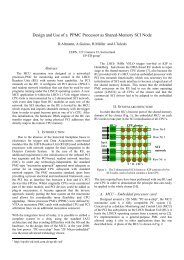
Figure 7: Block diagram <strong>of</strong> the LED triggering signals distribution<br />
board<br />
The LEDTSB board consists <strong>of</strong> the mother board and two<br />
types <strong>of</strong> the mezzanine cards: SPECS slave mezzanine for<br />
interconnection with the <strong>LHCb</strong> ECS <strong>system</strong> and Control<br />
Logic mezzanine based on radiation tolerant ACTEL FPGA.<br />
Block diagram and photo <strong>of</strong> the LEDTSB board are shown on<br />
Figure 7 and 8.<br />
LEDTSB specification<br />
• Number <strong>of</strong> channels – 64.<br />
• 16 output connectors RJ45 type on a front panel,<br />
• A level <strong>of</strong> the output signals is LVDS,<br />
• Each channel equipped with individual delay line<br />
that varies from 0 to 300 ns with 1 ns step,<br />
• A LED trigger signal width is 50 ns,<br />
• LEDTSB boards ,the same size as LFB board, will<br />
be placed in the FE crate,<br />
• Control Logic FPGA is placed on a mezzanine card<br />
for simplifying the chip exchange from non radhard<br />
to radiation hard ACTEL proASIC chip,<br />
• Memory <strong>of</strong> the scanning algorithm FPGA with 64<br />
patterns <strong>of</strong> the output trigger signals allows perform<br />
all needed sequences for LED flashing,<br />
1<br />
2<br />
16<br />
17<br />
18<br />
32<br />
33<br />
34<br />
48<br />
49<br />
50<br />
64<br />
1 - 4<br />
LVDS<br />
• SPECS slave mezzanine card (developed in LAL) is<br />
used for connection with ECS and TTCrx decoding,<br />
• There are two operational mode:<br />
A. The main mode, when the LED trigger signals<br />
are generated from TTCrx command,<br />
B. The trigger signals are generated from a build in<br />
internal generator (Freq. ~ 1 kHz).<br />
Power consumption: +3.3 V -> 0.6 A; +5 V -> 0.1 A; -5 V<br />
-> 0.16 A.<br />
Figure 8: Photo <strong>of</strong> the LED triggering signals distribution board<br />
IV. PERFORMANCE OF THE LED MONITORING<br />
SYSTEM<br />
The <strong>calorimeter</strong> <strong>monitoring</strong> <strong>system</strong> is placed on the<br />
detector in a radiation hard environment. The electronics<br />
has been designed taken into account this factor.<br />
Main characteristics <strong>of</strong> the <strong>monitoring</strong> <strong>system</strong> are<br />
mentioned below:<br />
• Precision <strong>of</strong> the PMT gain <strong>monitoring</strong> is about<br />
0.3 %.<br />
• LED stability <strong>monitoring</strong> by a PIN diode with<br />
precision <strong>of</strong> 0.1 %.<br />
• Individual time setting for each LED in range <strong>of</strong><br />
400 ns with 1 ns step.<br />
• PIN diode with amplifier is used for <strong>monitoring</strong> the<br />
LED stability itself.<br />
• Control Logic FPGA is placed on a mezzanine card<br />
and equipped with radiation hard ACTEL pro-ASIC<br />
chip APA300.