Instructions for Authors of Papers Submitted for Publication - Cern
Instructions for Authors of Papers Submitted for Publication - Cern
Instructions for Authors of Papers Submitted for Publication - Cern

You also want an ePaper? Increase the reach of your titles
YUMPU automatically turns print PDFs into web optimized ePapers that Google loves.
Design and Use <strong>of</strong> a PPMC Processor as Shared-Memory SCI Node<br />
Abstract<br />
The MCU mezzanine was designed as a networked<br />
processor-PMC <strong>for</strong> monitoring and control in the LHCb<br />
Readout Unit (RU) with remote boot capability. As PCI<br />
monarch on the RU, it configures all PCI devices (FPGA’s<br />
and readout network interface) that can then be used by user<br />
programs running under the LINUX operating system. A new<br />
MCU application is within the LHCb L1-Velo trigger where a<br />
CPU-farm is interconnected by a 2-dimensional SCI network,<br />
with event data input from RU modules at each row <strong>of</strong> the<br />
network: the SCI interface on the RU is hosted by the MCU<br />
which exports and imports shareable memory with the trigger<br />
farm in order to quasi become part as one <strong>of</strong> it’s CPU. After<br />
this initialisation, the hardware DMA engines <strong>of</strong> the RU can<br />
transfer trigger data, by using physical PCI addresses that<br />
directly map to the remote CPU memory.<br />
I. INTRODUCTION<br />
Due to the absence <strong>of</strong> the historical backplane buses in<br />
electronics <strong>for</strong> trigger and Data Acquisition, crate-based<br />
modules like the LHCb Readout Unit (RU)[8] need embedded<br />
processors with network support <strong>for</strong> their integration in the<br />
Detector Controls System. In the case <strong>of</strong> the RU, an<br />
additional requirement is the initialisation <strong>of</strong> the onboard PCI<br />
bus segments and the PCI-based, readout network interface<br />
(NIC). In order stay technology-independent, the standard<br />
PMC-type “mezzanine approach” appeared most adequate as<br />
carrier <strong>for</strong> an integrated CPU subsystem with standard<br />
network support. The PMC mezzanine standard, apart from<br />
providing a proven electrical and mechanical framework, uses<br />
the PCI bus as interface bus between a host and it’s PCI<br />
devices like FPGAs. Whilst originally CPUs were considered<br />
part <strong>of</strong> the main module, and PCI devices could be added as<br />
plug-in mezzanines, it became apparent that the inverse<br />
approach, namely putting the host system on the mezzanine<br />
card allows <strong>for</strong> considerable more flexibility and CPU<br />
upgrading. Hence processor PMCs (PPMC) were defined by<br />
VITA as mezzanine PMC cards with embedded CPU and PCI<br />
arbitration lines via an additional mezzanine connector.<br />
With the integration level <strong>of</strong> today, it is possible to embed a<br />
complete system in a chip, using the standard IA32<br />
architecture and thus avoiding difficulties with the OS and the<br />
hardware. At the design time <strong>of</strong> the MCU, in the year 2000,<br />
the low power “PC-on-a-chip” from “ZF Micro-embedded”<br />
was the most advanced technology choice.<br />
1 http://ep-div-ed.web.cern.ch/ep-div-ed/<br />
D.Altmann, A.Guirao, H.Müller and J.Toledo<br />
CERN, 1211 Geneva 23, Switzerland<br />
EP-ED group 1<br />
The LHCb 1MHz VELO trigger test-bed at KIP in<br />
Heidelberg had chosen the DMA-based RU module as input<br />
stage to the shared-memory CPU cluster [7], also because the<br />
RU provided with it’s MCU card an embedded processor with<br />
PCI bus monarch functionality which was necessary <strong>for</strong> the<br />
initialisation <strong>of</strong> SCI node interface to become a logical part <strong>of</strong><br />
the shared memory domain. This meant that the embedded<br />
PMC processor on the RU had to run the same operating<br />
system (LINUX) as all CPUs <strong>of</strong> the cluster and that the<br />
commercial SCI drivers had to be adapted to the embedded<br />
system.<br />
II. SYSTEM ARCHITECTURE<br />
In order that the RU’s become part <strong>of</strong> the shared memory<br />
domain <strong>of</strong> the cluster (Fig. 1), the embedded MCU on each<br />
RU needs to take part in the SCI initialisation <strong>of</strong> all CPU’s.<br />
Input<br />
links<br />
RU’s CPU cluster<br />
MCU<br />
MCU<br />
MCU<br />
MCU<br />
MCU<br />
N * M CPU’s<br />
Row Nr 0<br />
Row Nr 1<br />
SCI<br />
network<br />
Row Nr n<br />
Figure 1: The 2-dimensional SCI cluster at KIP consists <strong>of</strong> n*m<br />
SCI nodes, each <strong>of</strong> which contains a farm CPU.<br />
The tests reported here have been per<strong>for</strong>med with one RU and<br />
one CPU in order to demonstrate the principle that can easily<br />
be applied to the whole cluster [10].<br />
A. MCU – Embedded processor card<br />
Designed around a 120 MHz "PC-on-a-chip", the MCU<br />
mezzanine card is a fully compatible PC system [1].<br />
Conceived as a diskless Monitoring and Control Unit (MCU)<br />
<strong>of</strong> the PCI bus subsystems on the LHCb Readout Unit (RU), it<br />
boots the LINUX operating system from a remote server [2].<br />
It's implementation as a general-purpose PMC card has<br />
allowed using it also in other applications than the one<br />
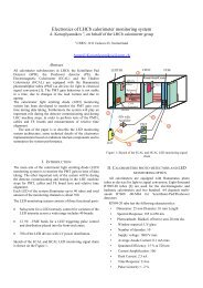
described here. A photo <strong>of</strong> the MCU is shown in Fig. 2.
Figure 2: The MCU mezzanine card (PMC <strong>for</strong>mat)<br />
The MCU's core is based on a Cyrix 486 core<br />
architecture which integrates a peripheral subsystem which is<br />
divided in two large blocks (Fig 3): embedded interfaces with<br />
PCI bus and I/O extensions. The embedded interfaces are<br />
serial and parallel ports, watchdog timers, EIDE, USB and<br />
floppy controllers, access bus (I2C compatible) interface,<br />
keyboard and PS/2 mouse systems. Extra additions to this are<br />
the 10/100 Mbit Ethernet and user programmable I/O. The<br />
latter are available via the VITA-32 user connector (P14) and<br />
used as a general JTAG port on the RU board.<br />
486<br />
CPU<br />
NORTH<br />
BRIDGE<br />
SOUTH<br />
BRIDGE<br />
BIOS<br />
ROM<br />
ETHERNET<br />
CONTROLLER<br />
FAILSAFE<br />
ROM<br />
SDRAM<br />
64 M<br />
FRONT SIDE PCI (INTERNAL)<br />
IDE<br />
CONTROLLER<br />
REMOTE<br />
BOOT PROM<br />
PARALLEL<br />
SERIAL<br />
PORTS<br />
USB<br />
CONTROLLER<br />
BACK SIDE PCI (EXTERNAL PMC) 32b@33MHz<br />
LEGACY ISA BUS (EXTERNAL PMC)<br />
KEYS<br />
& PS/2<br />
PORTS<br />
GPIO<br />
PORT<br />
ACCESS<br />
BUS<br />
(I 2 C)<br />
Figure 3: Architecture <strong>of</strong> MCU subsystems. Un-shaded blocks are<br />
integral part <strong>of</strong> the “PC-on-a-chip”.<br />
The bus architecture <strong>of</strong> the Readout Unit is depicted in<br />
Fig. 4. The MCU being a PCI monarch on the Readout Unit, it<br />
scans and initialises the PCI bus during the boot operation,<br />
finding and configuring:<br />
1. All FPGAs and their resources<br />
2. The SCI network interface card<br />
3. All buffers and registers mapped via the FPGA's<br />
After the hardware configuration, the operating system is<br />
loaded from a server that also configures the SCI network<br />
card according to the procedures defined <strong>for</strong> PCI, i.e. via<br />
access to the PCI configuration space <strong>of</strong> the SCI card.<br />
B. DMA architecture on RU<br />
The output FPGAs in each RU are connected to a 64 bit<br />
wide input buffer, each <strong>of</strong> which is filled from 2 Slink [6]<br />
input stages (Fig. 4). These input buffers are dual port RAMs,<br />
(used like a circular buffer) which are filled on one side from<br />
Slink and emptied on the other side by FPGA-based DMA<br />
engines. The RU has two parallel DMA engines, which are<br />
multiplexed via the common PCI bus. This dual data path<br />
architecture was chosen in order to increase the I/O<br />
per<strong>for</strong>mance via interleaved DMAs, where two PCI burst<br />
coming from each data path combine their payloads in a<br />
single SCI packet which gets sent to the network cluster.<br />
Figure 4: Readout Unit with MCU and SCI card. Event-fragments<br />
are received in 2 input buffers <strong>of</strong> which each has 2 Slink inputs. The<br />
two buffers are combined in the SCI card via the PCI write<br />
combining protocol: both DMA engines send their fragments in<br />
close succession to the same SCI card buffer.<br />
In order to synchronize the DMAs in all RU’s, a special<br />
twisted-pair protocol named “TAGnet” was developed [9].<br />
Via this protocol, the identifier <strong>of</strong> the next destination CPU<br />
in the cluster is received in the FPGA-resident TAGnet slave<br />
and converted into a physical PCI address <strong>for</strong> the DMA<br />
engine. The physical PCI address has been obtained through<br />
the SCI initialisation procedure <strong>of</strong> the MCU, mapping local<br />
PCI memory space into a remote CPU memory. The transport<br />
<strong>of</strong> data from the local PCI bus to the remotely mapped<br />
memory is entirely per<strong>for</strong>med by the SCI network hardware<br />
and requires only several microseconds.<br />
C. SCI Initialisation<br />
SCI is a scalable network standard [4] with a raw<br />
bandwidth <strong>of</strong> currently ca. 6 Gbit/s. SCI allows in particular<br />
implementing a shared memory paradigm between remotely<br />
connected CPUs. Interfaced via the PCI bus, SCI network<br />
bridges need to be initialised via a dedicated driver that will<br />
map remote memory segments into the local computer<br />
address space.
For the embedded applications, PMC versions <strong>of</strong> the SCI<br />
brides exist (Fig 5) from a leading manufacturer [3] <strong>of</strong> SCI<br />
technology.<br />
Figure 5: Photo <strong>of</strong> Dolphin SCI card (PMC version). SCI packets are<br />
received and transmitted via two 16 bit wide differential LVDS<br />
connectors. The PCI mezzanine connectors are configured <strong>for</strong> 64 bit<br />
and 66 MHz.<br />
III. DATA TRANSFER FROM RU TO CPU<br />
Once initialised by the MCU, the RU becomes part <strong>of</strong> the<br />
shared memory system <strong>of</strong> the CPU farm. A hardware DMA in<br />
an FPGA can directly send data to remote CPU memory by<br />
using a local physical PCI address (figure 6). Using a<br />
modified version <strong>of</strong> the IRM driver <strong>for</strong> SCI on the MCU, it<br />
exports and imports shareable memory with the other CPU<br />
nodes in the farm. The SCI adapter on the Readout Unit<br />
shares its 64 bit@66 MHz PCI bus segment with an FPGAresident<br />
DMA engine. The latter requires a physical PCI<br />
address to copy trigger data to remote, exported memory in a<br />
farm CPU node. The corresponding physical address is<br />
available after the shared memory initialization has been<br />
completed..<br />
P<br />
C<br />
I<br />
B<br />
U<br />
S<br />
DMA<br />
ENGINE<br />
FPGA<br />
DMA<br />
ENGINE<br />
FPGA<br />
PCI<br />
MEMORY<br />
SPACE<br />
SCI CARD<br />
READOUT UNIT<br />
MCU<br />
SCI BRIDGE<br />
SCI LINK<br />
PC FARM CPU<br />
SCI BRIDGE<br />
CPU<br />
STANDARD PC<br />
SCI CARD<br />
PCI<br />
MEMORY<br />
SPACE<br />
Figure 6: Data transfer between Readout Unit and CPU farm. Two<br />
alternating DMA engines in the Readout Unit transmit event-data to<br />
a mapped memory space within the SCI bridge. The SCI link<br />
transmits the combined DMAs to the PCI bus <strong>of</strong> the remote CPU.<br />
The copy process from the local PCI bus to a remote PCI bus<br />
<strong>of</strong> a CPU is similar to a hardware copy to local memory,<br />
requiring only a few microseconds. For speed enhancement,<br />
the RU uses two alternating DMA engines that write two<br />
consecutive PCI bursts to the SCI bridge. The PCI write<br />
combining protocol generates a single packet from the two<br />
inputs, hence also per<strong>for</strong>ms data multiplexing on the fly.<br />
P<br />
C<br />
I<br />
B<br />
U<br />
S<br />
D. Remotely mapped PCI address<br />
A few lines <strong>of</strong> code are needed to find the PCI physical<br />
memory address that maps to a remote CPU on the farm. It<br />
uses the IRM SCI driver layer and calls the SCIQuery<br />
function.<br />
qlseg.subcommand = SCI_Q_REMOTE_SEGMENT_IOADDR;<br />
qlseg.segment = remoteSegment;<br />
SCIQuery (SCI_Q_REMOTE_SEGMENT, &qlseg, NO_FLAGS,<br />
&error);<br />
printf("The physical address <strong>for</strong> the remote segment is : %x\n",<br />
qlseg.data.ioaddr);<br />
which will result in a screen dump like:<br />
The physical address <strong>for</strong> the remote segment is: fd040000<br />
When a CPU identifier is received via TAGnet, there is a<br />
lookup table entry that outputs its corresponding physical PCI<br />
address. The loading <strong>of</strong> the lookup table is part <strong>of</strong> the SCI<br />
initialisation procedure <strong>of</strong> the MCU.<br />
E. Results<br />
A successful integration <strong>of</strong> Readout Units into the shared<br />
memory domain <strong>of</strong> a CPU farm has been demonstrated by<br />
using the MCU card as host processor <strong>for</strong> the initialisation <strong>of</strong><br />
the SCI bridge on the RU. The initialisation <strong>of</strong> SCI via an<br />
embedded 486 -type CPU required modifications [5] to the<br />
company IRM driver that was developed <strong>for</strong> server-type<br />
CPUs.<br />
The measurement <strong>of</strong> Fig. 7 shows that the DMA engines <strong>of</strong><br />
the RU write two successive 64 byte PCI bursts to the SCI<br />
bridge. The lower trace shows that ca. 1 us later, a 128-byte<br />
SCI packet frame appears on the SCI ring. Fig. 8 shows that<br />
the same SCI packet has correctly addressed the destination<br />
CPU and unfolds here into a 128 byte PCI burst (SCI card as<br />
PCI master) which is directed to CPU memory that was<br />
mapped from the two DMAs on the Readout Unit.<br />
This measurement shows implicitly that:<br />
4. The SCI initialisation between the embedded MCU card<br />
on the RU and farm PC has been correctly established<br />
5. The PCI write combining <strong>of</strong> the two source DMA<br />
engines operates correctly and can be used <strong>for</strong> payload<br />
multiplexing<br />
6. The 128-byte payload packet requires 200 ns <strong>of</strong> an SCI<br />
link, hence could be transmitted at up to 5 MHz in the<br />
extreme case.
Figure 7: PCI and SCI frames at the Readout Unit (source side)<br />
At the destination side, a 128-byte SCI packet is reconverted<br />
into a PCI burst that is directed to the destination CPU<br />
memory (figure 8).<br />
Figure 8: SCI and PCI frames at the destination CPU (farm)<br />
The 200 ns SCI packet arrives at the PCI bus after a latency <strong>of</strong><br />
ca. 800 ns, which includes the PCI arbitration as PCI master.<br />
The destination CPU used has only a 32 bit @33 MHz PCI<br />
bus, hence can be extrapolated by a factor 4 to a farm-PC with<br />
64bit @66 MHz PCI bus. The burst duration on<br />
32bit@33MHz PCI bus is ca. 1 us, hence would be a factor 4<br />
less on a 64bit@66MHz version, i.e. 250 ns.<br />
The total PCI-to-PCI latency from Readout Unit to destination<br />
CPU can be combined from Fig.7 and Fig 8 and is 1,6 us +<br />
network cable delay.<br />
IV. CONCLUSION<br />
An embedded Monitoring and Control Unit PMC card has<br />
been designed and used as PCI bus monarch on the LHCb<br />
Readout Unit. The diskless mezzanine card boots LINUX<br />
from a server and initialises all FPGA–resident PCI bus<br />
resources. In the 1MHz VELO trigger application, the MCU<br />
has further been used to integrate the Readout Unit into the<br />
shared memory paradigm <strong>of</strong> the CPU cluster. After successful<br />
initialisation <strong>of</strong> the SCI network, the DMA hardware engines<br />
on the RU can use physical PCI addresses to copy trigger data<br />
to remotely mapped CPU memory. The transfer frequencies<br />
measured <strong>for</strong> aggregated data payloads <strong>of</strong> 128 byte are far<br />
beyond the required 1 MHz.<br />
V. REFERENCES<br />
[1] A networked mezzanine processor card, Guirao A., Toledo J.,<br />
Dominguez D., Bruder B., Muller H., Proceedings <strong>of</strong> 2001<br />
IEEE Real Time International Conference, Valencia, p. 81-84<br />
[2] MCU Monitoring Control Unit, a networked PMC processor <strong>for</strong><br />
the Readout Unit, D.Altmann,A.Guirao, H.Muller, LHCb note<br />
DAQ-2002-006<br />
http://hmuller.home.cern.ch/hmuller/RU/MCU/MCUnote2002.pdf<br />
[3] Dolphin Interconnect Solutions AS, http://<br />
www.dolphinics.com<br />
[4] IEEE Std. 1596-1992 IEEE Standard <strong>for</strong> Scalable coherent<br />
Interface, IEEE 1992, developed between IEEE groups,<br />
industry and the CERN RD24 project.<br />
http://hmuller.home.cern.ch/hmuller/rd24.htm<br />
[5] Installation <strong>of</strong> SCI-PCI adapters via an embedded CPU on<br />
Readout Units, D.Altmann, H.Muller, LHCB Note TRIG 2002xxxx<br />
(to appear )<br />
http://hmuller.home.cern.ch/hmuller/RU/SCIonRU/SCInote.pdf<br />
[6] LVDS link cards (SLINK) <strong>for</strong> multiplexers, VELO trigger and<br />
other applications in LHCb, F.Bal, H.Muller, LHCb DAQ 2002-<br />
005<br />
http://hmuller.home.cern.ch/hmuller/RU/Links/Slinknote.pdf<br />
[7] Architecture and Prototype <strong>of</strong> a Real-Time Processor Farm<br />
Running at 1 MHz, Inaugural doctoral thesis, Alexander<br />
Walsch, Sept 2002, KIP Heidelberg ( to appear )<br />
[8] Study and Design <strong>of</strong> the Readout Unit Module <strong>for</strong> the LHCb<br />
Experiment, Doctoral Thesis, Jose Francisco Toledo, University<br />
<strong>of</strong> Valencia, Gandia, 2001<br />
http://hmuller.home.cern.ch/hmuller/RU/curro_thesis.pdf<br />
[9] TAGnet a twisted-pair protocol <strong>for</strong> event-coherent DMA<br />
transfers in trigger farms, Hans Műller, Francois Bal, Sebastien<br />
Gonzalve, Angel Guirao, Filipe Vinci dos Santos, presented at<br />
the 8th Workshop on Electronics <strong>for</strong> LHC Experiments, Sept.<br />
2002 Colmar, France<br />
http://hmuller.home.cern.ch/hmuller/RU/TAGnet/Colmartalk.pdf<br />
[10] HS Project, horizontal slice <strong>of</strong> the Level-1 VELO Trigger, Hans<br />
Muller, Filipe Vinci dos Santos, Angel Guirao, Sebastien<br />
Gonzalv, LHCb TRIG note 2002-xxxx (to appear)<br />
http://hmuller.home.cern.ch/hmuller/RU/L1Velo/HorizontalSlic<br />
e/HSproject.pdf