L64118 MPEG-2 Transport Controller with Embedded MIPS CPU ...
L64118 MPEG-2 Transport Controller with Embedded MIPS CPU ...
L64118 MPEG-2 Transport Controller with Embedded MIPS CPU ...

Create successful ePaper yourself
Turn your PDF publications into a flip-book with our unique Google optimized e-Paper software.
<strong>L64118</strong> <strong>MPEG</strong>-2 <strong>Transport</strong><br />
<strong>Controller</strong> <strong>with</strong><br />
<strong>Embedded</strong> <strong>MIPS</strong> <strong>CPU</strong> (TR4101)<br />
Preliminary Datasheet<br />
LSI Logic’s <strong>L64118</strong> <strong>MPEG</strong>-2 <strong>Transport</strong> <strong>Controller</strong> <strong>with</strong> <strong>Embedded</strong> <strong>MIPS</strong><br />
<strong>CPU</strong> (TR4101) is a highly integrated set-top box control and<br />
communication device, combining most of the logic needed for a digital<br />
broadcast system (DBS) or cable set-top box onto a single chip. The<br />
<strong>L64118</strong>’s embedded 32-bit TinyRISC <strong>MIPS</strong> <strong>CPU</strong> core provides<br />
processing power to support transport and system data, as well as<br />
general-purpose system control.<br />
The <strong>L64118</strong> interfaces directly to LSI Logic’s L64704 and L64724<br />
(satellite), and the L64768 (cable) single-chip channel decoders, as well<br />
as to the L64105 <strong>MPEG</strong>-2 A/V decoder.<br />
The <strong>MPEG</strong>-2 transport and system demultiplexer can handle 32 Packet<br />
Identifications (PIDs) simultaneously, including audio, video, and generalpurpose<br />
data services. It integrates a Digital Video Broadcasting (DVB)compliant<br />
descrambler block, substantially increasing the security of the<br />
set-top box.<br />
The <strong>L64118</strong>’s synchronous External System Bus (EBus) communicates<br />
<strong>with</strong> external peripherals. The <strong>L64118</strong> communicates <strong>with</strong> peripherals<br />
through serial, parallel, SmartCard, and infrared ports. Several generalpurpose<br />
I/O pins are provided that let system designers expand the<br />
system’s capabilities.<br />
The <strong>L64118</strong> supports industry-standard SDRAM memory of up to<br />
16 Mbytes, using 16 and 64 Mbit SDRAMs. The SDRAM interface<br />
supports PC66/100-compliant SDRAMS.<br />
The <strong>L64118</strong> is offered in LSI Logic’s 3.3 V G10 ® -p cell-based technology<br />
and is packaged in a 256-pin PBGA (IF) package.<br />
February 1999 1<br />
Copyright © 1997, 1998 by LSI Logic Corporation. All rights reserved.<br />
®
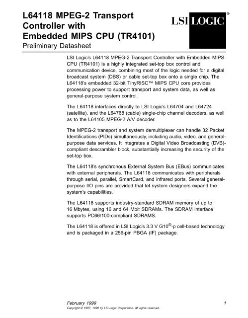
Figure 1 Typical Set-Top Box Using the <strong>L64118</strong><br />
IR Blaster/<br />
Receiver<br />
2 x<br />
SmartCards<br />
Satellite/Cable<br />
In<br />
Tuner<br />
Aux<br />
Port<br />
IEEE1284<br />
Line Driver<br />
L64724<br />
/L64768<br />
2 2<br />
Fast<br />
Parallel<br />
Port PC Modem<br />
Optional<br />
FLASH<br />
1 Mbyte x 16<br />
3 x RS232<br />
Line Driver<br />
TS<br />
External System Bus<br />
FLASH<br />
1 Mbyte x 16<br />
NTSC<br />
PAL<br />
S-VIDEO<br />
L-SPEAKER<br />
R-SPEAKER<br />
VCXO<br />
27MHz<br />
<strong>L64118</strong><br />
2 2<br />
SDRAM<br />
16 Mbyte<br />
(max.)<br />
PAL / NTSC<br />
Encoder<br />
SDRAM<br />
1 M x 16<br />
L64105<br />
CCIR601VIDEO<br />
PCM-AUDIO<br />
The <strong>L64118</strong>’s embedded 32-bit <strong>MIPS</strong> <strong>CPU</strong> (TR4101) runs at 54 MHz.<br />
The chip’s <strong>CPU</strong> block is 32 bit, while the bus interface to external<br />
memory (through the SDRAM controller) is 16 bit. The <strong>CPU</strong> can run<br />
<strong>MIPS</strong>16 and <strong>MIPS</strong>32 instructions. The 32-bit operations allow<br />
high-performance operation, while 16-bit operations allow for code<br />
optimization and memory savings. Since most transport processing and<br />
filtering is implemented in hardware, much of the <strong>CPU</strong>’s processing<br />
power can be devoted to system processing.<br />
2 <strong>L64118</strong> <strong>MPEG</strong>-2 <strong>Transport</strong> <strong>Controller</strong> <strong>with</strong> <strong>Embedded</strong> <strong>MIPS</strong> <strong>CPU</strong> (TR4101)<br />
16<br />
I 2 C<br />
Teletext<br />
Interface<br />
GP I/Os<br />
16<br />
2<br />
PCM<br />
DAC<br />
16/32<br />
2<br />
27 MHz<br />
PES<br />
Optional 1 Mbyte x 16<br />
SDRAM<br />
ACLK<br />
8<br />
16
The <strong>L64118</strong> processes the transport data packets in the PID Processing<br />
Unit (PPU) according to the <strong>MPEG</strong>-2 standard draft 13818-1, making<br />
Packetized Elementary Stream (PES), Program Specific Information<br />
(PSI), Service Information (SI), and Private data available to the system.<br />
It also buffers and transfers audio and video PES data packets to the<br />
external decoder device.<br />
The <strong>L64118</strong> interfaces directly to LSI Logic’s L64105 <strong>MPEG</strong>-2 A/V<br />
decoder. It outputs demultiplexed audio and video PES streams for<br />
processing by the L64105. This decoder’s extended channel buffer<br />
feature lets you use part of the <strong>L64118</strong> SDRAM space to store A/V PES<br />
data directed to the L64105. One benefit of this is that it lets you free<br />
memory in the L64105 and increases its On-Screen Display (OSD)<br />
capability.<br />
The <strong>L64118</strong> also interfaces directly to LSI Logic’s family of single-chip<br />
channel decoders (L64704, L64724, and L64768), which allows channel<br />
data to be transferred in parallel or serial modes. The <strong>L64118</strong><br />
implements an automatic sync locking mechanism <strong>with</strong> a programmable<br />
hysteresis function for reliable locking onto <strong>MPEG</strong>-2 (0x47) transport<br />
packet sync bytes.<br />
The External System Bus (EBus) is a general-purpose, 32-bit wide<br />
system bus. It is controlled by the <strong>L64118</strong> for communication <strong>with</strong><br />
external components in the system. This bus provides the system<br />
designer <strong>with</strong> an interface that permits the glueless connection of devices<br />
such as FLASH, ROMs, and external peripherals.<br />
The <strong>L64118</strong>’s peripheral interface blocks let you connect external<br />
systems directly to the set-top box. The RS232 ports let you connect a<br />
PC, modem, or terminal directly to the chip. The IEEE1284 parallel port<br />
lets you connect to fast peripheral devices and transfer filtered transport<br />
packets. The IEEE1284 parallel port includes an on-chip DMA controller<br />
for expediting data transfers between memory to, and from, the port.<br />
The <strong>L64118</strong> includes an infrared transmitter (blaster) port for applications<br />
such as (remotely) programming a VCR, as well as two independent<br />
infrared receiver ports, which can be used to program the set-top box<br />
using a remote controller.<br />
<strong>L64118</strong> <strong>MPEG</strong>-2 <strong>Transport</strong> <strong>Controller</strong> <strong>with</strong> <strong>Embedded</strong> <strong>MIPS</strong> <strong>CPU</strong> (TR4101) 3
Features<br />
Channel<br />
Demux<br />
The 27 MHz system clock drives the <strong>L64118</strong> internal demultiplexer block,<br />
as well as most of the peripheral modules. The PLL block generates<br />
54 MHz from the 27 MHz system clock to drive the <strong>CPU</strong> logic.<br />
The <strong>L64118</strong> includes four DMA channels (one dedicated to the<br />
IEEE1284 port, three independent) that can be used to transfer data<br />
between peripheral ports and memory, from one memory location to<br />
another, or from memory to an external system device.<br />
The <strong>L64118</strong> provides additional system features for a set-top box<br />
application, including:<br />
• Compliance <strong>with</strong> ISO/IEC 13818-1 (<strong>MPEG</strong>-2) <strong>Transport</strong><br />
specifications<br />
• Sustained rates up to 90 Mbits/s serial and up to 13.0 Mbytes/s<br />
parallel transport stream input interface<br />
• Direct interface to LSI Logic single-chip channel decoder devices,<br />
such as the L64704, the L64768, and the L64724<br />
• PID filtering (32 user-programmable PIDs)<br />
– Hardware-assisted section filtering for 30 general-purpose PIDs<br />
(PSI, SI, and Private)<br />
– Each filter includes 12 match bytes and 12 mask bytes<br />
– Each PID can select up to 32 filters simultaneously<br />
• Support of a Program Clock Reference (PCR) PID<br />
• CRC32 in parallel to all sections in the filtering process<br />
• Descrambler core compliant to DVB common scrambling<br />
specifications<br />
• Support for transport-level and PES-level descrambling<br />
• Seamless support of scrambled and unscrambled data<br />
• Support of up to 12 pairs of 64-bit keys<br />
4 <strong>L64118</strong> <strong>MPEG</strong>-2 <strong>Transport</strong> <strong>Controller</strong> <strong>with</strong> <strong>Embedded</strong> <strong>MIPS</strong> <strong>CPU</strong> (TR4101)
<strong>CPU</strong> and Subsystems<br />
• Two 256-byte transport buffers for supporting audio and video PES<br />
streams<br />
• 32 programmable cyclic buffers in SDRAM memory assignable to a<br />
PID or section filter index<br />
• Support for an additional programmable cyclic buffer in SDRAM to<br />
post data to adaptation fields<br />
• Program Clock Reference (PCR) recovery and locking<br />
• Automatic detecting and switching of audio and video PIDs on splice<br />
points<br />
• Audio oversampling (256 or 384 times oversampling) clock<br />
generation<br />
• Integration of the <strong>CPU</strong> system:<br />
– 32-bit TR4101 54 MHz TinyRISC <strong>CPU</strong><br />
– <strong>MIPS</strong>16 and <strong>MIPS</strong>-II instruction set compatible<br />
– Four Kbyte Data (direct mapped) and Eight Kbyte (two-way set<br />
associative) instruction cache<br />
– Basic Bus and Cache <strong>Controller</strong> unit (BBCC)<br />
– Multiply/Divide Unit (MDU)<br />
– Debugger Building Module (DBX)<br />
– 32-bit Timers and Interrupt <strong>Controller</strong><br />
– In-Circuit Emulator (ICE) port<br />
• Two interrupt handling modes:<br />
– Interrupt Compatibility mode supports 12 interrupt ports and six<br />
main interrupt levels. This mode is compatible <strong>with</strong> the L64108<br />
interrupt structure.<br />
– Interrupt Extension mode supports 25 interrupt ports <strong>with</strong> a<br />
software index to each interrupt source. This new mode can<br />
reduce interrupt latency.<br />
<strong>L64118</strong> <strong>MPEG</strong>-2 <strong>Transport</strong> <strong>Controller</strong> <strong>with</strong> <strong>Embedded</strong> <strong>MIPS</strong> <strong>CPU</strong> (TR4101) 5
Peripherals<br />
SDRAM <strong>Controller</strong><br />
• Programmable audio clock generator for oversampling audio DAC<br />
(ACLK)<br />
• Three RS232 serial I/O channels<br />
• IEEE1284 parallel interface port (shared <strong>with</strong> the Aux port)<br />
• Two ISO7816 SmartCard interfaces<br />
• Two Infrared (IR) receivers<br />
• One IR transmitter<br />
• Auxiliary (Aux) fast input/output port <strong>with</strong> multiple configurations and<br />
settings (shared <strong>with</strong> the IEEE1284 port)<br />
• Teletext serial interface port <strong>with</strong> direct interface to NTSC or PAL<br />
encoders<br />
• I2C-compatible interface port supporting multimaster or slave modes<br />
for interfacing to external devices<br />
• Four DMA channels (one dedicated to IEEE1284 port, three<br />
independent)<br />
• Synchronous extension bus<br />
– 32-bit external addressing<br />
– 8-/16-/32-bit data bus width<br />
– Multiplexed address/data as well as eight demultiplexed address<br />
pins<br />
– Synchronous to a 27 MHz output clock<br />
• Up to 47 general-purpose pins<br />
• Six programmable chip-select output signals (five dedicated and one<br />
multiplexed)<br />
• Enhanced serial I/O for modem use<br />
• SDRAM <strong>Controller</strong> supports 16 and 64 Mbit SDRAM devices<br />
• SDRAM <strong>Controller</strong> support for up to 16 Mbytes<br />
6 <strong>L64118</strong> <strong>MPEG</strong>-2 <strong>Transport</strong> <strong>Controller</strong> <strong>with</strong> <strong>Embedded</strong> <strong>MIPS</strong> <strong>CPU</strong> (TR4101)
General<br />
• On-chip PLL (54 MHz) <strong>with</strong> internal loop filter<br />
• JTAG support<br />
Architectural Overview<br />
• 256-pin Plastic Ball Grid Array (PBGA) Package<br />
• Commercial temperature range 0 °C–70 °C ambient<br />
• Low-power, 3.3 V (± 10%) process<br />
The components of the <strong>L64118</strong> are integrated to provide a complete<br />
system solution for demultiplexing and processing incoming <strong>MPEG</strong>-2<br />
<strong>Transport</strong> Stream packets. Figure 2 shows the three main blocks of the<br />
<strong>L64118</strong>: the TR4101 <strong>CPU</strong> and associated core building blocks, the<br />
transport (demultiplexer) block, and the peripheral device interfaces.<br />
Additionally, the <strong>L64118</strong> has three main buses:<br />
• Basic Bus (BBus)<br />
The BBus is an internal 32-bit bus that connects the <strong>CPU</strong> core and<br />
building blocks <strong>with</strong> internal memory and peripherals through the<br />
<strong>CPU</strong>-to-Peripheral (C2P) bridge.<br />
• Peripheral Bus (PBus)<br />
The PBus is the internal peripheral bus; it links the <strong>CPU</strong> to SDRAM<br />
memory, internal peripheral devices, and the demultiplexer using the<br />
C2P bridge.<br />
• External System Bus (EBus)<br />
The EBus is a general-purpose 16- and 32-bit synchronous system<br />
bus that lets the <strong>L64118</strong> communicate <strong>with</strong> external components in<br />
the system. The EBus connects to the BBus through the EBus<br />
controller.<br />
The following subsections provide an overview of the chip’s main blocks.<br />
<strong>L64118</strong> <strong>MPEG</strong>-2 <strong>Transport</strong> <strong>Controller</strong> <strong>with</strong> <strong>Embedded</strong> <strong>MIPS</strong> <strong>CPU</strong> (TR4101) 7
Figure 2 <strong>L64118</strong> Internal Block Diagram<br />
<strong>Transport</strong><br />
Stream<br />
VCx0<br />
27 MHz<br />
Register<br />
File<br />
Channel<br />
Decoder<br />
Interface<br />
PCR<br />
Clock<br />
Recovery<br />
TR4101<br />
TinyRISC<br />
Core<br />
DBX<br />
MDU<br />
Descrambler<br />
PID<br />
Processor<br />
Cache<br />
<strong>CPU</strong> Block<br />
Bus<br />
<strong>Controller</strong><br />
Cache<br />
<strong>Controller</strong><br />
BBus<br />
<strong>Transport</strong> Block<br />
Dispatcher<br />
C2P<br />
PBus<br />
Internal Peripheral Bus (PBus)<br />
SDRAM<br />
Bus<br />
Interrupt<br />
<strong>Controller</strong><br />
Timers<br />
DMA<br />
<strong>Controller</strong><br />
ICEport<br />
SDRAM<br />
<strong>Controller</strong><br />
EBus<br />
<strong>Controller</strong><br />
1284<br />
Parallel<br />
Port<br />
Aux<br />
Parallel<br />
Port<br />
I 2 C-<br />
Compatible<br />
Interface<br />
Teletext<br />
Interface<br />
SmartCard<br />
Interface<br />
Peripherals<br />
Audio<br />
Clock<br />
Generator<br />
Video PES<br />
Buffer<br />
Audio PES<br />
Buffer<br />
L64105<br />
Interface<br />
External<br />
System<br />
Bus<br />
8 <strong>L64118</strong> <strong>MPEG</strong>-2 <strong>Transport</strong> <strong>Controller</strong> <strong>with</strong> <strong>Embedded</strong> <strong>MIPS</strong> <strong>CPU</strong> (TR4101)<br />
IR<br />
Port<br />
3 Serial<br />
Ports<br />
ACLK<br />
Video<br />
Audio<br />
PES
TinyRISC <strong>MIPS</strong> <strong>CPU</strong> Core<br />
With its powerful <strong>MIPS</strong> <strong>CPU</strong>, the <strong>L64118</strong> can support all of the system’s<br />
general-purpose control requirements, including:<br />
• Complete set-top system initialization and testing<br />
• Security handling<br />
• Communication ports protocol processing<br />
• Remote control handling<br />
• PCR recovery and locking<br />
• Audio/video synchronization for lip-syncing<br />
The <strong>CPU</strong> also supports transport and system data software processing<br />
on data posted to the SDRAM by the transport processing block. This<br />
includes operations such as:<br />
• PSI and DVB SI table maintenance (Program Association Table<br />
(PAT), Conditional Access Table (CAT), Program Map Table (PMT),<br />
Network Information Table (NIT))<br />
• Private Section filtering<br />
• Subtitle processing and OSD overlay<br />
• Closed caption and teletext<br />
• Electronic Program Guide<br />
The <strong>MIPS</strong> <strong>CPU</strong> in the <strong>L64118</strong> has more than enough processing power<br />
to implement all the tasks listed above.<br />
The <strong>CPU</strong> core can be programmed <strong>with</strong> 16- or 32-bit instructions. The<br />
32-bit operations allow high-performance operation; using the 16-bit<br />
architecture permits a reduced code size, saving memory. Both 16- and<br />
32-bit instructions can be used in the same design.<br />
<strong>L64118</strong> <strong>MPEG</strong>-2 <strong>Transport</strong> <strong>Controller</strong> <strong>with</strong> <strong>Embedded</strong> <strong>MIPS</strong> <strong>CPU</strong> (TR4101) 9
The <strong>L64118</strong>’s TR4101 <strong>MIPS</strong> <strong>CPU</strong> is part of LSI Logic’s CoreWare ®<br />
technology. The chip integrates the complete <strong>CPU</strong> subsystem, including:<br />
• <strong>CPU</strong> (TR4101)<br />
• Cache memory for instruction (2 x4Kbyte) and data (4 Kbyte) cache<br />
• Basic BIU and Cache <strong>Controller</strong> (BBCC)<br />
• Timers (including watchdog timer)<br />
• Interrupt <strong>Controller</strong><br />
• Debugger Building Module (DBX)<br />
• Multiply/Divide Unit (MDU)<br />
• ICE port (full-duplex, serial receive and transmit port)<br />
• <strong>CPU</strong>-to-Peripheral bus (C2P)<br />
<strong>Transport</strong> Demultiplexer Block<br />
The <strong>L64118</strong>’s embedded 32-bit <strong>MIPS</strong> <strong>CPU</strong> runs at 54 MHz. This clock<br />
rate permits a peak processing rate of 54 <strong>MIPS</strong>. The chip’s internal <strong>CPU</strong><br />
core is implemented in 32-bit architecture, but it can execute both 16-bit<br />
and 32-bit instructions. The <strong>L64118</strong> has a 16-bit data interface to<br />
external SDRAM, and a 32-bit data interface to the external system bus<br />
(EBus). The <strong>CPU</strong> operates in Big Endian 1 mode.<br />
Since most transport processing and filtering is implemented in<br />
hardware, much of the <strong>CPU</strong>’s processing power can be devoted to<br />
system processing. The chip includes address decoding logic for directly<br />
interfacing to external memory (FLASH, SDRAM) <strong>with</strong>out requiring<br />
external glue logic.<br />
The interface between the <strong>CPU</strong> subsystem and the rest of the <strong>L64118</strong> is<br />
implemented by the C2P unit. The C2P module translates 32-bit data<br />
accesses by the <strong>CPU</strong> to 8- and 16-bit data accesses on the Peripheral<br />
Bus, which connects all other blocks. The PBus is synchronous to the<br />
27 MHz system clock.<br />
The transport demultiplexer block processes the transport stream data<br />
coming from the channel interface. The input of the <strong>L64118</strong> transport<br />
block interfaces to the channel decoder; the output interfaces to the<br />
1. Big-Endian means that the address of a multiple-byte data type is the address of its most<br />
significant byte.<br />
10 <strong>L64118</strong> <strong>MPEG</strong>-2 <strong>Transport</strong> <strong>Controller</strong> <strong>with</strong> <strong>Embedded</strong> <strong>MIPS</strong> <strong>CPU</strong> (TR4101)
SDRAM <strong>Controller</strong><br />
External System Bus (EBus)<br />
SDRAM controller module. The block includes a PID processor unit<br />
(PPU) that is compliant <strong>with</strong> DVB and JSAT and meets the requirements<br />
of many other service providers, including Canal+, SkyPerfect, and<br />
BSkyB.<br />
The unit can process up to 32 PIDs simultaneously. It provides extensive<br />
filtering of PSI, SI, and Private Sections. The PSI, SI, and Private<br />
Sections are filtered according to 32 user-programmable match/mask<br />
PIDs. Section data that passes filtering is stored in cyclic buffers (in offchip<br />
memory) associated <strong>with</strong> each PID. Each section in each PID can<br />
be filtered against 32 filters. (Every section undergoes a CRC32 check.<br />
An enable bit controls the CRC checking of all section types.) The onchip<br />
descrambler unit increases system security. The audio and video<br />
data are reduced to PES streams and delivered to the A/V decoder.<br />
The SDRAM controller and resource arbitration logic makes efficient use<br />
of SDRAM bandwidth. This chip’s low-cost system implementation<br />
approach dictates usage of the external SDRAM for both transport and<br />
general system functions. The <strong>L64118</strong> supports various SDRAM<br />
configurations using 16 Mbit and 64 Mbit devices, for a total memory size<br />
of 2, 8, or 16 Mbytes of external SDRAM.<br />
The SDRAM controller arbitrates access to the external SDRAM. This<br />
logic provides the maximum possible SDRAM bandwidth to the on-chip<br />
<strong>CPU</strong> <strong>with</strong>out increasing the need for buffers or other resources.<br />
The External System Bus is a general-purpose 16- and 32-bit system<br />
bus used for communication <strong>with</strong> external components in the system.<br />
This bus provides the system designer <strong>with</strong> an interface that permits the<br />
glueless connection of devices like FLASH, ROMs, and external<br />
peripherals.<br />
The EBus comprises a 32-bit wide interface <strong>with</strong> multiplexed address and<br />
data. Eight address bits are available as demultiplexed bits for easy<br />
interface to devices that do not need the full address space. In addition<br />
a demultiplexed mode can be configured to provide a 24-bit address and<br />
16-bit data bus.<br />
<strong>L64118</strong> <strong>MPEG</strong>-2 <strong>Transport</strong> <strong>Controller</strong> <strong>with</strong> <strong>Embedded</strong> <strong>MIPS</strong> <strong>CPU</strong> (TR4101) 11
Peripherals<br />
The EBus controller registers let the user program customized timing for<br />
each address space used in a given system. Six address spaces are<br />
supported, each <strong>with</strong> a dedicated chip select output.<br />
The main features of the EBus are:<br />
• 32-bit physical addressing space<br />
• 32-bit data width<br />
• Synchronized to 27 MHz clock<br />
• Five external interrupt ports<br />
The EBus supports the following main signals:<br />
• 32-bit multiplexed address/data<br />
• 8-bit demultiplexed (low order) address bits<br />
• RDn<br />
• WRn<br />
• EACKn<br />
• ALE (Address latch enable)<br />
• Five dedicated chip-selects and one multiplexed (<strong>with</strong> memory<br />
strobe) chip select<br />
• 4-bit byte enable bus<br />
• 27 MHz output clock<br />
The <strong>L64118</strong> integrates several serial and parallel ports, providing a high<br />
degree of connectivity to various types of peripherals. The<br />
communication ports include:<br />
• Three 8251 RS232 serial communication ports connect the set-top<br />
box to a dumb monitor, modem, or PC. The modem communicates<br />
between the subscriber and the main station, or back channel.<br />
One serial I/O includes a V24-compatible UART for a glueless<br />
connection to modem datapump ICs.<br />
12 <strong>L64118</strong> <strong>MPEG</strong>-2 <strong>Transport</strong> <strong>Controller</strong> <strong>with</strong> <strong>Embedded</strong> <strong>MIPS</strong> <strong>CPU</strong> (TR4101)
• One IEEE1284 parallel communication port for fast communication<br />
<strong>with</strong> a PC or workstation. The <strong>L64118</strong> includes an on-chip DMA<br />
controller dedicated for data transfers between the IEEE1284 parallel<br />
communication port and the main memory.<br />
• One I2C-compatible serial communication port to communicate <strong>with</strong><br />
devices using I2C data links. This type of bus is common in video<br />
encoders, audio DACs, remote control devices, and RF tuners.<br />
• Two independent SmartCard ports ISO-7816-3 compliant SmartCard<br />
ports interface through a SmartCard coupler, and support the T = 0,<br />
T = 1 asynchronous protocol. The ports also feature VCC ,VPP control.<br />
• One Teletext port that interfaces to an NTSC or PAL encoder and<br />
allows for direct insertion of teletext data into an NTSC or PAL video<br />
encoder device. The teletext data usually is transmitted using a<br />
special-purpose PID. The data is then extracted by the <strong>Transport</strong><br />
processor and posted to SDRAM. Finally, the <strong>L64118</strong> controller<br />
transfers the teletext data to the Teletext port upon request from the<br />
video encoder device. The Teletext port includes a FIFO between the<br />
real-time timing required on the output pins and the internal data<br />
transfer.<br />
• An Aux parallel port for outputting/inputting transport packets from/to<br />
the internal demultiplexer. The port’s direction is controlled through a<br />
configuration bit or through the AUXTX input pin. The port can be<br />
programmed to deliver or receive transport packets at various points<br />
<strong>with</strong>in the demultiplexer’s pipeline. This port is multiplexed <strong>with</strong><br />
signals from the IEEE1284 port.<br />
• An Infrared port <strong>with</strong> a single IR blaster <strong>with</strong> two identical output pins<br />
and two identical, yet independent, IR receiver modules. The IRT<br />
(transmitter) can be used to communicate <strong>with</strong> off-board elements<br />
(e.g., to program a VCR). The two IR receivers, IR0 and IR1, support<br />
remote control of the STB.<br />
• Forty-seven general-purpose I/O pins (GPIOs) are configurable and<br />
can be used to control and monitor a subset of processor functions,<br />
thus easing system integration and minimizing external glue logic.<br />
Forty-one of these I/Os are multiplexed, six are dedicated GPIOs.<br />
<strong>L64118</strong> <strong>MPEG</strong>-2 <strong>Transport</strong> <strong>Controller</strong> <strong>with</strong> <strong>Embedded</strong> <strong>MIPS</strong> <strong>CPU</strong> (TR4101) 13
DMA <strong>Controller</strong><br />
Addressing<br />
The <strong>L64118</strong> integrates a four-channel DMA controller that reduces a<br />
major portion of the load the <strong>CPU</strong> might incur during data transfer<br />
between peripheral ports, memory, and elements residing on the EBus.<br />
One DMA channel is dedicated for data transfers between the IEEE1284<br />
port and main memory. The other three DMA channels are generalpurpose.<br />
One general-purpose DMA channel (Channel #1) supports<br />
transfers between PBus and Ebus devices.<br />
In typical applications, one DMA channel can be assigned to a<br />
SmartCard, one channel to a serial port, and one to memory to memory<br />
data transfers.<br />
The <strong>MIPS</strong> architecture uses two types of addresses: virtual addresses<br />
(used in a program), and physical addresses (that appear on an address<br />
bus). This allows support of kernel and user modes, while combining<br />
cacheable and noncacheable addresses.<br />
Virtual addresses are partitioned into four, fixed-size segments: kuseg,<br />
kseg0, kseg1, and kseg2, according to Table 1.<br />
Table 1 Memory Segment Address Mapping<br />
Virtual <strong>CPU</strong> Address [31:29] Segment Size<br />
0b000–0b011 kuseg 2 Gbytes<br />
0b100 kseg0 (cache) 512 Mbytes<br />
0b101 kseg1 (noncache) 512 Mbytes<br />
0b110–0b111 kseg2 (not used) 1 Gbytes<br />
The kuseg addresses are accessible in user and kernel mode; they are<br />
for use by user-mode programs, while also providing direct access<br />
(requiring no system call) to those same addresses in kernel mode.<br />
Because the <strong>L64118</strong> does not have a Memory Management Unit (MMU),<br />
kuseg addresses are mapped unchanged to physical addresses. The<br />
<strong>L64118</strong> does not map kseg2; thus, kseg2 addresses cannot be used by<br />
14 <strong>L64118</strong> <strong>MPEG</strong>-2 <strong>Transport</strong> <strong>Controller</strong> <strong>with</strong> <strong>Embedded</strong> <strong>MIPS</strong> <strong>CPU</strong> (TR4101)
the programmer. Noncacheable kseg1 addresses are used for accessing<br />
peripheral registers and for code that requires noncacheability (for<br />
example, initialization code that is executed before the caches have been<br />
flushed). Cacheable kseg0 addresses are used for all other code.<br />
The on-chip <strong>CPU</strong> performs virtual to physical address translation; the<br />
resultant 32-bit physical addresses are output on the internal BBus. The<br />
<strong>CPU</strong> to Peripheral (C2P) bridge module maps the 32-bit BBus address<br />
to the internal 24-bit PBus address. The EBus interface module (which<br />
resides on the internal BBus) maps the 32-bit BBus address to the<br />
24/32 1 -bit EBus address, according to the mode in which the EBus<br />
interface is configured and the width of the area being accessed.<br />
The <strong>L64118</strong> supports a 16 or 32 Mbyte physical address space<br />
(depending on the size of the SDRAM supported in the system). Virtual<br />
addresses in kseg0 and kseg1 are always mapped to the same physical<br />
addresses, namely to the lowest 16 (or 32) Mbytes of physical memory.<br />
The programmer can differentiate between cacheable and<br />
noncacheable addresses by using a virtual address either in kseg0 or<br />
kseg1 (e.g., PSI/PES data is stored in a noncacheable location, since<br />
they are posted by the PID processor).<br />
As part of the <strong>CPU</strong> subsystem, the <strong>L64118</strong> a small module (the MMU<br />
Stub) that maps the kseg0 and kseg1 segments to the same physical<br />
address. It does this by clearing the three most significant bits of the<br />
address in the kseg0 and kseg1 segments presented by the <strong>CPU</strong> (on the<br />
internal <strong>CPU</strong> bus). Segments kuseg and kseg2 are unaffected by the<br />
MMU Stub.<br />
Note that the <strong>L64118</strong> <strong>CPU</strong> operates only in Big-Endian mode; the Ebus<br />
must be set to operate in Big-Endian mode. A strap option on the<br />
GPIO[42] pin (sampled during reset) determines the physical connection<br />
on the EBus.<br />
1. The EBus uses either a 24-bit address or a 32-bit address, depending on the address space<br />
being accessed.<br />
<strong>L64118</strong> <strong>MPEG</strong>-2 <strong>Transport</strong> <strong>Controller</strong> <strong>with</strong> <strong>Embedded</strong> <strong>MIPS</strong> <strong>CPU</strong> (TR4101) 15
The address space of the <strong>L64118</strong> is partitioned into the following areas:<br />
• <strong>CPU</strong>/Peripheral<br />
This address space contains the control and status registers for the<br />
<strong>CPU</strong> and core building blocks.<br />
• Configuration Register Space<br />
The space contains registers that define the configuration of each<br />
peripheral on the PBus. It is partitioned into 1 Kbyte segments,<br />
where each segment corresponds to the Configuration register entry<br />
for each PBus component. See Table 3.<br />
• Attribute Register Space<br />
The Attribute register space contains the Attribute register 0 for each<br />
peripheral on the PBus. This space is partitioned into 1 Kbyte<br />
segments, where each segment corresponds to the Attribute register<br />
entry for each PBus component. See Table 3.<br />
• Internal I/O<br />
The internal I/O space contains I/O registers and functions for each<br />
peripheral on the PBus. It is partitioned into 256 4 Kbyte segments,<br />
where each segment corresponds to an I/O entry for a PBus<br />
component. See Table 3.<br />
• External ROM<br />
External ROM contains the operating system, user’s application<br />
programs (kseg0), configuration code, and initialized data (kseg1).<br />
• External space for the EBus<br />
The external space is used for user-defined external memory and<br />
external devices residing on the EBus. It is divided into three<br />
subspaces, each one supporting devices <strong>with</strong> a different width (8, 16,<br />
32 bits).<br />
• Primary SDRAM<br />
The lowest 2/8/16 Mbytes of addressable space are mapped to the<br />
external SDRAM through the internal SDRAM controller. See<br />
Table 2, “PBus to EBus Address Mapping,”<br />
16 <strong>L64118</strong> <strong>MPEG</strong>-2 <strong>Transport</strong> <strong>Controller</strong> <strong>with</strong> <strong>Embedded</strong> <strong>MIPS</strong> <strong>CPU</strong> (TR4101)
Table 2 PBus to EBus Address Mapping<br />
:<br />
118 EBus PBus Address<br />
2 Mbytes SDRAM 0x0000.0000–0x1F.FFFF<br />
8 Mbytes SDRAM 0x0100.0000–0x017F.FFFF<br />
16 Mbytes SDRAM 0x0100.0000–0x01FF.FFFF<br />
Note that the PBus addresses are not driven on the EBus, but rather<br />
are routed to the SDRAM controller. The two Mbyte and eight Mbyte<br />
mode are software compatible <strong>with</strong> the L64108 code, since the<br />
External Space 2 (ES2) of the L64108 is located at PBus address<br />
0x0080.0000 (by default).<br />
Table 3 summarizes the <strong>L64118</strong> address space.<br />
Table 3 <strong>L64118</strong> Address Mapping<br />
Virtual <strong>CPU</strong> Base Address<br />
Noncache<br />
kseg1<br />
Cache<br />
kseg0<br />
BBus Base<br />
Address<br />
Address Space<br />
Name<br />
PBus/EBus<br />
Physical<br />
Base<br />
Address<br />
Size<br />
(Mbytes)<br />
0xBFFF.0000 N/A 0x1FFF.0000 <strong>CPU</strong>/Peripheral<br />
(Reserved1 )<br />
Not used 0.50<br />
0xBFF8.0000 N/A 0x1FF8.0000 Not used Not used 0.50<br />
0xBFF4.0000 N/A 0x1FF4.0000 Internal<br />
Configuration<br />
Registers<br />
0xBFF0.0000 N/A 0x1FF0.0000 Internal Attribute<br />
Registers<br />
0xF4.0000<br />
(PBus)<br />
0xF0.0000<br />
(PBus)<br />
0xBFE0.0000 N/A 0x1FE0.0000 Internal I/O 0xE0.0000<br />
(PBus)<br />
0xBFC0.0000 0x9FC0.0000 0x1FC0.0000 External ROM 0xC0.0000<br />
(EBus demux<br />
mode)<br />
0xB800.0000 2<br />
0xB400.0000 4<br />
0xB000.0000 6<br />
0x9800.0000 0x1800.0000 8-bit devices in the<br />
External Space<br />
0x9400.0000 0x1400.0000 16-bit devices in<br />
the External<br />
Space<br />
0x9000.0000 0x1000.0000 32-bit devices in<br />
the External<br />
Space<br />
0x00.0000<br />
(EBus demux<br />
mode) 3<br />
0x00.0000<br />
(EBus demux<br />
mode) 5<br />
0x1000.0000<br />
(EBus mux<br />
mode) 7<br />
0.25<br />
0.25<br />
<strong>L64118</strong> <strong>MPEG</strong>-2 <strong>Transport</strong> <strong>Controller</strong> <strong>with</strong> <strong>Embedded</strong> <strong>MIPS</strong> <strong>CPU</strong> (TR4101) 17<br />
1<br />
2<br />
≤ 64<br />
≤ 64<br />
≤ 64
Table 3 <strong>L64118</strong> Address Mapping (Cont.)<br />
Virtual <strong>CPU</strong> Base Address<br />
Noncache<br />
kseg1<br />
0xA000.0000 0x8000.0000 0x0000.0000 Primary SDRAM<br />
when 2 Mbytes of<br />
SDRAM is used<br />
Signals<br />
Cache<br />
kseg0<br />
BBus Base<br />
Address<br />
Address Space<br />
Name<br />
0xA000.0000 0x8000.0000 0x0000.0000 Primary SDRAM<br />
when 8 or<br />
16 Mbytes of<br />
SDRAM is used<br />
PBus/EBus<br />
Physical<br />
Base<br />
Address<br />
0x0000.0000<br />
(PBus)<br />
0x0100.0000<br />
(PBus)<br />
Size<br />
(Mbytes)<br />
This section describes the signals used by the <strong>L64118</strong>. Figure 3 shows<br />
the <strong>L64118</strong> non-GPIO mode signals in functional groups and Figure 4<br />
shows the <strong>L64118</strong> GPIO mode signals. The signals are described by<br />
group. Within each group, signals are listed in alphabetic order.<br />
18 <strong>L64118</strong> <strong>MPEG</strong>-2 <strong>Transport</strong> <strong>Controller</strong> <strong>with</strong> <strong>Embedded</strong> <strong>MIPS</strong> <strong>CPU</strong> (TR4101)<br />
2<br />
8or16<br />
1. These transactions do not appear on the PBus. This space is used only when the <strong>CPU</strong> accesses<br />
BBus components (BBCC, Timer, C2P, INTC, ICEport).<br />
2. Within this range, used for 8-bit devices, specific address ranges can be selected (and the mode in<br />
which they are accessed) using the Ebus address compare registers.<br />
3. Bits [23:0] of the BBus address are reflected onto the EBus Address bus for eight-bit devices.<br />
4. Within this range used for 16-bit devices, specific address ranges can be selected (and the mode<br />
in which they are accessed) using the EBus Address Compare registers.<br />
5. Bits [23:0] of the BBus address are reflected onto the EBus Address bus for 16-bit devices.<br />
6. Within this range used for 32-bit devices, specific address ranges can be selected (and the mode<br />
in which they are accessed) using the EBus Address Compare registers.<br />
7. Same address used on the EBus and BBus when 32-bit devices are accessed.
Figure 3 <strong>L64118</strong> I/O Signal Summary (Non-GPIO Modes)<br />
CCLK<br />
Channel Interface CDATA[7:0]<br />
CERRn<br />
CVALID<br />
SCLK<br />
<strong>MPEG</strong> (PCR)<br />
SDET<br />
Phase-Locked PLLVDD<br />
Loop PLLVSS<br />
External System<br />
Bus<br />
Test<br />
Signals<br />
Serial Port/<br />
ICEPort<br />
Infrared<br />
Port<br />
IRBL<br />
IRRX0<br />
IRRX1<br />
IRTX<br />
AD[31:0]<br />
ADDR[7:0]<br />
ALE<br />
BEn[3:0]<br />
<strong>CPU</strong>_CLK<br />
CSn[4:0]<br />
CSn[5]/MEMSTBn<br />
EACKn<br />
INTn[4:0]<br />
RDn<br />
WRn<br />
ECLK<br />
IDDTN<br />
ZTESTn<br />
CTSn0<br />
CTSn1/ICECLK<br />
DSRn0<br />
DTRn0<br />
RCLK<br />
RTSn0<br />
RTSn1<br />
RXD0<br />
RXD1/ICE_RX<br />
RXD2<br />
TCLK<br />
TXD0<br />
TXD1/ICE_TX<br />
TXD2<br />
I SCL<br />
SDA<br />
TTXDATA<br />
TTXREQ<br />
2C-compatible Port<br />
Teletext Port<br />
GPIO[49:48,46:45,43:42]<br />
General-Purpose I/Os<br />
<strong>L64118</strong><br />
I/O Pin<br />
Symbol<br />
SA[11:0]<br />
SBA[1:0]<br />
SBD[15:0]<br />
SCASn<br />
SDCLK<br />
SDQMH<br />
SDQML<br />
SRASn<br />
SWEn<br />
AREQn<br />
AVALID<br />
AVD[7:0]<br />
AVERRn<br />
VREQn<br />
VVALID<br />
ACLK<br />
AVDD<br />
AVSS<br />
IREF<br />
SC0_C4<br />
SC0_C8<br />
SC0_CLK<br />
SC0_DETECT<br />
SC0_I/O<br />
SC0_RSTn<br />
SC0_VCC_ENn<br />
SC0_VPP_ENn<br />
SC1_CLK<br />
SC1_DETECT<br />
SC1_I/O<br />
SC1_RSTn<br />
SC1_VCC_ENn<br />
SC1_VPP_ENn<br />
Audio/Video<br />
Decoder<br />
Port<br />
PDATA_DIR/OP_MODE[2]<br />
OP_MODE[1:0]<br />
RESETn<br />
SDRAM Interface<br />
Audio Clock<br />
Generator<br />
SmartCard0<br />
Port<br />
SmartCard1<br />
Port<br />
TCK<br />
TDI<br />
TDO<br />
IEEE1149.1<br />
TMS<br />
JTAG Port<br />
TRSTn<br />
ACKn/AUXNM<br />
AUTOFDn/AUXV<br />
BUSY/AUXSB<br />
FAULTn/AUXCLK<br />
INITn/AUXPID[2]<br />
IEEE 1284 Parallel<br />
PDATA[7:0]<br />
and Auxiliary Port<br />
PERROR/AUXPID[0]<br />
SELECT/AUXPID[1]<br />
SELECTINn/AUX_ADP/AUX_ERR<br />
STROBEn/AUX_TX<br />
Miscellaneous<br />
<strong>L64118</strong> <strong>MPEG</strong>-2 <strong>Transport</strong> <strong>Controller</strong> <strong>with</strong> <strong>Embedded</strong> <strong>MIPS</strong> <strong>CPU</strong> (TR4101) 19
Figure 4 <strong>L64118</strong> I/O Signal Summary (GPIO Mode)<br />
CCLK<br />
Channel Interface CDATA[7:0]<br />
CERRn<br />
CVALID<br />
SCLK<br />
<strong>MPEG</strong> (PCR)<br />
SDET<br />
Phase-Locked PLLVDD<br />
Loop PLLVSS<br />
Infrared<br />
Port<br />
GPIO47<br />
GPIO40<br />
GPIO41<br />
GPIO44<br />
AD[31:0]<br />
ADDR[7:0]<br />
ALE<br />
BEn[1:0]<br />
GPIO[3:2]<br />
External System <strong>CPU</strong>_CLK<br />
Bus<br />
CSn[3:0]<br />
GPIO1<br />
CSn[5]/MEMSTBn<br />
EACKn<br />
INTn[4:0]<br />
RDn<br />
WRn<br />
ECLK<br />
Test<br />
IDDTN<br />
Signals<br />
ZTESTn<br />
GPIO7<br />
CTSn1/ICECLK<br />
GPIO9<br />
GPIO8<br />
RCLK<br />
GPIO10<br />
RTSn1<br />
Serial Port/<br />
GPIO11<br />
ICEPort RXD1/ICE_RX<br />
RXD2<br />
TCLK<br />
TXD0<br />
TXD1/ICE_TX<br />
TXD2<br />
I SCL<br />
SDA<br />
GPIO13<br />
GPIO12<br />
2C-compatible Port<br />
Teletext Port<br />
GPIO[49:48,46:45,43:42]<br />
General-Purpose I/Os<br />
<strong>L64118</strong><br />
I/O Pin<br />
Symbol<br />
SA[11:0]<br />
SBA[1:0]<br />
SBD[15:0]<br />
SCASn<br />
SDCLK<br />
GPIO6<br />
SDQML<br />
SRASn<br />
SWEn<br />
AREQn<br />
AVALID<br />
AVD[7:0]<br />
AVERRn<br />
VREQn<br />
VVALID<br />
ACLK<br />
AVDD<br />
AVSS<br />
IREF<br />
SC0_C4<br />
SC0_C8<br />
GPIO33<br />
GPIO31<br />
SC0_I/O<br />
GPIO30<br />
GPIO32<br />
GPIO34<br />
GPIO38<br />
GPIO36<br />
SC1_I/O<br />
GPIO35<br />
GPIO37<br />
GPIO39<br />
TCK<br />
TDI<br />
TDO<br />
TMS<br />
TRSTn<br />
ACKn/AUXNM<br />
GPIO14<br />
GPIO15<br />
GPIO24<br />
GPIO25<br />
GPIO[23:16]<br />
GPIO26<br />
GPIO27<br />
GPIO28<br />
GPIO29<br />
Audio/Video<br />
Decoder<br />
Port<br />
PDATA_DIR/OP_MODE[2]<br />
OP_MODE[1:0]<br />
RESETn<br />
SDRAM Interface<br />
Audio Clock<br />
Generator<br />
SmartCard0<br />
Port<br />
SmartCard1<br />
Port<br />
IEEE1149.1<br />
JTAG Port<br />
IEEE 1284 Parallel<br />
and Auxiliary Port<br />
Miscellaneous<br />
20 <strong>L64118</strong> <strong>MPEG</strong>-2 <strong>Transport</strong> <strong>Controller</strong> <strong>with</strong> <strong>Embedded</strong> <strong>MIPS</strong> <strong>CPU</strong> (TR4101)
Table 4 lists the default values of the output and bidirectional signals.<br />
Note that during reset, all bidirectional signals (and some output signals)<br />
are floating.<br />
Table 4 Default Values for <strong>L64118</strong> Output and Bidirectional<br />
Signals After Reset 1<br />
Signal Default Value Notes<br />
ACKn/AUXNM not asserted<br />
ACLK inactive (LOW)<br />
AD[31:0] driving an unknown value<br />
ADDR[7:0] driving an unknown value<br />
ALE not asserted<br />
AUTOFDn/AUXV not asserted<br />
AVALID not asserted<br />
AVD[7:0] driving an unknown value<br />
AVERRn not asserted<br />
BEn[3:0] not asserted<br />
BUSY/AUXSB not asserted<br />
CSn[4:0] not asserted<br />
CSn[5]/MEMSTBn not asserted<br />
DTRn0 not asserted<br />
FAULTn/AUXSB not asserted<br />
GPIO42, 43, 45,<br />
46, 48, 49<br />
floating<br />
INITn/AUXPID[0] not asserted<br />
IRTX not asserted<br />
PDATA_DIR/<br />
OP_MODE[2]<br />
PDATA[7:0] floating<br />
drives assertion<br />
RDn not asserted<br />
<strong>L64118</strong> <strong>MPEG</strong>-2 <strong>Transport</strong> <strong>Controller</strong> <strong>with</strong> <strong>Embedded</strong> <strong>MIPS</strong> <strong>CPU</strong> (TR4101) 21
Table 4 Default Values for <strong>L64118</strong> Output and Bidirectional<br />
Signals After Reset 1 (Cont.)<br />
Signal Default Value Notes<br />
RTSn0/1 not asserted<br />
SA[11:0] driving an unknown value<br />
SBA[1:0] driving an unknown value<br />
SBD[15:0] floating<br />
SC0_C4, SC0_C8 pulled up by an external<br />
pull-up resistor<br />
SCASn not asserted<br />
SCx_CLK not asserted<br />
SCx_DETECT floating serves as an input<br />
SCx_IO pulled up by an external<br />
pull-up resistor<br />
SCx_RSTn not asserted<br />
SCx_VPP_ENn not asserted<br />
SCx_VCC_ENn not asserted<br />
SCL pulled up using an external<br />
pull-up resistor<br />
SDA pulled up using an external<br />
pull-up resistor<br />
SDCLK toggling<br />
SDQMH not asserted<br />
SDQML not asserted<br />
SRASn not asserted<br />
SWEn not asserted<br />
22 <strong>L64118</strong> <strong>MPEG</strong>-2 <strong>Transport</strong> <strong>Controller</strong> <strong>with</strong> <strong>Embedded</strong> <strong>MIPS</strong> <strong>CPU</strong> (TR4101)
Channel Interface Port<br />
Table 4 Default Values for <strong>L64118</strong> Output and Bidirectional<br />
Signals After Reset 1 (Cont.)<br />
Signal Default Value Notes<br />
TTXREQ/GPIO12 floating behaves as an input<br />
TTXDATA not asserted<br />
TXD0/2 asserted<br />
TXD1/ICE_TX<br />
VVALID not asserted<br />
WRn not asserted<br />
1. A few cycles after reset (RESETn is driven HIGH), the <strong>L64118</strong> initiates a<br />
transaction on the EBus, changing some of the default values in this table.<br />
These signals provide the physical connection to Channel Interface<br />
devices, such as LSI Logic’s L64724 or L64768. This port supports both<br />
parallel and serial connections.<br />
CCLK Channel Clock Input<br />
When CVALID is asserted HIGH, the <strong>L64118</strong> latches<br />
CDATA[7:0] on the rising edge of CCLK. In serial mode,<br />
the <strong>L64118</strong> uses only CDATA[0]. In serial mode, the<br />
maximum clock rate is 60 MHz; in parallel mode, it is<br />
13 MHz. The CCLK must toggle during reset to ensure<br />
proper reset of the channel interface block.<br />
CDATA[7:0] Channel Data Input<br />
These signals deliver channel information to the <strong>L64118</strong>.<br />
When CVALID is asserted, the chip latches the data on<br />
every rising edge of CCLK. When the <strong>L64118</strong> is in<br />
parallel input mode, all CDATA[7:0] signals deliver data.<br />
When the <strong>L64118</strong> is in serial mode, only CDATA[0]<br />
delivers data.<br />
<strong>L64118</strong> <strong>MPEG</strong>-2 <strong>Transport</strong> <strong>Controller</strong> <strong>with</strong> <strong>Embedded</strong> <strong>MIPS</strong> <strong>CPU</strong> (TR4101) 23
CERRn Channel Data Error Input<br />
This active LOW input signal indicates that an<br />
uncorrected error occurred in the preceding channel<br />
interface. When CVALID is asserted, CERRn is latched<br />
on the rising edge of CCLK.<br />
CVALID Channel Data Valid Input<br />
This active HIGH input signal indicates that CDATA[7:0]<br />
and CERRn are carrying valid data. When CVALID is<br />
asserted, a rising edge of CCLK latches the CDATA[7:0]<br />
signals into the <strong>L64118</strong>.<br />
<strong>MPEG</strong> Program Clock Reference (PCR) Recovery<br />
Phase-Locked Loop (PLL)<br />
These signals recover the Program Clock Reference (PCR). They<br />
interface to the external VCxO, which provides the 27 MHz clock to the<br />
decoder.<br />
SCLK 27 MHz System Clock Input<br />
This input provides the clock signal to the <strong>L64118</strong>. It must<br />
be driven by the external 27 MHz VCxO (the voltage<br />
control input is controlled by SDET and the external<br />
RC filter).<br />
SDET System Clock Sigma-Delta Control Voltage Output<br />
This converter output signal from a 16-bit Sigma-Delta<br />
modulator inside the <strong>L64118</strong> drives a simple low-pass<br />
filter to produce an analog control voltage to an external<br />
VCxO.<br />
These signals supply power and ground to the internal PLL, which<br />
generates the internal 54 MHz <strong>CPU</strong> clock from the external 27 MHz<br />
SCLK input. The 54 MHz internal clock is then divided by two to generate<br />
the internal 27 MHz clock used by other internal modules. Isolate the<br />
PLLVDD and the PLLVSS signals from digital noise and digital logic on<br />
the PCB using layout and bypass filtering techniques.<br />
PLLVDD PLL Analog VDD Input<br />
This provides a separate filtered 3.3 V to the PLL circuit<br />
through PLLVDD so that switching noise from the digital<br />
portion of the chip can not affect PLL stability.<br />
24 <strong>L64118</strong> <strong>MPEG</strong>-2 <strong>Transport</strong> <strong>Controller</strong> <strong>with</strong> <strong>Embedded</strong> <strong>MIPS</strong> <strong>CPU</strong> (TR4101)
External System Bus (EBus)<br />
PLLVSS PLL Analog VSS Input<br />
This provides a separate ground to the PLL circuit<br />
through PLLVSS so that switching noise from the digital<br />
portion of the chip does not affect PLL stability.<br />
The EBus comprises a 32-bit wide interface <strong>with</strong> multiplexed address and<br />
data. Eight address bits are available as demultiplexed bits for an easy<br />
interface to devices that do not need the full address space. All bus<br />
transactions are synchronous to the 27 MHz output <strong>CPU</strong>_CLK.<br />
A subset of these signals can be programmed to act as general-purpose<br />
I/O signals by setting bit [0] in the General-Purpose Mode register.<br />
AD[31:0] Multiplexed Address/Data Bus Bidirectional<br />
AD[31:0] is the multiplexed address/data bus. The<br />
<strong>L64118</strong> can be programmed to drive the full address on<br />
this bus at access start. After this address phase the bus<br />
presents write data for a write or the external device<br />
drives data on the bus in a read.<br />
ADDR[7:0] Demuxed Address Bus Output<br />
ADDR[7:0] provides eight bits of demultiplexed address<br />
bits. This bus allows some designs to remove the<br />
external address latch on the multiplexed address/data<br />
bus to hold the address throughout the transaction. The<br />
EBus uses byte addressing. All 16-bit devices must<br />
ignore ADDR[0]. All 32-bit devices must ignore<br />
ADDR[1:0].<br />
ALE Address Latch Enable Output<br />
This active HIGH signal controls the latches for<br />
demultiplexing the address from the AD bus.<br />
BEn[1:0] Byte Enables Output<br />
The four byte enable outputs are asserted during a read<br />
or write transaction on the EBus to control which of the<br />
four byte lanes are enabled. The byte lane selection is<br />
dependent on the width of the transaction (word,<br />
halfword, or byte) and the data width of the external<br />
device (32, 16, or 8 bits).<br />
<strong>L64118</strong> <strong>MPEG</strong>-2 <strong>Transport</strong> <strong>Controller</strong> <strong>with</strong> <strong>Embedded</strong> <strong>MIPS</strong> <strong>CPU</strong> (TR4101) 25
The byte enables always correspond to the same<br />
physical lines on the AD bus: BEn[1] corresponds to<br />
AD[15:8], BEn[0] to AD[7:0].<br />
BEn[2] Byte Enable Output<br />
The four byte enable outputs are asserted during a read<br />
or write transaction on the EBus to control which of the<br />
four byte lanes are enabled. The byte lane selection is<br />
dependent on the width of the transaction (word,<br />
halfword, or byte) and the data width of the external<br />
device (32, 16, or 8 bits).<br />
The byte enables always correspond to the same<br />
physical lines on the AD bus: BEn[2] corresponds to<br />
AD[23:16].<br />
GPIO2 Bidirectional<br />
BEn[2] can serve as a general-purpose I/O signal<br />
(GPIO2) by setting bit 0 in the General-Purpose Mode<br />
register.<br />
BEn[3] Byte Enable Output<br />
The four byte enable outputs are asserted during a read<br />
or write transaction on the EBus, to control which of the<br />
four byte lanes are enabled. The byte lane selection is<br />
dependent on the width of the transaction (word,<br />
halfword, or byte) and the data width of the external<br />
device (32, 16, or 8 bits).<br />
The byte enables always correspond to the same<br />
physical lines on the AD bus: BEn[3] corresponds to<br />
AD[31:24].<br />
GPIO3 Bidirectional<br />
BEn[3] can serve as a general-purpose I/O signal<br />
(GPIO4) by setting bit 0 in the General-Purpose Mode<br />
register.<br />
<strong>CPU</strong>_CLK EBus Output Clock Output<br />
This 27 MHz output clock is generated dividing the<br />
on-chip 54 MHz clock by two. This clock serves as the<br />
reference signal for all transactions on the EBus. The<br />
timing relationship between the SDCLK output clock, the<br />
27 MHz SCLK input and the 27 MHz <strong>CPU</strong>_CLK output is<br />
unknown.<br />
26 <strong>L64118</strong> <strong>MPEG</strong>-2 <strong>Transport</strong> <strong>Controller</strong> <strong>with</strong> <strong>Embedded</strong> <strong>MIPS</strong> <strong>CPU</strong> (TR4101)
CSn[3:0] Programmable Chip Selects Output<br />
Each chip select pin can be programmed to assert in a<br />
specific address area. These pins are used to select<br />
specific external devices according to on-chip address<br />
decoding. They make interfacing to various peripherals<br />
easier, as they can remove the need for external address<br />
decoders.<br />
CSn[4] Programmable Chip Select Output<br />
This pin is similar in function to the other five chip select<br />
output pins. It is used to select specific external devices<br />
according to on-chip address decoding.<br />
GPIO1 Bidirectional<br />
CSn[4] can serve as a general-purpose I/O signal<br />
(GPIO1) by setting bit 0 in the General-Purpose Mode<br />
register.<br />
CSn[5]/MEMSTBn<br />
Chip Select[5] or Memory Strobe Output<br />
This pin is similar in function to the other five chip select<br />
output pins but holds the characteristic of being able to<br />
function as the MEMSTBn (active LOW memory strobe)<br />
signal. The MEMSTBn signal is a general-purpose<br />
signal. It can be used to indicate that a memory<br />
transaction is in progress. It is asserted in both read and<br />
write cycles. The timing on this signal is programmable.<br />
EACKn Target Acknowledge Input<br />
This signal indicates to the <strong>L64118</strong> that the external<br />
device is ready to complete the current read or write<br />
cycle. The transaction will finish if both EACKn is<br />
asserted and the internal wait state generator has<br />
expired. This mechanism allows devices to extend an<br />
access beyond the number of wait states programmed for<br />
that particular address area.<br />
EACKn can be programmed to be either active HIGH or<br />
LOW, using the XPOS bit in the CEBUSMODE register.<br />
EACKn must be deasserted before the next transaction<br />
acknowledge cycle.<br />
For self-acknowledge devices, the external EACKn pin<br />
can be ignored, so the transaction completes when the<br />
wait state generator expires. This is controlled by the<br />
XACK bit in the CECFGn register.<br />
<strong>L64118</strong> <strong>MPEG</strong>-2 <strong>Transport</strong> <strong>Controller</strong> <strong>with</strong> <strong>Embedded</strong> <strong>MIPS</strong> <strong>CPU</strong> (TR4101) 27
Miscellaneous Signals<br />
INTn4 Interrupt Input<br />
This unmaskable interrupt can be used for highest priority<br />
system needs.<br />
INTn[3:0] Interrupts Input<br />
These four external interrupts can be programmed to be<br />
level- or edge-triggered sensitive. Interrupts INTn[3:0] are<br />
maskable and for general-purpose use. When the<br />
<strong>L64118</strong> receives an interrupt, the internal <strong>CPU</strong> completes<br />
the execution of the current instruction and jumps to a<br />
preprogrammed location in the memory containing the<br />
handler for this interrupt. By default, these signals are<br />
level triggered after reset.<br />
RDn Read Output<br />
The active LOW read strobe is asserted during read<br />
operations, and deasserted during writes.<br />
WRn Write Enable Output<br />
The active LOW write strobe is asserted during write<br />
operations and deasserted during reads.<br />
These general signals are not necessarily associated <strong>with</strong> a specific<br />
function or module of the <strong>L64118</strong>.<br />
OP_MODE[1:0]<br />
Operational Mode Input<br />
These signals, along <strong>with</strong> OP_MODE[2], are used as<br />
strap options to configure various LSI Logic test modes.<br />
For normal operation, configure OP_MODE[2:0] to<br />
0b000. That is, OP_MODE[1:0] should be tied LOW, and<br />
OP_MODE[2] should be pulled LOW <strong>with</strong> a 10 kΩ<br />
resistor.<br />
OP_MODE[2]/PDATA_DIR<br />
Operational Mode Input<br />
This signal is used as a strap option during reset in<br />
conjunction <strong>with</strong> the OP_MODE[1:0] pins, and must be<br />
pulled LOW <strong>with</strong> a 10 kΩ resistor for proper device<br />
operation.<br />
28 <strong>L64118</strong> <strong>MPEG</strong>-2 <strong>Transport</strong> <strong>Controller</strong> <strong>with</strong> <strong>Embedded</strong> <strong>MIPS</strong> <strong>CPU</strong> (TR4101)
Test Signals<br />
Serial Port/ICEPort<br />
Parallel Data Direction Output<br />
After reset, this signal serves as the PDATA_DIR output,<br />
which controls the parallel data bus buffers for the 1284<br />
PDATA[7:0] data lines. When the 1284 port is used as an<br />
Aux port, this pin is driven HIGH.<br />
RESETn Asynchronous Reset Input<br />
Asserting this active LOW signal resets the <strong>L64118</strong> to its<br />
power on state. To ensure a complete reset of the<br />
<strong>L64118</strong>, RESETn must be asserted for at least 16 SCLK<br />
cycles.<br />
These signals are for LSI Logic test purposes. They must be tied to a<br />
constant value in normal operational mode.<br />
ECLK Connect to VSS Input<br />
This is an LSI Logic manufacturing test pin.<br />
IDDTN Connect to VSS Input<br />
This is an LSI Logic manufacturing test pin.<br />
ZTESTn Connect to VDD Input<br />
This is an LSI Logic manufacturing test pin. It is<br />
deasserted HIGH for normal chip operation.<br />
These signals connect the <strong>L64118</strong> to an external modem, PC, terminal,<br />
or other host that includes an RS232 interface. The <strong>L64118</strong> contains<br />
three serial ports that comply <strong>with</strong> the asynchronous specification of the<br />
RS232 standard. The on-chip baud rate generators support the standard<br />
bit rate for serial communication.<br />
Three of the SIO1 signals can be configured to serve the internal ICEport<br />
module.<br />
CTSn0 Clear to Send Port 0 Input<br />
When reset LOW, this signal indicates that the external<br />
receiver is ready for data transfer through TxD0/RxD0. If<br />
the Transmit Enable bit in the SIO Command register is<br />
set HIGH when CTSn0 is reset LOW, data from the<br />
Transmit register of Port 0 is serialized through TxD0.<br />
<strong>L64118</strong> <strong>MPEG</strong>-2 <strong>Transport</strong> <strong>Controller</strong> <strong>with</strong> <strong>Embedded</strong> <strong>MIPS</strong> <strong>CPU</strong> (TR4101) 29
GPIO7 Bidirectional<br />
CTSn0 can serve as a general-purpose I/O signal<br />
(GPIO7) by setting bit 1 in the General-Purpose Mode<br />
register.<br />
CTSn1/ICECLK<br />
Clear to Send Port1 Input<br />
This pin can serve as either the Clear to Send signal of<br />
SIO1, or as the ICEport clock input for the ICEport<br />
module. The strap option on GPIO[43] controls this pin’s<br />
functionality and usage. If GPIO[43] is sampled HIGH<br />
during reset, this pin serves as CTSn1.<br />
When reset LOW, this signal indicates that the external<br />
receiver is ready for data transfer through TxD1/RxD1. If<br />
the Transmit Enable bit in the SIO Command register is<br />
set HIGH when CTSn1 is reset LOW, data from the<br />
Transmit register of Port 1 is serialized through TxD1.<br />
Serial ICE Clock Input<br />
When serial ICE mode is enabled, this pin functions as<br />
ICECLK, the synchronous ICE port clock input.<br />
DSRn0 Data Set Ready Port 0 Input<br />
When reset to LOW, this general-purpose input control<br />
signal indicates that an external terminal device is ready<br />
for data transfer. The polarity of DSRn0 is latched in<br />
Port 0 Status register for the <strong>CPU</strong> to read.<br />
GPIO9 Bidirectional<br />
DSRn0 can serve as a general-purpose I/O signal<br />
(GPIO9) by setting bit 1 in the General-Purpose Mode<br />
register.<br />
DTRn0 Data Terminal Ready Port 0 Output<br />
When this general-purpose output control signal is reset<br />
to LOW, data for the external terminal device is ready to<br />
be transmitted. DTRn0 can be set or reset by<br />
programming the DTR bit in the SIO Command register.<br />
By default, this signal is not asserted after reset.<br />
GPIO8 Bidirectional<br />
DTRn0 can serve as a general-purpose I/O signal<br />
(GPIO8) by setting bit 1 in the General-Purpose Mode<br />
register.<br />
30 <strong>L64118</strong> <strong>MPEG</strong>-2 <strong>Transport</strong> <strong>Controller</strong> <strong>with</strong> <strong>Embedded</strong> <strong>MIPS</strong> <strong>CPU</strong> (TR4101)
RCLK Receive Serial Data Clock Input<br />
This signal is used for the receive clock input in the<br />
enhanced UART mode.<br />
RTSn0 Request to Send Port 0 Output<br />
When this general-purpose, programmable control signal<br />
is reset to LOW, Port 1 is ready to send data through<br />
TxD1. This signal is set and reset by programming the<br />
RTS bit in the SIO Command register. By default, this<br />
signal is not asserted after reset.<br />
GPIO10 Bidirectional<br />
RTSn0 can serve as a general-purpose I/O signal<br />
(GPIO10) by setting bit 1 in the General-Purpose Mode<br />
register.<br />
RTSn1 Request to Send Port1 Output<br />
When this general-purpose, programmable control signal<br />
is reset to LOW, Port 1 is ready to send data through<br />
TxD1. This signal is set and reset by programming the<br />
RTS bit in the SIO Command register.<br />
RXD0 Receive Data Port 0 Input<br />
This signal provides serial data from an external RS232<br />
device. Its protocol is similar to that of TxD0. The receive<br />
baud rate can be programmed in the SIO Baud Rate<br />
register. The data received on RXD0 is latched in the<br />
Receive register of Port 0.<br />
RXD1/ICE_RX<br />
GPIO11 Bidirectional<br />
RXD0 can serve as a general-purpose I/O signal<br />
(GPIO11) by setting bit 1 in the General-Purpose Mode<br />
register.<br />
Receive Data Port 1 Input<br />
This pin serves either as the Receive port signal of SIO1,<br />
or as the ICEport receive input for the ICEport module.<br />
The strap option on GPIO[43] controls this pin’s<br />
functionality and usage. If GPIO[43] is sampled HIGH<br />
during reset, this pin serves as RXD1. In that case, this<br />
signal provides serial data from an external RS232<br />
device.<br />
<strong>L64118</strong> <strong>MPEG</strong>-2 <strong>Transport</strong> <strong>Controller</strong> <strong>with</strong> <strong>Embedded</strong> <strong>MIPS</strong> <strong>CPU</strong> (TR4101) 31
The protocol of this pin is similar to that of TxD1. The<br />
receive baud rate is determined by programming the<br />
SIO Baud Rate register. The data received on RXD1 is<br />
latched in the Receive register of Port 1. If GPIO[43] is<br />
sampled LOW during reset, then this pin serves as the<br />
receive port for the ICEport in the <strong>L64118</strong>.<br />
Receive Data - Serial ICE Port Input<br />
When the serial ICE mode is enabled, this pin functions<br />
as ICE_RX, the receive data port input.<br />
RXD2 Receive Data Port 2 Input<br />
This signal provides serial data from an external RS232<br />
device. The protocol of this pin is similar to that of TxD2.<br />
The receive baud rate is determined by programming the<br />
SIO Baud Rate register. The data received on RXD2 is<br />
latched in the Receive register of Port 2.<br />
TCLK Transmit Serial Data Clock Input<br />
This signal is used for the transmit clock in the enhanced<br />
UART mode.<br />
TXD0 Transmit Data Port 0 Output<br />
This signal outputs data in compliance <strong>with</strong> the RS232<br />
protocol’s asynchronous specification. The transmit baud<br />
rate is determined by programming the SIO Baud Rate<br />
register. Data transmitted on TXD0 comes from the<br />
Transmit register of Port 0. By default, this signal is not<br />
asserted after reset.<br />
TXD1/ICE_TX<br />
Transmit Data Port 1 Output<br />
This pin can serve as either the Transmit Data port signal<br />
of SIO1, or as the ICEport receive input for the ICEport<br />
module. The strap option on GPIO[43] controls this pin’s<br />
functionality and usage. If GPIO[43] is sampled HIGH<br />
during reset, this pin serves as TXD1.<br />
When set to TXD1, this signal outputs data in compliance<br />
<strong>with</strong> the RS232 protocol’s asynchronous specification.<br />
The data rate on this pin is determined by programming<br />
the SIO Baud Rate register. Data transmitted on TXD1<br />
comes from the Transmit register of Port 1.<br />
32 <strong>L64118</strong> <strong>MPEG</strong>-2 <strong>Transport</strong> <strong>Controller</strong> <strong>with</strong> <strong>Embedded</strong> <strong>MIPS</strong> <strong>CPU</strong> (TR4101)
SDRAM Interface<br />
Transmit Data - Serial ICEPort Output<br />
If GPIO[43] is sampled LOW during reset, this pin serves<br />
as ICE_TX, the serial ICE transmit data output port. By<br />
default, this signal is not asserted after reset.<br />
TXD2 Transmit Data Port 2 Output<br />
This signal outputs data in compliance <strong>with</strong> the RS232<br />
protocol’s asynchronous specification. The data rate on<br />
this pin is determined by programming the SIO Baud<br />
Rate register. Data transmitted on TXD2 comes from the<br />
Transmit register of Port 2. By default, this signal is not<br />
asserted after reset.<br />
The following group of signals provides the interface between the <strong>L64118</strong><br />
and external SDRAM devices. The SDRAM interface works <strong>with</strong><br />
PC66/100 compliant SDRAMs. The <strong>L64118</strong> SDRAM interface runs at 54<br />
MHz and is capable of accessing 2, 4, 8, or 16 Mbyte memory<br />
configurations using 16 Mbit or 64 Mbit devices.<br />
This interface has a 16-bit data bus (SBD[15:0]). The upper and lower<br />
byte mask signals (SDQMH and SDQML) control halfword and byte<br />
accesses. The SBA[1:0] outputs support two- and four-bank SDRAM<br />
devices. The <strong>L64118</strong> automatically performs SDRAM refreshes.<br />
The <strong>L64118</strong> does not support the Chip Select (CSn) and Clock Enable<br />
(CKE) signals. Tie these SDRAM signals active LOW and HIGH,<br />
respectively, on the SDRAM device(s) used.<br />
SA[11:0] SDRAM Address Bus Output<br />
These signals carry the 12-bit SDRAM address bus. The<br />
number of row and column address bits used is<br />
programmable in the SDRAM Configuration register.<br />
SBA[1:0] SDRAM Bank Select Output<br />
These signals allow access to SDRAM devices <strong>with</strong><br />
either two or four banks. The number of bank select bits<br />
used is programmable in the SDRAM Configuration<br />
register.<br />
<strong>L64118</strong> <strong>MPEG</strong>-2 <strong>Transport</strong> <strong>Controller</strong> <strong>with</strong> <strong>Embedded</strong> <strong>MIPS</strong> <strong>CPU</strong> (TR4101) 33
SBD[15:0] SDRAM Data Bus Bidirectional<br />
This data bus is driven by the SDRAM during a read<br />
operation, and driven by the <strong>L64118</strong> during a write<br />
operation. It is 3-stated after reset and when there are no<br />
memory accesses.<br />
SCASn Column Address Strobe Output<br />
This signal is the active LOW column address strobe. It<br />
is used in conjunction <strong>with</strong> the SRASn and SWEn outputs<br />
to form the SDRAM command.<br />
SDCLK SDRAM Clock Output<br />
This is the master SDRAM clock. All output signals are<br />
referenced to the rising edge of SDCLK. The<br />
programmable SDRAM timing parameters are expressed<br />
in SDCLK periods.<br />
SDQMH High Byte Mask Output<br />
This active HIGH signal is the high byte data mask, which<br />
controls the high byte input/output buffer of the external<br />
SDRAM. When asserted, it disables (masks) the high<br />
data byte of the SDRAM data bus.<br />
GPIO6 Bidirectional<br />
SDQMH can serve as a general-purpose I/O signal<br />
(GPIO6) by setting bit [0] in the General-Purpose Mode<br />
register.<br />
SDQML Low Byte Mask Output<br />
This active HIGH signal is the low byte data mask, which<br />
controls the low byte input/output buffer of the external<br />
SDRAM. When asserted, it disables (masks) the low data<br />
byte of the SDRAM data bus.<br />
SRASn Row Address Strobe Output<br />
This signal is the active LOW row address strobe. SRASn<br />
is used in conjunction <strong>with</strong> the SCASn and SWEn outputs<br />
to form the SDRAM command.<br />
SWEn Write Enable Output<br />
This signal is the active LOW write enable strobe. SWEn<br />
is used in conjunction <strong>with</strong> the SRASn and SCASn<br />
outputs to form the SDRAM command.<br />
34 <strong>L64118</strong> <strong>MPEG</strong>-2 <strong>Transport</strong> <strong>Controller</strong> <strong>with</strong> <strong>Embedded</strong> <strong>MIPS</strong> <strong>CPU</strong> (TR4101)
Audio/Video Decoder Port<br />
These signals provide the interface between the <strong>L64118</strong> and an external<br />
<strong>MPEG</strong>-2 Audio/Video decoder. This interface supports a seamless<br />
connection between the <strong>L64118</strong> and LSI Logic’s L64105 A/V decoders.<br />
It supports a serial data transfer rate up to 27 Mbits/s in serial mode,<br />
9 Mbytes/s in parallel mode. The actual data rate is controlled by the<br />
audio and video request signals coming out from the A/V decoder device.<br />
AREQn Audio Data Request Input<br />
When asserted, this signal indicates that the external<br />
A/V decoder is requesting the audio bit to be clocked in<br />
to the external A/V decoder. Deassertion of AREQn<br />
indicates that the A/V decoder is not ready to accept<br />
audio data.<br />
AVALID Audio Data Valid Output<br />
When asserted, this signal indicates that valid audio data<br />
is available on the AVD[7:0] bus. A LOW-to-HIGH<br />
transition of SCLK causes the audio data bit on AVD to<br />
be latched in the external A/V decoder. In serial mode,<br />
AVALID is active HIGH. In parallel mode, AVALID latches<br />
data on the rising edge. This signal is not asserted after<br />
reset.<br />
AVD[7:0] Audio Video Compressed Data Bidirectional<br />
This bus provides data to the external A/V decoder. In<br />
serial mode, AVD[0] carries the data. In parallel mode,<br />
the entire bus carries the byte-wide data. The <strong>L64118</strong><br />
outputs PES audio and video data from the on-chip<br />
buffers and SDRAM buffers through AVD[7:0]. These<br />
signals drive an unknown value after reset.<br />
AVERRn Audio Video Data Error Output<br />
When asserted, this signal indicates that there is an<br />
uncorrected error in the bit stream entering the external<br />
A/V decoder. The <strong>L64118</strong> generates AVERRn as a result<br />
of detection of discontinuity in the transport packets of the<br />
audio and/or video program being decoded. Usually, the<br />
discontinuity is the result of loss of packets from<br />
uncorrected errors. This signal is not asserted after reset.<br />
VREQn Video Data Request Input<br />
When asserted, this signal indicates that the external<br />
A/V decoder device is requesting the video bit to be<br />
<strong>L64118</strong> <strong>MPEG</strong>-2 <strong>Transport</strong> <strong>Controller</strong> <strong>with</strong> <strong>Embedded</strong> <strong>MIPS</strong> <strong>CPU</strong> (TR4101) 35
Audio Clock Generator<br />
clocked in to the external A/V decoder. Deassertion of<br />
VREQn indicates that the A/V decoder is not ready to<br />
accept video data.<br />
VVALID Video Data Valid Output<br />
When asserted, this signal indicates that valid video data<br />
is available on the AVD line. The LOW-to-HIGH transition<br />
of SCLK causes the video data bit on the AVD[7:0] bus<br />
to be latched in the external A/V decoder. In serial mode,<br />
VVALID is active HIGH. In parallel mode, VVALID latches<br />
data on the rising edge. This signal is not asserted after<br />
reset.<br />
These signals generate the oversampling audio clock, which drives the<br />
L64105 external A/V decoder and a low-cost audio DAC. The audio clock<br />
generation circuit provides oversampling audio frequencies locked to the<br />
27 MHz program clock. The fully programmable circuit supports a wide<br />
range of oversampling audio frequencies. It is implemented using<br />
advanced mixed-signal technology.<br />
ACLK Audio Clock Output<br />
ACLK provides the oversampling audio clock that drives<br />
the L64105 audio clock input and the system clock input<br />
pin of conventional stereo audio DAC. This signal is<br />
driven LOW after reset.<br />
AVDD Analog VDD 3.3 V Input<br />
AVDD provides the power voltage to the analog circuit of<br />
the audio clock generator. It must be isolated from the<br />
Digital VDD (DVDD) by a 10 μH ferrite insulator.<br />
AVSS Analog Ground Input<br />
AVSS provides the analog ground to the audio clock<br />
generator circuit. It should must be isolated from the<br />
digital ground supply (DGND).<br />
IREF Current Reference<br />
This pin must be connected as shown in Figure 5.<br />
36 <strong>L64118</strong> <strong>MPEG</strong>-2 <strong>Transport</strong> <strong>Controller</strong> <strong>with</strong> <strong>Embedded</strong> <strong>MIPS</strong> <strong>CPU</strong> (TR4101)
IEEE 1149.1 (JTAG) Port<br />
Figure 5 IREF Connection to RC Devices<br />
<strong>L64118</strong><br />
REF_DIV<br />
18<br />
FSC_CNTL 14<br />
DCO_DIV 16<br />
16.9 kΩ 1%<br />
16<br />
AVSS<br />
AVDD<br />
IREF<br />
18-bit DAC<br />
Digital<br />
FSC<br />
0.1 μF<br />
IREF<br />
27 MHz<br />
ACLK<br />
DAC<br />
Controlled<br />
Oscillator<br />
This group of signals drive the IEEE1149.1 Test Access Port (TAP).<br />
TCK Test Clock Input<br />
This is the clock pin to sample the JTAG input data.<br />
TDI Test Data In Input<br />
This line is for the JTAG input test data.<br />
TDO Test Data Out Output<br />
This line is for the JTAG output test data.<br />
TMS Test Mode Select Input<br />
This line lets you select between active and JTAG mode.<br />
When in JTAG mode, the I/Os are serialized. Active mode<br />
is for normal operation.<br />
TRSTn Test Port Reset Input<br />
When asserted LOW, this signal resets the internal JTAG<br />
controller. It does not reset the chip.<br />
<strong>L64118</strong> <strong>MPEG</strong>-2 <strong>Transport</strong> <strong>Controller</strong> <strong>with</strong> <strong>Embedded</strong> <strong>MIPS</strong> <strong>CPU</strong> (TR4101) 37
IEEE1284 Parallel Port and Auxiliary Port<br />
These signals provide a parallel connection between the <strong>L64118</strong> and an<br />
external peripheral device. The port complies to IEEE1284 standards<br />
and supports several modes. The 1284 mode is enabled when the<br />
AUX_SEL bit is reset (System Mode register, bit 4).<br />
This port also serves as an auxiliary port for receiving and transmitting<br />
transport bitstreams from various points in the on-chip demultiplexer<br />
pipeline. The Aux mode is enabled when the AUX_SEL bit is set (System<br />
Mode register, bit 4).<br />
The following list shows each pin’s functionality as an IEEE1284 port and<br />
Aux port signal. Some of these pins also can serve as general-purpose<br />
I/O pins.<br />
ACKn/AUXNM<br />
1284 - Acknowledge Output<br />
When the <strong>L64118</strong> asserts this signal, valid data is latched<br />
in the <strong>L64118</strong> IEEE1284 input register. By default, this<br />
signal is not asserted after reset.<br />
Aux - Aux No Match Output<br />
In Aux mode, this signal functions as AUXNM to indicate<br />
that the data being sent through the auxiliary port is for<br />
a transport packet that failed PID filtering.<br />
AUTOFDn/AUXV<br />
1284 - Autofeed Input<br />
In 1284 mode, this pin functions as the Autofeed input.<br />
Aux - Data Valid Bidirectional<br />
In Aux mode, this pin functions as AUXV, which is used<br />
as a qualifier indicating that the data presented on the<br />
auxiliary data bus is valid.<br />
GPIO14 Bidirectional<br />
This signal can serve as a general-purpose I/O signal<br />
(GPIO14) by setting bit 3 in the General-Purpose Mode<br />
register.<br />
38 <strong>L64118</strong> <strong>MPEG</strong>-2 <strong>Transport</strong> <strong>Controller</strong> <strong>with</strong> <strong>Embedded</strong> <strong>MIPS</strong> <strong>CPU</strong> (TR4101)
BUSY/AUXSB<br />
1284 - Peripheral Busy Bidirectional<br />
In 1284 mode, this signal functions as BUSY. When this<br />
signal is HIGH, the 1284 port is not ready for a data<br />
transfer. By default, this signal is not asserted after reset.<br />
Aux - Sync Byte Bidirectional<br />
In Aux mode, this signal functions as AUXSB to indicate<br />
that the data being sent through the auxiliary port is the<br />
first byte (sync byte) of a transport packet.<br />
GPIO15 Bidirectional<br />
This signal can serve as a general-purpose I/O signal<br />
(GPIO15) by setting bit 3 in the General-Purpose Mode<br />
register.<br />
FAULTn/AUXCLK<br />
1284 - Peripheral Fault Operation Bidirectional<br />
In 1284 mode, this signal functions as FAULTn. This<br />
signal indicates that the 1284 port encountered an error<br />
during operation. Typically, this error is due to overrun,<br />
underrun, or parity error.<br />
Aux - Aux Port Clock Bidirectional<br />
In Aux mode, this signal functions as AUXCLK, which is<br />
the reference clock for all transactions on the auxiliary<br />
port. When the Aux port is configured as an output port,<br />
this signal is an output <strong>with</strong> programmable frequencies of<br />
13.5, 6.75 and 3.375 MHz. When the Aux port is<br />
configured as an input port, this signal is an input <strong>with</strong> a<br />
frequency based on the input transport stream data rate.<br />
GPIO24 Bidirectional<br />
This signal can also serve as a general-purpose I/O<br />
signal (GPIO24) by setting bit 3 in the General-Purpose<br />
Mode register.<br />
INIT/AUXPID[2]<br />
1284 - Peripheral Initialization Input<br />
In 1284 mode, this signal functions as INITn. When reset<br />
LOW, this signal resets the IEEE1284 port and returns<br />
the logic to the compatibility and idle state.<br />
<strong>L64118</strong> <strong>MPEG</strong>-2 <strong>Transport</strong> <strong>Controller</strong> <strong>with</strong> <strong>Embedded</strong> <strong>MIPS</strong> <strong>CPU</strong> (TR4101) 39
Aux - Packet ID [2] Output<br />
In Aux mode, this signal is part of a three-bit packet ID<br />
that can be assigned to PIDs that are output to the Aux<br />
port.<br />
GPIO25 Bidirectional<br />
This signal can also serve as a general-purpose I/O<br />
signal (GPIO25) by setting bit 3 in the General-Purpose<br />
Mode register.<br />
PDATA[7:0] Parallel I/O Data Signals<br />
1284 Bidirectional<br />
In 1284 mode, these signals carry the data transferred<br />
between the host and the IEEE1284 port.<br />
Aux Bidirectional<br />
In Aux mode, PDATA[7:0] carry the transport packets<br />
from/to the <strong>L64118</strong> demultiplexer and the Aux port.<br />
GPIO[23:16] Bidirectional<br />
These signals can also serve as a general-purpose I/O<br />
bus (GPIO[23:16]) by setting bit 3 in the General-Purpose<br />
Mode register.<br />
By default, this signal is not asserted after reset.<br />
PDATA_DIR/OP_MODE[2]<br />
1284 - Peripheral Data Direction Output<br />
After reset, this signal serves as the PDATA_DIR output<br />
signal that controls the parallel data bus buffers in 1284<br />
mode. In Aux mode, this pin is driven HIGH.<br />
Operational Mode 2 Input<br />
This signal is used as a strap option during reset. For<br />
normal device operation, use a 10 kΩ to pull this signal<br />
LOW during reset.<br />
PERROR/AUXPID[0]<br />
1284 - Peripheral Error Output<br />
In 1284 mode, this signal functions as PERROR. When<br />
HIGH, this signal indicates that the <strong>L64118</strong> IEEE1284<br />
port encountered an error during the data processing.<br />
FAULTn is asserted whenever PERROR is activated.<br />
40 <strong>L64118</strong> <strong>MPEG</strong>-2 <strong>Transport</strong> <strong>Controller</strong> <strong>with</strong> <strong>Embedded</strong> <strong>MIPS</strong> <strong>CPU</strong> (TR4101)
Aux - Packet ID [0] Output<br />
In Aux mode, this signal is part of a three-bit packet ID<br />
that can be assigned to PIDs that are output to the Aux<br />
port.<br />
GPIO26 Bidirectional<br />
This signal can also serve as a general-purpose I/O<br />
signal (GPIO26) by setting bit 3 in the General-Purpose<br />
Mode register.<br />
SELECT/AUXPID[1]<br />
1284 - Peripheral Select Output<br />
When set HIGH, this signal indicates that the <strong>L64118</strong><br />
IEEE1284 port was selected and is connected to the<br />
host.<br />
Aux - Packet ID [1] Output<br />
In Aux mode, this signal is part of a three-bit packet ID<br />
that can be assigned to PIDs that are output to the aux<br />
port.<br />
GPIO27 Bidirectional<br />
This signal can also serve as a general-purpose I/O<br />
signal (GPIO27) by setting bit 3 in the General-Purpose<br />
Mode register.<br />
SELECTINn/AUX_ADP/AUX_ERR<br />
1284 - Peripheral Selection Indicator Input<br />
In 1284 mode, this signal (when asserted LOW) indicates<br />
that the external host is attempting to select a peripheral.<br />
Aux - Adaptation Field Flag Output<br />
In Aux output mode, this signal functions as AUX_ADP,<br />
which indicates if the output byte is part of an adaptation<br />
field.<br />
Aux - Error Indicator Input<br />
In Aux input mode, this signal functions as AUX_ERR,<br />
which indicates if the incoming byte is part of a packet<br />
that has an error.<br />
GPIO28 Bidirectional<br />
This signal can also serve as a general-purpose I/O<br />
signal (GPIO28) by setting bit 3 in the General-Purpose<br />
Mode register.<br />
<strong>L64118</strong> <strong>MPEG</strong>-2 <strong>Transport</strong> <strong>Controller</strong> <strong>with</strong> <strong>Embedded</strong> <strong>MIPS</strong> <strong>CPU</strong> (TR4101) 41
I 2 C-Compatible Port<br />
STROBEn/AUX_TX<br />
1284 - Data Strobe Input<br />
In 1284 mode, this signal functions as STROBEn. When<br />
set LOW, this signal indicates that valid data is present<br />
on PDATA[7:0]. <strong>L64118</strong> latches the data on the rising<br />
edge of STROBEn.<br />
Aux - Aux Port Direction Input<br />
In Aux mode, this signal is used to specify the direction<br />
of the aux port if the PINACT bit (bit 4) is set in the Aux<br />
Control register. If AUX_TX is HIGH, then the Aux port is<br />
an output. If AUX_TX is LOW, then the Aux port is an<br />
input.<br />
GPIO29 Bidirectional<br />
This signal can also serve as a general-purpose I/O<br />
signal (GPIO29) by setting bit 3 in the General-Purpose<br />
Mode register.<br />
These signals connect the <strong>L64118</strong> to an external I 2 C device. The <strong>L64118</strong><br />
uses them to initialize external devices in the system that have this<br />
interface.<br />
SCL Serial Clock Bidirectional<br />
SCL provides the clock signal for transmitting and<br />
receiving data through SDA.<br />
SDA Serial Data Bidirectional<br />
SDA provides the data connection to the I 2 C-compatible<br />
port. Data is transmitted and received through this line<br />
according to the I 2 C protocol. This signal should be<br />
pulled HIGH by an external pull-up resistor.<br />
42 <strong>L64118</strong> <strong>MPEG</strong>-2 <strong>Transport</strong> <strong>Controller</strong> <strong>with</strong> <strong>Embedded</strong> <strong>MIPS</strong> <strong>CPU</strong> (TR4101)
Teletext Port<br />
SmartCard Port<br />
These signals connect the <strong>L64118</strong> to an external NTSC/PAL video<br />
encoder <strong>with</strong> a Teletext port.<br />
TTXDATA Teletext Data<br />
Master Output<br />
This signal supplies the teletext data to the external video<br />
encoder. The <strong>L64118</strong> outputs teletext data when<br />
TTXREQ is asserted and there are enough bits in the<br />
teletext output buffer to supply one complete teletext line.<br />
By default, this signal is not asserted after reset.<br />
GPIO13 Bidirectional<br />
TTXDATA can serve as a general-purpose I/O signal<br />
(GPIO13) by setting bit 2 in the General-Purpose Mode<br />
register.<br />
TTXREQ Teletext Data Request<br />
Master Input<br />
When set HIGH, this signal indicates that the external<br />
video encoder device requests teletext data to be<br />
transferred through TTXDATA. The <strong>L64118</strong> outputs<br />
teletext data on the TTXDATA pin as long as TTXREQ is<br />
asserted. You must program the Video Encoder device so<br />
the length of assertion of TTXREQ is compatible <strong>with</strong> the<br />
exact number of teletext bits per line. The <strong>L64118</strong><br />
Teletext port supports a direct connection to the Teletext<br />
port of NTSC/PAL video encoders. During normal operation,<br />
this is an input signal. By default, this signal is not<br />
asserted after reset.<br />
GPIO12 Bidirectional<br />
TTXREQ can serve as a general-purpose I/O signal<br />
(GPIO12) by setting bit 2 in the General-Purpose Mode<br />
register.<br />
These signals provide the connection between the <strong>L64118</strong> and external<br />
SmartCard devices. These signals are used by the <strong>L64118</strong> to initialize<br />
external devices in a system <strong>with</strong> such a port. The <strong>L64118</strong> supports two<br />
independent SmartCard devices.<br />
<strong>L64118</strong> <strong>MPEG</strong>-2 <strong>Transport</strong> <strong>Controller</strong> <strong>with</strong> <strong>Embedded</strong> <strong>MIPS</strong> <strong>CPU</strong> (TR4101) 43
SC0_C4 SmartCard 0 Pin 4 Bidirectional<br />
This signal is connected to the C4 pin on the SmartCard.<br />
This signal should be pulled up by an external pull-up<br />
resistor after reset.<br />
SC0_C8 SmartCard 0 Pin 8 Bidirectional<br />
This signal is connected to the C8 pin on the SmartCard.<br />
This signal should be pulled up by an external pull-up<br />
resistor after reset.<br />
SC0_CLK SmartCard 0 Clock Output<br />
This signal is the output clock for SmartCard 0.<br />
SC0_DETECT<br />
GPIO33 Bidirectional<br />
SC0_CLK can serve as a general-purpose I/O signal<br />
(GPIO33) by setting bit 4 in the General-Purpose Mode<br />
register.<br />
By default, this signal is not asserted after reset.<br />
SmartCard 0 Detect Input<br />
When HIGH, this signal indicates that a card is inserted<br />
in slot 0.<br />
GPIO31 Bidirectional<br />
SC0_DETECT can serve as a general-purpose I/O signal<br />
(GPIO31) by setting bit 4 in the General-Purpose Mode<br />
register.<br />
By default, this signal floats after reset.<br />
SC0_I/O SmartCard 0 I/O Bidirectional<br />
This signal transfers data (using the coupler) between<br />
SmartCard 0 and the SmartCard port of the <strong>L64118</strong>. It is<br />
open-drain. This signal must be pulled up by an external<br />
resistor after reset.<br />
SC0_RSTn SmartCard 0 Reset Output<br />
This signal resets SmartCard 0.<br />
GPIO30 Bidirectional<br />
SC0_RSTn can serve as a general-purpose I/O signal<br />
(GPIO30) by setting bit 4 in the General-Purpose Mode<br />
register.<br />
By default, this signal is not asserted after reset.<br />
44 <strong>L64118</strong> <strong>MPEG</strong>-2 <strong>Transport</strong> <strong>Controller</strong> <strong>with</strong> <strong>Embedded</strong> <strong>MIPS</strong> <strong>CPU</strong> (TR4101)
SC0_VCC_ENn<br />
SmartCard 0 VCC Enable Output<br />
This signal turns the power supply of SmartCard 0 on or<br />
off. When LOW, it enables the VCC supply.<br />
GPIO32 Bidirectional<br />
SC0_VCC_ENn can serve as a general-purpose I/O<br />
signal (GPIO32) by setting bit 4 in the General-Purpose<br />
Mode register.<br />
By default, this signal is not asserted after reset.<br />
SC0_VPP_ENn<br />
SmartCard 0 VPP Enable Output<br />
This signal turns the power supply of SmartCard 0 on or<br />
off. When LOW, it enables the VCC supply.<br />
GPIO34 Bidirectional<br />
SC0_VPP_ENn can serve as a general-purpose I/O<br />
signal (GPIO34) by setting bit 4 in the General-Purpose<br />
Mode register.<br />
By default, this signal is not asserted after reset.<br />
SC1_CLK SmartCard 1 Clock Output<br />
This signal clocks the output of SmartCard1.<br />
SC1_DETECT<br />
GPIO38 Bidirectional<br />
SC1_CLK can serve as a general-purpose I/O signal<br />
(GPIO38) by setting bit 5 in the General-Purpose Mode<br />
register.<br />
By default, this signal is not asserted after reset.<br />
SmartCard 1 Detect Input<br />
When HIGH, this signal indicates that a card is inserted<br />
in slot 1.<br />
GPIO36 Bidirectional<br />
SC1_CLK can serve as a general-purpose I/O signal<br />
(GPIO36) by setting bit 5 in the General-Purpose Mode<br />
register.<br />
By default, this signal floats after reset.<br />
<strong>L64118</strong> <strong>MPEG</strong>-2 <strong>Transport</strong> <strong>Controller</strong> <strong>with</strong> <strong>Embedded</strong> <strong>MIPS</strong> <strong>CPU</strong> (TR4101) 45
SC1_I/O SmartCard 1 I/O Bidirectional<br />
This signal transfers the data (using the coupler) between<br />
SmartCard1 and the SmartCard port of the <strong>L64118</strong>. It is<br />
open-drain. This signal must be pulled up by an external<br />
resistor after reset.<br />
SC1_RSTn SmartCard 1 Reset Output<br />
This signal resets SmartCard1.<br />
GPIO35 Bidirectional<br />
SC1_RSTn can serve as a general-purpose I/O signal<br />
(GPIO35) by setting bit 5 in the General-Purpose Mode<br />
register.<br />
By default, this signal is not asserted after reset.<br />
SC1_VCC_ENn<br />
SmartCard 1 VCC Enable Output<br />
This signal turns the power supply of SmartCard1 on or<br />
off. When LOW, it enables the VCC supply.<br />
GPIO37 Bidirectional<br />
SC1_VCC_ENn can serve as a general-purpose I/O<br />
signal (GPIO37) by setting bit 5 in the General-Purpose<br />
Mode register.<br />
By default, this signal is not asserted after reset.<br />
SC1_VPP_ENn<br />
SmartCard 1 VPP Enable Output<br />
This signal turns the power supply of SmartCard 0 on or<br />
off. When LOW, it enables the VPP pin.<br />
GPIO39 Bidirectional<br />
SC1_VPP_ENn can serve as a general-purpose I/O<br />
signal (GPIO39) by setting bit 4 in the General-Purpose<br />
Mode register.<br />
By default, this signal is not asserted after reset.<br />
46 <strong>L64118</strong> <strong>MPEG</strong>-2 <strong>Transport</strong> <strong>Controller</strong> <strong>with</strong> <strong>Embedded</strong> <strong>MIPS</strong> <strong>CPU</strong> (TR4101)
Infrared Port<br />
These signals provide the connection between the <strong>L64118</strong> and an<br />
external infrared receiver and transmitter.<br />
IRBL Infrared Blaster Output<br />
This signal is the infrared blaster output. This signal can<br />
be configured to reflect the value of the infrared<br />
transmitter output.<br />
GPIO47 Bidirectional<br />
IRBL can serve as a general-purpose I/O signal<br />
(GPIO47) by setting bit 7 in the General-Purpose Mode<br />
register.<br />
By default, this signal floats after reset.<br />
IRRX0 Infrared Receiver 0 Input<br />
This signal serves as the receive port for the<br />
demodulated signal of one of the two infrared receivers<br />
ports.<br />
GPIO40 Bidirectional<br />
IRRX0 can serve as a general-purpose I/O signal<br />
(GPIO40) by setting bit 7 in the General-Purpose Mode<br />
register.<br />
By default, this signal floats after reset.<br />
IRRX1 Infrared Receiver 1 Input<br />
This signal serves as the receive port for the<br />
demodulated signal of one of the two infrared receivers<br />
ports.<br />
GPIO41 Bidirectional<br />
IRRX1 can serve as a general-purpose I/O signal<br />
(GPIO41) by setting bit 7 in the General-Purpose Mode<br />
register.<br />
By default, this signal floats after reset.<br />
<strong>L64118</strong> <strong>MPEG</strong>-2 <strong>Transport</strong> <strong>Controller</strong> <strong>with</strong> <strong>Embedded</strong> <strong>MIPS</strong> <strong>CPU</strong> (TR4101) 47
General-Purpose Pins<br />
IRTX Infrared Transmitter Output<br />
This signal serves as the infrared transmitter output.<br />
GPIO44 Bidirectional<br />
IRRX1 can serve as a general-purpose I/O signal<br />
(GPIO44) by setting bit 7 in the General-Purpose Mode<br />
register.<br />
By default, this signal floats after reset.<br />
The general-purpose I/O signals for the <strong>L64118</strong> let you control and<br />
monitor various external events. These signals consist of eight groups.<br />
Group 7 contains dedicated GPIO signals, whereas the other groups<br />
multiplex the GPIO signals <strong>with</strong> other functions. Note that all pins <strong>with</strong>in<br />
a GPIO group must be enabled or disabled as a group; however,<br />
individual GPIO pins can be configured as inputs or outputs using the<br />
General-Purpose Control register. The GPIO groups and associated pins<br />
are listed in Table 5 through Table 12.<br />
Table 5 Group 1: EBus Signals<br />
Pin Name GPIO Signal 1<br />
CSn[4] GPIO1<br />
BEn[2] GPIO2<br />
BEn[3] GPIO4<br />
SDQMH GPIO6<br />
1. The GPIO3 and GPIO5 signals are not<br />
available on the <strong>L64118</strong>.<br />
48 <strong>L64118</strong> <strong>MPEG</strong>-2 <strong>Transport</strong> <strong>Controller</strong> <strong>with</strong> <strong>Embedded</strong> <strong>MIPS</strong> <strong>CPU</strong> (TR4101)
Table 6 Group 2: SIO Signals<br />
Pin Name GPIO Signal<br />
CTSn0 GPIO7<br />
DTRn0 GPIO8<br />
DSRn0 GPIO9<br />
RTSn0 GPIO10<br />
RXDn0 GPIO11<br />
Table 7 Group 3: Teletext Signals<br />
Pin Name GPIO Signal<br />
TTXREQ GPIO12<br />
TTXDATA GPIO13<br />
Table 8 Group 4: PIO (IEEE 1284) Signals<br />
Pin Name GPIO Signal<br />
AUTOFDn GPIO14<br />
BUSY GPIO15<br />
PDATA[7:0] GPIO[23:16]<br />
FAULTn GPIO24<br />
INITn GPIO25<br />
PERROR GPIO26<br />
SELECT GPIO27<br />
SELECTINn GPIO28<br />
STROBEn GPIO29<br />
<strong>L64118</strong> <strong>MPEG</strong>-2 <strong>Transport</strong> <strong>Controller</strong> <strong>with</strong> <strong>Embedded</strong> <strong>MIPS</strong> <strong>CPU</strong> (TR4101) 49
Table 9 Group 5: SmartCard 0 Signals<br />
Pin Name GPIO Signal<br />
SC0_RSTn GPIO30<br />
SC0_DETECT GPIO31<br />
SC0_VCC_EN GPIO32<br />
SC0_CLK GPIO33<br />
SC0_VPP_ENn GPIO34<br />
Table 10 Group 6: SmartCard 1 Signals<br />
Pin Name GPIO Signal<br />
SC1_RSTn GPIO35<br />
SC1_DETECT GPIO36<br />
SC1_VCC_ENn GPIO37<br />
SC1_CLK GPIO38<br />
SC1_VPP_ENn GPIO39<br />
Table 11 Group 8: Infrared Signals<br />
Pin Name GPIO Signal<br />
IRRX0 GPIO[40]<br />
IRRX1 GPIO[41]<br />
IRTX GPIO[44]<br />
IRBL GPIO[47]<br />
50 <strong>L64118</strong> <strong>MPEG</strong>-2 <strong>Transport</strong> <strong>Controller</strong> <strong>with</strong> <strong>Embedded</strong> <strong>MIPS</strong> <strong>CPU</strong> (TR4101)
GPIO[49, 48, 46, 45, 43, 42]<br />
Dedicated GPIO Bidirectional<br />
These are the dedicated general-purpose I/O signals. By<br />
default, these signals float after reset. Note that for<br />
LSI Logic manufacturing test purposes, GPIO46 must be<br />
pulled HIGH during reset.<br />
Programming the General-Purpose Pins<br />
Latency of GPIO Updates<br />
Table 12 Group 7: Dedicated GPIO Signals<br />
Pin Name GPIO Signal<br />
GPIO[43:42] GPIO[43:42]<br />
GPIO[46:45] GPIO[46:45]<br />
GPIO[49:48] GPIO[49:48]<br />
To use a general-purpose pin, enable the entire group by writing to the<br />
General-Purpose Mode register; then select the input/output for each pin<br />
<strong>with</strong>in the group by writing to the specific General-Purpose Control<br />
register. (Note that no group has more than 16 general-purpose pins.)<br />
After each pin is defined, the programmer can read the value of the<br />
GPIO signal using the General-Purpose Data registers, or write the value<br />
of a GPIO signal to the General-Purpose Data registers.<br />
The use of the GPIO pins is intended for controlling/monitoring external<br />
logic by the software.<br />
You should consider a delay between the time when the software writes<br />
a value to a general-purpose output pin and the time the value is valid<br />
on the output pin. This delay is caused by the transaction time between<br />
the on-chip processor to the on-chip peripheral component, and the<br />
delay time of the general-purpose module.<br />
The delay that the general-purpose module inserts in writing to an output<br />
general-purpose pin is not more than 1 μs (for SCLK = 27 MHz).<br />
<strong>L64118</strong> <strong>MPEG</strong>-2 <strong>Transport</strong> <strong>Controller</strong> <strong>with</strong> <strong>Embedded</strong> <strong>MIPS</strong> <strong>CPU</strong> (TR4101) 51
Electrical Requirements<br />
When the processor reads a value from a general-purpose pin<br />
configured to be an input pin, there is no extra delay inserted; however,<br />
the register holding general-purpose input values is updated every 2 μs<br />
(for SCLK = 27 MHz).<br />
This section specifies the electrical requirements for the <strong>L64118</strong>. Five<br />
tables list electrical data in the following categories:<br />
• Absolute Maximum Ratings (Table 13)<br />
• Recommended Operating Conditions (Table 14)<br />
• Capacitance (Table 15)<br />
• DC Characteristics (Table 16)<br />
• Pin Description Summary (Table 17)<br />
The following tables provide the maximum ratings, operating conditions,<br />
and capacitances for the 3.3 V, G10-p implementation of the <strong>L64118</strong>.<br />
Table 13 Absolute Maximum Ratings<br />
Symbol Parameter Limits 1<br />
V DD DC Supply − 0.3 to + 3.9 V<br />
V IN 5 V Compatible Input Voltage − 1.0 to 6.0 V<br />
V IN 3.3 V Input Voltage − 0.8 to 4.7 V<br />
TSTGP Storage Temperature Range<br />
(Plastic)<br />
1. Referenced to VSS .<br />
52 <strong>L64118</strong> <strong>MPEG</strong>-2 <strong>Transport</strong> <strong>Controller</strong> <strong>with</strong> <strong>Embedded</strong> <strong>MIPS</strong> <strong>CPU</strong> (TR4101)<br />
Unit<br />
I IN DC Input Current ± 10 mA<br />
− 40 to + 125 °C
Table 14 Recommended Operating Conditions<br />
Symbol Parameter Limits Unit<br />
V DD DC Supply + 3.0 to + 3.6 V<br />
T A Ambient Temperature 0 to + 70 °C<br />
Table 15 Capacitance<br />
Symbol Parameter 1<br />
Min Typ Max Units<br />
C IN Input Capacitance 5.0 – – pF<br />
C OUT Output Capacitance 5.0 – – pF<br />
C IO I/O Bus Capacitance 5.0 – – pF<br />
1. Measurement conditions are V IN = TBD V, T A =25°C, and clock<br />
frequency = 1 MHz.<br />
<strong>L64118</strong> <strong>MPEG</strong>-2 <strong>Transport</strong> <strong>Controller</strong> <strong>with</strong> <strong>Embedded</strong> <strong>MIPS</strong> <strong>CPU</strong> (TR4101) 53
Table 16 DC Characteristics<br />
Symbol Parameter Condition 1<br />
V IL<br />
V IH<br />
V OL<br />
V OH<br />
I IL<br />
Voltage Input Low<br />
TTL<br />
CMOS<br />
Voltage Input High<br />
TTL<br />
CMOS<br />
5 V Compatible<br />
Voltage Output Low<br />
2-mA Output Buffers<br />
4-mA Output Buffers<br />
6-mA Output Buffers<br />
Voltage Output High<br />
2-mA Output Buffers<br />
4-mA Output Buffers<br />
6-mA Output Buffers<br />
Current Input Leakage 2<br />
<strong>with</strong> Pulldown<br />
<strong>with</strong> Pullup<br />
I OL = 2.0 mA<br />
I OL = 4.0 mA<br />
I OL = 6.0 mA<br />
I OH = − 2.0 mA<br />
I OH = − 4.0 mA<br />
I OH = − 6.0 mA<br />
V IN =V DD or V SS<br />
V IN =V DD<br />
V IN =V SS<br />
I OZ Current 3-State Output Leakage V DD = Max,<br />
V OUT =V SS or V DD<br />
I OSP4<br />
I OSN4<br />
Current P-Channel Output Short<br />
Circuit (4-mA Output Buffers) 3, 4<br />
Current N-Channel Output Short<br />
Circuit (4-mA Output Buffers) 3, 4<br />
V<br />
V DD = Max,<br />
V OUT =V SS<br />
DD = Max,<br />
VOUT =VDD I DD Quiescent Supply Current V IN =V DD or<br />
V SS =0mA<br />
I DD Dynamic Supply Current V IN =V IH or<br />
V IL = 27 MHz<br />
Min Typ Max Units<br />
1.<br />
2.<br />
Specified at VDD equals 3.3 V ± 5% at ambient temperature over the specified range.<br />
For CMOS and TLL inputs.<br />
3. Not more than one output may be shorted at a time for a maximum duration of one second.<br />
4. These values scale proportionally for output buffers <strong>with</strong> different drive strengths.<br />
54 <strong>L64118</strong> <strong>MPEG</strong>-2 <strong>Transport</strong> <strong>Controller</strong> <strong>with</strong> <strong>Embedded</strong> <strong>MIPS</strong> <strong>CPU</strong> (TR4101)<br />
–<br />
–<br />
2.0<br />
0.7 V DD<br />
2.0<br />
–<br />
–<br />
–<br />
2.4<br />
2.4<br />
2.4<br />
− 10<br />
35<br />
− 214<br />
–<br />
–<br />
–<br />
–<br />
–<br />
0.2<br />
0.2<br />
0.2<br />
–<br />
–<br />
–<br />
± 10<br />
115<br />
− 115<br />
0.8<br />
0.2<br />
V DD<br />
–<br />
–<br />
5.5<br />
0.4<br />
0.4<br />
0.4<br />
–<br />
–<br />
–<br />
+10<br />
222<br />
− 35<br />
V<br />
V<br />
V<br />
V<br />
V<br />
V<br />
V<br />
V<br />
V<br />
V<br />
V<br />
μA<br />
μA<br />
μA<br />
− 10 ± 1 + 10 μA<br />
− 117 − 75 − 40 mA<br />
37 90 140 mA<br />
10 10 10 mA<br />
215 215 215 mA
Table 17 Pin Description Summary<br />
Mnemonic Description Type 1<br />
ACKn/<br />
AUXNM<br />
1284 Acknowledge<br />
Aux No Match<br />
Output<br />
Output<br />
Drive<br />
(mA) Active 2<br />
Pull-Up/<br />
Down<br />
<strong>L64118</strong> <strong>MPEG</strong>-2 <strong>Transport</strong> <strong>Controller</strong> <strong>with</strong> <strong>Embedded</strong> <strong>MIPS</strong> <strong>CPU</strong> (TR4101) 55<br />
6<br />
6<br />
LOW<br />
HIGH<br />
ACLK Audio Clock Output 4 – –<br />
AD[31:0] EBus Address/Data Bidirectional 8 – –<br />
ADDR[7:0] EBus Address/Data Bidirectional 8 – –<br />
AD[15:0] EBus Address/Data Bidirectional 8 – –<br />
AREQn Audio Data Request Input – LOW U 3<br />
ALE EBus Address Latch Enable Output 8 LOW –<br />
AUTOFDn/<br />
AUXV<br />
GPIO14<br />
1284 Auto Feed<br />
Aux Data Valid<br />
General-Purpose IO 14<br />
Input<br />
Bidirectional<br />
Bidirectional<br />
–<br />
6<br />
6<br />
–<br />
LOW –<br />
AVALID Audio Data Valid Output 6 HIGH –<br />
AVD[7:0] Audio/Video Data Bidirectional 6 – –<br />
AVDD Analog Power Input – – –<br />
AVERRn Audio/Video Error Output 2 LOW –<br />
AVSS Analog Ground Input – – –<br />
BEn[1:0] EBus Byte Enable Bidirectional 8 LOW –<br />
BEn[3:2]<br />
GPIO[3:2]<br />
BUSY/<br />
AUXSB<br />
GPIO15<br />
EBus Byte Enable Output<br />
Bidirectional<br />
1284 Busy<br />
Aux Sync Byte<br />
General-Purpose IO 15<br />
6<br />
6<br />
LOW –<br />
Bidirectional 6 LOW –<br />
CCLK Channel Data Clock Input – – –<br />
CDATA[7:0] Channel Data Input – – –<br />
CERRn Channel Data Error Input – LOW U<br />
<strong>CPU</strong>_CLK EBus Clock Output Output 6 LOW –<br />
CSn[3:0] EBus Chip Select Output 8 LOW –
Table 17 Pin Description Summary (Cont.)<br />
Mnemonic Description Type 1<br />
CSn[4]<br />
GPIO1<br />
CSn[5] /<br />
MEMSTBn<br />
CTSn0<br />
GPIO7<br />
CTSn1<br />
ICECLK<br />
EBus Chip Select<br />
General-Purpose IO 1<br />
EBus Chip Select<br />
Memory Strobe<br />
Clear To Send (SIO 0)<br />
General-Purpose I/O 7<br />
Clear To Send (SIO 1)<br />
Serial ICE Clock<br />
Output<br />
Bidirectional<br />
56 <strong>L64118</strong> <strong>MPEG</strong>-2 <strong>Transport</strong> <strong>Controller</strong> <strong>with</strong> <strong>Embedded</strong> <strong>MIPS</strong> <strong>CPU</strong> (TR4101)<br />
6<br />
6<br />
LOW –<br />
Output 6 LOW –<br />
Input<br />
Bidirectional<br />
–<br />
6<br />
LOW U<br />
Input – LOW U<br />
CVALID Channel Data Enable Input – HIGH D 4<br />
DSRn0<br />
GPIO9<br />
DTRn0<br />
GPIO8<br />
Data Send Ready (SIO 0)<br />
General-Purpose I/O 9<br />
Data Terminal Ready (SIO 0)<br />
General-Purpose I/O 8<br />
Input<br />
Bidirectional<br />
Output<br />
Bidirectional<br />
–<br />
6<br />
6<br />
6<br />
LOW U<br />
LOW –<br />
EACKn EBus Data Acknowledge Input – LOW U<br />
ECLK PLL Test Clock Input – – –<br />
FAULTn/<br />
AUXCLK<br />
GPIO24<br />
1284 Fault<br />
Aux Port Clock<br />
General-Purpose I/O 24<br />
Bidirectional 6 LOW –<br />
GPIO[42:43] General-Purpose I/O Bidirectional 4 – –<br />
GPIO[46:45] General-Purpose I/O Bidirectional 4 – U<br />
GPIO[48:49] General-Purpose I/O Bidirectional 4 – –<br />
IDDTN Test Pin Input – HIGH –<br />
INITn/<br />
AUXPID[2]<br />
GPIO25<br />
1284 Initialization<br />
AuxPacketID2<br />
General-Purpose I/O 25<br />
Input<br />
Output<br />
Bidirectional<br />
–<br />
6<br />
6<br />
LOW –<br />
INTn[3:0] Interrupt Input – LOW U<br />
INTn4 Interrupt Bidirectional<br />
(open drain)<br />
IRBL<br />
GPIO47<br />
IR Blaster<br />
General-Purpose I/O 47<br />
Output<br />
Bidirectional<br />
Drive<br />
(mA) Active 2<br />
6 LOW –<br />
4<br />
4<br />
Pull-Up/<br />
Down<br />
HIGH –
Table 17 Pin Description Summary (Cont.)<br />
Mnemonic Description Type 1<br />
IREF Current Reference – – – –<br />
IRRX0<br />
GPIO40<br />
IRRX1<br />
GPIO41<br />
IRTX<br />
GPIO44<br />
IR Receiver Port 0<br />
General-Purpose I/O 40<br />
IR Receiver Port 1<br />
General-Purpose I/O 41<br />
IR Transmitter Port<br />
General-Purpose I/O 44<br />
Input<br />
Bidirectional<br />
Input<br />
Bidirectional<br />
Output<br />
Bidirectional<br />
<strong>L64118</strong> <strong>MPEG</strong>-2 <strong>Transport</strong> <strong>Controller</strong> <strong>with</strong> <strong>Embedded</strong> <strong>MIPS</strong> <strong>CPU</strong> (TR4101) 57<br />
–<br />
4<br />
–<br />
4<br />
4<br />
4<br />
– –<br />
– –<br />
– –<br />
OP_MODE[1:0] Operational Mode Input – – –<br />
PDATA[7:0] 1284 Data Bidirectional 4 – –<br />
PDATA_DIR /<br />
OP_MODE[2]<br />
PERROR/<br />
AUXPID[0]<br />
GPIO26<br />
1284 Data Direction or<br />
Operational Mode[2]<br />
1284 Peripheral Error<br />
Aux Packet ID [0]<br />
General-Purpose I/O 26<br />
Output<br />
Input<br />
Output<br />
Output<br />
Bidirectional<br />
6<br />
–<br />
6<br />
6<br />
6<br />
– –<br />
HIGH –<br />
PLLVDD PLL Analog VDD Input – – –<br />
PLLVSS PLL Analog VSS Input – – –<br />
RCLK UART Receive Clock (SIO 0) Input 4 – –<br />
RDn EBus Read Strobe Output 8 LOW U<br />
RESETn Reset Input<br />
(Schmitt<br />
trigger)<br />
RTSn0<br />
GPIO10<br />
Request To Send (SIO 0)<br />
General-Purpose I/O 10<br />
Output<br />
Bidirectional<br />
– LOW U<br />
6<br />
6<br />
LOW –<br />
RTSn1 Request To Send (SIO 1) Output 6 LOW –<br />
RXD0<br />
GPIO11<br />
RXD1/<br />
ICE_RX<br />
Receive Data (SIO 0)<br />
General-Purpose I/O 11<br />
Receive Data (SIO 1)<br />
Receive Data Serial ICE Port<br />
Input<br />
Bidirectional<br />
Drive<br />
(mA) Active 2<br />
–<br />
6<br />
Pull-Up/<br />
Down<br />
– U<br />
Input 4 – U<br />
RXD2 Receive Data (SIO 2) Input – – U<br />
SA[11:0] SDRAM Address Bus Output 6 – –
Table 17 Pin Description Summary (Cont.)<br />
Mnemonic Description Type 1<br />
SBA[0] SDRAM Bank Select 0 Output 6 – –<br />
SBA[1] SDRAM Bank Select 1 Output 6 – –<br />
SBD[15:0] SDRAM Data Bus Bidirectional 6 – –<br />
SC0_C4 SmartCard 0 C4 Bidirectional<br />
(open drain)<br />
SC0_C8 SmartCard 0 C8 Bidirectional<br />
(open drain)<br />
SC0_CLK<br />
GPIO33<br />
SC0_DETECT<br />
GPIO31<br />
SmartCard 0 Clock<br />
General-Purpose I/O 33<br />
SmartCard 0 Detect<br />
General-Purpose I/O 31<br />
Output<br />
Bidirectional<br />
Input<br />
Bidirectional<br />
SC0_I/O SmartCard 0 Data Bidirectional<br />
(open drain)<br />
SC0_RSTn<br />
GPIO30<br />
SC0_VCC_ENn<br />
GPIO32<br />
SC0_VPP_ENn<br />
GPIO34<br />
SC1_CLK<br />
GPIO38<br />
SC1_DETECT<br />
GPIO36<br />
SmartCard 0 Reset<br />
General-Purpose I/O 30<br />
SmartCard 0 VCC Enable<br />
General-Purpose I/O 32<br />
SmartCard 0 VPP Enable<br />
General-Purpose I/O 34<br />
SmartCard 1 Clock<br />
General-Purpose I/O 38<br />
SmartCard 1 Detect<br />
General-Purpose I/O 36<br />
Output<br />
Bidirectional<br />
Output<br />
Bidirectional<br />
Output<br />
Bidirectional<br />
Output<br />
Bidirectional<br />
Input<br />
Bidirectional<br />
SC1_I/O SmartCard 1 Data Bidirectional<br />
(open drain)<br />
SC1_RSTn<br />
GPIO35<br />
SC1_VCC_ENn<br />
GPIO37<br />
SC1_VPP_ENn<br />
GPIO39<br />
SmartCard 1 Reset<br />
General-Purpose I/O 35<br />
SmartCard 1 VCC Enable<br />
General-Purpose I/O 37<br />
SmartCard 1 VPP Enable<br />
General-Purpose I/O 39<br />
Output<br />
Bidirectional<br />
Output<br />
Bidirectional<br />
Output<br />
Bidirectional<br />
Drive<br />
(mA) Active 2<br />
6 – –<br />
6 – –<br />
58 <strong>L64118</strong> <strong>MPEG</strong>-2 <strong>Transport</strong> <strong>Controller</strong> <strong>with</strong> <strong>Embedded</strong> <strong>MIPS</strong> <strong>CPU</strong> (TR4101)<br />
6<br />
6<br />
– –<br />
4 HIGH –<br />
6 – –<br />
4<br />
4<br />
4<br />
4<br />
4<br />
4<br />
6<br />
6<br />
–<br />
4<br />
LOW –<br />
LOW –<br />
LOW –<br />
– –<br />
HIGH –<br />
6 – –<br />
4<br />
4<br />
4<br />
4<br />
4<br />
4<br />
Pull-Up/<br />
Down<br />
LOW –<br />
LOW –<br />
LOW –
Table 17 Pin Description Summary (Cont.)<br />
Mnemonic Description Type 1<br />
SCASn SDRAM Column Address<br />
Strobe<br />
SCL I 2 C Clock Bidirectional<br />
(open drain)<br />
Output 8 LOW –<br />
8 – –<br />
SCLK System Clock (27 MHz) Input – – –<br />
SDA I 2 C Data Bidirectional<br />
(open drain)<br />
8 – –<br />
SDCLK SDRAM Master Clock Output 6 – –<br />
SDET Sigma-Delta Control Voltage<br />
Output<br />
SDQMH<br />
GPIO6<br />
SDRAM Data Mask High Byte<br />
General-Purpose I/O 6<br />
Output<br />
(open drain)<br />
Output<br />
Bidirectional<br />
6 – D<br />
<strong>L64118</strong> <strong>MPEG</strong>-2 <strong>Transport</strong> <strong>Controller</strong> <strong>with</strong> <strong>Embedded</strong> <strong>MIPS</strong> <strong>CPU</strong> (TR4101) 59<br />
8<br />
8<br />
HIGH –<br />
SDQML SDRAM Data Mask Low Byte Output 4 – –<br />
SELECT/<br />
AUXPID[1]<br />
GPIO27<br />
SELECTINn/<br />
AUX_ADP/<br />
AUX_ERR<br />
GPIO28<br />
1284 Selection<br />
Aux Packet ID [1]<br />
1284 Selection Indicator<br />
Aux Adaptation Field Flag<br />
Aux Error Indicator<br />
General-Purpose I/O 28<br />
Output<br />
Output<br />
Bidirectional<br />
Input<br />
Output<br />
Input<br />
Bidirectional<br />
6<br />
6<br />
6<br />
–<br />
6<br />
–<br />
6<br />
LOW –<br />
LOW –<br />
SRASn SDRAM Row Address Strobe Output 4 LOW –<br />
STROBEn/<br />
AUX_TX<br />
GPIO29<br />
1284 Data Strobe<br />
Aux Port Direction<br />
General-Purpose I/O 29<br />
Input<br />
Input<br />
Bidirectional<br />
–<br />
–<br />
4<br />
LOW –<br />
SWEn SDRAM Write Enable Output 6 LOW –<br />
TCLK UART Transmit Clock (SIO 0) Input 8 LOW U<br />
TCK JTAG Scan Clock Input – – –<br />
TDI JTAG Scan In Input – – –<br />
TDO JTAG Scan Out Output<br />
(3-State)<br />
Drive<br />
(mA) Active 2<br />
Pull-Up/<br />
Down<br />
4 – –<br />
TMS JTAG Mode Input – – –
Table 17 Pin Description Summary (Cont.)<br />
Mnemonic Description Type 1<br />
TRST JTAG Reset Input – HIGH D<br />
TTXDATA<br />
GPIO13<br />
TTXREQ<br />
GPIO12<br />
Teletext Data<br />
General-Purpose I/O 13<br />
Teletext Request<br />
General-Purpose I/O 12<br />
Output<br />
Bidirectional<br />
Input<br />
Bidirectional<br />
60 <strong>L64118</strong> <strong>MPEG</strong>-2 <strong>Transport</strong> <strong>Controller</strong> <strong>with</strong> <strong>Embedded</strong> <strong>MIPS</strong> <strong>CPU</strong> (TR4101)<br />
6<br />
6<br />
–<br />
6<br />
– U<br />
HIGH D<br />
TXD0 Transmit Data (SIO 0) Output 6 – –<br />
TXD1<br />
ICE_TX<br />
Transmit Data (SIO 1)<br />
Transmit Data Serial ICEPort<br />
Drive<br />
(mA) Active 2<br />
Output 6 – –<br />
TXD2 Transmit Data (SIO 2) Output 6 – –<br />
VDD Power – – – –<br />
VREQn Video Data Request Input – LOW U<br />
VSS Ground – – – –<br />
VVALID Video Data Valid Output 6 HIGH –<br />
WRn EBus Write Strobe Output 8 LOW U<br />
ZTESTn Test Pin Input – LOW U<br />
1. If only one pin type is listed, it applies to all possible pin configurations.<br />
2. If only active state (LOW or HIGH) is listed, it applies to all possible pin configurations.<br />
3. The internal pull-up resistor value is from 50–100 kΩ<br />
4. The internal pull-down resistor value is from 50–100 kΩ<br />
Pull-Up/<br />
Down
Packaging and Pinouts<br />
Figure 6 shows the signal solder balls of the <strong>L64118</strong>. This diagram<br />
shows the location, ball number, and signal for each solder ball on the<br />
256-pin Plastic Ball Grid Array (PBGA) package (package code IF).<br />
This pinout drawing is followed by:<br />
• a listing of the solder balls in numerical order for the <strong>L64118</strong><br />
(Table 18)<br />
• a listing of the solder balls in alphabetic order for the <strong>L64118</strong><br />
(Table 19)<br />
• mechanical drawings that provide the dimensions of the <strong>L64118</strong><br />
(Figure 7)<br />
Note: All drawings in this section use the same origin. In other<br />
words, solder ball A1 in Figure 6 and Figure 7 are the<br />
same.<br />
<strong>L64118</strong> <strong>MPEG</strong>-2 <strong>Transport</strong> <strong>Controller</strong> <strong>with</strong> <strong>Embedded</strong> <strong>MIPS</strong> <strong>CPU</strong> (TR4101) 61
Figure 6 <strong>L64118</strong> 256-Pin PBGA Pinout<br />
A B C D E F G H J K L M N P R T U V W Y<br />
VSS ACLK IRTX IRBL GPIO48 GPIO45/<br />
GPIO43 CDATA[0] CDATA[4] TRST SDET AVD[6] AVD[5] AVD[3] TDI RXD2 NC NC AVERRn<br />
RCLK<br />
SC0_VPP_<br />
ENn<br />
OP_<br />
SC0_<br />
NC NC IRRX0 GPIO42 CERRn CDATA[6] CDATA[7] CDATA[1] CDATA[5] NC TXD2 AVD[7] TDO<br />
AVD[1]<br />
NC NC NC<br />
MODE[1]<br />
IRRX1<br />
DETECT<br />
1<br />
2<br />
SC0_C4<br />
SC0_<br />
RSTn<br />
NC<br />
NC<br />
VREQn<br />
AVALID<br />
AVD[0]<br />
AVD[2]<br />
TMS<br />
TCK<br />
SCLK<br />
GPIO49<br />
GPIO46<br />
CDATA[2]<br />
CDATA[3]<br />
ECLK<br />
NC<br />
NC<br />
NC<br />
PLLVDD<br />
3<br />
SC0_C8<br />
SC0_<br />
CLK<br />
SC0_IO<br />
VSS<br />
AREQn<br />
VDD<br />
VVALID<br />
VSS<br />
AVD[4]<br />
OP_<br />
MODE[0]<br />
VDD<br />
IDDTN<br />
VSS<br />
VDD CCLK<br />
CVALID<br />
VSS<br />
NC<br />
AVDD<br />
IREF<br />
4<br />
SC1_ SC1_<br />
RSTn DETECT<br />
SC1_<br />
VCC_ AD[15]<br />
ENn<br />
SC1_<br />
VPP_<br />
ENn<br />
SC0_<br />
VCC_<br />
ENn<br />
PLLVSS<br />
AVSS<br />
ZTESTn<br />
SA[1]<br />
5<br />
SC1_CLK<br />
VDD<br />
VDD<br />
SDCLK<br />
SA[2]<br />
SA[4]<br />
6<br />
AD[13] AD[12]<br />
AD[14]<br />
SC1_IO<br />
SA[0]<br />
SA[3]<br />
SA[5]<br />
SA[6]<br />
7<br />
AD[10] AD[9]<br />
AD[11]<br />
VSS<br />
VSS<br />
SA[7]<br />
SA[8]<br />
SA[9]<br />
8<br />
AD[5]<br />
AD[6]<br />
AD[7]<br />
AD[8]<br />
SA[10]<br />
SA[11]<br />
SBA[0]<br />
SBA[1]<br />
9<br />
AD[4] AD[2]<br />
AD[3]<br />
VDD<br />
SRASn<br />
SCASn<br />
SWEn<br />
SDQMH<br />
10<br />
AD[1]<br />
AD[0]<br />
ADDR[0]<br />
ADDR[1]<br />
VDD<br />
SBD[15]<br />
SBD[14]<br />
SDQML<br />
11<br />
62 <strong>L64118</strong> <strong>MPEG</strong>-2 <strong>Transport</strong> <strong>Controller</strong> <strong>with</strong> <strong>Embedded</strong> <strong>MIPS</strong> <strong>CPU</strong> (TR4101)<br />
ADDR[4] ADDR[3] ADDR[2]<br />
ADDR[5]<br />
SBD[10]<br />
SBD[11]<br />
SBD[12]<br />
SBD[13]<br />
12<br />
ADDR[6]<br />
ADDR[7]<br />
AD[16]<br />
VSS<br />
VSS<br />
SBD[7]<br />
SBD[8]<br />
SBD[9]<br />
13<br />
AD[20] AD[18] AD[17]<br />
AD[23]<br />
SBD[1]<br />
SBD[4]<br />
SBD[5]<br />
SBD[6]<br />
14<br />
AD[24] AD[21] AD[19]<br />
VDD<br />
VDD<br />
SBD[0]<br />
SBD[2]<br />
SBD[3]<br />
15<br />
AD[27] AD[25] AD[22]<br />
AD[29]<br />
TXD0<br />
DSRn0<br />
TTXDATA<br />
TTXREQ<br />
16<br />
AD[26]<br />
NC<br />
NC<br />
VSS<br />
AD[30]<br />
VDD<br />
<strong>CPU</strong>_CLK<br />
VSS<br />
CSn2<br />
VDD<br />
STROBEn<br />
VSS PDATA[7]<br />
PERROR<br />
VDD<br />
RXD1<br />
VSS<br />
NC<br />
DTRn0<br />
CTSn0<br />
17<br />
AD[28]<br />
NC<br />
NC<br />
NC<br />
EACKn<br />
WRn<br />
BEn2<br />
CSn5/<br />
MEM-<br />
STBn<br />
CSn1<br />
INTn2<br />
SDA<br />
SELECT-<br />
PDATA[4]<br />
INn<br />
PDATA[0]<br />
SELECT<br />
NC<br />
NC<br />
NC<br />
TCLK<br />
NC<br />
18<br />
NC<br />
NC<br />
NC<br />
NC<br />
ALE<br />
BEn0<br />
BEn3<br />
CSn0 CSn4<br />
INTn1<br />
SCL<br />
INITn<br />
PDATA[5]<br />
PDATA[2]<br />
ACKn<br />
FAULTn<br />
NC<br />
NC<br />
CTSn1<br />
RTSn0<br />
19<br />
NC<br />
NC<br />
NC<br />
RDn AD[31]<br />
BEn1<br />
RESETn<br />
CSn3<br />
INTn0<br />
INTn3<br />
INTn4<br />
AUTOFDn<br />
PDATA[6]<br />
PDATA[3]<br />
PDATA[1]<br />
BUSY<br />
TXD1<br />
RTSn1<br />
PDATA_<br />
DIR/OP_<br />
MODE[2]<br />
RXD0<br />
20
Table 18 <strong>L64118</strong> Solder Ball Matrix List<br />
Solder Signal<br />
Ball<br />
A1 VSS<br />
B1 ACLK<br />
C1 GPIO43<br />
D1 IRTX<br />
E1 IRBL<br />
F1 GPIO48<br />
G1 GPIO45/RCLK<br />
H1 CDATA[0]<br />
J1 CDATA[4]<br />
K1 TRST<br />
L1 SDET<br />
M1 AVD[6]<br />
N1 AVD[5]<br />
P1 AVD[3]<br />
R1 TDI<br />
T1 RXD2<br />
U1 NC<br />
V1 NC<br />
W1 AVERRn<br />
Y1 SC0_VPP_ENn<br />
A2 NC<br />
B2 NC<br />
C2 IRRX0<br />
D2 GPIO42<br />
E2 CERRn<br />
F2 CDATA[6]<br />
G2 CDATA[7]<br />
H2 CDATA[1]<br />
J2 CDATA[5]<br />
K2 NC<br />
L2 TXD2<br />
M2 AVD[7]<br />
N2 TDO<br />
P2 OP_MODE[1]<br />
R2 AVD[1]<br />
T2 IRRX1<br />
U2 NC<br />
V2 NC<br />
W2 NC<br />
Y2 SC0_DETECT<br />
A3 PLLVDD<br />
B3 NC<br />
C3 NC<br />
D3 NC<br />
E3 ECLK<br />
F3 CDATA[3]<br />
G3 CDATA[2]<br />
H3 GPIO46<br />
J3 GPIO49<br />
K3 SCLK<br />
L3 TCK<br />
M3 TMS<br />
N3 AVD[2]<br />
Solder<br />
Ball<br />
Signal<br />
P3 AVD[0]<br />
R3 AVALID<br />
T3 VREQn<br />
U3 NC<br />
V3 NC<br />
W3 SC0_RSTn<br />
Y3 SC0_C4<br />
A4 IREF<br />
B4 AVDD<br />
C4 NC<br />
D4 VSS<br />
E4 CVALID<br />
F4 VDD<br />
G4 CCLK<br />
H4 VSS<br />
J4 IDDTN<br />
K4 VDD<br />
L4 OP_MODE[0]<br />
M4 AVD[4]<br />
N4 VSS<br />
P4 VVALID<br />
R4 VDD<br />
T4 AREQn<br />
U4 VSS<br />
V4 SC0_IO<br />
W4 SC0_CLK<br />
Y4 SC0_C8<br />
A5 SA[1]<br />
B5 ZTESTn<br />
C5 AVSS<br />
D5 PLLVSS<br />
U5 SC0_VCC_ENn<br />
V5 SC1_VPP_ENn<br />
W5 SC1_RSTn<br />
Y5 SC1_DETECT<br />
A6 SA[4]<br />
B6 SA[2]<br />
C6 SDCLK<br />
D6 VDD<br />
U6 VDD<br />
V6 SC1_CLK<br />
W6 SC1_VCC_ENn<br />
Y6 AD[15]<br />
A7 SA[6]<br />
B7 SA[5]<br />
C7 SA[3]<br />
D7 SA[0]<br />
U7 SC1_IO<br />
V7 AD[14]<br />
W7 AD[13]<br />
Y7 AD[12]<br />
A8 SA[9]<br />
B8 SA[8]<br />
Solder<br />
Ball<br />
Signal<br />
C8 SA[7]<br />
D8 VSS<br />
U8 VSS<br />
V8 AD[11]<br />
W8 AD[10]<br />
Y8 AD[9]<br />
A9 SBA[1]<br />
B9 SBA[0]<br />
C9 SA[11]<br />
D9 SA[10]<br />
U9 AD[8]<br />
V9 AD[7]<br />
W9 AD[6]<br />
Y9 AD[5]<br />
A10 SDQMH<br />
B10 SWEn<br />
C10 SCASn<br />
D10 SRASn<br />
U10 VDD<br />
V10 AD[3]<br />
W10 AD[4]<br />
Y10 AD[2]<br />
A11 SDQML<br />
B11 SBD[14]<br />
C11 SBD[15]<br />
D11 VDD<br />
U11 ADDR[1]<br />
V11 ADDR[0]<br />
W11 AD[0]<br />
Y11 AD[1]<br />
A12 SBD[13]<br />
B12 SBD[12]<br />
C12 SBD[11]<br />
C12 SBD[10]<br />
U12 ADDR[5]<br />
V12 ADDR[4]<br />
W12 ADDR[3]<br />
Y12 ADDR[2]<br />
A13 SBD[9]<br />
B13 SBD[8]<br />
C13 SBD[7]<br />
D13 VSS<br />
U13 VSS<br />
V13 AD[16]<br />
W13 ADDR[7]<br />
Y13 ADDR[6]<br />
A14 SBD[6]<br />
B14 SBD[5]<br />
C14 SBD[4]<br />
D14 SBD[1]<br />
U14 AD[23]<br />
V14 AD[20]<br />
W14 AD[18]<br />
Solder Signal<br />
Ball<br />
Y14 AD[17]<br />
A15 SBD[3]<br />
B15 SBD[2]<br />
C15 SBD[0]<br />
D15 VDD<br />
U15 VDD<br />
V15 AD[24]<br />
W15 AD[21]<br />
Y15 AD[19]<br />
A16 TTXREQ<br />
B16 TTXDATA<br />
C16 DSRn0<br />
D16 TXD0<br />
U16 AD[29]<br />
V16 AD[27]<br />
W16 AD[25]<br />
Y16 AD[22]<br />
A17 CTSn0<br />
B17 DTRn0<br />
C17 NC<br />
D17 VSS<br />
E17 RXD1<br />
F17 VDD<br />
G17 PERROR<br />
H17 VSS<br />
J17 PDATA[7]<br />
K17 STROBEn<br />
L17 VDD<br />
M17 CSn2<br />
N17 VSS<br />
P17 <strong>CPU</strong>_CLK<br />
R17 VDD<br />
T17 AD[30]<br />
U17 VSS<br />
V17 NC<br />
W17 NC<br />
Y17 AD[26]<br />
A18 NC<br />
B18 TCLK<br />
C18 NC<br />
D18 NC<br />
E18 NC<br />
F18 SELECT<br />
G18 PDATA[0]<br />
H18 PDATA[4]<br />
J18 SELECTINn<br />
K18 SDA<br />
L18 INTn2<br />
M18 CSn1<br />
N18 CSn5/MEMSTBn<br />
P18 BEn2<br />
R18 WRn<br />
T18 EACKn<br />
Solder<br />
Ball<br />
Signal<br />
U18 NC<br />
V18 NC<br />
W18 NC<br />
Y18 AD[28]<br />
A19 RTSn0<br />
B19 CTSn1<br />
C19 NC<br />
D19 NC<br />
E19 FAULTn<br />
F19 ACKn<br />
G19 PDATA[2]<br />
H19 PDATA[5]<br />
J19 INITn<br />
K19 SCL<br />
L19 INTn1<br />
M19 CSn0<br />
N19 CSn4<br />
P19 BEn3<br />
R19 BEn0<br />
T19 ALE<br />
U19 NC<br />
V19 NC<br />
W19 NC<br />
Y19 NC<br />
A20 RXD0<br />
B20 PDATA_DIR/<br />
OP_MODE[2]<br />
C20 RTSn1<br />
D20 TXD1<br />
E20 BUSY<br />
F20 PDATA[1]<br />
G20 PDATA[3]<br />
H20 PDATA[6]<br />
J20 AUTOFDn<br />
K20 INTn4<br />
L20 INTn3<br />
M20 INTn0<br />
N20 CSn3<br />
P20 RESETn<br />
R20 BEn1<br />
T20 RDn<br />
U20 AD[31]<br />
V20 NC<br />
W20 NC<br />
Y20 NC<br />
<strong>L64118</strong> <strong>MPEG</strong>-2 <strong>Transport</strong> <strong>Controller</strong> <strong>with</strong> <strong>Embedded</strong> <strong>MIPS</strong> <strong>CPU</strong> (TR4101) 63
Table 19 <strong>L64118</strong> Alphabetical Signal List<br />
Signal Solder<br />
Ball<br />
ACKn F19<br />
ACLK B1<br />
AD[0] W11<br />
AD[10] W8<br />
AD[11] V8<br />
AD[12] Y7<br />
AD[13] W7<br />
AD[14] V7<br />
AD[15] Y6<br />
AD[16] V13<br />
AD[17] Y14<br />
AD[18] W14<br />
AD[19] Y15<br />
AD[1] Y11<br />
AD[20] V14<br />
AD[21] W15<br />
AD[22] Y16<br />
AD[23] U14<br />
AD[24] V15<br />
AD[25] W16<br />
AD[26] Y17<br />
AD[27] V16<br />
AD[28] Y18<br />
AD[29] U16<br />
AD[2] Y10<br />
AD[30] T17<br />
AD[31] U20<br />
AD[3] V10<br />
AD[4] W10<br />
AD[5] Y9<br />
AD[6] W9<br />
AD[7] V9<br />
AD[8] U9<br />
AD[9] Y8<br />
ADDR[0] V11<br />
ADDR[1] U11<br />
ADDR[2] Y12<br />
ADDR[3] W12<br />
ADDR[4] V12<br />
ADDR[5] U12<br />
ADDR[6] Y13<br />
ADDR[7] W13<br />
ALE T19<br />
AREQn T4<br />
AUTOFDn J20<br />
AVALID R3<br />
AVD[0] P3<br />
AVD[1] R2<br />
AVD[2] N3<br />
AVD[3] P1<br />
AVD[4] M4<br />
AVD[5] N1<br />
AVD[6] M1<br />
Signal Solder<br />
Ball<br />
AVD[7] M2<br />
AVDD B4<br />
AVERRn W1<br />
AVSS C5<br />
BEn0 R19<br />
BEn1 R20<br />
BEn2 P18<br />
BEn3 P19<br />
BUSY E20<br />
CCLK G4<br />
CDATA[0] H1<br />
CDATA[1] H2<br />
CDATA[2] G3<br />
CDATA[3] F3<br />
CDATA[4] J1<br />
CDATA[5] J2<br />
CDATA[6] F2<br />
CDATA[7] G2<br />
CERRn E2<br />
<strong>CPU</strong>_CLK P17<br />
CSn0 M19<br />
CSn1 M18<br />
CSn2 M17<br />
CSn3 N20<br />
CSn4 N19<br />
CSn5/MEMSTBn N18<br />
CTSn0 A17<br />
CTSn1 B19<br />
CVALID E4<br />
DSRn0 C16<br />
DTRn0 B17<br />
EACKn T18<br />
ECLK E3<br />
FAULTn E19<br />
GPIO42 D2<br />
GPIO43 C1<br />
GPIO45/RCLK G1<br />
GPIO46 H3<br />
GPIO48 F1<br />
GPIO49 J3<br />
IDDTN J4<br />
INITn J19<br />
INTn0 M20<br />
INTn1 L19<br />
INTn2 L18<br />
INTn3 L20<br />
INTn4 K20<br />
IRBL E1<br />
IREF A4<br />
IRRX0 C2<br />
IRRX1 T2<br />
IRTX D1<br />
NC U1<br />
Signal Solder<br />
Ball<br />
NC V1<br />
NC A2<br />
NC B2<br />
NC K2<br />
NC U2<br />
NC V2<br />
NC W2<br />
NC B3<br />
NC C3<br />
NC D3<br />
NC U3<br />
NC V3<br />
NC C4<br />
NC C17<br />
NC V17<br />
NC W17<br />
NC A18<br />
NC C18<br />
NC D18<br />
NC E18<br />
NC U18<br />
NC V18<br />
NC W18<br />
NC C19<br />
NC D19<br />
NC U19<br />
NC V19<br />
NC W19<br />
NC Y19<br />
NC V20<br />
NC W20<br />
NC Y20<br />
OP_MODE[0] L4<br />
OP_MODE[1] P2<br />
PDATA[0] G18<br />
PDATA[1] F20<br />
PDATA[2] G19<br />
PDATA[3] G20<br />
PDATA[4] H18<br />
PDATA[5] H19<br />
PDATA[6] H20<br />
PDATA[7]<br />
PDATA_DIR/<br />
J17<br />
OP_MODE[2] B20<br />
PERROR G17<br />
PLLVDD A3<br />
PLLVSS D5<br />
RDn T20<br />
RESETn P20<br />
RTSn0 A19<br />
RTSn1 C20<br />
RXD0 A20<br />
RXD1 E17<br />
Signal Solder<br />
Ball<br />
RXD2 T1<br />
SA[0] D7<br />
SA[10] D9<br />
SA[11] C9<br />
SA[1] A5<br />
SA[2] B6<br />
SA[3] C7<br />
SA[4] A6<br />
SA[5] B7<br />
SA[6] A7<br />
SA[7] C8<br />
SA[8] B8<br />
SA[9] A8<br />
SBA[0] B9<br />
SBA[1] A9<br />
SBD[0] C15<br />
SBD[10] C12<br />
SBD[11] C12<br />
SBD[12] B12<br />
SBD[13] A12<br />
SBD[14] B11<br />
SBD[15] C11<br />
SBD[1] D14<br />
SBD[2] B15<br />
SBD[3] A15<br />
SBD[4] C14<br />
SBD[5] B14<br />
SBD[6] A14<br />
SBD[7] C13<br />
SBD[8] B13<br />
SBD[9] A13<br />
SC0_C4 Y3<br />
SC0_C8 Y4<br />
SC0_CLK W4<br />
SC0_DETECT Y2<br />
SC0_IO V4<br />
SC0_RSTn W3<br />
SC0_VCC_ENn U5<br />
SC0_VPP_ENn Y1<br />
SC1_CLK V6<br />
SC1_DETECT Y5<br />
SC1_IO U7<br />
SC1_RSTn W5<br />
SC1_VCC_ENn W6<br />
SC1_VPP_ENn V5<br />
SCASn C10<br />
SCL K19<br />
SCLK K3<br />
SDA K18<br />
SDCLK C6<br />
SDET L1<br />
SDQMH A10<br />
SDQML A11<br />
Signal Solder<br />
Ball<br />
SELECT F18<br />
SELECTINn J18<br />
SRASn D10<br />
STROBEn K17<br />
SWEn B10<br />
TCK L3<br />
TCLK B18<br />
TDI R1<br />
TDO N2<br />
TMS M3<br />
TRST K1<br />
TTXDATA B16<br />
TTXREQ A16<br />
TXD0 D16<br />
TXD1 D20<br />
TXD2 L2<br />
VDD F4<br />
VDD K4<br />
VDD R4<br />
VDD D6<br />
VDD U6<br />
VDD U10<br />
VDD D11<br />
VDD D15<br />
VDD U15<br />
VDD F17<br />
VDD L17<br />
VDD R17<br />
VREQn T3<br />
VSS A1<br />
VSS D4<br />
VSS H4<br />
VSS N4<br />
VSS U4<br />
VSS D8<br />
VSS U8<br />
VSS D13<br />
VSS U13<br />
VSS D17<br />
VSS H17<br />
VSS N17<br />
VSS U17<br />
VVALID P4<br />
WRn R18<br />
ZTESTn B5<br />
64 <strong>L64118</strong> <strong>MPEG</strong>-2 <strong>Transport</strong> <strong>Controller</strong> <strong>with</strong> <strong>Embedded</strong> <strong>MIPS</strong> <strong>CPU</strong> (TR4101)
Figure 7. 256-Pin PBGA Package (IF) Mechanical Drawing<br />
Important: This drawing may not be the latest version. For board layout and manufacturing, obtain the<br />
most recent engineering drawings from your LSI Logic marketing representative by<br />
requesting the outline drawing for package code IF.<br />
MD98.IF<br />
<strong>L64118</strong> <strong>MPEG</strong>-2 <strong>Transport</strong> <strong>Controller</strong> <strong>with</strong> <strong>Embedded</strong> <strong>MIPS</strong> <strong>CPU</strong> (TR4101) 65
Notes<br />
66 <strong>L64118</strong> <strong>MPEG</strong>-2 <strong>Transport</strong> <strong>Controller</strong> <strong>with</strong> <strong>Embedded</strong> <strong>MIPS</strong> <strong>CPU</strong> (TR4101)
Notes<br />
<strong>L64118</strong> <strong>MPEG</strong>-2 <strong>Transport</strong> <strong>Controller</strong> <strong>with</strong> <strong>Embedded</strong> <strong>MIPS</strong> <strong>CPU</strong> (TR4101) 67
Sales Offices and Design Resource Centers<br />
LSI Logic Corporation<br />
Corporate Headquarters<br />
Tel: 408.433.8000<br />
Fax: 408.433.8989<br />
NORTH AMERICA<br />
California<br />
Irvine<br />
♦Tel: 714.553.5600<br />
Fax: 714.474.8101<br />
San Diego<br />
Tel: 619.613.8300<br />
Fax: 619.613.8350<br />
Wireless Design Center<br />
Tel: 619.350.5560<br />
Fax: 619.350.0171<br />
Silicon Valley<br />
♦Tel: 408.433.8000<br />
Fax: 408.954.3353<br />
Colorado<br />
Boulder<br />
Tel: 303.447.3800<br />
Fax: 303.541.0641<br />
Florida<br />
Boca Raton<br />
Tel: 561.989.3236<br />
Fax: 561.989.3237<br />
Illinois<br />
Schaumburg<br />
♦Tel: 847.995.1600<br />
Fax: 847.995.1622<br />
Kentucky<br />
Bowling Green<br />
Tel: 502.793.0010<br />
Fax: 502.793.0040<br />
Maryland<br />
Bethesda<br />
Tel: 301.897.5800<br />
Fax: 301.897.8389<br />
Massachusetts<br />
Waltham<br />
♦Tel: 781.890.0180<br />
Fax: 781.890.6158<br />
Minnesota<br />
Minneapolis<br />
♦Tel: 612.921.8300<br />
Fax: 612.921.8399<br />
New Jersey<br />
Edison<br />
♦Tel: 732.549.4500<br />
Fax: 732.549.4802<br />
Printed on<br />
Recycled Paper<br />
Printed in USA<br />
Order No. I15038<br />
Doc. No. DB08-000109-01<br />
New York<br />
New York<br />
Tel: 716.223.8820<br />
Fax: 716.223.8822<br />
North Carolina<br />
Raleigh<br />
Tel: 919.785.4520<br />
Fax: 919.783.8909<br />
Oregon<br />
Beaverton<br />
Tel: 503.645.0589<br />
Fax: 503.645.6612<br />
Texas<br />
Austin<br />
Tel: 512.388.7294<br />
Fax: 512.388.4171<br />
Dallas<br />
♦Tel: 972.509.0350<br />
Fax: 972.509.0349<br />
Houston<br />
Tel: 281.379.7800<br />
Fax: 281.379.7818<br />
Washington<br />
Issaquah<br />
Tel: 425.837.1733<br />
Fax: 425.837.1734<br />
Canada<br />
Ontario<br />
Ottawa<br />
♦Tel: 613.592.1263<br />
Fax: 613.592.3253<br />
Toronto<br />
♦Tel: 416.620.7400<br />
Fax: 416.620.5005<br />
Quebec<br />
Montreal<br />
♦Tel: 514.694.2417<br />
Fax: 514.694.2699<br />
INTERNATIONAL<br />
Australia<br />
New South Wales<br />
Reptechnic Pty Ltd<br />
♦Tel: 612.9953.9844<br />
Fax: 612.9953.9683<br />
China<br />
Beijing<br />
LSI Logic International<br />
Services Inc<br />
Tel: 86.10.6804.2534.40<br />
Fax: 86.10.6804.2521<br />
To receive product literature, call us at 1-800-574-4286 (U.S. and Canada); +32.11.300.531 (Europe);<br />
408.433.7700 (outside U.S., Canada, and Europe) and ask for Department JDS; or<br />
visit us at http://www.lsilogic.com<br />
This document is preliminary. As such, it contains data<br />
derived from functional simulations and performance<br />
estimates. LSI Logic has not verified the functional<br />
descriptions or electrical and mechanical specifications<br />
using production parts.<br />
LSI Logic logo design, G10, and CoreWare are registered<br />
trademarks and TinyRISC is a trademark of LSI Logic<br />
Corporation. All other brand and product names may be<br />
trademarks of their respective companies.<br />
Denmark<br />
Ballerup<br />
LSI Logic Development<br />
Centre<br />
Tel: 45.44.86.55.55<br />
Fax: 45.44.86.55.56<br />
France<br />
Paris<br />
LSI Logic S.A.<br />
Immeuble Europa<br />
♦Tel: 33.1.34.63.13.13<br />
Fax: 33.1.34.63.13.19<br />
Germany<br />
Munich<br />
LSI Logic GmbH<br />
♦Tel: 49.89.4.58.33.0<br />
Fax: 49.89.4.58.33.108<br />
Stuttgart<br />
Tel: 49.711.13.96.90<br />
Fax: 49.711.86.61.428<br />
Hong Kong<br />
Hong Kong<br />
AVT Industrial Ltd<br />
Tel: 852.2428.0008<br />
Fax: 852.2401.2105<br />
India<br />
Bangalore<br />
LogiCAD India Private Ltd<br />
♦Tel: 91.80.526.2500<br />
Fax: 91.80.338.6591<br />
Israel<br />
Ramat Hasharon<br />
LSI Logic<br />
♦Tel: 972.3.5.480480<br />
Fax: 972.3.5.403747<br />
Netanya<br />
VLSI Development Centre<br />
Tel: 972.9.657190<br />
Fax: 972.9.657194<br />
Italy<br />
Milano<br />
LSI Logic S.P.A.<br />
♦Tel: 39.039.687371<br />
Fax: 39.039.6057867<br />
Japan<br />
Tokyo<br />
LSI Logic K.K.<br />
♦Tel: 81.3.5463.7821<br />
Fax: 81.3.5463.7820<br />
Osaka<br />
♦Tel: 81.6.947.5281<br />
Fax: 81.6.947.5287<br />
ISO 9000 Certified<br />
Korea<br />
Seoul<br />
LSI Logic Corporation of<br />
Korea Ltd<br />
♦Tel: 82.2.528.3400<br />
Fax: 82.2.528.2250<br />
The Netherlands<br />
Eindhoven<br />
LSI Logic Europe Ltd<br />
Tel: 31.40.265.3580<br />
Fax: 31.40.296.2109<br />
Singapore<br />
Singapore<br />
LSI Logic Pte Ltd<br />
♦Tel: 65.334.9061<br />
Fax: 65.334.4749<br />
Sweden<br />
Stockholm<br />
LSI Logic AB<br />
♦Tel: 46.8.444.15.00<br />
Fax: 46.8.750.66.47<br />
Switzerland<br />
Brugg/Biel<br />
LSI Logic Sulzer AG<br />
Tel: 41.32.536363<br />
Fax: 41.32.536367<br />
Taiwan<br />
Taipei<br />
LSI Logic Asia-Pacific<br />
♦Tel: 886.2.2718.7828<br />
Fax: 886.2.2718.8869<br />
Avnet-Mercuries<br />
Corporation, Ltd<br />
Tel: 886.2.2503.1111<br />
Fax: 886.2.2503.1449<br />
Jeilin Technology<br />
Corporation, Ltd<br />
Tel: 886.2.2248.4828<br />
Fax: 886.2.2242.4397<br />
Lumax International<br />
Corporation, Ltd<br />
Tel: 886.2.2788.3656<br />
Fax: 886.2.2788.3568<br />
United Kingdom<br />
Bracknell<br />
LSI Logic Europe Ltd<br />
♦Tel: 44.1344.426544<br />
Fax: 44.1344.481039<br />
♦Sales Offices <strong>with</strong><br />
Design Resource Centers<br />
LSI Logic Corporation reserves the right to make changes<br />
to any products and services herein at any time <strong>with</strong>out<br />
notice. LSI Logic does not assume any responsibility or liability<br />
arising out of the application or use of any product or<br />
service described herein, except as expressly agreed to in<br />
writing by LSI Logic; nor does the purchase, lease, or use<br />
of a product or service from LSI Logic convey a license<br />
under any patent rights, copyrights, trademark rights, or any<br />
other of the intellectual property rights of LSI Logic or of<br />
third parties.