
You also want an ePaper? Increase the reach of your titles
YUMPU automatically turns print PDFs into web optimized ePapers that Google loves.
Save from: www.uotechnology.edu.iq/dep-cs<br />
1 st class<br />
<strong>Logic</strong> <strong>Design</strong><br />
يقطنولا نيوصتلاو تبساحلا بيكرت<br />
ثانايبلا تينهأ<br />
رضخ يلعدبع ءاسيه<br />
. م<br />
-<br />
يعانطصلأا ءاكرلا<br />
: هداولا<br />
ةذاتسا
2012\2011<br />
سﺎﺑﺪﻟاﺮﻀﺧ ﻲﻠﻋ ﺪﺒﻋ ءﺎﺴﻴﻣ<br />
Contents<br />
2<br />
بﻮﺳﺎﺤﻟا مﻮﻠﻋ ﻢﺴﻗ/<br />
ﺔﻴﺟﻮﻟﻮﻨﻜﺘﻟا ﺔﻌﻣﺎﺠﻟا<br />
Lectured One: Number system operation<br />
1- Decimal numbers.<br />
2- Binary numbers.<br />
3- Octal numbers.<br />
4- Hexadecimal numbers.<br />
Lectured Two: Binary arithmetic<br />
1- Binary Addition.<br />
2- Binary Subtraction.<br />
3- 1's and 2's Complement of Binary Number.<br />
4- Hexadecimal Addition &Subtraction.<br />
5- Octal Addition &Subtraction.<br />
6- Gray Code.<br />
7- Access 3 code.<br />
Lectured Three: <strong>Logic</strong> Gats<br />
1- Set of Gats AND, OR, NOT, XOR, NOR, NAND, BUFFER.<br />
2- HALF-ADDER.<br />
3- FULL- ADDER.<br />
Lectured Four: Boolean Algebra &<strong>Logic</strong> Simplification<br />
1- Rules of Boolean algebra.<br />
2- Examples<br />
3- Demorgan's theorems.<br />
4- Example.<br />
5- Sun of Product (SOP).<br />
6- Product of Sum (POS).<br />
Lectured Five: Karnaugh map<br />
1- Three – variable karnaugh map.<br />
2- Four – variable karnaugh map.<br />
Lectured Six: Combinational <strong>Logic</strong><br />
1- The NAND Gate as a Universal <strong>Logic</strong> Element.<br />
2- The NOR Gate as a Universal <strong>Logic</strong> Element.<br />
3- Bit Parallel Adder.<br />
4- Example.
2012\2011<br />
سﺎﺑﺪﻟاﺮﻀﺧ ﻲﻠﻋ ﺪﺒﻋ ءﺎﺴﻴﻣ<br />
Lectured Seven:<br />
1- Decoders.<br />
2-Encoders.<br />
3- Multiplexers.<br />
4- Demultiplexers<br />
Lectured Eight: Flip-Flop<br />
1- SR Flip-Flops.<br />
2- D Flip-Flops.<br />
3- JK Flip-Flops.<br />
Lectured Nine: Shift Register<br />
1- Serial in \ Serial out shift Register<br />
Lectured Ten: Binary Counter<br />
1- Asynchronous Binary Counter.<br />
2- Synchronous Binary Counter.<br />
References<br />
3<br />
بﻮﺳﺎﺤﻟا مﻮﻠﻋ ﻢﺴﻗ/<br />
ﺔﻴﺟﻮﻟﻮﻨﻜﺘﻟا ﺔﻌﻣﺎﺠﻟا<br />
1- Computer System Architecture Third Edition<br />
M. Morris Mano<br />
2- Digital Fundamentals Eight Edition<br />
FLOYD<br />
3- Digital Fundamentals Ninth Edition<br />
FLOYD<br />
4-Fundamentals of Digital <strong>Logic</strong> and<br />
Microcomputer <strong>Design</strong> Fifth edition<br />
M.RAFIQZZAMAN
2012\2011<br />
First course<br />
سﺎﺑﺪﻟاﺮﻀﺧ ﻲﻠﻋ ﺪﺒﻋ ءﺎﺴﻴﻣ<br />
1-<br />
Number Systems Operation:<br />
1- Decimal Numbers.<br />
2- Binary Numbers.<br />
3- Octal Numbers.<br />
4- Hexadecimal Numbers.<br />
1-<br />
Decimal Numbers:<br />
Lectured One<br />
4<br />
بﻮﺳﺎﺤﻟا مﻮﻠﻋ ﻢﺴﻗ/<br />
ﺔﻴﺟﻮﻟﻮﻨﻜﺘﻟا ﺔﻌﻣﺎﺠﻟا<br />
In the decimal number system each of the ten<br />
digits (10digits), 0 through 9 (0, 1, 2, 3, 4, 5, 6, 7, 8, and 9).<br />
Decimal weight … …10 4 10 3 10 2 10 1 10 0 . 10 -1 10 -2 10 -3 ….<br />
Example (1): (345)10<br />
300+40+5=10 2 *3+10 1 *4+10 0 *5=345= (345) 10<br />
3 4 5<br />
Example (2): 23.5 = (23.5)10<br />
2*10 1 + 3*10 0 +5*10 -1 = 20+3+0.5=23.5<br />
Where 10 0 =1<br />
2- Binary Numbers: The binary number system its two digits a base-<br />
two system. The two binary digits (bits) are 1 and 0 (1,0).<br />
Binary weight 2 3 2 2 2 1 2 0<br />
Weight value 8 4 2 1<br />
A- Binary – to – Decimal Conversion:<br />
*Binary number 1101101 where 2 0 =1<br />
1 1 0 1 1 0 1<br />
2 6 2 5 2 4 2 3 2 2 2 1 2 0 = 2 6 *1+ 2 5 *1+2 4 *0+2 3 *1+2 2 *1+2 1 *0+2 0 *1<br />
= 64+32+0+8+4+0+1=96+13=109 (109)10
2012\2011<br />
سﺎﺑﺪﻟاﺮﻀﺧ ﻲﻠﻋ ﺪﺒﻋ ءﺎﺴﻴﻣ<br />
*The fractional binary number 0.1011<br />
0. 1 0 1 1<br />
2 -1 2 -2 2 -3 2 -4 = 1*2 -1 + 0*2 -2 +1*2 -3 +1*2 -4 =<br />
B- Decimal – to – Binary Conversion:<br />
5<br />
بﻮﺳﺎﺤﻟا مﻮﻠﻋ ﻢﺴﻗ/<br />
ﺔﻴﺟﻮﻟﻮﻨﻜﺘﻟا ﺔﻌﻣﺎﺠﻟا<br />
0.5+0+0.125+0.0625=0.6875 (0.6875)10<br />
1- Convert a decimal whole number to binary using the repeated<br />
division – by – 2 method.<br />
2- Convert a decimal fraction to binary using the repeated<br />
Multiplication – by – 2 method.<br />
Example (1):<br />
Number (58)10 ====(111010)2<br />
2 58 mod LSB<br />
2 29 ==0<br />
2 14 ==1<br />
2 7 == 0 ======= (111010)2<br />
2 3 ==1<br />
2 1 ==1<br />
Example (2):<br />
0 ==1<br />
MSB<br />
Number (0.3125)10 ======(0101)2<br />
MSB carry<br />
LSB<br />
0.3125*2<br />
0 0.6250*2<br />
1 0.2500*2<br />
0 0.5000*2<br />
1 0.0000<br />
(0101)2
2012\2011<br />
سﺎﺑﺪﻟاﺮﻀﺧ ﻲﻠﻋ ﺪﺒﻋ ءﺎﺴﻴﻣ<br />
6<br />
بﻮﺳﺎﺤﻟا مﻮﻠﻋ ﻢﺴﻗ/<br />
ﺔﻴﺟﻮﻟﻮﻨﻜﺘﻟا ﺔﻌﻣﺎﺠﻟا<br />
3- Octal Numbers: The octal number system is composed of eight<br />
digits, which are 0, 1, 2, 3, 4, 5, 6, and 7.<br />
To count above 7, begin another column and start over:<br />
10, 11, 12, 13, 14, 15, 16, and 17.<br />
20, 21, 22, 23, 24, 25, 26, and 27.<br />
30, 31, … … … … …37.<br />
A- Octal – to – Decimal conversion:<br />
Weight … … 8 3 8 2 8 1 8 0<br />
Octal number 2374 ==== (1276)10<br />
xample:<br />
(2374)8 = 2*8 3 +3*8 2 +7*8 1 +4*8 0<br />
= 2*512+3*64+7*8+4*1<br />
= 1024+192+56+4<br />
= (1276)10<br />
B- Decimal – to – Octal Conversion:<br />
Example:<br />
Decimal number (359)10 ======= (547)8<br />
8 359 mod LSB<br />
8 44 ==7<br />
8 5 ==4 ====(547)8<br />
0 ==5<br />
MSB
2012\2011<br />
سﺎﺑﺪﻟاﺮﻀﺧ ﻲﻠﻋ ﺪﺒﻋ ءﺎﺴﻴﻣ<br />
C- Octal – to – Binary Conversion:<br />
Octal digit can be represented by a 3-bit binary number.<br />
Octal digit binary<br />
0 1 2 3 4 5 6 7<br />
000 001 010 011 100 101 110 111<br />
Examples:<br />
(25)8 (140)8<br />
(2 5)8 (1 4 0)8<br />
(010101)2 (001100000)2<br />
D- Binary – to – Octal Conversion:<br />
7<br />
بﻮﺳﺎﺤﻟا مﻮﻠﻋ ﻢﺴﻗ/<br />
ﺔﻴﺟﻮﻟﻮﻨﻜﺘﻟا ﺔﻌﻣﺎﺠﻟا<br />
Conversion binary number to octal number is start with right – most group<br />
of three bits and moving from right to left.<br />
Examples:<br />
(110101)2 (101111001)2<br />
110 101 101 111 001<br />
6 5 5 7 1<br />
(6 5)8 (5 7 1)8<br />
(65)8 (571)8
2012\2011<br />
سﺎﺑﺪﻟاﺮﻀﺧ ﻲﻠﻋ ﺪﺒﻋ ءﺎﺴﻴﻣ<br />
8<br />
بﻮﺳﺎﺤﻟا مﻮﻠﻋ ﻢﺴﻗ/<br />
ﺔﻴﺟﻮﻟﻮﻨﻜﺘﻟا ﺔﻌﻣﺎﺠﻟا<br />
4- Hexadecimal Numbers: The hexadecimal number system has a<br />
base of sixteen; it is composed of 16 digits and alphabetic characters.<br />
Decimal Binary Hexadecimal<br />
0 0000 0<br />
1 0001 1<br />
2 0010 2<br />
3 0011 3<br />
4 0100 4<br />
5 0101 5<br />
6 0110 6<br />
7 0111 7<br />
8 1000 8<br />
9 1001 9<br />
10 1010 A<br />
11 1011 B<br />
12 1100 C<br />
13 1101 D<br />
14 1110 E<br />
15 1111 F
2012\2011<br />
سﺎﺑﺪﻟاﺮﻀﺧ ﻲﻠﻋ ﺪﺒﻋ ءﺎﺴﻴﻣ<br />
A- Binary – to – Hexadecimal conversion:<br />
4-bit groups, starting at the right-most bit.<br />
Example: (1100101001010111)2 ======= (CA57)16<br />
1100 1010 0101 0111<br />
C A 5 7<br />
B- Hexadecimal – to – Binary Conversion:<br />
Example: (10A4)16 ========= (1000010100100)2<br />
1 0 A 4<br />
0001 0000 1010 0100<br />
C- Hexadecimal – to –Decimal Conversion: By to method<br />
* First method:<br />
Example: (A85)16 ==== (2693)10<br />
1- Convert to binary number.<br />
2- Convert from binary number to decimal number.<br />
A 8 5<br />
1010 1000 0101 =<br />
9<br />
بﻮﺳﺎﺤﻟا مﻮﻠﻋ ﻢﺴﻗ/<br />
ﺔﻴﺟﻮﻟﻮﻨﻜﺘﻟا ﺔﻌﻣﺎﺠﻟا<br />
2 11 *1+2 10 *0+2 9 *1+2 8 *0+2 7 *1+2 6 *0+2 5 *0+2 4 *0+2 3 *0+2 2 *1+2 1 *0+2 0 *1=<br />
2 11 +2 9 +2 7 +2 2 +2 0 =2048+512+128+4+1=2693= (2693)10<br />
* Second method:<br />
Example: (E5)16 ======== (229)10<br />
(E5)16=E*16 1 +5*16 0 =14*16+5*1=224+5=229= (229)10
2012\2011<br />
سﺎﺑﺪﻟاﺮﻀﺧ ﻲﻠﻋ ﺪﺒﻋ ءﺎﺴﻴﻣ<br />
D- Decimal – to – Hexadecimal Conversion:<br />
10<br />
بﻮﺳﺎﺤﻟا مﻮﻠﻋ ﻢﺴﻗ/<br />
ﺔﻴﺟﻮﻟﻮﻨﻜﺘﻟا ﺔﻌﻣﺎﺠﻟا<br />
Example: Convert the decimal number 650 to hexadecimal by repeated<br />
16 650<br />
division by 16.<br />
16 40 ======A<br />
(650)10 ===== (28A)16<br />
Mod LSD<br />
16 2 ======8 MSD 2 8 A LSD = (28A)8<br />
0 ======2<br />
MSD
2012\2011<br />
2-Binary Arithmetic:<br />
1- Binary Addition.<br />
2- Binary Subtraction.<br />
3- Binary Multiplication.<br />
4- Binary Division.<br />
سﺎﺑﺪﻟاﺮﻀﺧ ﻲﻠﻋ ﺪﺒﻋ ءﺎﺴﻴﻣ<br />
Lectured Two<br />
11<br />
بﻮﺳﺎﺤﻟا مﻮﻠﻋ ﻢﺴﻗ/<br />
ﺔﻴﺟﻮﻟﻮﻨﻜﺘﻟا ﺔﻌﻣﺎﺠﻟا<br />
1- Binary Addition: The four basic rules for adding binary digits<br />
(bits) are as follows.<br />
0+0=0 Sum of 0 with a carry 0<br />
0+1=1 Sum of 1 with a carry 0<br />
1+0=1 Sum of 1 with a carry 0<br />
1+1=1 0 Sum of 0 with a carry 1<br />
Examples:<br />
110 6 111 7<br />
+ 100 +4 +011 +3<br />
1010 10 1010 10<br />
1111 15<br />
+ 1100 +12<br />
11011 27<br />
2- Binary Subtraction: The four basic rules for subtracting are as<br />
follows.<br />
0-0=0<br />
1-1=0<br />
1-0=1<br />
0-1=1 0-1 with a borrow of 1
2012\2011<br />
Examples:<br />
سﺎﺑﺪﻟاﺮﻀﺧ ﻲﻠﻋ ﺪﺒﻋ ءﺎﺴﻴﻣ<br />
11 3 11 3 101 5<br />
- 01 - 1 - 10 - 2 - 011 - 3<br />
10 2 01 1 010 2<br />
110 6 101101 45<br />
- 101 - 5 - 001110 - 14<br />
001 1 011111 31<br />
3- 1's And 2's Complement of Binary Number:<br />
12<br />
بﻮﺳﺎﺤﻟا مﻮﻠﻋ ﻢﺴﻗ/<br />
ﺔﻴﺟﻮﻟﻮﻨﻜﺘﻟا ﺔﻌﻣﺎﺠﻟا<br />
The 1's complement and the 2's complement of binary number are<br />
important because they permit the representation of negative numbers.<br />
Binary Number 1 0 1 1 0 0 1 0 0 1<br />
1'sComplement 0 1 0 0 1 1 0 1 o<br />
2's Complement of a binary number is found by adding 1 to the LSB of the<br />
1's Complement.<br />
2's Complement= (1's Complement) +1<br />
Binary number 10110010<br />
1'scomplement 01001101<br />
Add 1 + 1<br />
2's complement 01001110<br />
1 0
2012\2011<br />
سﺎﺑﺪﻟاﺮﻀﺧ ﻲﻠﻋ ﺪﺒﻋ ءﺎﺴﻴﻣ<br />
In decimal number complement such as:<br />
0====9<br />
7====2<br />
6====3<br />
9====0<br />
4====5<br />
1====8<br />
13<br />
بﻮﺳﺎﺤﻟا مﻮﻠﻋ ﻢﺴﻗ/<br />
ﺔﻴﺟﻮﻟﻮﻨﻜﺘﻟا ﺔﻌﻣﺎﺠﻟا<br />
Signed Numbers: Signed binary number consists of both sign and magnitude<br />
information.<br />
The sign bit<br />
00011001<br />
0 0011001<br />
0 positive numbers<br />
1 negative numbers<br />
sign bit magnitude bits<br />
Example: Express the decimal number - 39 as an 8-bit number in the<br />
Solution:<br />
sign-magnitude, 1's complement, and 2's complement forms.<br />
1- Write the 8-bit number for +39 00100111<br />
2- 1's complement 11011000<br />
3- Add 1 1<br />
sign bit negative<br />
1 1011001 = - 39
2012\2011<br />
سﺎﺑﺪﻟاﺮﻀﺧ ﻲﻠﻋ ﺪﺒﻋ ءﺎﺴﻴﻣ<br />
4- Hexadecimal Addition & Subtraction:<br />
Hexadecimal Addition:<br />
2A7 2AB 2B<br />
+ 317 +317 + 84<br />
5BE 5C2 AF<br />
Hexadecimal subtraction:<br />
CA2 47C<br />
- A1B - 2BE<br />
287 1BE<br />
5- Octal Addition & Subtraction:<br />
325 247 325<br />
+ 117 + 123 - 117<br />
444 372 206<br />
Binary Coded Decimal (BCD):<br />
14<br />
بﻮﺳﺎﺤﻟا مﻮﻠﻋ ﻢﺴﻗ/<br />
ﺔﻴﺟﻮﻟﻮﻨﻜﺘﻟا ﺔﻌﻣﺎﺠﻟا<br />
Binary coded decimal means that each decimal digit, 0 through 9, is<br />
represented by a binary code of four bits.<br />
The 8 4 2 1 (BCD) Code:<br />
The 8 4 2 1 code is a type of (BCD) code. The 8 4 2 1 indicates the<br />
binary weights of the four bits (2 3 , 2 2 , 2 1 , 2 0 ).
2012\2011<br />
6 -The Gray Code:<br />
Example:<br />
Convert binary to Gray<br />
سﺎﺑﺪﻟاﺮﻀﺧ ﻲﻠﻋ ﺪﺒﻋ ءﺎﺴﻴﻣ<br />
10110 Binary ====1+ 0+1+1+ 0<br />
11101 Gray ==== 1 1 1 0 1<br />
Convert Binary to Gray<br />
11011 Gray ====1 1 0 1 1<br />
+ + + +<br />
10010 Binary ====1 0 0 1 0<br />
Decimal Binary Gray<br />
0 0000 0000<br />
1 0001 0001<br />
2 0010 0011<br />
3 0011 0010<br />
4 0100 0110<br />
5 0101 0111<br />
6 . .<br />
. . .<br />
. . .<br />
15<br />
بﻮﺳﺎﺤﻟا مﻮﻠﻋ ﻢﺴﻗ/<br />
ﺔﻴﺟﻮﻟﻮﻨﻜﺘﻟا ﺔﻌﻣﺎﺠﻟا
2012\2011<br />
سﺎﺑﺪﻟاﺮﻀﺧ ﻲﻠﻋ ﺪﺒﻋ ءﺎﺴﻴﻣ<br />
16<br />
بﻮﺳﺎﺤﻟا مﻮﻠﻋ ﻢﺴﻗ/<br />
ﺔﻴﺟﻮﻟﻮﻨﻜﺘﻟا ﺔﻌﻣﺎﺠﻟا<br />
7- Excess -3 Code: Addition three to any number in decimal number or<br />
binary number such as in table.<br />
Decimal BCD Excess -3<br />
Excess -3 Gray<br />
0 0000 0011 0010<br />
1 0001 0100 0110<br />
2 0010 0101 0111<br />
3 0011 0110 0101<br />
4 0100 0111 0100<br />
5 0101 1000 1100<br />
6 0110 1001 1101<br />
7 0111 1010 1111<br />
8 1000 1011 1110<br />
9 1001 1100 1010<br />
. . . .<br />
. . . .<br />
. . . .
2012\2011<br />
<strong>Logic</strong> Gats:<br />
1- Set of Gets<br />
سﺎﺑﺪﻟاﺮﻀﺧ ﻲﻠﻋ ﺪﺒﻋ ءﺎﺴﻴﻣ<br />
Lectured Three<br />
17<br />
بﻮﺳﺎﺤﻟا مﻮﻠﻋ ﻢﺴﻗ/<br />
ﺔﻴﺟﻮﻟﻮﻨﻜﺘﻟا ﺔﻌﻣﺎﺠﻟا
2012\2011<br />
سﺎﺑﺪﻟاﺮﻀﺧ ﻲﻠﻋ ﺪﺒﻋ ءﺎﺴﻴﻣ<br />
18<br />
بﻮﺳﺎﺤﻟا مﻮﻠﻋ ﻢﺴﻗ/<br />
ﺔﻴﺟﻮﻟﻮﻨﻜﺘﻟا ﺔﻌﻣﺎﺠﻟا<br />
2- Half – Adder: The basic digital arithmetic circuit is the addition of<br />
two binary digits. Input variables of a half-adder call augends &<br />
addend bits. The output variables the sum & carry.<br />
X Y C S<br />
0 0 0 0<br />
0 1 0 1<br />
1 0 0 1<br />
1 1 1 0<br />
Figure (1-a) <strong>Logic</strong> diagram for half adder Figure (1-b) Truth table for half adder<br />
Half- Adder questions:<br />
S=XY+XY<br />
S=X (+)Y<br />
C=X*Y<br />
3-Full-Adder: A full - adder is a combinational circuit that forms the<br />
arithmetic sum of three input bits. It consists of three inputs &two<br />
outputs.<br />
Figure (2-a) <strong>Logic</strong> diagram for full adder (<strong>Logic</strong> Diagram)
2012\2011<br />
X<br />
Y<br />
Z<br />
سﺎﺑﺪﻟاﺮﻀﺧ ﻲﻠﻋ ﺪﺒﻋ ءﺎﺴﻴﻣ<br />
Figure (2-b) Block diagram for full adder<br />
Full - Adder questions:<br />
S=x (+) y (+) z<br />
C=XY+ (XZ (+) YZ)<br />
C=X*Y+ (X (+) Y) Z<br />
FA<br />
s<br />
c<br />
Inputs Out puts<br />
X Y Z C S<br />
0 0 0 0 0<br />
0 0 1 0 1<br />
0 1 0 0 1<br />
0 1 1 1 0<br />
1 0 0 0 1<br />
1 0 1 1 0<br />
1 1 0 1 0<br />
1 1 1 1 1<br />
Figure (2-c) Truth table for full adder<br />
19<br />
بﻮﺳﺎﺤﻟا مﻮﻠﻋ ﻢﺴﻗ/<br />
ﺔﻴﺟﻮﻟﻮﻨﻜﺘﻟا ﺔﻌﻣﺎﺠﻟا
2012\2011<br />
سﺎﺑﺪﻟاﺮﻀﺧ ﻲﻠﻋ ﺪﺒﻋ ءﺎﺴﻴﻣ<br />
Lecture Four<br />
Boolean Algebra &<strong>Logic</strong> Simplification:<br />
1-Rules of Boolean algebra:<br />
1- A+0=A<br />
2- A+1=1<br />
3- A*0=0<br />
4- A*1=A<br />
5- A+A=A<br />
6- A+A=1<br />
7- A*A=A<br />
8- A*A=0<br />
9- A=A ======Demoragan's theorems<br />
10- A+BA=A<br />
11- A+AB=A+B<br />
12- (A+B)(A+C)=A+BC<br />
2- Examples:<br />
Example 1:<br />
F = X + ýz<br />
Determine the truth table and logic diagram<br />
X Y Z F<br />
0 0 0 0<br />
0 0 1 1<br />
0 1 0 0<br />
0 1 1 0<br />
1 0 0 1<br />
1 0 1 1<br />
1 1 0 1<br />
1 1 1 1<br />
20<br />
بﻮﺳﺎﺤﻟا مﻮﻠﻋ ﻢﺴﻗ/<br />
ﺔﻴﺟﻮﻟﻮﻨﻜﺘﻟا ﺔﻌﻣﺎﺠﻟا<br />
Figure (3-a) Truth table figure (3-b) <strong>Logic</strong> diagram
2012\2011<br />
Example 2:<br />
AB+ A (B+C)+ B(B+C)<br />
1- AB+AB+AC+BB+BC<br />
2- AB+AB+AC+B+BC<br />
3- AB+AC+B+BC<br />
4- AB+AC+B<br />
5- B+AC<br />
Example 3:<br />
F=ABC+ABĆ+ĂC<br />
F= AB(C+Ć) +ĂC<br />
F= AB+ĂC<br />
سﺎﺑﺪﻟاﺮﻀﺧ ﻲﻠﻋ ﺪﺒﻋ ءﺎﺴﻴﻣ<br />
Figure (4)<br />
21<br />
بﻮﺳﺎﺤﻟا مﻮﻠﻋ ﻢﺴﻗ/<br />
ﺔﻴﺟﻮﻟﻮﻨﻜﺘﻟا ﺔﻌﻣﺎﺠﻟا
2012\2011<br />
Example 4:<br />
سﺎﺑﺪﻟاﺮﻀﺧ ﻲﻠﻋ ﺪﺒﻋ ءﺎﺴﻴﻣ<br />
3- Demorgan's theorems:<br />
Figure (5) Demorgan's theorems<br />
22<br />
بﻮﺳﺎﺤﻟا مﻮﻠﻋ ﻢﺴﻗ/<br />
ﺔﻴﺟﻮﻟﻮﻨﻜﺘﻟا ﺔﻌﻣﺎﺠﻟا
2012\2011<br />
Example 1:<br />
سﺎﺑﺪﻟاﺮﻀﺧ ﻲﻠﻋ ﺪﺒﻋ ءﺎﺴﻴﻣ<br />
a- (A+B)+C = (A+B) C = (A+B)C<br />
b- (A+B) +CD = (A+B) CD =(A B) (C+D) = A B (C+D)<br />
c- (A+B) C D + E + F = ((A+B) C D) (E+ F)<br />
= (A*B+C+D)*(E F)<br />
= ( A*B+C+D) E F<br />
5- Sum – Of – Products (SOP):<br />
X=AB+BCD+AC<br />
Examples:<br />
a- AB+B(CD+EF)=AB+BCD+BEF<br />
23<br />
Figure (4) SOP<br />
b- (A+B)(B+C+D)=AB+AC+AD+BB+BC+BD<br />
c- (A+B)+C=(A+B)*C =(A+B)C=AC+BC<br />
بﻮﺳﺎﺤﻟا مﻮﻠﻋ ﻢﺴﻗ/<br />
ﺔﻴﺟﻮﻟﻮﻨﻜﺘﻟا ﺔﻌﻣﺎﺠﻟا
2012\2011<br />
سﺎﺑﺪﻟاﺮﻀﺧ ﻲﻠﻋ ﺪﺒﻋ ءﺎﺴﻴﻣ<br />
6- Product – Of – Sum(POS):<br />
(A+B)(B+C+D)(A+C)<br />
Example: SOP<br />
Example: POS<br />
A B X F<br />
0 0 0<br />
0 1 1<br />
1 0 1<br />
1 1 0<br />
Figure (5) POS<br />
A B<br />
A B<br />
A B X F<br />
0 0 0<br />
0 1 1<br />
1 0 1<br />
A+ B<br />
1 1 0 A+ B<br />
24<br />
بﻮﺳﺎﺤﻟا مﻮﻠﻋ ﻢﺴﻗ/<br />
ﺔﻴﺟﻮﻟﻮﻨﻜﺘﻟا ﺔﻌﻣﺎﺠﻟا
2012\2011<br />
Karnaugh map:<br />
سﺎﺑﺪﻟاﺮﻀﺧ ﻲﻠﻋ ﺪﺒﻋ ءﺎﺴﻴﻣ<br />
1- Three – variable karnaugh map.<br />
Lectured Five<br />
Figure (6)<br />
25<br />
بﻮﺳﺎﺤﻟا مﻮﻠﻋ ﻢﺴﻗ/<br />
ﺔﻴﺟﻮﻟﻮﻨﻜﺘﻟا ﺔﻌﻣﺎﺠﻟا
2012\2011<br />
سﺎﺑﺪﻟاﺮﻀﺧ ﻲﻠﻋ ﺪﺒﻋ ءﺎﺴﻴﻣ<br />
2- Four – variable karnaugh map.<br />
Figure (7)<br />
26<br />
بﻮﺳﺎﺤﻟا مﻮﻠﻋ ﻢﺴﻗ/<br />
ﺔﻴﺟﻮﻟﻮﻨﻜﺘﻟا ﺔﻌﻣﺎﺠﻟا
2012\2011<br />
سﺎﺑﺪﻟاﺮﻀﺧ ﻲﻠﻋ ﺪﺒﻋ ءﺎﺴﻴﻣ<br />
3- Don’t care karnaugh map:-<br />
27<br />
بﻮﺳﺎﺤﻟا مﻮﻠﻋ ﻢﺴﻗ/<br />
ﺔﻴﺟﻮﻟﻮﻨﻜﺘﻟا ﺔﻌﻣﺎﺠﻟا<br />
The squares of a K-map marked with 1’s for the function. The other<br />
squares are assumed to be 0’s. This is not always true, because there may<br />
be situations<br />
Example:<br />
Figure (8)
2012\2011<br />
Second course<br />
Combinational <strong>Logic</strong>:<br />
سﺎﺑﺪﻟاﺮﻀﺧ ﻲﻠﻋ ﺪﺒﻋ ءﺎﺴﻴﻣ<br />
Lectured Six<br />
1-The NAND Gate as a Universal <strong>Logic</strong> Element:<br />
Figure (9) NAND Gates<br />
28<br />
بﻮﺳﺎﺤﻟا مﻮﻠﻋ ﻢﺴﻗ/<br />
ﺔﻴﺟﻮﻟﻮﻨﻜﺘﻟا ﺔﻌﻣﺎﺠﻟا
2012\2011<br />
سﺎﺑﺪﻟاﺮﻀﺧ ﻲﻠﻋ ﺪﺒﻋ ءﺎﺴﻴﻣ<br />
2-The NOR Gate as a Universal <strong>Logic</strong> Element:<br />
Figure (10) NOR Gates<br />
29<br />
بﻮﺳﺎﺤﻟا مﻮﻠﻋ ﻢﺴﻗ/<br />
ﺔﻴﺟﻮﻟﻮﻨﻜﺘﻟا ﺔﻌﻣﺎﺠﻟا
2012\2011<br />
3- 4- Bit Parallel Adder:<br />
سﺎﺑﺪﻟاﺮﻀﺧ ﻲﻠﻋ ﺪﺒﻋ ءﺎﺴﻴﻣ<br />
30<br />
بﻮﺳﺎﺤﻟا مﻮﻠﻋ ﻢﺴﻗ/<br />
ﺔﻴﺟﻮﻟﻮﻨﻜﺘﻟا ﺔﻌﻣﺎﺠﻟا<br />
A group of four bits is a nibble. A basic 4-bit parallel adder is<br />
implementation with four full adder stages.<br />
Figure (11) 4-bit parallel adder<br />
Figure (12) Symbol <strong>Logic</strong>
2012\2011<br />
4- Example:<br />
سﺎﺑﺪﻟاﺮﻀﺧ ﻲﻠﻋ ﺪﺒﻋ ءﺎﺴﻴﻣ<br />
31<br />
بﻮﺳﺎﺤﻟا مﻮﻠﻋ ﻢﺴﻗ/<br />
ﺔﻴﺟﻮﻟﻮﻨﻜﺘﻟا ﺔﻌﻣﺎﺠﻟا<br />
Draw the 4-bit parallel adder, find the sum and output carry<br />
for the addition of the following two 4-bit numbers if the input<br />
carry (Cn-1) is 0:<br />
A4A3A2A1=1010 and B4B3B2B1=1011<br />
Solution:<br />
For n=1<br />
For n=2<br />
For n=3<br />
For n=4<br />
A1=0, B1=1, Cn-1=0<br />
∑ =1, and C1=0<br />
A2=1, B2=1, Cn-1=0<br />
∑=0, and C2=1<br />
A3=0, B3=0, Cn-1=1<br />
∑=1, and C3=0<br />
A4=1, B4=1, Cn-1=0<br />
∑=0, and C4=1
2012\2011<br />
سﺎﺑﺪﻟاﺮﻀﺧ ﻲﻠﻋ ﺪﺒﻋ ءﺎﺴﻴﻣ<br />
4- 4-Bit subtracted Adder:<br />
32<br />
بﻮﺳﺎﺤﻟا مﻮﻠﻋ ﻢﺴﻗ/<br />
ﺔﻴﺟﻮﻟﻮﻨﻜﺘﻟا ﺔﻌﻣﺎﺠﻟا<br />
Figure (13) 4-Bit subtracted Adder (<strong>Logic</strong> Diagram)
2012\2011<br />
Decoders & encoders:<br />
1- Decoder:<br />
سﺎﺑﺪﻟاﺮﻀﺧ ﻲﻠﻋ ﺪﺒﻋ ءﺎﺴﻴﻣ<br />
Lectured Seven<br />
33<br />
بﻮﺳﺎﺤﻟا مﻮﻠﻋ ﻢﺴﻗ/<br />
ﺔﻴﺟﻮﻟﻮﻨﻜﺘﻟا ﺔﻌﻣﺎﺠﻟا<br />
A decoders is combinational circuit that converts binary<br />
information form the n coded inputs to a maximum of 2 n unique<br />
outputs.<br />
That decoders are called n-to-m line decoders where m
2012\2011<br />
سﺎﺑﺪﻟاﺮﻀﺧ ﻲﻠﻋ ﺪﺒﻋ ءﺎﺴﻴﻣ<br />
Enable Inputs Outputs<br />
34<br />
بﻮﺳﺎﺤﻟا مﻮﻠﻋ ﻢﺴﻗ/<br />
ﺔﻴﺟﻮﻟﻮﻨﻜﺘﻟا ﺔﻌﻣﺎﺠﻟا<br />
E A2 A1 A0 D7 D6 D5 D4 D3 D2 D1 D0<br />
0 X X X 0 0 0 0 0 0 0 0<br />
1 0 0 0 0 0 0 0 0 0 0 1<br />
1 0 0 1 0 0 0 0 0 0 1 0<br />
1 0 1 0 0 0 0 0 0 1 0 0<br />
1 0 1 1 0 0 0 0 1 0 0 0<br />
1 1 0 0 0 0 0 1 0 0 0 0<br />
1 1 0 1 0 0 0 0 0 0 0<br />
1 1 1 0 0 1 0 0 0 0 0 0<br />
1 1 1 1 1 0 0 0 0 0 0 0<br />
Figure (14-b)Truth table for 3-to-8 line decoder<br />
Figure (15-a) 2-to-4 line decoder (<strong>Logic</strong> Diagram)
2012\2011<br />
سﺎﺑﺪﻟاﺮﻀﺧ ﻲﻠﻋ ﺪﺒﻋ ءﺎﺴﻴﻣ<br />
Enable Inputs Outputs<br />
35<br />
بﻮﺳﺎﺤﻟا مﻮﻠﻋ ﻢﺴﻗ/<br />
ﺔﻴﺟﻮﻟﻮﻨﻜﺘﻟا ﺔﻌﻣﺎﺠﻟا<br />
E A1 A0 D0 D1 D2 D3<br />
0 0 0 0 1 1 1<br />
0 0 1 1 0 1 1<br />
0 1 0 1 1 0 1<br />
0 1 1 1 1 1 0<br />
0 X X 1 1 1 1<br />
2- Encoder:<br />
Figure (15-b)Truth table for 2-to-4 line decoder<br />
An encoder is a digit circuit that performs the inverse operation<br />
of a decoder. An encoder has 2 n (or less) input lines and n output<br />
lines. An encoder is the octal – to – binary encoder.<br />
It has eight inputs, one for each of the octal digits, and three<br />
outputs that generate the corresponding binary number.<br />
A0 = D1+D3+D5+D7<br />
A1 = D2+D3+D6+D7<br />
A2 = D4+D5+D6+D7<br />
(Implementation in three OR gates)<br />
Inputs Outputs<br />
D7 D6 D5 D4 D3 D2 D1 D0 A2 A1 A0<br />
0 0 0 0 0 0 0 1 0 0 0<br />
0 0 0 0 0 0 1 0 0 0 1<br />
0 0 0 0 0 1 0 0 0 1 0<br />
0 0 0 0 1 0 0 0 0 1 1<br />
0 0 0 1 0 0 0 0 1 0 0<br />
0 0 1 0 0 0 0 0 1 0 1<br />
0 1 0 0 0 0 0 0 1 1 0<br />
1 0 0 0 0 0 0 0 1 1 1<br />
Figure (16-a) Truth table for octal – to – binary encoder
2012\2011<br />
سﺎﺑﺪﻟاﺮﻀﺧ ﻲﻠﻋ ﺪﺒﻋ ءﺎﺴﻴﻣ<br />
36<br />
بﻮﺳﺎﺤﻟا مﻮﻠﻋ ﻢﺴﻗ/<br />
ﺔﻴﺟﻮﻟﻮﻨﻜﺘﻟا ﺔﻌﻣﺎﺠﻟا<br />
Figure (16-b) 8 – to – 3 lines Encoder (<strong>Logic</strong> Diagram)<br />
3- Multiplexers:<br />
A multiplexer is a combinational circuit that receiver binary<br />
information form one of 2 n input data lines and directs it to a<br />
single out put line.<br />
The selection of a particular input data line for the output is<br />
determined by a set of selection inputs. A 2 n - to- 1 , A 4-to-1.<br />
Multiplexer is called Data Selector.
2012\2011<br />
سﺎﺑﺪﻟاﺮﻀﺧ ﻲﻠﻋ ﺪﺒﻋ ءﺎﺴﻴﻣ<br />
37<br />
بﻮﺳﺎﺤﻟا مﻮﻠﻋ ﻢﺴﻗ/<br />
ﺔﻴﺟﻮﻟﻮﻨﻜﺘﻟا ﺔﻌﻣﺎﺠﻟا<br />
Figure (17-a) 4-to-1 line multiplexer (<strong>Logic</strong> Diagram)<br />
Inputs<br />
S0 S1<br />
Outputs<br />
Y<br />
0 0 Y1<br />
0 1 Y2<br />
1 0 Y3<br />
1 1 Y4<br />
Figure (17-b) Truth table for 4-to-1 multiplexer<br />
Figure (17-c) Implementation 4-to-1 MUX (Block Diagram)
2012\2011<br />
4-Demultiplexers:<br />
سﺎﺑﺪﻟاﺮﻀﺧ ﻲﻠﻋ ﺪﺒﻋ ءﺎﺴﻴﻣ<br />
38<br />
بﻮﺳﺎﺤﻟا مﻮﻠﻋ ﻢﺴﻗ/<br />
ﺔﻴﺟﻮﻟﻮﻨﻜﺘﻟا ﺔﻌﻣﺎﺠﻟا<br />
A demultiplexer (DEMUX) basically reverses the<br />
multiplexing function. It takes digital information from one<br />
line and distributes it to a given number of output lines. For<br />
this reason, the demultiplexer is also known as a data<br />
distributor. As you will learn, decoders can also be used as<br />
demultiplexers.<br />
A 1 to 4 lines demultiplexer (DEMUX) circuit. The data input<br />
line goes to all of the AND gates. The two data select lines<br />
enable only one gate at a time, and the data appearing on the<br />
data input line will pass through the selected gate to the<br />
associated data output line.<br />
Figure (18-a) Demultiplexer 1 to 4 lines (<strong>Logic</strong> Diagram)
2012\2011<br />
Inputs<br />
سﺎﺑﺪﻟاﺮﻀﺧ ﻲﻠﻋ ﺪﺒﻋ ءﺎﺴﻴﻣ<br />
Data S0 S1<br />
39<br />
Outputs<br />
D4 D3 D2 D1<br />
0 0 0 0 0 0 0<br />
1 0 0 0 0 0 1<br />
1 0 1 0 0 1 0<br />
1 1 0 0 1 0 0<br />
1 1 1 1 0 0 0<br />
Figure (18-b) Truth table for 4-to-1 Demultiplexer<br />
بﻮﺳﺎﺤﻟا مﻮﻠﻋ ﻢﺴﻗ/<br />
ﺔﻴﺟﻮﻟﻮﻨﻜﺘﻟا ﺔﻌﻣﺎﺠﻟا<br />
Figure (18-c) Implementation 1-to-8 DEMUX (Block Diagram)
2012\2011<br />
Flip-Flop:<br />
سﺎﺑﺪﻟاﺮﻀﺧ ﻲﻠﻋ ﺪﺒﻋ ءﺎﺴﻴﻣ<br />
Lectured Eight<br />
40<br />
بﻮﺳﺎﺤﻟا مﻮﻠﻋ ﻢﺴﻗ/<br />
ﺔﻴﺟﻮﻟﻮﻨﻜﺘﻟا ﺔﻌﻣﺎﺠﻟا<br />
The storage elements employed in clocked sequential circuits are<br />
called flip-flops. A flip -flops is a binary cell capable of storing one<br />
bit of information. It has two outputs, one for the normal value<br />
and one for the complement value of the bit stored in it.<br />
Type of flip-flops:<br />
1- SR flip-flops.<br />
2- D flip-flops.<br />
3- JK flip-flops.<br />
Latches :<br />
The latch is a type of temporary storage device that has two<br />
enable states (bistable) and is normally placed in a category<br />
separate from that of flip-flops. Latches are similar to flip-flops<br />
because they are bistable devices that can reside in either of two<br />
states using a feedback arrangement, in which the outputs are<br />
connected back to the opposite inputs. The main difference<br />
between latches and flip-flop is the method used for changing<br />
their state.<br />
The S-R (SET-RESET) Latch:<br />
A latch is a type of bistable logic device or multivibrator. An active – HIGH<br />
input S-R (SET-RESET) latch is formed with two cross-couple NOR gates,<br />
as shown in figure (19-a); an active-LOW input latch is formed with<br />
two-couple NAND gates, as shown in figure (19-b). Notice that the output of<br />
each gate is connected to an input of the opposite gate; this produces the<br />
regenerative feedback that is characteristic of all latches and flip-flops.
2012\2011<br />
سﺎﺑﺪﻟاﺮﻀﺧ ﻲﻠﻋ ﺪﺒﻋ ءﺎﺴﻴﻣ<br />
Figure (19-a, b) The S-R (SET-RESET) Latch<br />
1- The Gated S-R Latch :<br />
41<br />
بﻮﺳﺎﺤﻟا مﻮﻠﻋ ﻢﺴﻗ/<br />
ﺔﻴﺟﻮﻟﻮﻨﻜﺘﻟا ﺔﻌﻣﺎﺠﻟا<br />
A gated latch requires an enable input, EN ( G is also used to<br />
designate an enable input). The logic diagram and logic symbol for a<br />
gated S-R latch are shown in figure (19- c, d). the S and R input<br />
control the state to which the latch will go when a HIGH level is<br />
applied to the EN input. The latch will not change until EN is HIGH;<br />
but as long as it remains HIGH, the output is controlled by the state<br />
of the S and R inputs. In this circuit, the invalid state occurs when<br />
both S and R are simultaneously HIGH.<br />
c- <strong>Logic</strong> diagram d-<strong>Logic</strong> symbol<br />
Figure (19-c, d) SR Latch
2012\2011<br />
سﺎﺑﺪﻟاﺮﻀﺧ ﻲﻠﻋ ﺪﺒﻋ ءﺎﺴﻴﻣ<br />
Inputs Outputs<br />
S R Q −<br />
Q<br />
42<br />
بﻮﺳﺎﺤﻟا مﻮﻠﻋ ﻢﺴﻗ/<br />
ﺔﻴﺟﻮﻟﻮﻨﻜﺘﻟا ﺔﻌﻣﺎﺠﻟا<br />
Comments<br />
1 1 1 1 Invalid condition<br />
0 1 1 0 Latch set<br />
1 0 0 1 Latch reset<br />
0 0 N.C N.C No change<br />
Figure (19-e) Truth table for SR Latch<br />
Figure (19-f) Truth table for Latch<br />
Figure (19-g) logic symbol for the latch
2012\2011<br />
2- The Gated D Latch:<br />
سﺎﺑﺪﻟاﺮﻀﺧ ﻲﻠﻋ ﺪﺒﻋ ءﺎﺴﻴﻣ<br />
43<br />
بﻮﺳﺎﺤﻟا مﻮﻠﻋ ﻢﺴﻗ/<br />
ﺔﻴﺟﻮﻟﻮﻨﻜﺘﻟا ﺔﻌﻣﺎﺠﻟا<br />
Another type of gated latch is called the D latch. It differs from the<br />
S-R latch because it has only one input in addition to EN. This input<br />
is called the D (data) input. Figure (20–a) contains a logic diagram<br />
and logic symbol of a D latch. When the D input is HIGH an the EN<br />
input is HIGH, the latch will set. When the D input is LOW and EN<br />
is HIGH, the latch will reset. Stated another way, the output Q<br />
follows the input D when EN is HIGH.<br />
Figure (20-a) D Latch<br />
Inputs Outputs<br />
D CLK Q −<br />
Q<br />
Comments<br />
1 ↑ 1 0 Set(stor1)<br />
0 ↑ 0 1 Reset(stor0)<br />
Figure (20-b) Truth table for D Latch
2012\2011<br />
3- J K FLIP-FLOPS:<br />
سﺎﺑﺪﻟاﺮﻀﺧ ﻲﻠﻋ ﺪﺒﻋ ءﺎﺴﻴﻣ<br />
44<br />
بﻮﺳﺎﺤﻟا مﻮﻠﻋ ﻢﺴﻗ/<br />
ﺔﻴﺟﻮﻟﻮﻨﻜﺘﻟا ﺔﻌﻣﺎﺠﻟا<br />
The J-K flip-flop is versatile is a widely used type of flip-flop. The<br />
functioning of the J-K flip-flop is identical to that of the S-R flip-flop<br />
in the SET. RESET and no-change conditions of operation. The<br />
deference is that the J-K flip-flop has no invalid state as does the S-R<br />
flip-flop.<br />
Figure (21-a) shows the basic internal logic for a positive edge-<br />
triggered J-K flip-flop. It differs from the S-R edge-triggered flip-<br />
flop in that Q output is connected back to the input of gate G2, and<br />
−<br />
the Q output is connected back to the input of gate G1. The two<br />
control inputs are labeled J and K in honor of jack kilby, who<br />
invented the integrated circuit. A J-K flip-flop can also be of the<br />
negative edge-triggered type, in which case the clock input is<br />
inverted.<br />
Figure (21-a) JK Flip-flop
2012\2011<br />
سﺎﺑﺪﻟاﺮﻀﺧ ﻲﻠﻋ ﺪﺒﻋ ءﺎﺴﻴﻣ<br />
Inputs Outputs<br />
J K CLK Q −<br />
Q<br />
0 0 ↑ Q0 −<br />
Q 0<br />
45<br />
بﻮﺳﺎﺤﻟا مﻮﻠﻋ ﻢﺴﻗ/<br />
ﺔﻴﺟﻮﻟﻮﻨﻜﺘﻟا ﺔﻌﻣﺎﺠﻟا<br />
Comments<br />
No change<br />
0 1 ↑ 0 1 Reset<br />
1 0 ↑ 1 0 Set<br />
1 1 ↑ −<br />
Q 0<br />
Figure (21-b) Truth table for JK flip-flop<br />
Q0 Toggle
2012\2011<br />
سﺎﺑﺪﻟاﺮﻀﺧ ﻲﻠﻋ ﺪﺒﻋ ءﺎﺴﻴﻣ<br />
Lectured Nine<br />
46<br />
بﻮﺳﺎﺤﻟا مﻮﻠﻋ ﻢﺴﻗ/<br />
ﺔﻴﺟﻮﻟﻮﻨﻜﺘﻟا ﺔﻌﻣﺎﺠﻟا<br />
Shift Register: A register is a digital circuit with two basic functions:<br />
1- data storage, 2- data movement.<br />
The storage capability of a register makes it an important type of<br />
memory device. The concept of storing a 1 or 0 in a D flip flop. A 1 is<br />
applied to the data input, and clock puls is applied that stores the 1 by<br />
setting the flip-flop when the 1 on the input is removed, the flip-flop<br />
remains in the set state, there by storing the 1. A similar procedure applies<br />
to the storage of a 0 by resetting the flip-flop.<br />
Type of shift register:<br />
1- Serial in\ Serial out shift right.<br />
2- Serial in\ Serial out shift left.<br />
3- Parallel in\Serial out.<br />
4- Serial in\Parallel out.<br />
5-Parallel in\ Parallel out.<br />
6 Rotate right.<br />
7- Rotate left.<br />
Figure (22) Type of shift register
2012\2011<br />
سﺎﺑﺪﻟاﺮﻀﺧ ﻲﻠﻋ ﺪﺒﻋ ءﺎﺴﻴﻣ<br />
1- Serial in \ Serial out shift Register:<br />
Example: 1<br />
Shift Register 4-bit<br />
Figure (23) shift register 4-bit<br />
Figure (24-a) 4-bit shift register<br />
47<br />
بﻮﺳﺎﺤﻟا مﻮﻠﻋ ﻢﺴﻗ/<br />
ﺔﻴﺟﻮﻟﻮﻨﻜﺘﻟا ﺔﻌﻣﺎﺠﻟا
2012\2011<br />
Example: 2<br />
سﺎﺑﺪﻟاﺮﻀﺧ ﻲﻠﻋ ﺪﺒﻋ ءﺎﺴﻴﻣ<br />
Figure (24-b) 4-bit shift register<br />
Draw 5-bit shift register and write wave form?<br />
Figure (24-c) 5-bit shift register<br />
48<br />
بﻮﺳﺎﺤﻟا مﻮﻠﻋ ﻢﺴﻗ/<br />
ﺔﻴﺟﻮﻟﻮﻨﻜﺘﻟا ﺔﻌﻣﺎﺠﻟا
2012\2011<br />
سﺎﺑﺪﻟاﺮﻀﺧ ﻲﻠﻋ ﺪﺒﻋ ءﺎﺴﻴﻣ<br />
Figure (24-d) 5-bit shift register<br />
49<br />
بﻮﺳﺎﺤﻟا مﻮﻠﻋ ﻢﺴﻗ/<br />
ﺔﻴﺟﻮﻟﻮﻨﻜﺘﻟا ﺔﻌﻣﺎﺠﻟا
2012\2011<br />
سﺎﺑﺪﻟاﺮﻀﺧ ﻲﻠﻋ ﺪﺒﻋ ءﺎﺴﻴﻣ<br />
Lectured Ten<br />
Binary Counter: The binary counter is consist two types.<br />
1- Asynchronous counter operation.<br />
2- Synchronous counter operation.<br />
1- Asynchronous counter operation:<br />
50<br />
بﻮﺳﺎﺤﻟا مﻮﻠﻋ ﻢﺴﻗ/<br />
ﺔﻴﺟﻮﻟﻮﻨﻜﺘﻟا ﺔﻌﻣﺎﺠﻟا<br />
In figure (25-a, b, c) shows a 2-bit counter connected for asynchronous<br />
operation. Notice that the clock (CLK) is applied to the clock input (C)<br />
of only the first flip-flop, FF0, which is always the least significant bit<br />
(LSB). The second flip-flop, FF1, is triggered by the Q0 output of FF0.<br />
FF0 changes state at the positive-going edge of each clock pulse, but<br />
FF1 changes only when triggered by a positive-going transition of the<br />
Q0 output of FF0. Because of the inherent propagation delay time<br />
through a flip-flop, a transition of the input clock pulse (CLK) and<br />
transition of the output of FF0 can never occur at exactly the same<br />
time. Therefore, the two flip-flops are never simultaneously triggered,<br />
so the counter operation is asynchronous.<br />
Figure (25-a) 2-Bit Asynchronous Binary Counter
2012\2011<br />
The time diagram<br />
سﺎﺑﺪﻟاﺮﻀﺧ ﻲﻠﻋ ﺪﺒﻋ ءﺎﺴﻴﻣ<br />
51<br />
بﻮﺳﺎﺤﻟا مﻮﻠﻋ ﻢﺴﻗ/<br />
ﺔﻴﺟﻮﻟﻮﻨﻜﺘﻟا ﺔﻌﻣﺎﺠﻟا<br />
Figure (25-b) Time diagram 2-Bit Asynchronous Binary Counter<br />
Figure (25-c) Truth table for 2 -Bit Asynchronous Binary Counter<br />
2- Synchronous counter operation:<br />
The term synchronous refers to events that have a fixed<br />
time relationship with each other. A synchronous counter is<br />
one in which all the flip-flops in the counter are clocked at<br />
the same time by a common clock pulse.<br />
A 3-bit synchronous binary counter is shown in figure<br />
(26-a) and timing diagram is shown (26-b) you can<br />
understand this counter operation by examining its<br />
sequence of states as shown in truth table (26-c).
2012\2011<br />
سﺎﺑﺪﻟاﺮﻀﺧ ﻲﻠﻋ ﺪﺒﻋ ءﺎﺴﻴﻣ<br />
52<br />
بﻮﺳﺎﺤﻟا مﻮﻠﻋ ﻢﺴﻗ/<br />
ﺔﻴﺟﻮﻟﻮﻨﻜﺘﻟا ﺔﻌﻣﺎﺠﻟا<br />
Figure (26-a) 3-Bit Synchronous Binary Counter<br />
Figure (26-b) Time diagram 3-Bit Synchronous Binary Counter<br />
Figure (26-c) truth table for 3-Bit Synchronous Binary Counter
2012\2011<br />
Answer these questions:<br />
Q1- Convert the following:<br />
1- (CF8E)16 to ( )10<br />
2- (1725)10 to ( )16<br />
3- (148.625)10 to ( )2<br />
4- (7526)8 to ( )10<br />
5-(2591)10) to ( )16<br />
6- (B2F8)16 to ( )10<br />
Q2- Perform the following:<br />
1- (2AB)16 – (317)16<br />
2- (101101)2 – (1110)2<br />
3- (6410)8 – (324)8<br />
4- (2CF)16 – (FDB)16<br />
5- (4732)8 + (4611)8<br />
سﺎﺑﺪﻟاﺮﻀﺧ ﻲﻠﻋ ﺪﺒﻋ ءﺎﺴﻴﻣ<br />
53<br />
بﻮﺳﺎﺤﻟا مﻮﻠﻋ ﻢﺴﻗ/<br />
ﺔﻴﺟﻮﻟﻮﻨﻜﺘﻟا ﺔﻌﻣﺎﺠﻟا<br />
Q3- Express the decimal number -98, -68 as 8-bit number in<br />
the sign-magnitude, 1'S and 2'S Complement.<br />
Q4- <strong>Design</strong> Full-Adder circuit.<br />
Q5- <strong>Design</strong> Half-Adder circuit.<br />
Q6- Draw the 4-bit parallel adder, find the sum and output carry for the<br />
addition of the following two 4-bit numbers if the input carry (Cn-1) is 0:<br />
A4A3A2A1=1011 and B4B3B2B1=0111.<br />
Q7- use K- map to minimize the following SOP expression and convert to<br />
POS in K- map.<br />
F(A,B,C,D)= ∑2,3,4,5,6,7,9,12,13,14,15<br />
Q8- <strong>Design</strong> 3-to-8 lines decoders. OR <strong>Design</strong> Binary-to-Octal line<br />
decoder.
2012\2011<br />
سﺎﺑﺪﻟاﺮﻀﺧ ﻲﻠﻋ ﺪﺒﻋ ءﺎﺴﻴﻣ<br />
Q9- <strong>Design</strong> 2- to – 4 lines decoders<br />
54<br />
بﻮﺳﺎﺤﻟا مﻮﻠﻋ ﻢﺴﻗ/<br />
ﺔﻴﺟﻮﻟﻮﻨﻜﺘﻟا ﺔﻌﻣﺎﺠﻟا<br />
Q10- <strong>Design</strong> block diagram of quadruple 2-to-1 line multiplexer.<br />
Q11- <strong>Design</strong> SR flip-flop and explain function.<br />
Q12- <strong>Design</strong> D flip-flop and explain function.<br />
Q13- <strong>Design</strong> JK flip-flop and explain function.<br />
Q14- <strong>Design</strong> Octal-to- Binary line encoder.<br />
Q15- Difference between SR and JK flip-flop.
2012\2011<br />
سﺎﺑﺪﻟاﺮﻀﺧ ﻲﻠﻋ ﺪﺒﻋ ءﺎﺴﻴﻣ<br />
55<br />
بﻮﺳﺎﺤﻟا مﻮﻠﻋ ﻢﺴﻗ/<br />
ﺔﻴﺟﻮﻟﻮﻨﻜﺘﻟا ﺔﻌﻣﺎﺠﻟا<br />
Computer organization
2012\2011<br />
سﺎﺑﺪﻟاﺮﻀﺧ ﻲﻠﻋ ﺪﺒﻋ ءﺎﺴﻴﻣ<br />
56<br />
بﻮﺳﺎﺤﻟا مﻮﻠﻋ ﻢﺴﻗ/<br />
ﺔﻴﺟﻮﻟﻮﻨﻜﺘﻟا ﺔﻌﻣﺎﺠﻟا<br />
Computer: electronic device that accepts input, stores large<br />
quantities of data, execute complex instructions which direct it to<br />
perform mathematical and logical operations and outputs the<br />
answers in a human readable form. (See fig. 1)<br />
Input<br />
Computer<br />
Fig (1) simple model of a computer<br />
Advantages of computer system: -<br />
1- Store and retrieve large quantities of data.<br />
Output<br />
2-The speed is faster than in any other form of data processing.<br />
3-A single computer can perform a wide variety of activities as<br />
directed by a set of instructions (program).<br />
4-Once data and instructions are fed into the computer,<br />
processing is continuous with a minimum of human<br />
intervention.<br />
5-Data and programs may be stored inside the computer<br />
indefinite and be retrieved quickly.<br />
6- Accuracy is greater than any other system.
2012\2011<br />
Computer structure: -<br />
سﺎﺑﺪﻟاﺮﻀﺧ ﻲﻠﻋ ﺪﺒﻋ ءﺎﺴﻴﻣ<br />
Computer system are made of two main parts: -<br />
57<br />
بﻮﺳﺎﺤﻟا مﻮﻠﻋ ﻢﺴﻗ/<br />
ﺔﻴﺟﻮﻟﻮﻨﻜﺘﻟا ﺔﻌﻣﺎﺠﻟا<br />
1-Hardware: refers to the physical components of the computer<br />
such as: -Keyboard, memory, printer…<br />
2-Software: refers to programs, languages, procedures and<br />
instructions that make the hardware work for us.<br />
Main components of hardware:<br />
The basic components of a computer system are: (see fig. 2)<br />
1-Input unit<br />
2-Central processing unit: -which consists<br />
3- Output unit.<br />
1- control unit.<br />
2- Arithmetic and logic unit.<br />
3- Register.<br />
4- Memory unit (internal memory).<br />
5- External storage.
2012\2011<br />
Input unit<br />
سﺎﺑﺪﻟاﺮﻀﺧ ﻲﻠﻋ ﺪﺒﻋ ءﺎﺴﻴﻣ<br />
Arithmetic and<br />
logic unit<br />
Control unit<br />
Memory unit<br />
Secondary<br />
storage<br />
Fig (2) The logical structure of a computer<br />
58<br />
بﻮﺳﺎﺤﻟا مﻮﻠﻋ ﻢﺴﻗ/<br />
ﺔﻴﺟﻮﻟﻮﻨﻜﺘﻟا ﺔﻌﻣﺎﺠﻟا<br />
Output unit<br />
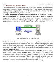
1- Input unit: - the input unit of a computer system accepts data,<br />
convert it into electrical impulses that are sent in to internal<br />
memory or to the central processing unit (CPU) where can be<br />
processed. Such as Punched cards(old system), Magnetic tap,<br />
Floppy disk, keyboard, mouse.
2012\2011<br />
سﺎﺑﺪﻟاﺮﻀﺧ ﻲﻠﻋ ﺪﺒﻋ ءﺎﺴﻴﻣ<br />
2-Central processing unit (CPU): -<br />
59<br />
بﻮﺳﺎﺤﻟا مﻮﻠﻋ ﻢﺴﻗ/<br />
ﺔﻴﺟﻮﻟﻮﻨﻜﺘﻟا ﺔﻌﻣﺎﺠﻟا<br />
The brain of any computer system is the CPU, which is<br />
sometime called “Processor” or “ Microprocessor” in personal<br />
computer.<br />
The CPU supervises and controls all of the peripheral equipment,<br />
perform arithmetic and makes logical decisions. The CPU is<br />
responsible for includes the data movement computations and<br />
logical operation necessary to convert data into meaningful<br />
information. It is divided into three sections: -<br />
2-1// Arithmetic and <strong>Logic</strong> unit (ALU).<br />
2-2// Control unit.<br />
2-3// Register.<br />
2-1 Arithmetic and <strong>Logic</strong> unit (ALU): -<br />
Perform the processing of data including arithmetic operations<br />
such as addition, subtraction, multiplication, division and logic<br />
operations including comparison (ex. A
2012\2011<br />
These operations include: -<br />
سﺎﺑﺪﻟاﺮﻀﺧ ﻲﻠﻋ ﺪﺒﻋ ءﺎﺴﻴﻣ<br />
1- Control to the input and output devices.<br />
2- entry and retrieval of information from memory.<br />
60<br />
بﻮﺳﺎﺤﻟا مﻮﻠﻋ ﻢﺴﻗ/<br />
ﺔﻴﺟﻮﻟﻮﻨﻜﺘﻟا ﺔﻌﻣﺎﺠﻟا<br />
3- routing of information between the memory and the arithmetic<br />
and logic unit.<br />
Control unit automatically coordinates the operation of the entire<br />
computer system, Although the control unit does not performed<br />
any actual processing on the data, It acts as a central nervous<br />
system uses to sent control signal to other units.<br />
2-3 Register: -<br />
Register are devices capable of sotring information, receiving<br />
data from other areas within the computer and transferring<br />
information as directed by the control unit, it is used for<br />
temporary storage of data or instruction and the most important<br />
register are: -<br />
1- program counter (PC): It contains the address of the next<br />
instruction to be executed.<br />
2- Instruction Register (IR): It contains the instruction being<br />
executed.<br />
3- Address Register (AR): holds the address of memory location.
2012\2011<br />
3- Output unit: -<br />
سﺎﺑﺪﻟاﺮﻀﺧ ﻲﻠﻋ ﺪﺒﻋ ءﺎﺴﻴﻣ<br />
61<br />
بﻮﺳﺎﺤﻟا مﻮﻠﻋ ﻢﺴﻗ/<br />
ﺔﻴﺟﻮﻟﻮﻨﻜﺘﻟا ﺔﻌﻣﺎﺠﻟا<br />
Output units are instruments of interpretation and<br />
communication between human and computer, that let you see<br />
(or here) the result of the commands you enter, the most common<br />
output device are a display screen (monitor), printer or other<br />
device that let you see what he computer has accomplished.<br />
The CPU execute each Instruction in a series of steps: -<br />
1- Fetch the next instruction from memory to IR.<br />
2- changes the program counter to point to the following<br />
instruction.<br />
3- Determine the type of the instruction to be fetched.<br />
4- IF the instruction uses data in memory determines where they<br />
are.<br />
5- Fetch the data into the internal CPU register.<br />
6- Execute the instruction.<br />
7- Store the result in the proper place.<br />
8- Go to step 1 to being executing the following instruction.<br />
4- Main Memory units: -<br />
The memory is the part of the computer that holds information<br />
(data and Instruction) for processing, main memory also known<br />
as primary or internal memory or primary storage, There are two<br />
types of main memory are ROM (Read Only Memory) and RAM<br />
(Random Access Memory).
2012\2011<br />
سﺎﺑﺪﻟاﺮﻀﺧ ﻲﻠﻋ ﺪﺒﻋ ءﺎﺴﻴﻣ<br />
62<br />
بﻮﺳﺎﺤﻟا مﻮﻠﻋ ﻢﺴﻗ/<br />
ﺔﻴﺟﻮﻟﻮﻨﻜﺘﻟا ﺔﻌﻣﺎﺠﻟا<br />
The specific function of main memory are to hold (store):<br />
1- All data to be processed.<br />
2- Intermediate result of processing.<br />
3- Final result of processing.<br />
A computer system generally includes two types of storage: -<br />
1- Primary storage<br />
2- Secondary storage
2012\2011<br />
1- Primary storage:-<br />
سﺎﺑﺪﻟاﺮﻀﺧ ﻲﻠﻋ ﺪﺒﻋ ءﺎﺴﻴﻣ<br />
There are two Primary storage Media: -<br />
1-1 Magnetic core storage<br />
63<br />
بﻮﺳﺎﺤﻟا مﻮﻠﻋ ﻢﺴﻗ/<br />
ﺔﻴﺟﻮﻟﻮﻨﻜﺘﻟا ﺔﻌﻣﺎﺠﻟا<br />
The second and third generation computers contained primary<br />
storage units composed of magnetic cores each core could store<br />
one bit when electricity flowed through the wire making up the<br />
cores a magnetic field was created the direction of the magnetic<br />
field was created the direction of the magnetic field determined<br />
which binary state s core represent a magnetic field in one<br />
direction indicate an one “1” condition a magnetic field in the<br />
other direction indicate an off “0” condition,<br />
So the core Memory stores data magnetically unlike<br />
semiconductor memory and operates at lower speed.<br />
1-2 Semiconductors memory<br />
It is a set of electronic circuits that put on the silicon chip. These<br />
circuit are often called “gates’ because they represent a (1) when<br />
current is permitted to flow and a (0) when it is not.<br />
The type of main memory contains a large number of<br />
semiconductor storage cells, each capable of storing one bit of<br />
information a bit which is a short of binary digit which either 1 or<br />
0 (full or empty).
2012\2011<br />
سﺎﺑﺪﻟاﺮﻀﺧ ﻲﻠﻋ ﺪﺒﻋ ءﺎﺴﻴﻣ<br />
4-1 Type of main memory: -<br />
There is basically two type of memory<br />
4-1-1 Random access memory (RAM):<br />
64<br />
بﻮﺳﺎﺤﻟا مﻮﻠﻋ ﻢﺴﻗ/<br />
ﺔﻴﺟﻮﻟﻮﻨﻜﺘﻟا ﺔﻌﻣﺎﺠﻟا<br />
And also called read/write memory, it is used for storing<br />
data and instruction, in this type the stored information will be<br />
lost when computers power is turned off so that it is called the<br />
volatile memory, its used only for temporary storage and the ram<br />
can be either dynamic or static.<br />
a- Static RAM: it is a semiconductor memory device in which<br />
the stored data will remain permanent<br />
stored as long as power is supplied without<br />
the need for periodically rewriting the data<br />
in to memory.<br />
b- Dynamic RAM: it is a semiconductor memory device in<br />
which the stored data will not remain<br />
permanent stored even with power is<br />
applied unless the data are periodically<br />
rewritten in to memory, the later<br />
operation is called a refresh operation.
2012\2011<br />
سﺎﺑﺪﻟاﺮﻀﺧ ﻲﻠﻋ ﺪﺒﻋ ءﺎﺴﻴﻣ<br />
4-1-2 Read only memory (ROM):<br />
65<br />
بﻮﺳﺎﺤﻟا مﻮﻠﻋ ﻢﺴﻗ/<br />
ﺔﻴﺟﻮﻟﻮﻨﻜﺘﻟا ﺔﻌﻣﺎﺠﻟا<br />
Is read only memory which can be read from but not written<br />
on so that it is called a non-volatile memory, when the user turn<br />
the computer off the content of ROM are not changed, the type of<br />
ROM is:<br />
1- Programmable Read Only Memory (PROM):<br />
It is prepared by the maker and can be electrical programmed<br />
by the user, it can not be erased and programmed a gain this<br />
means its content can never be changed.<br />
2- Erasable Programmable Read Only Memory (EPROM):<br />
The maker prepares it and can be electrical programmed by<br />
the user, it can be erase (deleted) by exposure to ultraviolet<br />
light and programmed many times.<br />
3-Electrically alterable Programmable Read Only Memory<br />
(EAPROM): read only memory that is electrically<br />
reprogrammable.
2012\2011<br />
سﺎﺑﺪﻟاﺮﻀﺧ ﻲﻠﻋ ﺪﺒﻋ ءﺎﺴﻴﻣ<br />
66<br />
بﻮﺳﺎﺤﻟا مﻮﻠﻋ ﻢﺴﻗ/<br />
ﺔﻴﺟﻮﻟﻮﻨﻜﺘﻟا ﺔﻌﻣﺎﺠﻟا
2012\2011<br />
سﺎﺑﺪﻟاﺮﻀﺧ ﻲﻠﻋ ﺪﺒﻋ ءﺎﺴﻴﻣ<br />
5-Secondary storage (External storage):-<br />
It can be classified into two type:<br />
67<br />
بﻮﺳﺎﺤﻟا مﻮﻠﻋ ﻢﺴﻗ/<br />
ﺔﻴﺟﻮﻟﻮﻨﻜﺘﻟا ﺔﻌﻣﺎﺠﻟا<br />
2-1 Mechanical storage devices: - is punched paper card and<br />
punched paper tape, both of this type is less popular now<br />
than the past.<br />
2-2 Magnetic storage devices: - In personal computer system ,<br />
external storage store information as magnetic spots on<br />
oxidizer surfaces because the magnetic spots do not need<br />
constant supply of power to refresh themselves, since 1 bit<br />
represented by magnetized spot and 0 is represented by the<br />
absence of magnetized spot.<br />
A magnetic devises can be classified into:<br />
2-2-1 sequential storage media.<br />
2-2-2 directs storage media.<br />
2-2-1 Sequential storage media as the magnetic tap in old<br />
computer system.<br />
2-2-2 directs storage media as the magnetic hard disk, magnetic<br />
floppy disk, and flash memories.<br />
1- Magnetic Hard Dick: A magnetic hard disk is a circular<br />
plate constructed of metal or plastic coated with magnetic<br />
material. Often both sides of the disk are used and<br />
several disks may be stacked on one spindle with<br />
read\write heads available on each surface. All disks<br />
rotate to together at high speed and are not stopped or<br />
started for access purpose. Bits are stored in the<br />
magnetized in sports along concentric circles called
2012\2011<br />
سﺎﺑﺪﻟاﺮﻀﺧ ﻲﻠﻋ ﺪﺒﻋ ءﺎﺴﻴﻣ<br />
68<br />
بﻮﺳﺎﺤﻟا مﻮﻠﻋ ﻢﺴﻗ/<br />
ﺔﻴﺟﻮﻟﻮﻨﻜﺘﻟا ﺔﻌﻣﺎﺠﻟا<br />
tracks. The minimum quantity of information which can be<br />
transferred is a sector. A magnetic hard disk is organized or<br />
formatting into tracks and sectors. Each track is divided<br />
into a number of sectors, and each track and sector has<br />
physical address that is used by the operating system to<br />
locate particular data record. Hard disks typically have<br />
from a few hundred to thousands of tracks. There are a<br />
constant number of tracks/sectors, with outer sectors using<br />
more surface area than the inner sectors. The arrangement<br />
of tracks and sectors on a disk is known as the format,<br />
shown in down hard disk scheme.<br />
Hard Disk<br />
Fig (3)
2012\2011<br />
سﺎﺑﺪﻟاﺮﻀﺧ ﻲﻠﻋ ﺪﺒﻋ ءﺎﺴﻴﻣ<br />
69<br />
بﻮﺳﺎﺤﻟا مﻮﻠﻋ ﻢﺴﻗ/<br />
ﺔﻴﺟﻮﻟﻮﻨﻜﺘﻟا ﺔﻌﻣﺎﺠﻟا<br />
* Hard Disk Performance: Several basic parameters<br />
determine the performance of a given hard disk drive.<br />
A seek operation is the movement of the read/write<br />
head to the desired track.<br />
1- Seek Time: A seek time is the movement of the<br />
read\write head to the desired track. The seek time is<br />
the average time for this operation to be performed.<br />
Typically, hard disk drives have an average seek time<br />
of several milliseconds, depending on the particular<br />
drive.<br />
2- Latency Time: The latency period is the time takes for<br />
the desired sector to spin under the head once the head<br />
is positioned over the desired track. Latency time<br />
depend on the constant rotational speed of the disk.<br />
• The sums of average seek time and the average latency<br />
time is the access time for the disk drive.<br />
2- Magnetic Floppy disk: The floppy disk is an older<br />
technology and derives its name because it is made of a<br />
flexible polyester material with a magnetic coating on both<br />
sides. The early floppy disks were 5.25 inch in diameter and<br />
were packaged in semiflexible jacket. Current floppy disks<br />
or diskettes are 3.5 inches in diameter and are encased in a<br />
rigid plastic jacket. A magnetic floppy disks transport<br />
consists of the electrical, mechanical, and electric<br />
components to provide the parts and control mechanism for<br />
a magnetic floppy disks unit.
2012\2011<br />
سﺎﺑﺪﻟاﺮﻀﺧ ﻲﻠﻋ ﺪﺒﻋ ءﺎﺴﻴﻣ<br />
70<br />
بﻮﺳﺎﺤﻟا مﻮﻠﻋ ﻢﺴﻗ/<br />
ﺔﻴﺟﻮﻟﻮﻨﻜﺘﻟا ﺔﻌﻣﺎﺠﻟا<br />
The floppy disks it self is a strip of plastic coated with a<br />
magnetic recording medium. Bits are recorded as magnetic spots<br />
on the floppy disk along several tracks. Read\write heads are<br />
mounted one in each track so that data can be recorded and read<br />
as a sequence of characters. Magnetic floppy disks units can be<br />
stopped, started to move forward or in reverse, or can be<br />
rewound.<br />
3- Flash Memories: Flash memories are high-density read\write<br />
memories (high-density translates into large bit storage<br />
capacity ) that are nonvolatile, which means that data can be<br />
stored indefinitely with out power they are sometimes used in<br />
place of floppy or small. Capacity hard disk drives in portable<br />
computers.<br />
High-density means that along number of cells can be packed<br />
into a given surface area on a chip, the higher density, the more<br />
bits that can be stored on a given size chip. This high density is<br />
achieved in flash memories with a storage cell that consists of<br />
single floating. A data bit is stored as charge or the absence of<br />
charge on the floating gate depending if a 0 or a 1 is stored.
2012\2011<br />
سﺎﺑﺪﻟاﺮﻀﺧ ﻲﻠﻋ ﺪﺒﻋ ءﺎﺴﻴﻣ<br />
Fig (4)Portions of hard disk drives<br />
Fig (5)Portions of hard disk<br />
71<br />
بﻮﺳﺎﺤﻟا مﻮﻠﻋ ﻢﺴﻗ/<br />
ﺔﻴﺟﻮﻟﻮﻨﻜﺘﻟا ﺔﻌﻣﺎﺠﻟا
2012\2011<br />
سﺎﺑﺪﻟاﺮﻀﺧ ﻲﻠﻋ ﺪﺒﻋ ءﺎﺴﻴﻣ<br />
Fig (6)Hard disk<br />
Fig (7)Floppy disk<br />
72<br />
بﻮﺳﺎﺤﻟا مﻮﻠﻋ ﻢﺴﻗ/<br />
ﺔﻴﺟﻮﻟﻮﻨﻜﺘﻟا ﺔﻌﻣﺎﺠﻟا
2012\2011<br />
1- Operating System:<br />
سﺎﺑﺪﻟاﺮﻀﺧ ﻲﻠﻋ ﺪﺒﻋ ءﺎﺴﻴﻣ<br />
Definition<br />
73<br />
بﻮﺳﺎﺤﻟا مﻮﻠﻋ ﻢﺴﻗ/<br />
ﺔﻴﺟﻮﻟﻮﻨﻜﺘﻟا ﺔﻌﻣﺎﺠﻟا<br />
An operating system is a program that acts as an<br />
intermediary between a user of a computer and the<br />
computer hardware. The purpose of an operating system is<br />
to provide an environment in which a user can execute<br />
programs. The primary goal of an operating system is thus<br />
to make the computer system convenient to use. A secondary<br />
goal is to use the computer hardware in an efficient manner.<br />
An operating system is an important part of almost every<br />
computer system. A computer system can be divided<br />
roughly into four components: the hardware, the operating<br />
system, the applications programs, and the users.<br />
2- Networking:<br />
A network is a set of devices (often referred to as nodes)<br />
connected by media links. A node can be a computer, printer,<br />
or any other device capable of sending and /or receiving data<br />
generated by other nodes on the network. The links connecting<br />
the devices are often called communication channels.<br />
Type of the network:<br />
1- LAN (Local Area Network).<br />
2- MAN(Metropolitan Area Network).<br />
3- WAN(Wide Area Network).
2012\2011<br />
3- Internet:<br />
سﺎﺑﺪﻟاﺮﻀﺧ ﻲﻠﻋ ﺪﺒﻋ ءﺎﺴﻴﻣ<br />
74<br />
بﻮﺳﺎﺤﻟا مﻮﻠﻋ ﻢﺴﻗ/<br />
ﺔﻴﺟﻮﻟﻮﻨﻜﺘﻟا ﺔﻌﻣﺎﺠﻟا<br />
Internet is the word-wide super network of computer<br />
networks that links computers around the word.<br />
URL: Each day when we use the Internet to check our mail<br />
online, visit a web page or browse an FTP folder, we use our<br />
browser. And while there can be a great number of Internet<br />
browsers out there, each of them offering different functions<br />
and boasting a different design, one thing that unites all of<br />
them is the fact that they are built with a single purpose - to<br />
handle URLs.<br />
* The URL<br />
Each file available on the World Wide Web can be identified<br />
and accessed through its corresponding URL. Standing for<br />
Uniform Resource Locator, a URL represents the global web<br />
address of documents, including web pages or image files, and<br />
programs such as CGI applications or Java applets. Its main<br />
mission is to identify the location of a document or a program<br />
available on the web and specify the mechanism for accessing it<br />
through a web browser.
2012\2011<br />
سﺎﺑﺪﻟاﺮﻀﺧ ﻲﻠﻋ ﺪﺒﻋ ءﺎﺴﻴﻣ<br />
4-Computer Classification:<br />
1) Computer Classification By: Betsy B.<br />
2) Personal Computer.<br />
3) Workstation.<br />
4) Video Game Console.<br />
5) Server.<br />
6) Client.<br />
7) Mainframe computer.<br />
8) Supercomputer.<br />
9) Handheld computer.<br />
10) Smart phone.<br />
11) Portable Media Player.<br />
12) Microcontroller.<br />
75<br />
بﻮﺳﺎﺤﻟا مﻮﻠﻋ ﻢﺴﻗ/<br />
ﺔﻴﺟﻮﻟﻮﻨﻜﺘﻟا ﺔﻌﻣﺎﺠﻟا
2012\2011<br />
سﺎﺑﺪﻟاﺮﻀﺧ ﻲﻠﻋ ﺪﺒﻋ ءﺎﺴﻴﻣ<br />
76<br />
بﻮﺳﺎﺤﻟا مﻮﻠﻋ ﻢﺴﻗ/<br />
ﺔﻴﺟﻮﻟﻮﻨﻜﺘﻟا ﺔﻌﻣﺎﺠﻟا<br />
5- Integrated Circuit Technologies: They are two types.<br />
1- VLSI: Very large-Scale Integration describe integrated<br />
circuits with complexities of form more than 10,000<br />
to 100,000 equivalent gates per chip.<br />
Figure (8) VLSI Circuit<br />
2-MSI: Medium-Scale Integration describe integrated circuits<br />
that have from 10 to 100 equivalent gates a chip. They<br />
include logic functions such as encoders, decoders,<br />
counters, registers, multiplexers, arithmetic, circuits,<br />
small memories, and others.<br />
Figure (9) MSI Circuit
2012\2011<br />
سﺎﺑﺪﻟاﺮﻀﺧ ﻲﻠﻋ ﺪﺒﻋ ءﺎﺴﻴﻣ<br />
77<br />
بﻮﺳﺎﺤﻟا مﻮﻠﻋ ﻢﺴﻗ/<br />
ﺔﻴﺟﻮﻟﻮﻨﻜﺘﻟا ﺔﻌﻣﺎﺠﻟا<br />
6-Translators program: system programming is a set of tools.<br />
1- Mechanical H/W & electronic circuits.<br />
2- S/W (system programming)<br />
• system programming have two purpose:<br />
1- They make a computer easy to use for none expert.<br />
2- They make it possible for the resource of the system to<br />
be used efficiently.<br />
• Software:<br />
1- Input /output subroutine. ﺔﺒﺳﺎﺤﻟا ﻦﻋ ﺪﻴﻌﺑ<br />
2- Monitor.<br />
3- Operating system. ﻞﻴﻐﺸﺘﻟا مﺎﻈﻧ<br />
4- Assemblers. ﻊﻴﻤﺠﺘﻟا ﺔﻐﻟ<br />
5- Microprocessors.<br />
6- Interpreters. ﺔﻐﻟ ﻞﻬﺳا<br />
7- Compiler. تﺎﻤﺟﺮﺘﻣ<br />
8- Linker, Loader. ﺔﻴﺴﻴﺋﺮﻟا ﺞﻣاﺮﺒﻟﺎﺑ ﺾﻌﺑ ﻊﻣ ﺞﻣاﺮﺒﻟا ﻂﺑﺮﻳ<br />
9- Editors. ﺔﺷﺎﺸﻟا ﻰﻠﻋ ﺞﻣاﺮﺑ لﺎﺧدا<br />
10- Debuggers. ﺞﻣﺎﻧﺮﺒﻟا ءﺎﻄﺧا ﺢﻴﺿﻮﺗ<br />
11- Database. تﺎﻧﺎﻴﺒﻟا راﺮﻜﺗ ﻰﻠﻋ ةﺮﻄﻴﺴﻟا<br />
12- Communication S/W. لﺎﺼﺗﻻا ﺔﻴﻠﻤﻌﺑ صﺎﺧ<br />
ﻞﻴﻐﺸﺘﻟا لاود م ﺪﺨﺘﺴﻳو
2012\2011<br />
سﺎﺑﺪﻟاﺮﻀﺧ ﻲﻠﻋ ﺪﺒﻋ ءﺎﺴﻴﻣ<br />
7-language Classification: they are three types:<br />
1- Procedure (using in Pascal language).<br />
2- Functional (using in Prolog language).<br />
78<br />
بﻮﺳﺎﺤﻟا مﻮﻠﻋ ﻢﺴﻗ/<br />
ﺔﻴﺟﻮﻟﻮﻨﻜﺘﻟا ﺔﻌﻣﺎﺠﻟا<br />
3- Object oriented C ++ (using in C ++ and visual C ++ language).<br />
8- Computer architecture: The internal architecture of the<br />
8086 family of microprocessor has changed a lot as part of<br />
the evolutionary process from the original 8086 to the 80386.<br />
They are implemented with simultaneously operating multiple<br />
processing units. Each unit has a dedicated function and they<br />
operate at the same time.<br />
The 8086 microprocessor contains just two processing units:<br />
The bus interface unit and execution unit.<br />
The 80286 microprocessor contains just four processing unit:<br />
1- Bus unit, 2- Instruction unit, 3- Execution unit,4- Address<br />
unit.<br />
The 80386 microprocessor contains just six functional units:<br />
1- Execution unit , 2- Segment unit, 3- Page unit, 4- Bus unit,<br />
5-Prefetch unit, 6- Decode unit.
2012\2011<br />
9- Computer generation:<br />
سﺎﺑﺪﻟاﺮﻀﺧ ﻲﻠﻋ ﺪﺒﻋ ءﺎﺴﻴﻣ<br />
79<br />
بﻮﺳﺎﺤﻟا مﻮﻠﻋ ﻢﺴﻗ/<br />
ﺔﻴﺟﻮﻟﻮﻨﻜﺘﻟا ﺔﻌﻣﺎﺠﻟا<br />
1- The first generation from 1946 to 1958 used electronic valves<br />
and frequent breakdowns and a rise in temperature due to the<br />
large size and weight. Use complex programming language.<br />
2-The second generation from 1958 to 1964 used transistors<br />
instead valves, small size, low coast, and high speed. Use high<br />
programming language.<br />
3- The third generation from 1965 to 1970 used complete<br />
circuit electronic, high speed, accuracy operations, and uses<br />
more users. Use high programming language.<br />
4- The fourth generation from 1971 to 1980 used complete<br />
circuit electronic involves large number of transistors, small<br />
size, high speed in save data and information.<br />
5- The fifth generation from 1980 to 1997 use complete circuit<br />
electronic very large and very high speed. As personal<br />
computer (PC), supper computer, and use artificial intelligent.
2012\2011<br />
سﺎﺑﺪﻟاﺮﻀﺧ ﻲﻠﻋ ﺪﺒﻋ ءﺎﺴﻴﻣ<br />
Circuit<br />
VLSI<br />
80<br />
بﻮﺳﺎﺤﻟا مﻮﻠﻋ ﻢﺴﻗ/<br />
ﺔﻴﺟﻮﻟﻮﻨﻜﺘﻟا ﺔﻌﻣﺎﺠﻟا
2012\2011<br />
سﺎﺑﺪﻟاﺮﻀﺧ ﻲﻠﻋ ﺪﺒﻋ ءﺎﺴﻴﻣ<br />
Circuit<br />
MSI<br />
81<br />
بﻮﺳﺎﺤﻟا مﻮﻠﻋ ﻢﺴﻗ/<br />
ﺔﻴﺟﻮﻟﻮﻨﻜﺘﻟا ﺔﻌﻣﺎﺠﻟا